

Page 1

SERVICE MANUAL
MULTIPLE OUTPUT LINEAR SYSTEM
DC POWER SUPPLY
AGILENT MODELS 6625A, 6626A,
6628A, and 6629A
Agilent Part No 06626-90003
Agilent Model 6625A, Serial 3738A-01389 through 01408
US37380101 and up
Agilent Model 6626A, Serial 3737A-02259 through 02328
US37370101 and up
Agilent Model 6628A, Serial 3738A-00683 through 00727
US37380101 and up
Agilent Model 6629A, Serial 3738A-00968 through 00997
US37380101 and up
* For instruments with higher Serial Numbers, a change page may be included.
5
Microfiche Part No. 06626-90004 Printed in Malaysia: September, 2001
Page 2

CERTIFICATION
Agilent Technologies certifies that this product met its published specifications at time of shipment from the factory. Agilent
Technologies further certifies that its calibration measurements are traceable to the United States National Bureau of
Standards, to the extent allowed by the Bureau’s calibration facility, and to the calibration facilities of other International
Standards Organization members.
WARRANTY
This Agilent Technologies hardware product is warranted against defects in material and workmanship for a period of three
years from date of delivery. Agilent software and firmware products, which are designated by Agilent for use with a
hardware product and when properly installed on that hardware product, are warranted not to fail to execute their
programming instructions due to defects in material and workmanship for a period of 90 days from date of delivery. During
the warranty period Agilent Technologies will, at its option, either repair or replace products which prove to be defective.
Agilent does not warrant that the operation of the software, firmware, or hardware shall be uninterrupted or error free.
For warranty service, with the exception of warranty optio ns, this product must be returned to a service facility designated
by Agilent. Customer shall prepay shipping charges by (and shall pay all duty and taxes) for products returned to Agilent
for warranty service. Except for products returned to Customer from another country, Agilent shall pay for return of
products to Customer.
Warranty services outside the country of initial purchase are included in Agilent’s prod uct pr ice, only if Customer pays
Agilent international prices (defined as destination local currency price, or U.S. or Geneva Export price).
If Agilent is unable, within a reasonable time to repair or replace any product to condition as warranted, the Customer shall
be entitled to a refund of the purchase price upon retur n of t he pr oduct to Agilent.
LIMITATION OF WARRANTY
The foregoing warranty shall not apply to defects resulting from improper or inadequate maintenance by the Customer,
Customer-supplied software or interfacing, unauthorized modification or misuse, operation outside of the environmental
specifications for the product, or improper site preparation and maintenance. NO OTHER WARRANTY IS EXPRESSED
OR IMPLIED. Agilent SPECIFICALLY DISCLAIMS THE IMPLIED WARRANTIES OF MERCH ANTABILITY AND
FITNESS FOR A PARTICULAR PURPOSE.
EXCLUSIVE REMEDIES
THE REMEDIES PROVIDED HEREIN ARE THE CUSTOMER’S SOLE AND EXCLUSIVE REMEDIES. Agilent
SHALL NOT BE LIABLE FOR ANY DIRECT, INDIRECT, SPECIAL, INCIDENTAL, OR CONSEQUENTIAL
DAMAGES, WHETHER BASED ON CONTRACT, TORT, OR ANY OTHER LEGAL THEORY.
ASSISTANCE
The above statements apply only to the standard product warranty. Warranty options, extended support contracts, product
maintenance agreements and customer assistance agreements are also available. Contact your nearest Agilent
Technologies Sales and Service office for further information on Agilent’s full line of Support Programs.
Page 3

SAFETY SUMMARY
The following general safety precautions must be observed during all phases of operation, service, and repair of this
instrument. Failure to comply with these precautions or with specific warnings elsewhere in this manual violates safety
standards of design, manufacture, and intended use of the instrument. Agilent Technologies assumes no liability for the
customer’s failure to comply with these requirements.
BEFORE APPLYING POWER.
Verify that the product is set to match the available line voltage and the correct fuse is installed.
GROUND THE INSTRUMENT.
This product is a Safety Class 1 inst rument (provided with a protective earth terminal). To minimize shock hazard, the instrument chassis
and cabinet must be connected to an electrical ground. The instrument must be connected to the ac power supply mains through a threeconductor power cable, with the third wire firmly connected to an electrical ground (safety ground) at the power outlet. For instruments
designed to be hard-wired to th e ac power lines (supply mains), conn ect the protective earth terminal to a protective conductor before any
other connection is made. Any interruption of the protective (grounding) conductor or disconnection of the protective earth terminal will
cause a potential shock h azard that could result in personal inju ry. If the instrument is to be energized via an external autotransformer for
voltage reduction, be certain that the autotransfo r mer common terminal is connected to the neutral (earthed pole) of the ac power lines
(supply mains).
FUSES.
Only fuses with the required rated current, voltage, and specified type (normal blow, time delay, etc.) should be used. Do not use repaired
fuses or short circuited fuseholders. To do so could cause a shock o r fire h azard.
DO NOT OPERATE IN AN EXPLOSIVE ATMOSPHERE.
Do not operate the instrument in the presence of flammable gases or fumes.
KEEP AWAY FROM LIVE CIRCUITS.
Operating personnel must not remove instrument covers. Component replacement and internal adjustments must be made by qualified
service personnel. Do not replace components with power cable connected. Under certain conditions, dangerous voltages may exist even
with the power cable removed. To avoid injuries, always disconnect power, discharge circuits and remove external voltage sources before
touching components.
DO NOT SERVICE OR ADJUST ALONE.
Do not attempt internal service or adjustment unless another person, capable of rendering first aid and resuscitation, is present.
DO NOT EXCEED INPUT RATINGS.
This instrument may be equipped with a line filter to reduce electromagnetic interference and must be connected to a properly grounded
receptacle to minimize electric shock hazard. Operation at line voltages or frequ encies in excess of those stated on the data plate may
cause leakage currents in excess of 5.0 mA peak.
SAFETY SYMBOLS.
Instruction manual symbol: the product will be marked with this symbol when it is necessary for the user to refer to the
instruction manual (refer to Table of Contents) .
Indicates hazardous vo ltages.
Indicate earth (ground) terminal.
The WARNING sign denotes a hazard. It calls attention to a procedure, practice, or the like, which, if not correctly
performed or adhered to, could result in personal inj ury. Do not proceed beyond a WARNING sign until the
indicated conditions are fully understood and met.
The CAUTION sign denotes a hazard. It calls attention to an operating procedure, or th e like, which, if not correctly
performed or adhered to, coul d result in damage to or destruction of part or all of the product. Do not proceed
beyond a CAUTION sign until the indicated conditions are fully understood and met.
DO NOT SUBSTITUTE PARTS OR MODIFY INSTRUMENT.
Because of the danger of introducing additional hazards, do not install substitute parts or perform any unau thorized modification to the
instrument. Return the instrument to an Agilent Technologies Sales and Service Office for service and repair to ensure that safety features
are maintained.
Instruments which appear damaged or defective should be made inoperative and secured against unintended operation until they can be
repaired by qualified service personnel
Page 4

SAFETY SUMMARY (continued)
GENERAL
Any LEDs used in this product are Class 1 LEDs as per IEC 825-1.
ENVIRONMENTAL CONDITIONS
This instrument is intended for indoor use in an installation category II, pollution degree 2 environment. It is designed to
operate at a maximum relative humidity of 95% and at altitudes of up to 2000 meters. Refer to the specifications tables for the
ac mains voltage requirements and ambient operating temperature range.
SAFETY SYMBOL DEFINITIONS
Symbol Description Symbol Description
Direct current Terminal for Line conductor on permanently
installed equipment
Alternating current Caution, risk of electric shock
Both direct and alternating current Caution, hot surface
Three-phase alternating current Caution (refer to accompanying documents)
Earth (ground) terminal In position of a bi-stable push control
Protective earth (ground) terminal Out position of a bi-stable push control
Frame or chassis terminal On (supply)
Terminal for Neutral conductor on
permanently installed equipment
Terminal is at earth potential
(Used for measurement and control
circuits designed to be operated with
one terminal at earth potential.)
Herstellerbescheinigung
Diese Information steht im Zusammenhang mit den Anforderungen der
Maschinenläminformationsverordnung vom 18 Januar 1991.
* Schalldruckpegel Lp <70 dB(A) * Am Arbeitsplatz * Normaler Betrieb
* Nach EN 27779 (Typprüfung).
Manufacturer’s Declaration
This statement is provided to comply with the requirements of the German Sound Emission Directive,
from 18 January 1991.
* Sound Pressure Lp <70 dB(A) * At Operator Position * Normal Operation
* According to EN 27779 (Type Test).
Off (supply)
Standby (supply)
Units with this symbol are not completely
disconnected from ac mains when t his switch is
off. To completely disconnect the unit from ac
mains, either disconnect the power cord or have
a qualified electrician install an external switch.
Edition 2 September, 2001
© Copyright 2001 Agilent Technologies, Inc.
Page 5

CONTENTS
Section I
INTRODUCTION
1-1 SCOPE ……………………………………………………1-1
1-2 SAFETY CONSIDERATIONS…………………………..1-1
1-3 INSTRUMENT AND MANUAL
IDENTIFICATION……………………………………….1-1
1-4 FIRMWARE REVISIONS ……………………………….1-1
Section II
PRINCIPLES OF OPERATION
2-1 INTRODUCTION ………………………………………..2-1
2-2 OVERALL BLOCK DIAGRAM DESCRIPTION
(Figure 2-1) ………………………………………………..2-1
2-3 AC Input Circuits ………………………………………..2-1
2-4 GPIB Board .……………………………………………... 2-1
2-5 Front Panel ……………………………………………….2-1
2-6 Output Boards …………………………………………2-1
2-7 GPIB BOARD (Figure 2-3) ……………………………... 2-3
2-8 GPIB Interface …………………………………………... 2-3
2-9 System MicroComputer…………………………………2-4
2-16 Output Boards Interface ………………………………...2-4
2-20 Front Panel Interface …………………………………...2-5
2-23 Bias Supply and Start Up ……………………………….2-5
2-24 OUTPUT BOARD ……………………………………… 2-7
2-25 Secondary Interface Circuits
(Figure 2-4) ……………………………………………… 2-7
2-37 Power mesh and Control Circuits
(Figure 2-5) …………………………………………… 2-10
Section III
VERIFICATION
3-1 INTRODUCTION ………………………………………..3-1
3-2 TEST EQUIPMENT REQUIRED ………………………3-1
3-3 OPERATION VERIFICATION TESTS ………………. 3-1
3-4 PERFORMANCE TESTS ………………………………..3-1
3-5 Introduction………………………………………………3-1
3-6 Measurement Techniques ………………………………3-1
3-10 Constant Voltage (CV) Tests ……………………………3-4
3-19 Constant Current (CC) Tests…………………………..3-10
3-27 EXTENDTED TESTS …………………………………...3-13
3-28 Output Drift Tests ……………………………………...3-13
Section IV
TROUBLESHOOTING
4-1 INTRODUCTION ………………………………………..4-1
4-2 ELECTROSTATIC PROTECTION ……………………..4-1
4-3 REMOVAL AND REPLACEMENT …………………...4-2
4-4 Top Cover Removal …………………………………….4-2
4-5 Gaining Access to Assemblies in the Supply …………4-2
4-6 GPIB Board Removal ..………………………………….4-2
4-8 DUSTCOVERS …………………………………………..4-4
4-9 Replacing the Power Module U338 ……………………4-4
4-10 Front Panel Removal …………………………………….4-4
4-11 Chassis Mounted Components ………………………...4-5
4-12 TEST EQUIPMENT REQUIRED ……………………….4-5
4-13 FUSE REPLACEMENT………………………………….4-5
4-14 INITIAL TROUBLESHOOTING AND BOARD
ISOLATION PROCEDURES ..…………………………4-8
4-15 Power-On Self Test ………………………………………4-8
4-16 Connector P201 Jumper Positions ……………………...4-9
4-17 ERROR Codes and Messages…………………………...4-9
4-18 GPIB BOARD AND FRONT PANEL
TROUBLESHOOTING PROCEDURES ……………...4-13
4-19 Test Setup ……………………………………………….4-13
4-20 Post Repair Calibration………………………………...4-13
4-21 Setting the Model Number
(MODEL Command) …………………………………...4-13
4-22 Signature Analysis Testing …………………………4-14
4-23 Test Setup for S.A. ……………………………………...4-14
4-24 Firmware Revisions (ROM? Command)……………..4-14
4-25 OUTPUT BOARD TROUBLESHOOTING
PROCEDURES ………………………………………….4-30
4-26 Test Setup ……………………………………………….4-30
4-27 Post Repair Calibration ………………………………..4-30
4-28 Self Exercise Routine on the Output Board ………….4-30
4-29 Troubleshooting Analog Multiplexer U323 and
Readback Using VMUX? Command …………………4-49
4-30 Understanding and Troubleshooting the Signal
Processor (U327)………………………………………...4-50
4-33 Power Module Signals …………………………………4-54
4-34 Miscellaneous Trouble Symptoms and Remedies ….4-54
Section V
REPLACEABLE PARTS
5-1 INTRODUCTION ………………………………………..5-1
5-2 HOW TO ORDER PARTS ………………………………5-1
i
Page 6

CONTENTS (Cont. )
Section VI
CIRCUIT DIAGRAMS
6-1 INTRODUCTION ………………………………………..6-1
6-2 FUNCTIONAL SCHEMATIC DIAGRAMS …………..6-1
6-3 COMPONENT LOCATION ILLUSTRATIONS ……...6-1
Appendix A
LOGIC SYMBOLOGY
ii
Page 7

LIST OF FIGURES
Figure Page
2-1 Agilent 6625A, 6826A, 6628A and 6629A Multiple Output Power Supplies, Block Diagram ……………………………...2-2
2-2 Output Operating Ranges for Agilent Models 6625A, 6626A, 6628A and 6629A …………………………………………2-3
2-2 HP-IB Board, Block Diagram ……………………………………………………………………………………………………..2-6
2-4 Output Board, Secondary Interface Circuits, Block Diagram ………………………………………………………………….2-9
2-5 Output Board, Power Mesh and Control Circuits, Block …………………………………………………………………….2-12
2-6 Voltage and Current Control Circuits, Simplified Schematic ………………………………………………………………..2-13
2-7 Typical Output Range Characteristics ………………………………………………………………………………………….2-14
2-8 Typical Downprogramming Characteristics Below 2.0 V …………………………………………………………………….2-16
2-9 Overvoltage Protection Circuits, Block Diagram ……………………………………………………………………………...2-17
3-1 Operating Ranges Available in Models 6625A, 6626A, 6820A and 6629A …………………………………………………..3-3
3-2 Current Monitoring Resistor Setup ………………………………………………………………………………………………3-4
3-3 Basic Test Setup …………………………………………………………………………………………………………………….3-5
3-4 Transient Recovery Time Test Setup …………………………………………………………………………………………….3-6
3-5 Transient Response Waveform. …………………………………………………………………………………………………..3-7
3-6 Negative Current Limit (- CC) Readback Accuracy ……………………………………………………………………………3-9
3-7 Down Programming Speed Test Setup ………………………………………………………………………………………3-12
3-8 CV Down Programming Speed Test Waveform ………………………………………………………………………………3-13
3-9 CV Up Programming Speed Test Setup ………………………………………………………………………………………..3-13
3-10 CV Up Programming Test Waveform ………………………………………………………………………………………….3-14
3-11 Fixed OV Protection Test Setup …………………………………………………………………………………………………3-14
3-I2 OV External Trip Test Connection ……………………………………………………………………………………………3-14
4-1 Agilent 6625A, 6626A, 6628A and 6629A Multiple Output Supplies, Assembly Locations ……………………………….4-3
4-2 HP-IB, Board, Fuse and Test Point Locations …………………………………………………………………………………...4-6
4-3 Output Board 1 and 2 Fuse and Test Point Locations ………………………………………………………………………….4-7
4-4 Output Board 3 and 4 Fuse and Test Point Locations ………………………………………………………………………….4-9
4-5 Initial Troubleshooting and Board Isolation …………………………………………………………………………………..4-13
4-6 HP-IB Board and Front Panel Troubleshooting ……………………………………………………………………………….4-15
4-7 Signature Analysis Test Setup ………………………………………………………………………………………………….4-17
4-8 Output Board Troubleshooting …………………………………………………………………………………………………4-29
4-9 Output Board Waveform During Self Exercise Routine ……………………………………………………………………4-35
4-10 DAC/Amplifier Circuit Troubleshooting ……………………………………………………………………………………...4-36
4-11 Overvoltage Troubleshooting …………………………………………………………………………………………………4-37
4-12 Output Held Low Troubleshooting ……………………………………………………………………………………………..4-39
4-13 Output Held High Troubleshooting …………………………………………………………………………………………….4-42
4-14 OV Circuit Will Not Trip Troubleshooting ……………………………………………………………………………………..4-43
4-15 Signal Processor U327, Overvoltage Circuit, Simplified Schematic …………………………………………………………4-46
4-16 Signal processor U327, Power-On/Start-Up Circuit, Simplified Schematic ………………………………………………4-46
4-17 Signal processor U327, Status Monitor Circuit, Simplified Schematic ………………………………………………………4-52
4-18 Status Problems Troubleshooting ……………………………………………………………………………………………….4-53
6-1 Power Distribution Schematic ….…………………………………………………………………………………………………6-3
6-2 GPIB Board, Component Location ……………………………………………………………………………………………….6-5
6-2 GPIB Board, Schematic Diagram ...……………………………………………………………………………………………….6-6
6-3 Output 1 & 2 Board, Component Location ..…………………………………………………………………………………..…6-7
6-3 Output 1 & 2 Board, Schematic Diagram .....…………………………………………………………………………………..…6-8
6-4 Output 3 & 4 Board, Component Location ..……………………………………….…………………………………………..6-13
6-4 Output 3 & 4 Board, Schematic Diagram .………………………………………….…………………………………………..6-14
iii
Page 8

LIST OF TABLES
Table Page
3-1 Test Equipment Required for Verification ………………………………………………………………………………………… 3-2
3-2 Low Range Voltage and Current Values …………………………………………………………………………………………… 3-4
3-3 Performance Test Record for Agilent 6625A and 6628A ...………………………………………………………………………. 3-15
3-4 Performance Test Record for Agilent 6626A and 6629A ………………………………………………………………………… 3-16
4-1 Test Equipment Required for Troubleshooting …………………………………………………………………………………… 4-5
4-2 Fuses …………………………………………………………………………………………………………………………………….4-6
4-3 Tests Performed at Power-On ..……………………………………………………………………………………………………… 4-8
4-4 Power-On Self Test Error Message ………………………………………………………………………………………………….. 4-9
4-5 ERROR Codes and Messages.………………………………………………………………………………………………………. 4-10
4-6
GPIB Board S.A. Test No. 1 ………………………………………………………………………………………………………… 4-18
4-7 GPIB Board S.A. Test No. 2 ………………………………………………………………………………………………………… 4-19
4-8 GPIB Board S.A. Test No. 3 ………………………………………………………………………………………………………… 4-20
4-9 GPIB Board S.A. Test No. 4 ………………………………………………………………………………………………………… 4-21
4-10 GPIB Board S.A. Test No. 5 ………………………………………………………………………………………………………… 4-22
4-11 GPIB Board S.A. Test No. 6 ………………………………………………………………………………………………………… 4-23
4-12 GPIB Board S.A. Test No. 7 ………………………………………………………………………………………………………… 4-24
4-13 GPIB Board S.A. Test No. 8 ………………………………………………………………………………………………………… 4-25
4-14 Keyboard Signal Paths ………………………………………………………………………………………………………………. 4-27
4-15 Microcomputer (U312) Signal Measurements During the Self Exercise Routine …………………………………………… 4-44
4-16 U368 Signal Levels …………………………………………………………………………………………………………………… 4-45
4-17 Signal Processor (U327) Signal Levels …………………………………………………………………………………………….. 4-47
4-18 Typical Power Module Voltage Levels ……………………………………………………………………………………………. 4-49
4-19 Miscellaneous Trouble Symptoms …………………………………………………………………………………………………. 4-50
5-1 Output Board Configurations ……………………………………………………………………………………………………….. 5-1
5-2 Reference Designators ………………………………………………………………………………………………………………… 5-1
5-3 Abbreviations …………………………………………………………………………………………………………………………...5-2
5-4 Federal Manufacturer Codes ………………………………………………………………………………………………………… 5-3
5-5 Chassis Parts …………………………………………………………………………………………………………………………… 5-4
5-6 Output Board Replacement Part List …………………………………………………………………………………………………5-7
5-7 25W/.5A Replacement Parts List ……………………………………………………………………………………………………. 5-9
5-8 50W/2A Replacement Parts List …………………………………………………………………………………………………… 5-18
iv
Page 9

Section I
INTRODUCTION
1-1 SCOPE
This manual contains principles of operation, verification,
and troubleshooting information for the power supply.
Replaceable parts lists and circuit diagrams are also
provided. Installation, operation, programming, and
calibration procedures as well as detailed specifications are
given in a separate Operating Manual, Agilent Part No.
06626-90001.
Wherever applicable, the service instructions given in this
manual refer to pertinent information provided in the
Operating Manual. The information in each manual covers
model 6625A, 6626A, 6628A, and 6629A. The main
differences between the models are the number and type of
outputs each model contains. These differences are specified
in each of the manuals.
The following is a listing of the information contained in this
manual with a brief description concerning its scope and
purpose.
Principles of Operation: Section II provides block diagram
level descriptions of the supply’s circuits. The GPIB
interface (digital circuits), the power control (analog and
digital circuits), and power output (analog circuits) are
described. These descriptions are intended as an aid in
troubleshooting.
Verification: Section III contains test procedures that check
the operation of the supply to ensure that it meets the
specifications given in Section I of the Operating manual.
Troubleshooting: Section IV contains board level
troubleshooting procedures to isolate a malfunction to a
defective board (GPIB or output board) or assembly (front
panel, power transformer, or cable assembly). Additional
troubleshooting procedures are provided to isolate the fault
to a defective component on the board. Board and assembly
level removal and replacement procedures are also given in
this section.
NOTE
Calibration is generally required after a repair is made.
Software calibration procedures are given in Appendix A
of the Operating Manual. After calibration is completed,
perform the applicable test(s) given in Section III of this
manual to ensure that the supply meets all specifications.
Replaceable Parts:
replaceable parts for all electronic components and
mechanical assemblies.
Section V provides a listing of
Circuit Diagrams:
and component location diagrams . The names that appear
on the functional schematics also appear on the block
diagrams in Section II. Thus, the descriptions in Section II
can be correlated with both the block diagrams and the
schematics.
Section VI contains functional schematics
Logic Symbology:
the logic symbols used on the functional schematics.
Fault Indicator (FLT) and Remote Inhibit (INH): A fault
indicator and remote inhibit circuit, which provide
additional shutdown protection should either the GPIB
and/or controller fail, are available optionally. See a
separate document entitled, "Appendix E Option 750
Operating Instructions" for the Multiple Output Linear
System DC Power Supply Agilent Models 662xA (Agilent
P/N 5957-6372).
Appendix A gives a brief description of
1-2 SAFETY CONSIDERATIONS
This product is a Safety Class 1 instrument, which means
that it is provided with a protective earth terminal. The
instrument and this manual should be reviewed for safety
markings and instructions before operation. Refer to the
Safety Summary page at the beginning of this manual for a
summary of general safety information. Safety information
for specific procedures is located at appropriate places in the
manual.
1-3 INSTRUMENT AND MANUAL
IDENTIFICATION
Agilent Techonologies instruments are identified by a twopart Serial number, i.e. 2601A-00101. The first part of the
serial number (the prefix) is a number/letter combination
that denotes either the date of manufacture or the date of a
significant design change. It also indicates the country of
manufacture. The first two digits indicate the year (25 =
1985, 26 = 1986, etc), the second two digits indicate the week,
and “A” designates the U.S.A. The second part of the serial
number is a different sequential number assigned to each
instrument.
1-1
Page 10

If the serial number prefix on your power supply differs
from that shown on the title page of this manual, a yellow
Manual Change sheet that is supplied with the manual
add/or manual backdating changes in Appendix A of this
manual define the differences between your supply and the
supply described in this manual. The yellow change sheet
may also contain information for correcting errors in the
manual.
The serial number prefixes listed on the front of this manual
indicate the versions of the supplies that were available
when the manual was issued. If the serial prefix of your
supply is not listed in this manual, the manual may include
a yellow “Manual Changes” sheet. That sheet updates this
manual by defining any differences between the version of
your supply and the versions included here, and may also
include information for correcting any manual errors. Note
that because not all changes to the product require changes
to the manual, there may be no update information required
for your version of the supply.
1-4 FIRMWARE REVISIONS
The Read Only Memory (ROM) chip inside of your supply is
identified with a label that specifies the revision of the
supply’s firmware, see paragraph 4-24
1-2
Page 11

Section II
PRINCIPLES OF OPERATION
2-1 INTRODUCTION
The following paragraphs provide block diagram level
descriptions of the power supplies. Differences between the
models are given as required. The descriptions provide a
basic understanding of circuit operation and are intended as
an aid in troubleshooting . It is assumed in the following
discussions that you are familiar with the operating and
programming instructions presented in the Operating
Manual (Agilent Part No. 06626-90001).
2-2 OVERALL BLOCK DIAGRAM DESCRIPTION
(FIGURE 2-1)
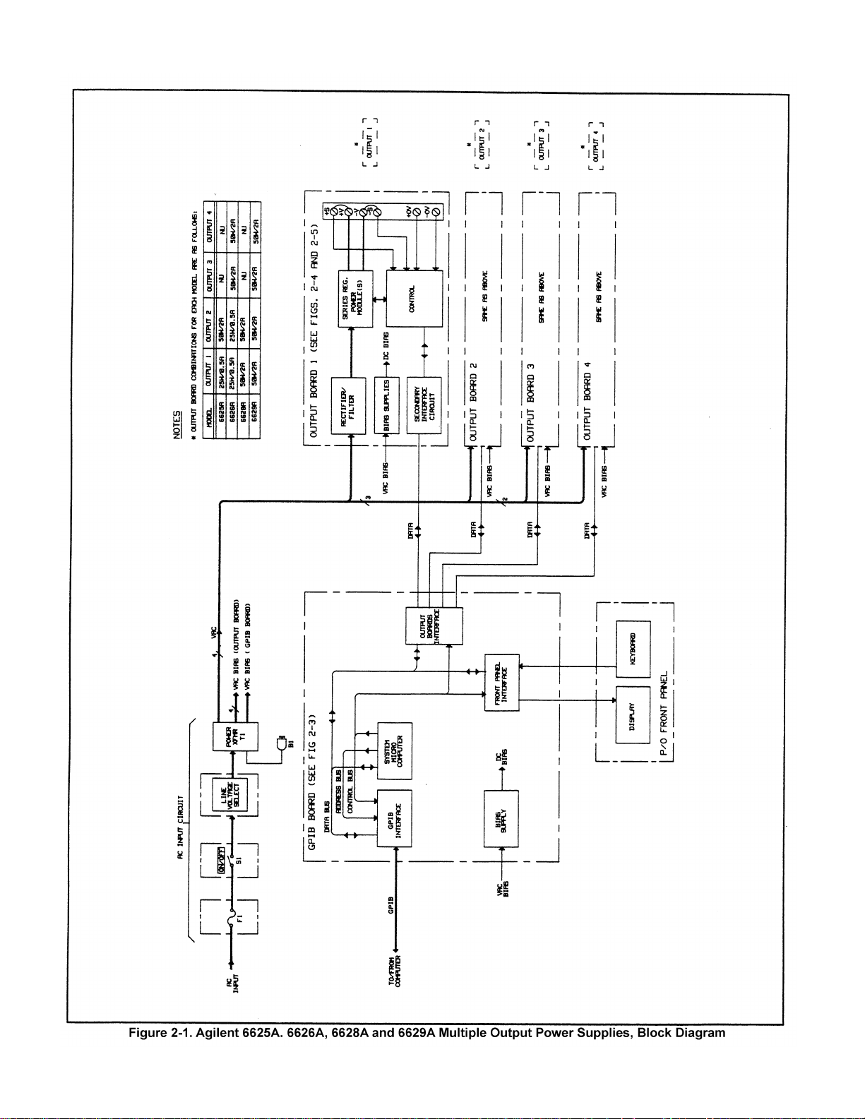
Figure 2-1 is a block diagram that illustrates the major
assemblies contained within the power supply. As shown in
the figure, each supply includes ac input circuits, an GPIB
board, front panel display and keyboard, and two or more
output boards.
2-3 AC Input Circuit
The ac input circuit consists of a line module on the rear
panel of supply, front panel ON/OFF switch S1, power
transformer (T1), located in the front of the chassis, and a
cooling fan located in the rear of the chassis. The line module
contains a voltage selector card that selects the applicable ac
input voltage: 100 Vac, 120 Vac, 220 Vac, or 240 Vac. The
voltage card selection must match the nominal line voltage
that is connected to the unit. The line module also contains
the main fuse F1. An 8 A fuse (normal blow) must be
installed for a 100/120 VAC input; a4 fuse (normal blow)
must be installed for a 220/240 VAC input. The ac input is
applied to the power transformer when S1 is ON.
Depending on the line module setting, the 120 Vac cooling
fan either runs directly from the line module setting, the 120
VAC cooling fan either runs directly from the line or from
the appropriate transformer tap. The power transformer
provides the main ac inputs to the output boards and also
provides the ac inputs for the bias voltage supplies located
on the GPIB board and each output board. Ac power
distribution is shown in detail in Figure 6-1 in the rear of this
manual.
2-4 GPIB Board
The GPIB board contains the GPIB interface, system
microcomputer, output boards interface, and front panel
interface. These circuits provide the interface between the
user and the multiple outputs of the power supply. Each
output board is actually an output channel that can be
individually selected and controlled over the GPIB or from
the supply’s front panel. The GPIB board inter prets
commands from the GPIB or from the front panel to
control the selected output. The GPIB board also processes
measurement and status data received from the output
boards. This data may be read back to the controller over
the GPIB and/or displayed on the supply’s front panel.
Also, each output board can be individually calibrated over
the GPIB using calibration commands (See Appendix A in
Operating Manual). Correction factors are calculated during
calibration and stored in non-volatile memory on the GPIB
board. The GPIB board is described in greater detail in
paragraph 2-7.
2-5 Front Panel
Most of the remote operations that can be performed via the
GPIB can also be performed from the supply’s front panel.
In addition to the ON/OFF switch already mentioned, the
front panel contains an LCD display and a keypad. The LCD
display consists of an alphanumeric display and status
annunciators. The LCD normally displays the measured
output voltage and current of the selected output. When
programming an output from the front panel keypad, the
selected output channel, the function being programmed,
and the present value will be displayed. The annunciators
indicate which output channel has been selected and give
GPIB and power supply status information. The keypad
allows control of the supply’s system functions as well as
individual control of each output channel. Detailed
instructions on using the front panel’s display and keypad
are given in the Operating Manual.
2-6 Output Boards
The Agilent 6625A and 6628A contain two output boards
and the Agilent 6626A and 6629A contain four output
boards. The output combinations that correspond to each
model are shown in Figure 2-1. Each isolated output can
supply power in two ranges as shown in Figure 2-2. This
flexibility allows you to use the same output to power loads
with different voltage and current requirements. The output
ranges and operating characteristics of each output are
described in greater detail in Section IV of the Operating
Manual.
As shown in Figure 2-1, each output board contains a
rectifier/filter, power module, control circuit, secondary
interface circuit, and bias supplies.
The ac input to each output board is rectified, filtered, and
applied to the power module regulator. Each output board
employs series regulation techniques. The regulator element
is connected in series with the load and operates in the linear
region (between saturation and cutoff) of the transistor
characteristic curve. Regulation is achieved by varying the
conduction of the series element in response to changes in
the line voltage or the load. The constant voltage CV control
circuit compares the voltage at the output with a reference
voltage and generates a control signal which varies the
conduction of the series regulator to raise or lower the
output voltage as required. The constant current CC control
2-1
Page 12
2-2
Page 13

Circuit compares the voltage at the current monitor resistor
with a reference and likewise varies the conduction of the
series regulator.
The interface circuit on the output board receives digital
signals from the GPIB board and converts them to analog
signals (reference voltages) which are sent to the control
circuit to program the output voltage and current.
The output boards can be commanded to send measurement
and status data back to the GPIB controller and/or to the
display on the front panel. The data is sent back via the
secondary interface circuit and the appropriate circuits on
the GPIB board.
The output board is able to sink current as well as source
current. Current sink limits are fixed at values slightly
higher than the maximum current source limit for the
particular output voltage operating point. See Figure 2-7 for
typical current source and sink characteristics. The output
board circuits are described in greater in paragraph 2-24.
2-7 GPIB BOARD (FIGURE 2-3)
Figure 2-3 illustrates the major circuits and signal flow on
the GPIB board. Complete circuit details are shown on the
functional schematic in the rear of this manual.
The functional names on the block diagram correspond with
those on the schematic so that the diagrams can be
correlated. As shown in Figure 2-3, the major circuits consist
of the GPIB interface, the system micro-computer, the
output boards interface, and the front panel interface circuit.
2-8 GPIB Interface
These circuits consist of the GPIB bus connector (J201),
transceivers (U203) for the 8 data lines and 8 control lines,
and the GPIB talker/listener chip (U202). All GPIB (IEEE-
488) functions are implemented by the GPIB chip which
handles data transfer between the microprocessor and the
GPIB, handshake protocol, and talker/listener addressing
procedures. The GPIB talker/listener chip is connected to
the data bus and appears as memory locations to the
microprocessor.
The eight data lines (DIO1-DIO8) of the GPIB are reserved
for the transfer of data and other messages in a byte serial,
bit parallel manner. Data and message transfer is
asynchronous, coordinated by the three handshake lines
(DAV, NRFD, and NDAC). The power supply can be a talker
or a listener on the GPIB. The controller dictates the role of
an GPIB device by setting the ATN (attention) line true and
sending talk or listen addresses on the data lines (DIO1DIO8). The power supply’s GPIB address is stored in the
EEPROM (electrically erasable programmable memory) chip
along with other system variables. You can find out your
supply’s GPIB address by using the front panel ADDR key
as described in the operating manual. As shipped from the
factory, the power supply’s address is set to 5. Any address
from 0 through 30 is a valid address.
There are five GPIB control lines: ATN, IFC, REN, SRQ, and
EOI (IEEE-488). When the controller sets the ATN line true,
all devices on the bus must “listen” to the addresses and
universal commands placed on the bus. When ATN is false,
only devices that are addressed will actively send or receive
data. All unaddressed devices will ignore the data lines
when ATN is false.
2-3
Page 14

2-9 System Micro-Computer
The system micro-computer decodes and executes all
instructions, and controls all data transfers. It consists of a
microprocessor, an address decoder, RAM and ROM
memories, data buffers/latches, and a real time clock as
shown in Figure 2-3.
2-10 Microprocessor and Clock Circuits. These circuits
contain a high performance 8-bit microprocessor(U201) and
associated clock circuits. The microprocessor operates on a 1
MHz cycle, which it derives from a 4 MHz ceramic resonator
oscillator(Y201). The 1 MHz Q signal is generated by the
microprocessor for use by other circuit.
A 4 millisecond (approximately) clock signal, applied to the
microprocessor interrupt input, enables the microprocessor
to keep track of real time. This allows the microprocessor to
form necessary tasks on a regular basis. The real time clock
signal is also used to keep track of the time that has elapsed
since the output was last changed. This enables
microprocessor to determine if a CV/CC mode change
occurred before the selected time delay (see Reprogramming
Delay discussion in Section V of the Operating Manual). The
microprocessor inhibits the OCP function until the delay is
over.
The microprocessor also uses the 4 millisecond clock to
determine when to refresh the front panel display and to
perform other regularly scheduled jobs.
The R/W (read/write) output from the microprocessor
indicates the direction of flow on the data bus, either to or
from the microprocessor. A low level R/W signal indicates
that the microprocessor is writing data onto the data bus. A
high level R/W signal indicates that the microprocessor is
reading data that was placed on the bus by the addressed
circuit. The microprocessor uses the address decoder circuit
and the address bus to specify the data transfer locations.
Addresses are valid on the rising edge of the Q signal.
2-11 Data Bus latches (U217) and Buffers (U216). The
timing sequence of the microprocessor is such that the
circuits providing data for the microprocessor are deselected (address disappears) before the microprocessor can
read the data. The data bus latches (U217) latch the data to
be read by the microprocessor. The data is updated on every
falling Q pulse. Data put on the data bus by the
microprocessor goes around the latches though buffers
(U216).
2-12 Free-Run and Signature Analysis Jumpers. The data
bus is connected to the microprocessor through a jumper
pack (W202). For some signature analysis tests of the
microprocessor kernel (microprocessor, RAM, ROM), the
data bus is broken by moving W202 from the NORMAL
position to the NOP position (see paragraph 4-23). This
connects a NOP (no operation) code (free run) to the
microprocessor data inputs. The NOP code does not contain
an address for the next instruction so the microprocessor
goes to the next highest address. Therefore, the address bus
looks like a 16-bit counter that continuously rolls over and
_
_
_
_
_
_
_
starts at zero. The contents of each address appear
sequentially on the data bus (other side of the break) In
addition, for all signature analysis tests, jumper W201
must be moved from the NORM RUN position to the SIG
ANALYSIS position (see paragraph 4-23).
2-13 Address Bus and Address Decoder. The
microprocessor has 16 address lines (A0-A15) allowing it to
address 65,536 locations. The address decoder (U208) allows
each addressable circuit to look at a shorter address. The
chip select signals (CS0-CS8) are decoded from the higher
order address lines (A12-A15). When a data buffer’s CS is
decoded, it places its data on the data bus lines. When a data
latch’s CS is decoded, the output of each latch will be set to
the logic state that is present on the associated data bus line.
If the chip select for the RAM (random access memory),
ROM (read only memory), or talker/listener chip is
decoded, the selected circuit will decode the lower order
address bits supplied to it on the address bus.
2-14 Memory (ROM and RAM). The system microcomputer
contains both ROM (U206) and RAM (U207) devices. The
32KK non-volatile ROM contains the operating program and
parameters. The 2 K static RAM stores variables voltage to
be programmed, output current readback, etc. A third
memory chip, shown in the output board interface block of
Figure 2-3, is the EEPROM (electrically erasable
programmable memory). The EEPROM (U230) stores all of
the system constants including calibration constants, the
supply’s GPIB address, and model number (see paragraph
2-19).
2-15 Real Time Clock. The real time clock (U209) consists
of a 14-stage ripple counter that divides the 1 MHz Q clock
signal from the microprocessor to produce a pulse every 4
milliseconds. The real-time clock is used by the
microprocessor to schedule regular jobs as described
previously. The TIMER ENABLE signal resets the counter to
zero.
___________
__
_
__
_
2-16 Output Boards Interface
This circuit provides the interface between the system
microcomputer and each of the output boards (up to 4) in
the power supply. Data is transferred serially one bit at a
time between latches/buffers on the GPIB board and
optoisolators on the output boards. As shown in Figure 2-3,
the latches/buffers use data bus lines D0-D3 to send/receive
data from the applicable output. Data line D0 is used for
output board 1, D1 for output board 2, D2 for output board
3 (if present), and D3 for output board 4 (if present). A
controlled and regulated 5 volt line is also generated on the
GPIB board to operate art of the opto-isolators on the
output boards. In addition to interfacing with the output
boards, the latches/buffers interface with the 4 K bit serial
EEPROM in which system constants are stored.
2-17 Data Buffers. These 3-state buffers (U212) place the
serial data from each output board and the EEPROM on the
supply’s system microcomputer data bus lines when chip
__
select CS3 is decoded. Serial data from output boards 1-4
appears on data bus lines D0-D3, respectively, and EEPROM
_
2-4
Page 15

serial output data appears on data bus line D7. Logic 0’s will
always appear on data bus lines D4-D6 when CS3 is
decoded because these buffer inputs are connected to
COMMON. All buffer output are held in the high
impedance state when CS3 is not decoded.
2-18 Data Latches. These stages (U213) are edge-triggered
D-type flip-flops. On the rising edge of the CS2 chip select,
the output of each stage will be set to the logic state that is
present on the associated data bus line. Data bus line D0-D3
are the serial data input lines for output boards 1-4,
respectively. Data bus line D4 controls the TIMER ENABLE
signal line to the real time clock circuit; D5 is the chip select
line for the EEPROM; D6 is the clock signal for the
EEPROM; and D7 is the data input line for the EEPROM.
The data that is transferred between the GPIB board and
the output boards (up to 4) passes through optical isolators
located on each output board.
2-19 EEPROM. This 4 K bit serial EEPROM (electrically
erasable programmable memory) stores the power supply’s
GPIB address and model number as well as the constants
used in calibrating the supply. The EEPROM (U230) is
nonvolatile allowing it to retain the stored information after
power is cycled off and on.
Because the RAM operates faster than the EEPROM, at
power on, the stored data is read into RAM in the system
microcomputer via data bus line D7.
The EEPROM’s 4096 bits of read/write memory are divided
into 2 pages of 8 X 256 each. Each register can be serially
read from or written to using data bus line D7. Input data is
received via a data latch and output data is sent via a data
buffer.
Data written to the EEPROM is stored in a location until it is
updated by a write cycle. The CHIP SELECT and CLOCK
signals are use by the microprocessor to control the
EEPROM’s programming modes. AT power on, the
EEPROM signal holds the EEPROM’s CLOCK signal off to
protect against accidental data writes when power is initially
applied.
__
_
__
___________
__
_
_
2-20 Front Panel Interface
These circuits provide the interface between the supply’s
system microcomputer and the front panes (keyboard and
LCD display). The microprocessor uses the data latches
(U210 ) and data buffers (U214) to transfer data between the
supply’s system microcomputer and the front panel.
2-21 Data Latches. On the rising edge of the CS5 chip select
these D-type flip-flops will be set to the logic states that are
present on the data bus lines.
Data bus lines D2-D7 are fed directly to the front panel
display to indicate power supply conditions The LCD
display may indicate the output voltage and current for a
selected output board, the present function being
programmed, a programmed message, or an error message.
__
_
The annunciators provide operating and status information.
The microprocessor uses the real time clock to determine
when update/refresh the display.
Data bus line D0-D2 are fed to the 3 to 8 line keyboard
decoder (U211). The microprocessor successively drives
each of the eight open collector outputs of the decoder and
monitors the four readback lines from the keyboard to
determine which key was pressed. The readback lines are
held high until a depressed key pulls the line low.
2-22 Data Buffers. These 3-state buffers place the keyboard
readback data on data bus lines D4-D7 when chip select CS4
is decoded. As stated above, the microprocessor will use this
information to determine which key was pressed. In
addition buffers provide the following data on bus lines D0D3 when CS4 is decoded:
or
a logic 0 (Jumper W201 is installed in the Skip
D1 - A logic 1 (Jumper W201 is not installed in the
or
a logic 0 (Jumper W201 is installed in the Cal
D2 - A logic 0 indicates Remote Inhibit is true
D3 - A logic 1 indicates OPTION 750 is installed in
All buffer outputs are held in the high impedance state
disconnecting it from the data bus when CS4
__
_
D0 - A logic 1 (Jumper W201 is not installed in the
Skip Self Test position) – tells the
microprocessor to perform the self test at
power on;
Self Test position) – tells the microprocessor
not to perform self test at power on.
Cal Lockout position) – tells the
microprocessor to respond to calibration
commands;
Lockout position ) – tells the microprocessor
to ignore calibration commands. This jumper
provides security against unauthorized
calibration.
(OPTION 750).
power supply.
__
_
is not decoded.
2-23 Bias Supply and Start-Up Circuit
The bias supply (U218) provides + 5 V bias power to operate
the circuits on the GPIB board. The start-up circuit (U220,
U222) generates the OPTO PON signal (delayed +5 V) which
is used to power the optical-isolators on the output boards.
The OPTO PON signal is initially held low for
approximately 100 ms to prevent the erroneous transfer of
data at power on. The start-up circuit also generates PCLR
(power clear) and EEPON (EEPROM power on) signals
when power is turned on. The PCLR signal is held low at
power on to initialize the talker/listener and microprocessor
chips. The EEPON signal is held low at power onto disable
the EEPROM clock. Thus, the start up circuit delays turning
on the microprocessor and optoisolators until the bias
voltages have stabilized. If the line voltage drops after the
unit has been turned on, the start-up circuit will again
generate the low level signals to disable the interface and
remove power from the supply’s outputs.
2-5
_____
_
__
_____
_
_
Page 16

2-6
Page 17

2-24 OUTPUT BOARD
The following paragraphs provide block diagram level
descriptions of the output board. The descriptions cover the
two output board types. Differences between the board
types are given as required. Figure 2-1 shows which output
board types are used in the power supplies.
The descriptions that follow are divided into two main block
diagram discussions: Secondary Interface Circuits and
Control Circuits. The block diagrams illustrate the major
circuits and signal flow on an output board. Complete
circuit details are shown on the output board functional
schematic Figure 6-3 in the rear of the manual. The
functional names on the block diagrams correspond with
those on the functional schematic.
2-25 Secondary Interface Circuits (Figure 2-4)
These circuits receive digital signals from the GPIB board
and convert them to analog signals (voltages) which are sent
to the power mesh and control circuits to program the
output voltage, output current, and overvoltage.
Measurement and status signals are sent back to the
secondary interface circuits from the power mesh and
control circuits to be processed before they are sent on to the
GPIB board and then to the GPIB controller and/or the
front panel. The following paragraphs describe the interface
circuits shown in Figure 2-4.
2-26 Microcomputer. This 8-bit microcomputer (U312)
contains a CPU, ROM, and RAM. These internal circuits
process all data that is transferred between the GPIB board
and the power mesh and control circuits on the output
board. GPIB board data is transferred serially via optical
isolators which connect incoming data to an input port on
the microcomputer and outgoing data to an output port on
the microcomputer.
On the output board side, the microcomputer uses an 8-bit
parallel bi-directional data bus to program DACs which
control the output voltage, output current, overvoltage
setting, and sets the readback DAC. Various status and
operating conditions are read back on the data bus. The
microcomputer also generates address and control signals
which are used by other interface circuits. The interrupt
input to the microcomputer is used in conjunction with
readback monitor switches (U365, U366, and U368) analog
multiplexer (U323) and DAC (U321) to perform a successive
approximation A/D conversion in order to readback output
voltage and current values as well as various test point
voltages.
2-27 Address Decoder. This circuit (U320) decodes
addresses sent by the microcomputer and generates the
appropriate chip select signal (CS0 – CS6) to select which
circuit sends or receives data. CS0 selects the status monitor
(part of U327) to send status data back to the microcomputer
on data bus lines D0-D5. CS1-CS4 determine which DAC
will receive data. CS1 selects the 14-bit CV (Constant
Voltage) DAC, CS2 selects the 14-bit CC (Constant Current)
DAC, CS3 selects the 14-bit Readback DAC and CS4 selects
__
_
__
_
__
_
__
_
__
_____
_
__
_
_
_
__
_
the 8-bit OV (Over Voltage) DAC. C55 selects the
programming latches (U367), and CS6 selects the readback
monitor switches (U365, U366, and U368). The digital inputs
(D0 – D7) to the DAC’s are derived from the GPIB
controller or from the front panel depending upon whether
the supply is in the remote or local mode.
2-28 CV DAC. The 14-bit CV DAC (U313) and amplifier
(U360) convert the digital input signal from D0 –D7
supplied through latches (U369) into an analog signal (CV
PROG) in the range of 0 to – 10 Volts. This output signal is
used as a reference voltage and is send to the voltage control
circuits (see paragraph 2-46) to set the output voltage to the
programmed value.
The most significant bits (MSB’s) are loaded into the input
register of U313 from the data bus when: address line A3
goes high, address line A4 goes low, and CS1 goes low. The
least significant bits (LSB’s) are loaded into the input register
of U313 from the data bus when: address line A3 goes low,
address line A4 goes high, and CS1 goes low. The data in the
input register in transferred to the DAC of U313 when:
address line A3 is high, address line A34 is high, and CS1 is
low.
CV PROG is also sent to the analog multiplexer so that it can
be measured during power on self test.
U369 and U370 provide isolation between the 8-bit data bus
and the CV/CC DAC’s. This isolation assures that signals on
the data bus will not be capacitively coupled through the CV
and CC DAC’s as noise.
2-29 CC DAC. The 14-bit CC DAC (U314) and amplifier
(U361) convert the digital input signals in a similar manner
as the CV DAC into a analog signal (CC PROG) in the range
of 0 to - 10 Volts. This signal is used as a reference voltage
and is sent to the current control circuits (see paragraph 2-
47) to set output current to the programmed value.
The most significant bits (MSB’s) are loaded into the input
register of U313 from the data bus when: address line A3
goes high, address line A4 goes low, and CS1 goes low. The
least significant bits (LSB’s) are loaded into the input register
of U313 from the data bus when: address line A3 goes low,
address line A4 goes high, and CS2 goes low.
This data in the input register is transferred to the DAC of
U314 when: address line A3 is high, address line A4 is high
_
__
and CS2 is low. CC PROG signal is also sent to the analog
multiplexer (U323) seo that it can be measured during
power on self test.
2-30 OV DAC. The 8-bit OV DAC (U363) and amplifier
(U319) convert the digital input into an analog signal (OV
DAC) in the range of 0 to – 10 Volts. This signal is compared
with the output voltage exceeds the programmed OV
setpoint (see paragraph 2-44).
__
__
_
__
_
_
__
__
_
__
_
2-7
Page 18

The OV signals is also sent to the analog multiplexer so that
it can be measured during power on self test.
2-31 Readback Amplifier and Analog Multiplexer. The
analog multiplexer (U323) selects one of eight inputs (value
of these inputs are from 0 to 10 Volts) to be applied to the
readback signal comparator (U324) for the A-to-D converter.
The selected signal is determined by address lines (A0-A2)
which are received from the microcomputer. The analog
inputs to the multiplexer indicate the following:
COM - hardwired to common to reduce noise when no
signals are being sampled.
FUSE - output board’s return fuse status (read back
during power-on self test)
VFS - Readback amp output (U315A)
V/I MUX - Range amp output (U315C)
CV DAC - voltage DAC output
CC DAC - current DAC output
OV DAC - overvoltage DAC output
U315C can be configured as an inverting or non-inverting
amplifier. Swiches (U365) determine it’s configuration as
well as the input to amplify. U366 is use to determine the
gain of the amplifier.
U315B is used as a buffer. For current readback, inputs from
the 4 terminal shunt resistor R408 are select via U365. For
voltage readback low range, U366 (D) is used as the input to
U315C.
2-32 Readback DAC and Signal Comparator. The
readback DAC (U321), amplifier (U362), readback signal
comparator (U324), and analog multiplexer (U323) along
with the microcomputer (U312) form an analog-to-digital
converter (ADC) which monitors the output board signals
sent to the analog multiplexer.
The readback DAC (U321) and amplifier U362 convert the
digital input signal from the microcomputer to an analog
signal in the range of 0 to – 10 volts. The DAC internally
formulates the 14-bit DAC data from the 8-bit (DB0-DB7)
data bus (same as the CV DAC described above).
The output of the DAC and the output of the analog
multiplexer are applied to the signal comarator U324. The
readback DAC, under the control of the microcomputer,
successively approximates the value of the multiplexer’s
output to a 14-bit resolution,. Starting from the most
significant bit, each bit is successively compare to the
multiplexer’s output and is kept or discarded depending on
whether its value is less than (kept) or greater than
(discarded) the multiplexer’s output.
Each comparison (successive approximation) is evaluated by
the microprocessor via its INT input. The microcomputer
maintains a running total of the approximations (sum of the
kept bits) which, when complete, represents the value of the
analog multiplexer’s output.
2-33 CV and CC Programming Range Switching. U367,
U364, and resistor pack U381 determine the attenuation
factor for the CV and CC signals. Programming range
latchU367 receives information via the data bus (DO0 and
DO1), which determines if the power supply will operate in
the low or high voltage and current ranges. Using this
information, U367 sets analog switches U364 for the proper
divider tap for the desired range (full DAC output O to – 10
V for high range, or a portion of the 10 V for the low range).
2-34 Readback Range Switching. U365, U366, and U368
provide readback of the output of the power supply to the
analog multiplexer (U323), except for the 50 V range (VFS).
Readback latch U368 receives information via data lines
DO0 and DO1 which set up monitor switches U365 and gain
select switches U366 to readback the output parameters.
2-35 Signal Processor. This special purpose IC (U327)
processes both analog and digital signals to interface the
microcomputer with the power mesh and control circuits.
The circuits can be functionally divided into status monitor,
overvoltage detector and driver, and power-on/start-up
circuits.
Status Monitor
the control loops, logic to decode these input line, and flipflops to catch and hold changes. The inputs to the status
comparators are the CV LOOP, + CL LOOP, and – CL LOOP
signals from the power control circuits (see Figure 2-5). The
outputs of the comparators are combined in logic circuits
which then go into the set inputs of flip-flops which hold the
status of CVO, + CLO, - CLO, and UNREG outputs. UNREG
is decoded if the output is not regulated by a CV or CL
control loop.
The flip-flops are set by any transition into a decoded state.
This generates a record of whether any of the conditions
(CV, + CL, - CL, UNREG) existed since the last time the flipflops were reset. The STATUS RESET input line from the
microcomputer resets the flip-flops.
The status monitor circuit also receives OV SENSE and
_____
THERM inputs. The THERM signal is received from the
power module(s) in the power mesh (see Figure 2-5) and
indicates when an overtemperature condition exists. Note
that when the microcomputer senses the overtemperature
(OT) condition via data bus line D4, it shuts down the
output. This circuit resets automatically and restores the
output approximately 30 seconds after the temperature
drops sufficiently for safe operation.
________
The OV SENSE input signal indicates when the output’s
overvoltage detector circuit has been tripped and the output
has been shut-down (see overvoltage detector description
below). The THERM and OV SENSE inputs control the OT
and OV outputs of the status monitor. Note that the OT and
OV status are not held in flip-flops. All of status monitor’s
outputs (CVO, CLO, - CLO, OV, OT, and UNREG are
returned to the microcomputer via data bus lines D0-D5
when chip select CS0 is decoded.
– this circuit consists of comparators to monitor
________
__
_____
_
__
_
__
_
________
_____
_
_
________
_
__
_____
_____
_____
__
_____
2-8
Page 19

2-9
Page 20

Overvoltage Detector
signal which shorts the output by firing the SCR crowbar
(within the power module) on the output if any of the
following conditions are present:
1. The output at the + V terminal exceeds the
programmed OV trip point (OV PROG). Note that the
+I READBACK signal provides an offset to
compensate for the voltage drop across the current
monitor resistor. The POV DISABLE signal inhibits
the programmable OV function from affecting the OV
DRIVE signal.
2. The voltage from the + V output terminal to the +S
terminal or from the –S terminal to the –V output
terminal exceeds 10 V (applies to remote sensing
only).
3. A trip signal is received on the output’s OV terminal.
4. The output’s fixed overvoltage circuit is activated.
Power-On/Start-Up
comparator circuit (BIAS TRIP input signal to U327) is
initially low which holds the PCLR and ON/OFF signals
low. With PCLR low, the microcomputer is held in the reset
state.
off preventing any power from reaching the output
terminals.
The turn-on comparator circuit (part of U325) monitors the
unregulated bias supply to determine if it is high enough to
guarantee regulation by the three-pin regulators. The
medium rail voltage is also monitored to ensure that it is
above the minimum level required for proper operation of
the power module. When these two conditions are met, the
BIAS TRIP line is allowed to go high (approximately 0.7 V).
Then, after a delay of approximately 0.3 seconds (provided
by an external delay capacitor, C346), the PCLR signal goes
high allowing the microcomputer to complete its
initialization routine and set the OUTPUT ENABLE line
low. This allows the ON/OFF signal to go high (+ 2.4 V)
enabling the control circuit and current sources which allow
power to reach the output terminals. Note that whenever the
_____________
OUTPUT ENABLE signal is high, the ON/OFF signal is low
and turns off the control circuit thus preventing power from
reaching the output terminals.
If the line voltage drops below a minimum level, the
comparator described above will shut-down the output
(remove power from the output terminals) until normal line
voltage is restored. This resets the microcomputer and sets
the output to the turn-on state.
2-36 Bias Supplies and Precision Reference Voltage. The
bias supplies (U300-U303) generate the voltages required to
operate the circuits on the output board. The precision
reference voltage circuit (U318, U319A/B/C) operates from
the + 15 V bias and generates the VREF outputs (10 V ±
0.5%) which are used by the DAC’s and the control circuit.
____
With ON/OFF low, the power control circuits are held
– This circuit generates the OV DRIVE
– At power-on, the output of the turn-on
________
____ ___
____
_____________
___
2-37 Power Mesh and Control Circuits (Figure 2-5)
The power mesh circuit in the upper half of Figure 2-5
converts the AC from the power transformer to regulated
DC output power. The primary power control element is the
power module hybrid (U338). The power mesh circuit
generates a constant voltage or constant current output
under control of the control circuits shown in the lower half
of Figure 2-5. In addition to controlling the power mesh
circuit, the control circuits send measurement and status
data back to the GPIB controller and/or front panel via the
interface circuits on the output board and the GPIB board.
2-38 Rectifier and Filter. These circuits consist of two full
wave bridge rectifier circuits with filter capacitors connected
across the rectifier outputs. The proper ac voltage levels are
applied to the rectifiers via secondary windings of chassis
power transformer T1 (see Figure 2-1). The rectifiers provide
raw dc o the power module at three different levels (high,
medium, and low power rails). The return line for the
rectifier circuits is fuse protected. If this fuse opens, the
power supply will fail self test, all outputs will be disabled,
and the error message “FUSE CH <n>” will be displayed
(where n specifies the particular output board, 1-4).
2-39 Power-On Circuit and Current Sources. The poweron circuit (Q318 and Q319) is used to turn on the current
source transistors and the bleed circuit (see paragraph 2-43)
which is connected across the output of the supply. The
power –on circuit is activated when it receives the ON/OFF
signal (2.4 V level) from the signal processor (U327).
The current sources U336) are a series of transistors
connected to the high rail. When activated by the power-on
circuit, the current sources supply a few milliamps to the +
BASE DRIVE, in conjunction with the – DRIVE signal (see
BASE DRIVE CIRCUIT description below), control the
conduction of the series pass elements and shunt ( - CL) in
the power module.
2-40 Power Module Reference Voltage. When the current
sources have been turned on, this circuit (P/O U340 and
U337) provides a reference voltage (about 2 V above + V) to
the power module REF input. The REF input is used by an
internal control circuit that allows switching between the
low, medium, and high rails. The reference circuit includes a
transistor (P/O U340) that turns on when the current
sources apply power, a programmable reference (U337)
which provides the reference voltage, and bypass capacitors
C366 and C367.
2-41 Power Module. The power module hybrid U338
receives three unregulated DC voltage levels on its high,
medium, and low voltage input rails. The power module
contains series regulator stages, an SCR overvoltage circuit,
a down programmer, a built-in overtemperature thermistor,
and a reverse output voltage protection diode.
2-10
Page 21

Series Regulators –
pass transistors which regulate the voltage received from the
selected power rail. The power module automatically selects
the proper input rail depending upon the output voltage
required. For example, if the low rail is supplying current
and the output voltage exceeds the low rail minus about 2.5
V, the medium rail begins to raise the voltage on the
BYPASS input and supply current. Finally, if the output
voltage exceeds the medium rail minus about 2.5 V, the high
rail will begin to supply current.
As stated previously, the conduction of the series pass
transistors is controlled by the + BASE DRIVE and – DRIVE
inputs. Normally there is about a diode drop between these
two input pins. The current sources drive the series
regulator into conduction via the + BASE DRIVE input. The
– DRIVE input from the base drive circuit (see paragraph 2-
42) controls the amount of + BASE DRIVE current that
drives the series regulators in order to maintain a regulated
output. Any + BASE DRIVE current from the current source
that is not required by the series pass transistor to regulate
the output is drawn away by the control circuit through the
– DRIVE input via Q335. A level of current through Q335
that exceeds the + BASE DRIVE current can turn on the
power module current sink transistors to sink output
current up to the negative current limit value.
SCR Overvoltage Circuit –
SCR whose gate input is capacitively coupled to the OV
GATE pin. The OV GATE signal can fire the SCR for a
number of reasons which are described later under the
“Overvoltage Protection Circuit” paragraph. In addition to
shorting the output, the fired SCR will cause the OV SENSE
signal to go low signaling the microcomputer to program
the output to zero. The output will remain shorted and
programmed to zero until the circuit is reset. The SCR circuit
is reset when the POV DISABLE signal (OVRST command)
is received by the OV reset circuit (Q320). The condition that
caused the overvoltage must be removed in order for the
circuit to remain reset. If the condition is not removed, the
OV GATE signal will again fire the SCR and disable the
output. Note that in addition to resetting the SCR, the
OVRST command will program the output to the settings
that existed before the OV occurred.
Down Programmer
are used to sink output current and are capable of rapidly
down programming the output voltage to about 2 V. An
external FET down programmer circuit (see paragraph 2-49),
is connected across the output to continue down
programming the output voltage below 2 V.
Overtemperature Protection
overtemperature circuit that consists of a negative
temperature coefficient thermistor that senses the power
module's temperature. When the power module's
temperature rises enough to reduce the THERM input
resistance to about 8 K ohms, the thermistor drops below 2.5
V (approximately) notifying the signal processor that an
overtemperature (OT) condition has occurred. The signal
The series regulator stages consist of series
The power module has an internal
_______
- Separate transistors in the power module
- The power module also contains an
_____
processor then relays this information to the microprocessor
which will shutdown the particular output with the
overtemperature condition. The output will be restored 30
seconds after a safe operating temperature is reached.
Reverse Output Voltage Protection Diode
contains a diode with its cathode connected to the
COLLECTOR output and its anode connected to the power
module COMMON. This diode is essentially connected
across the power supply's output terminals to protect the
output from having reverse voltages applied.
2-42 Peak Current Limit. This circuit Q321, Q322, R407, P/0
U340, quickly limits the amount of current through the
series regulator elements in the power module. It is
activated when the output current exceeds the full scale
value + about 75% in either the sourcing or the sinking
direction.
The series pass regulator in power module U338 is
connected in series with an external resistor (R407). When
the voltage across R407 exceeds a diode drop in either
direction, the peak current limit circuit is activated and
limits the conduction of the series pass transistor element or
current sink transistor. This circuit reacts much faster than
the + or--current control circuits (see paragraph 2-47).
When the peak current limit circuit is activated in the
current source direction, not only will the conduction of the
series regulator be limited, but the current control circuit
(U376) will be quickly activated through P/O U340, CR341,
U376 and R405 to take control of the current limiting action.
2-43 Bleed Circuit. This circuit (Q341, R456, etc.), connected
from + V to - 7 V, provides a fixed current of about 15 mA
through the series pass elements in the power module so
that they are never completely turned off. The bleed circuit
is activated via the power-on circuit when the ON/OFF
signal is high. The bleed circuit maintains stability with
large output capacitors under light loading conditions and
helps to keep the output impedance constant.
2-44 Sense Protect Circuit. This circuit (P/O U375 and
P/O U351) monitors the voltage from + V to + S and from S to - V. If either of these voltages exceeds 1.0 V, the sense
protect circuit will generate a signal which will fire the
overvoltage protection circuits and shut down the output
(see paragraph 2-50). This circuit prevents the output
voltage from being regulated at a value higher than the
maximum value for which it was designed.
2-45 Base Drive Circuit. When activated (ON/ OFF is at
approximately 2.4 volts), this circuit (Q335 and U348)
provides the - DRIVE input to the series regulator and
current sink transistors in the power module. The - DRIVE
input determines how much drive current (+ BASE DRIVE)
the power module will receive. The -DRIVE input is
controlled by either the voltage control (CV), current control
( + CL), or negative current limit circuits ( - CL).
- The power module
2-11
Page 22

2-12
Page 23

The CV or + CL signal controls the base drive circuit via OR
gate diodes CR351 or CR348 to generate the – DRIVE signal
in order to control the conduction of the series regulators in
the power module and provide a regulated output. If the
output is less than the programmed value, the – DRIVE
signal will allow more + BASE DRIVE current causing the
series regulators to conduct more and raise the output. If the
output exceeds the programmed value, the – DRIVE signal
will divert current through Q335 and U348 of the base drive
circuit and away from the + BASE DRIVE power module
input causing the series regulators to conduct less thereby
reducing the output The voltage control (VV) circuit and the
current control (+CL) circuit is described in paragraphs 2-46
and 2-47, respectively.
When the output is operating in negative current limit, the –
CL signal controls the base drive circuit via diode CR354 so
that the – DRIVE signal controls the conduction of the
current sink transistors in the power module. The negative
current limit circuit which generates the – CL signal is
described in paragraph 2-48. The maximum – Base Drive is
reached when the drop across R428 reaches. 6 volts, turning
on part of U348 which limits the base drive to Q335.
2-46 Voltage Control Circuit. When the output is operating
in the constant voltage mode, this circuit generates the CV
control and CV LOOP signals. The CV control signal is
applied through OR gate diode CR351 to control the base
drive circuit in order to regulate the output voltage. The CV
2-13
Page 24

LOOP signal is sent back to the secondary interface circuit to
indicate that the output is in the constant voltage mode of
operation. The voltage control circuit compares the output
voltage to the programmable reference voltage CV PROG to
produce the CV signal. As shown in the simplified
schematic of Figure 2-6, the major components in the voltage
control circuit are: unity gain buffer (U378 and inverter
amplifier U372), output sence buffer U373 (who used for – 5
guard), inverting differential amplifier U352A, and CV error
amplifier U347. The reference voltage (CV PROG, 0 to –10 V)
is applied to U372 which produces a 0 to + 10 V signal
feeding into the summing junction S1 (U347-2). The output
voltage is monitored by U352A which produces a 0 to - 10 V
signal that represents the output voltage magnitude which is
also fed into S1. The 0 to –10 V signal is also sent back (V
READBACK) to the secondary interface to indicate the
magnitude of the output voltage.
If the output voltage exceeds the programmed voltage, the
summing junction goes negative, causing U347/U377 to
produce a positive going CV control signal. For this
condition, the base drive circuits will conduct more and pull
current away from the power module’s + BASE DRIVE
input via the – DRIVE input line. This will cause the power
module’s series regulators to conduct less and thus reduce
the output voltage.
2-14
Page 25

If the output voltage is less than the programmed voltage
,the junction goes positive causing U347/377 to produce a
negative going CV control signal . For this condition ,the
base drive circuit will conduct less allowing more current to
flow into the +BASE DRIVE input. This will cause the power
module’ s series regulator to conduct more and thus increase
the output voltage.
2-47 Current Control Circuit. When the output is operating
in the constant current mode, this circuit generates the +CL
control and the +CL LOOP signals. The +Cl control signal is
applies through OR gate diode CR348 to control the base
drive circuit in order to regulate the output current. The +CL
LOOP signal is sent back to the secondary interface circuit to
indicate that the output is in the constant current mode of
operation.
The current control circuit compares the output current to a
programmable reference voltage (CC PROG). This
comparison produces the + CL control signal. In order to
make this comparison, the circuit monitors the voltage (+
SHUNT) across current monitoring resistor R408. This
voltage drop is proportional to the amount of output
current. The +SHUNT and +CL PROG signal are connected
through scaling resistors to summing point S2 for
application to U346 (CC Error Amplifier) as show in figure
2-6. Based on this summing action, U346 generates the +CL
control signal which is applied to the base drive circuit via
buffer amplifier U376 and OR gate diode CR348 to control
conduction of the series regulators in the power module in
the same way as described above for the voltage control
circuit. The +SHUNT signal is also sent back to the
secondary interface to indicate the magnitude of the output
current.
The current control circuit receives an input from peak
current limit circuit (in the current sourcing mode only) as
shown in figure 2-5. When the peak current limit circuit (see
paragraph 2-42) is activated, it immediately limit the
conduction of the series regulators in the power module.
2-48 Negative Current Limit Circuit. This circuit provides a
limit to the amount of current that the supply can sink. The
circuit may be activates, if a current source such as another
power supply (or energy storage capacitor) is connected
across the output terminals and its voltage is greater that the
programmed output voltage.
When the output is in negative current limit, this circuit
generates the – CL control and the – CL LOOP signal. The –
CL control signal is applied through diode CR354 to the base
drive circuit. The – CL LOOP signal is sent back to the
secondary interface to indicate that the output is in the
negative current limit mode.
As shown in the simplified schematic of figure 2-6, the
negative current limit circuit consist mainly of an open
collector toggle comparator (part of U351) and –CL error
amplifier (U350).
U375 acts as a clamp to ensure the –CL Summing junction
(S3) does not exceed +10mV.
_______
_______
The voltage drop ( +SHUNT-which is a negative voltage
when sinking current) across the current monitoring resistor
R408 is applied to summing junction S3 along with a
reference voltage. Based on this summing action, error
amplifier U350 generates the –CL control signal which is
applied through diode CR354 to control the base drive
circuit.
For the 50W outputs, comparator U351 toggles the reference
voltage between the 1.1 and 2.2 Amp range levels. This is
required because the output board has two fixed ranges (a
high voltage/low current and a low voltage /high current).
As you can see in Fig.2-7, a 50W output can sink up to 2.2A
when its output is below 26V, and up to 1.1 A when its
output is approximately 26V.
U351 constantly monitors the output voltage in order to
provide the proper reference voltage to the summing
junction of U350. If the output voltage is in the high range,
the open collector output of U351 will be near ground;
thereby dividing down the VREF voltage to summing
junction S3 resulting in a lower sink current limit of –1.1A. If
the output voltage is in the low range, the collector output of
U351 will be 15V, resulting in a higher sink current limit
(about –2.2A). R476 provides a small amount of positive
feedback (hysteresis) to prevent “jitter” at the switch point
2-49 FET Downprogrammer. When the output voltage
drops below approximately 4V (approximately 2 volts for
the 50W outputs), the Down Programming circuit comes on
(current sinking characteristics are shown in Figure 2-8). The
FET Downprogrammer circuit (part of U351A/Q342,R456),
is connected across the output. Divider R464/R462 senses
when the output falls below 4 Volts (approximately 2V for
the 50W outputs). This turns on U351A and FET Q342 and
connects R457 across the output to aid downprogramming.
Notice in Figure 2-8 on the 25W/.5A graph, the 15 ohm
slope {approximate} (11 ohms for the 50W/2S outputs), is
due to the resistor R457 in series with FET Q342 and the –
0.01 Amps at VOUT equals zero volts, represents the bleed
current in Q341.
2-50 Overvoltage Protection Circuits. These circuits
generate the OV GATE signal which fires the SCR in the
power module and shuts down the output. Figure 2-9 is a
simplified schematic of the overvoltage protection circuits
which are comprised mainly of: a fixed overvoltage sensing
circuit (U354) and divider (R357/R359) that compares the
OV DAC signal to the output voltage, signal processor U327,
diodes CR356-CR360, and pulse transformer (T301) that
couples CR356-CR360, and pulse transformer (T301) that
couples the remote trip signals that are sent/received via the
+OV and –OV terminals.
As shown in Figure 2-9, the main input to the overvoltage
protection circuits in the OV DRIVE signal which is received
from the overvoltage detector (P/O U327, see paragraph 2-
32). The OV DRIVE signal goes high to activate the OV
GATE signal which is sent via diode CR357 to fire the SCR
in the power module. The conditions which activate OV
DRIVE are described in the following paragraphs.
2-15
Page 26

If the output voltage from +V (R359) exceeds the
programmed overvoltage setting (derived from OV REF
through R357), the overvoltage comparator signal (OV
COMP) goes positive and activates the OV DRIVE and will
fire the SCR provided that the POV DISALE signal is low.
The CURRENT COMP signal is included in the comparison
to compensate for the voltage drop across the current
monitoring resistor and permit an accurate comparison. The
POV DISABLE signal is high only during power on and for
a brief time during an overvoltage reset.
Note that the OV DRIVE signal is also sent to the ± OV
terminals via diode CR356 and transformer T301 to either
notify a remote circuit that the overvoltage circuit was
tripped or alternatively to fire other output boards (up to
eight) by paralleling the external OV lines. The OV TRIP
signal can activate the OV DRIVE and shut down the supply
regardless of the state of the POV DISABLE signal. As
shown in Figure 2-9, OV TRIP is the output of a wired OR
gate and can be activated by either the SENSE PROTECT
signal (as described in paragraph 2-44) or by the REMOTE
OV TRIP signal. The REMOTE OV TRIP signal can be
generated by the fixed OV sensing circuit or by a remote
signal connected to the output’s + OV and – OV terminals.
Fixed Overvoltage Sensing Circuit –
circuit (U354) continually monitors the voltage across the
The fixed overvoltage sensing
output terminals. Because it is biased by the voltage at the
output terminals, it can be activated and provide protection
even when the supply is not connected to the ac power line.
The fixed overvoltage sensing circuit will activate when it
senses a voltage that is approximately 120% of the
maximum rated output voltage for the associated output. If
the output voltage exceeds this threshold, the OV GATE
signal is generated via diode CR358 and fires the SCR. Note
that the fixed overvoltage sensing circuit will also activate
the OV DRIVE signal via diode CR359 (REMOTE OV TRIP).
The OV DRIVE signal then transmits the overvoltage
condition to the ± OV terminals via diode CR356, and
transformer T301 as previously described.
As shown in Figure 2-9, the trip signal enters at the ±OV
terminals and is coupled through pulse transformer T301,
diode CR360, and the overvoltage detector circuit to
generate OV GATE and shut down the supply.
2-51 Guard Bands. Guard Bands are employed on the +
Shunt track, the – Sense track, and Common track (pin 3 of
R408) on the PC board. The guard bands shield these traces
ensuring they are not affected by DC leakage currents from
adjacent tracks.
2-16
Page 27

2-17
Page 28

Page 29

Section III
VERIFICATION
3-1 INTRODUCTION
This section contains test procedures that check the
operation of the power supply. Four types of procedures are
provided: Operation Verification Tests, Performance Tests,
Extended Tests, and Temperature Coefficient Tests.
The Operation Verification Tests comprise a short procedure
to verity that the supply is performing properly, without
testing all specified parameters. The Performance Tests
provide a more complete test of the supply by testing most
of the specifications listed in Table 1-1 in the Operating
Manual (Agilent Part No. 06626-90001).
The Extended and Temperature Coefficient tests are similar
to the Performance tests except that they are conducted in a
controlled environment and require a longer period of time
to complete each test.
If failures are encountered or out of specification test results
are observed, refer to the Troubleshooting Procedures in
Section IV in this manual. The troubleshooting procedures
will determine if repair and/or calibration is required.
Calibration procedures are provided in Appendix A of the
Operating Manual.
For mechanical reasons, there are two different
assemblies for the 50W/2A output boards
When ordering replacement output boards,
determine the appropriate assembly number
from “Chassis Boards” section of Table 5-5.
Note that the replaceable parts on both
50W/2A assemblies are the same (see Tale 5-7).
3-2 TEST EQUIPMENT REQUIRED
Table 3-1 lists the equipment required to perform the tests in
this section. The tests are performed by sending commands
to and receiving data from the supply under test via the GP
IB. An Agilent Series 200 or 300 computer is used as the GP
IB controller. Tests that do not verify readback via the GPIB
can also be performed manually from the supply’s front
panel and, consequently do not require use of a controller.
NOTE
The tests should only be performed by qualified
personnel. During the performance of these tests,
the output of the supply being tested may voltage
levels above safe levels.
3-3 OPERATION VERIFICATION TESTS
To assure that all outputs of your supply are performing
properly, without testing all specified parameters, perform
the test procedures outlined.
a. Perform the turn-on and checkout procedures
given in Section III, paragraphs 3-3 thru 3-9, of the
Operating Manual. These procedures include a
power-on self test.
b. Perform the performance tests listed below on each
output of your supply.
Voltage Programming and Readback Accuracy
(paragraph 3-12)
CV Load Effect (paragraph 3-13)
CV Noise (paragraph 3-15)
Overvoltage Protection Tests (paragraph 3-18)
Current Programming and Readback Accuracy
(paragraph 3-21)
CC Load Effect (paragraph 3-23)
3-4 PERFORMANCE TESTS
3-5 Introduction
The following paragraphs provide test procedures for
verifying the supply’s compliance with the specifications
listed in Table 1-2 of the Operating manual. The procedures
cover all models in the series of Multiple Output Power
Supplies. The performance test procedures must be
performed on each output. Figure 3-1 shows the outputs
present and output ranges on each model.
The test procedures that follow give settings and results for
each type of output that may be tested. There are two types
of outputs: 25 Watt and 50 Watt. Make sure that you use the
test settings and results listed for the particular output
3-1
Page 30

3-2
Page 31

3-3
Page 32

being tested. It is recommended that the tests be performed
in the sequence given, and that all data be recorded on the
test record provided at the end of the test procedures (see
paragraph 3-26).
3-6 Measurement Techniques
3-7 Setup for All Tests.
directly at the + S and - S terminals of the output under test.
Connect the output for local sensing and use adequate wire
gauge for load leads as described in Section IV of the
Operating Manual.
Many of the test procedures require the use of a variable
load resistor capable of dissipating the required power.
Using a variable load resistor requires that switches be used
to connect, disconnect, and short the load resistor. An
electronic load, if available, can be used in place of a variable
load resistor and switches. The electronic load is
considerably easier to use than load resistors. It eliminates
the need for connecting resistors or rheostats in parallel to
handle power, it is much more stable than a carbon-pile
load, and it makes easy work of switching between load
conditions as is required for the load regulation and load
transient response tests. Substitution of the electronic load
requires minor changes to the test procedures in this section.
Measure the dc output voltage
3-8 Current-Monitoring Resistor
.
To eliminate output
current measurement error caused by voltage drops in the
leads and connections, connect the current monitoring
resistor between the - V and the load as a four-terminal
device. Figure 3-2 shows the connections. Connect the
current-monitoring leads inside the load-lead connections
directly at the monitoring points on the resistor element.
3-9 GPlB Controller.
Most performance tests can be
performed using only the front panel keypad; however, an
GPIB controller is required to perform the voltage and
current readback accuracy tests. The test procedures are
written assuming that you know how to program the supply
remotely from an GPIB controller or locally using the
control keys and indicators on the supply's front panel.
Complete instructions on remote and local programming are
given in the Operating Manual.
In the test programs that follow, the brackets < >
indicate a number to be sent. The <ch> specifies
the output channel number from 1 through 4. The
voltage and current values which are sent to the
specified output channel are given in Table 3-2.
NOTE
3-10 Constant Voltage (CV) Tests
3-11 CV Setup. If more than one meter or a meter and an
oscilloscope are used, connect each to the + S and - S
terminals by a separate pair of leads to avoid mutual
coupling effects. Connect only to + S and - S because the unit
regulates the output voltage that appears between + S and S, not between + V and - V. Use coaxial cable or shielded 2wire cable to avoid noise pickup on the test leads.
3-12 Voltage Programming and Readback Accuracy.
test verifies that the voltage programming, GPIB readback,
and front panel display functions are within specifications.
An GPIB controller must be used for the readback accuracy
portions of this test.
a. Turn off the supply and connect a digital voltmeter
3-4
between the + S and - S terminals of the output to
be tested.
b. Turn on the supply and select the desired output
(OUTPUT SELECT key on the front panel).
SELECT the low voltage range using the range
command:
VRSET < ch >, < 7(25W) or 16(50W)
or press range and volt ↓ buttons.
c. Program the selected output channel to zero volts
by sending the string:
VSET <ch>, 0
d. Record the output voltage readings on the digital
voltmeter (DVM) and the front panel display. The
readings should be within the limits specified
below for the particular output type tested. Also,
note that the display indicates the output current
and the CV, RMT, and ADDR annunciators are on.
Note that the output current reading is
approximately zero because there is no load
connected.
e. Read back the output voltage from the selected
channel over the GPIB by entering and running
the following program.
10 OUTPUT 705; “VOUT? < ch >”
20 ENTER 705;A
30 DISP A
40 END
This
Page 33

f. Record the value displayed on the controller. This
value should be within the DVM reading noted in
step d and the limits specified below.]
g. Program the selected output’s voltage to the Low
Range Full Scale value (7 V for 25W or 16 V for
50W outputs) by sending the following string:
VSET <ch>, <7 or 16>
h. Record the output voltage readings on the DVM
and the front panel display. The readings should be
within the limits specified below for the particular
output type tested.
q. Run the program listed in step e. Record the value
displayed bye the controller. This value should be
within the DVM reading ± 18 mV.
r. Repeat steps a through q for each output present in
your supply.
3-13 CV Load Effect. This test measures the change in
output voltage resulting from a change in output
current from full to no load.
a. Turn off the supply and connect the output to be
tested as shown in Figure 3-3 with the DVM
connected between the + S and – S terminals, the
Load switch closed, and the Short switch opened.
i. Run the program listed in step e. Record the value
displayed bye the controller. This value should be
within the limits specified below.
j. Select the high voltage range using the range
command:
VSET <ch>, 50
Or Press range and volt buttons
k. Program the selected output channel to zero volts
by sending the string:
l. Record the output voltage readings on the digital
voltmeter (DVM) and the front panel display. The
readings should be within the limits specified
below. Also, note that the display indicates the
output current and the CV, RMT, and ADDR
annunciators are on. Note that the output current
reading is approximately zero because there is no
load connected.
m. Read back the output voltage from the selected
channel over the GPIB by running the program
from step e.
n. Record the value displayed on the controller. This
value should be within the DVM reading noted in
step 1 ± 10 mV.
o. Program the selected output’s voltage to 50 V by
sending the following string:
VSET <ch>, 50
p. Record the output voltage readings on the DVM
and the front panel display. The readings should be
within the limits specified below.
↑
VSET <ch>, 0
b. Turn on the supply and select the output to be
tested (OUTPUT SELECT key on front panel).
c. Program the current of the selected channel to the
values below by sending the following strings:
25W ISET <ch>, 0.515
d. Adjust the load for 0.5 Amp (25W) or 1 Amp (50W)
as indicated on the front panel display. The CV
annunciator on the front panel must be on. If it is
not, adjust the load down slightly.
e. Record the output voltage reading on the DVM
connected to + S and – S.
f. Open the Load switch and again record the DVM
voltage reading. The difference between the DVM
readings in steps e and f is the load effect voltage
and should not exceed 0.5 mV.
3-5
VSET <ch>, 50
50W ISET <ch>, 1.03
VSET <ch>, 50
Page 34

g. Repeat steps a through f for each output in your
supply.
3-14 CV Source Effect. This test measures the change
in output voltage that results from a change in ac line
voltage from the minimum to maximum value within
the line voltage specifications.
a. Turn off the supply and connect the ac power line
through a variable voltage transformer.
b. Connect the output to be tested as shown in Figure
3-3 with the DVM connected between the + S and –
S terminals, the Load switch closed, and the Short
switch opened.
c. Adjust the transformer to 13% below the nominal
line voltage.
d. Turn on the supply and select et output to be tested
(OUTPUT SELECT key on the front panel).
e. Program the current and voltage of the selected
output to the value below by sending the following
strings:
ISET <ch>, <0.515(25W) or 1.03(50W)>
VSET <ch>, <50>
f. Adjust the load for 0.5 A (25W) or 1 A (50W) as
indicated on the front panel display. The CV
annunciator on the front panel must be on. If it is
not, adjust the load down slightly.
g. Record the output voltage reading on the DVM.
h. Adjust the transformer to 6% above the nominal
line voltage.
i. Record the output voltage reading on the DVM.
The difference between the DVM readings in steps
g and i is the source effect voltage and should not
exceed 0.5 mV.
j. Repeat steps b through I for each output in your
supply. Be sure to turn off supply before
performing step b.
3-15 CV Noise (PARD). Periodic and random deviations
(PARD) in the output (ripple and noise) combine to produce
a residual ac voltage superimposed on the dc output voltage.
CV PARD is specified as the rms or peak-to-peak output
voltage in a frequency range from 20 Hz to 20 MHz. This test
measures the rms and peak-to-peak noise on the output.
a. Turn off the supply and connect the output to be
tested as shown in Figure 3-3 to an oscilloscope (ac
coupled) between the + S and – S terminals, the
Load switch closed, and the Short switch opened.
Be sure to keep the leads from the 50 ohm coaxial
cable shield that run to the + S and – S terminals as
short as possible to avoid external noise pickup.
b. Turn on the supply and select the output to be
tested (OUTPUT SELECT key on the front panel).
c. Program the current and output voltage to the
values below:
ISET <ch>, <0.515(25W) or 1.03(50W) >
VSET <ch>, 50
d. Adjust the load for 0.5 or 1 Amp as indicated on the
front panel display. The CV annunciaor on the front
panel must be on. If it is not, adjust the load down
slightly.
e. Note that the waveform on the oscilloscope should
not exceed 3 mV peak to peak.
f. Disconnect the oscilloscope and connect an rms
voltmeter in its place. The rms voltage reading
should not exceed 500 µV.
g. Repeat steps a through f for each output in your
supply.
3-16 Transient Recovery Time. This test measures the time
for the output voltage to recover to within 75 mV following
a change from 100 mA to 0.5 Amp(25W) or 1 Amp(50W).
a. Turn off the supply and connect the output to be
tested as shown in Figure 3-4.
b. Turn on the supply and select the output to be
tested (OUTPUT SELECT key on the front panel).
c. Program the selected output’s voltage to 50 V and
the current to 0.515(25W) or 1.03(50W).
d. With R2 disconnected, connect R1 and ensure the
output is 100 mA as indicate on the front panel
display.
e. Connect R2 and adjust the output to read 0.5
Amp(25W) or 1Amp(50W) on the front panel
display. Note that the CV annunciator should be
on. If it is not on, readjust R2 until it is on.
3-6
Page 35

f. Set the oscilloscope to 50 mv/div, ac coupled, 10
3-17 Turn On/Off Overshoot. This test measure the
amplitude of any transients in the output during turn on or
turn off of the supply.
us/div, internal trigger, normal, and – slope.
g. Turn on the load switch to perform the transient
response test. Alternatively, remove R1 and
modulate an electronic load between 100 mA and
0.5 Amp(25W) or 1 Amp(50W). Note that if an
electronic load is used, the load’s current rise time
must be less than 25 µsec. to perform an adequate
test. If a load with longer rise time is used, the
transient response recovery time may appear to be
out of specification.
h. Adjust the oscilloscope trigger level for a stationary
waveform as shown in Figure 3-5 and check that
the loading transient is within 75 mV of its final
value in less than 75 µs.
i. Change the oscilloscope settings to + slope and
repeat steps g and h for the unloading transient (see
Figure 3-5).
j. Repeat steps a through I for each output in your
supply.
a. Turn off the supply and connect an oscilloscope
across the + V and – V terminals of the output to be
tested.
b. Set the oscilloscope to 50 mV/div, dc coupled, 1
sec/div, and + slope.
c. Turn on the supply while observing the
oscilloscope. The maximum transient amplitude
should not exceed ± 100 mV. Repeat test by
observing the scope after turning off the supply.
d. Repeat the test (steps a through c) for each output
in your supply.
3-18 Programmable OV Accuracy Test. This test checks
the overvoltage (OV) programming accuracy. Taking the OV
programming accuracy and the voltage programming
accuracy into account.
a. Turn off the supply and disconnect all loads and
test equipment.
b. Turn on the supply and select the output to be
tested (OUTPUT SELECT key on the front panel).
c. Program the OV to 49 V. Send the following string:
OVSET <ch>, <49>
d. Program the output voltage to 48.44 volts by
sending the following string:
VSET <ch>, <48.44>
e. Note that the overvoltage should not trip and the
front panel should display the programmed output
voltage and no current.
f. Program the output voltage to 49.55 by sending the
following string:
VSET <ch>, <49.55>
g. Note that the overvoltage has tripped as indicated
by the display showing “OVERVOLTAGE”.
h. Reset the output by setting the OV to 55V and
resetting the OV circuit as shown below:
OVSET <ch>, <55>
OVRST <ch>
i. Check that the front panel again displays the
programmed output voltage and no current.
j. Repeat steps b through I for each output in your
supply.
3-19 Constant Current (CC) Tests
3-20 CC Setup. Follow the general setup instructions of
paragraphs 3-5 through 3-9 and the specific instructions
given in the following paragraphs.
3-21 Current Programming and Readback Accuracy. This
test verifies that the current programming, GPIB readback,
and front panel display functions are within specifications.
An GPIB controller must be used for the READBACK
accuracy part of this test. The accuracy of the current
monitoring resistor must be 0.005% or better.
a. Turn off the supply and connect a 0.1 ohm current
monitoring resistor across the output and a DVM
across the resistor (see paragraph 3-8).
b. Turn on the supply and select the output to be
tested (OUTPUT SELECT key on the front panel).
c. Select the low current range and program the
output voltage to 5 V and the current to zero by
sending the following strings:
IRSET <ch>, <.015(25W) or .2(50W)>
VSET <ch>, 5
ISET <ch>, 0
3-7
Page 36

d. Divide the voltage drop across the current
monitoring resistor by the value 0.1 to convert to
amps and record this value (Io). Note also the
current reading on the front panel display. The
readings should be within the limits specified
below for the particular output type being tested.
e. Read back the output current from the selected
channel over the GPIB to the controller by running
the following program:
10 OUTPUT 750; “IOUT? <ch>
20 ENTER 705; A
30 DISP A
f. Record the value displayed on the controller. This
g. Program the selected output’s voltage to 5 V and
VSET <ch>, 5
ISET <ch>, <.015(25W) or .2(50W)>
h. Divide the voltage drop across the current
i. Run the program listed in step e. Record the value
j. Select the high current range and program the
40 END
value should be within the limits specified below
using the Io reading noted in step d.
the current to the Low Range Full Scale Current
value by sending the strings:
monitoring resistor by the value (0.1) to convert to
amps. Record this value (Io). Note also the current
reading on the front panel display. The readings
should be within the limits specified below for the
particular output type being tested.
displayed by the controller. This value should be
within the limits specified below using the Io
reading noted in step h.
voltage to 5 volts and the current to zero by
sending the following strings:
IRSET <ch>, <0.5(25W) or 2(50W)>
VSET <ch>, 5
ISET <ch>, 0
k. Divide the voltage drop across the current
monitoring resistor by the value 0.1 to convert to
amps and record this value (Io). Note also the
current reading on the front panel display. The
readings should be within the limits specified
below for the particular output type being tested.
l. Read back the output current from the selected
channel over the GPIB to the controller by running
the program in step e.
m. Record the value displayed on the controller. This
value should be within the limits specified below
using the Io reading noted in step k.
n. Program the selected output's voltage to 5 V and
the current to the High Range Full Scale Current
value by sending the strings:
VSET <ch>, 5
ISET <ch>, <0.5(25W) or 2(50W)>
o. Divide the voltage drop across the current
monitoring resistor by the value (0.1) to convert to
amps. Record this value (Io). Note also the current
reading on the front panel display. The readings
should be within the limits specified below for the
particular output type being tested.
p. Run the program listed in step e. Record the value
displayed by the controller. This value should be
within the limits specified below using the Io
reading noted in step h.
q. Repeat steps a through p for each output in your
supply.
3-22 Negative Constant Current ( - CC) Operation.
This test verifies the readback and display are accurate
when the output is in negative current limit operation. It
also checks that the negative current limit of the 50 watt
outputs have two different values depending upon the
output voltage.
a. Turn off the supply and connect the output to be
tested as shown in Figure 3-6.
3-8
Page 37

b. Set the external power supply to 5V and its current
limit to .75 amps for a 25 watt output or 3 amps for
a 50 watt output.
c. Turn on the supply and select the output to be
tested (OUTPUT SELECT key on the front panel).
d. Program the selected output channel to OV by
sending the string:
VSET <ch>, 0
e. Divide the voltage drop across the current
monitoring resistor by the value 0.1 to obtain the
current sink value (Is) in amps and record the
value. Record also the current reading on the
display. The readings should be within the limits
specified below for the particular output type being
tested. Note that the CC annunciator must be on.
f. Read back the sink current from the selected
channel over the GPIB by entering and running
the program listed in paragraph 3-21.
g. Record the value displayed on the controller. This
value should be within the reading (Is) noted in
step e and the limits specified below.
h. For the 50 watt outputs only, raise the voltage of
the external supply up top approximately 30 V as
indicated on your supply’s front panel LCD and
Note that the sink current (Is) changes from the
previous value to between 1.04 and 1.10 amps.
i. Read back the sink current from the selected
channel over the GPIB by entering and running
the program listed in paragraph 3-21.
j. Read the value displayed on the controller. This
value should be Is (from step e) ± 0.9 mA.
k. Repeat this test (steps a through j for each output in
your supply
.
3-23 CC Load Effect. This test measures the change in
output current for a change in the load from 50 Volts to short
circuit.
a. Turn off the supply and connect the output to be
tested as shown in Figure 3-3 with the DVM
connected across the current monitoring resistor,
the load switch closed, and the short switch
opened.
b. Turn on the supply and select the output to be
tested (OUTPUT SELECT key on the front panel).
c. Program the current of the selected output to the
High Range Full Scale Current value and the
output voltage to 50.5 volts by sending the
following strings:
ISET <ch>, <0.5(25W) or 1(50W)>
VSET <ch>, <50.5>
d. Adjust the load for High Range Full Scale current
and 50 Volts as indicated on the front panel display.
Check that the CC annunciator is on. If it is not,
adjust the load so the output voltage drops slightly.
e. Record the output current reading (DVM reading
÷0.1).
f. Close the short switch and record the output
current reading. The difference in the current
readings in steps e and f is the load effect and
should not exceed the value listed below for the
particular output being tested.
g. Repeat this test (steps a through f) for each output
in your supply.
3-24 CC Source Effect. This test measures the change in
output current that results when the ac line voltage changes
from the minimum to the maximum value within the
specifications.
a. Turn off the supply and connect the ac power line
through a variable voltage transformer.
b. Connect the output to be tested as shown in Figure
3-3 with the DVM connected across the current
monitoring resistor, the load switch closed, and the
short switch opened.
c. Adjust the transformer to 13% below the nominal
line voltage.
d. Turn on the supply and select the output to be
tested (OUTPUT SELECT key on the front panel).
3-9
Page 38

e. Program the current of the selected output to the
High Range Full Scale Current value and the
output voltage to 50.5 volts by sending the
following strings:
ISET <ch>, <0.5(25W) or 2(50W)>
VSET <ch>, <50.5>
f. Repeat the load for High Range Full Scale current
and 50 volts indicated on the front panel display.
Check that the CC annunciator is on. If it is not,
adjust the load so that the output voltage drops
slightly.
g. Record the output current reading (DVM reading ÷
10).
h. Adjust the transformer to 6% above the nominal
line voltage.
i. Record the output current reading again. The
difference in the current readings in steps g and I is
the CC source effect and should not exceed the
3-25 CC RMS Noise. This test measures the rms noise in the
output when operating in the constant current mode.
3-26 Performance Test Record
All of the performance test specifications for the power
supply are listed in Tables 3-3 and/or 3-4. Table 3-3 covers
the 25 watt outputs; Table 3-4 covers the 50 watt outputs.
values listed below for the particular output being
tested.
j. Repeat this test (steps a through I) for each output
in your supply.
a. Turn off the supply and connect the output to be
tested as shown in Figure 3-3 with an rms voltmeter
connected across the output, the load switch closed,
and the short switch opened.
b. Turn on the supply and select the output to be
tested (OUTPUT SELECT switch on front panel).
c. Program the current of the selected output to the
High Range Full Scale Current value and the
output voltage to 50.5 volts by sending the
following strings:
ISET <ch>, 0.5
VSET <ch>, 16
NOTE
This test must be performed with a resistive load only. The use
of an electronic load will invariably inject extra ripple and may
cause the CC RMS noise to be out of specification.
d. Adjust the load resistor to about 30 ohms so that
the output voltage is close to 15 volts. Check that
the CC annunciator is on.
e. Note that the reading on the rms voltmeter should
be less than 5 mV (equivalent to 0.1 mA RMS).
f. Repeat this test (steps a through e) for each output
in your supply.
3-27 EXTENDED TESTS
These tests are similar to the Performance Tests except they
have a much longer duration, are conducted with controlled
temperature conditions or test supplemental characteristics.
3-28 Output Drift
The tests are divided into two parts: short term and long
term drift. For all drift tests, place the supply to be tested in
a temperature chamber or in a temperature controlled
environment such as a standards room.
3-29 Short Term Voltage Drift Test. This test measures the
change in output voltage within the first 30 minutes of a
change in the line voltage or the load.
a. Turn off the supply and connect the output to be
tested as shown in Figure 3-3 with the load switch
closed and the short switch opened. Connect the
supply to the ac power line through a variable
voltage transformer and adjust it for the nominal
value.
b. Turn on the supply and select the output to be
tested (OUTPUT SELECT key on front panel).
c. Program the selected output to 50 volts and 0.515
Amps(25W) or 1.03 Amps(50W)
d. Adjust the load for 0.5 Amps(25W) or 1 Amp(50W)
as read on the display. Check that the CV
annunciator is on.
e. Adjust the transformer to 13% below the nominal
line voltage.
f. Wait 30 minutes and record the output voltage
value again. The difference in the readings taken in
steps I and j should be less than 2 millivolts.
g. Adjust the transformer to 6% above the nominal
line voltage.
h. Wait 30 minutes and record the output voltage
value again. The difference in the readings taken in
steps f and h should be less than 2 millivolts.
i. Open the load switch and immediately record the
output voltage reading.
j. Wait 30 minutes and again record the output
voltage reading. The difference in the readings
taken in steps and j should be less than 2 volts.
k. Repeat steps a through j for each output in your
supply.
3-30 Short Term Current Drift Test. This test measures the
change in output current within the first 30 minutes of a
change in the line voltage or the load. Place the supply to be
tested in a temperature chamber or in a temperature
controlled environment such as a standards room.
a. Turn off the supply and connect the output to be
tested as shown in Figure 3-3 with the DVM
connected across the current monitoring resistor,
the load switch closed, and the short switch
opened. Connect the supply to the ac power line
through a variable voltage transformer and adjust it
for the nominal value.
3-10
Page 39

b. Turn on the supply and select the output to be
tested (OUTPUT SELECT key on front panel).
c. Program the current of the selected output to 500
mA for 25 Watt outputs or 2 Amps for 50 Watt
outputs and the output voltage to 7 Volts.
d. Adjust the load until the output enters the CC
mode with the displayed output voltage slightly
less than 7 volts. The CC annuciator must be on.
e. Adjust the transformer to 13% below the nominal
voltage.
f. Wait 30 minutes for the output to stabilize under
3-31 Long Term Current Drift. This test measures the
output current drift over an 8 hour period. Place the supply
to be tested in a temperature chamber or in temperature
controlled environment such as a standards room.
3-32 Long Term Current Drift. This test measures the
output current drift over an 8 hour period. Place the supply
to be tested in a temperature chamber or in temperature
controlled environment such as a standards room.
these conditions and record the output current
(DVM reading ± 0.1 (shunt resistance)).
g. Adjust the transformer to 6% above the nominal
voltage.
h. Wait 30 minutes and record the output current. The
difference in the readings taken in steps f and h
should be less than 70
i. Close the short switch and immediately record the
output current.
j. Wait 30 minutes and again record the output
current. The difference in the readings taken in
steps I and j should be less than 70 µA(25W) or 260
µA(50W).
k. Repeat steps a through j for each output in the
supply.
a. Turn off the supply and connect the output to be
tested as shown in Figure 3-3 with the DVM
connected across the + S and – S terminals, the load
switch closed, and the short switch opened.
b. Turn on the supply and select the output to be
tested (OUTPUT SELECT key on the front panel).
c. Program the selected output to 50 volts and 0.515
Amps(25W) or 1.03 Amps(50W).
d. Adjust the load for slightly less than 0.5 Amps
(25W) or 1 Amps(50W) as read on the display.
Check that the CV annunciator is on.
e. Wait 30 minutes and record the output voltage
reading on the DVM.
f. Observe and record the output voltage reading
periodically over an 8 hour period. The difference
between any two readings should not exceed 5 mV.
g. Repeat steps a through f for each output in your
supply.
µ
A(25W) or 260 µA(50W).
a. Turn off the supply and connect the output to be
tested as shown in Figure 3-3 with the DVM
connected cross the current monitoring resistor, the
load switch closed, and the short switch opened.
b. Turn on the supply and select the output to be
tested (OUTPUT Select key on the front panel).
c. Program the current of the selected output to 0.5
Amps(25W) or 2 Amps(50W) and the output
voltage to 7 volts.
d. Adjust the load until the output enters the CC
mode with the displayed output voltage slightly
less than 7 volts as read on the front panel display.
Check that the CC annunciator is on.
e. Wait 30 minutes and record the output current
(DVM reading
f. Observe and record the output current reading
periodically over an 8 hour period. The difference
between any two readings should be less than
µ
A(25W) or 260 µA(50W).
70
g. Repeat steps a through f for each output in your
supply.
÷
0.1 (Shunt resistance)).
3-33 TEMPERATURE COEFFICIENT (TC) TESTS
These tests check temperature coefficient specifications with
the supply placed in a temperature controlled oven that
provides an even temperature distribution. The temperature
is varied over the supply's operating range and changes in
output voltage and current are measured. The supply is left
in the oven for 30 minutes to ensure stability. Note that the
test equipment, e.g. current monitor resistor, DVM, load,
etc., is located outside of the oven.
3-34 Output Voltage and Readback Voltage TC
a. Turn off the supply and connect the output to be
tested as shown in Figure 3-3 with the DVM
connected across the + S and – S terminals, the load
switch closed, and the short switch opened.
b. Turn on the supply and select the output to be
tested (OUTPUT SELECT key on the front panel).
c. Program the selected output to 50 volts and
0.515Amps(25W) or 1.03 Amps(50W).
d. Adjust the load for 0.5 Amps(25W) or 1.03
Amps(50W) as read on the display. Check that the
CV annunciator is on.
e. Set the temperature chamber to 30 degrees C and
allow 30 minutes for the output to stabilize.
f. Record the output voltage on the DVM.
g. Readback the output voltage over the GPIB and
record the value.
h. Increase the temperature to 40 degrees C and allow
30 minutes for the output to stabilize.
3-11
Page 40

i. Repeat steps f and g. Note the difference between
the values read before and after the temperature
change. The difference between the output voltage
DVM readings should be less than 16 mV. The
difference between the readback voltage should be
less than the change in output ± 15 mV.
j. Repeat steps a through I for each output in your
supply.
3-35 Output Current and Readback Current TC
a. Repeat steps a through d of paragraph 3-34.
b. Set the temperature chamber to 30 degrees C and
allow 30 minutes for the output to stabilize.
c. Record the output current (DVM reading ÷ 0.1
(Shunt resistance)).
d. Readback the output current over the GPIB and
record the value.
e. Increase the temperature to 40 degrees C and wait
30 minutes for the output to stabilize.
f. Repeat steps c and d. Note the difference between
the values read before and after the temperature
change. The differences in output current should
not be more than 240
The difference between the readback currents
should be less than the change in output ± 265
µ
A(25W) or 1.15 mA(50W).
g. Repeat steps a through f for each output in your
supply.
3-36 Negative Current Limit ( - CC) Readback TC
a. Repeat steps a through d of paragraph 3-22.
b. Set the temperature chamber to 30 degrees C and
allow 30 minutes for the output to stabilize.
c. Record the negative current limit value (DVM
reading x 10).
d. Readback the current over the GPIB and record
this value.
e. Increase the temperature to degrees C and wait 30
3-37 CV Down Programming Speed. This test measures
the time required for the output voltage to fall 37% of the
High Range Full Scale Voltage (time constant). Also
measured is the time an output takes to change from full
scale to zero volts and settle within 50 mV (response time).
minutes for the output to stabilize.
f. Repeat steps c and d. Note the difference between
the values read before and after temperature
change. The differences should not be more than
the change I the sink current ± 265 µA(25W) or 1.15
mA(50W).
µ
A(25W) or 1.2 mA(50W).
a. Turn off the supply and connect the output to be
tested as shown in Figure 3-7.
b. Turn on the supply and select the output to be
tested (OUTPUT SELECT key on the front panel).
c. First, program the selected output to zero volts by
sending the string:
VSET <ch>, 0
d. Using Channel A on the oscilloscope, set the
volts/division switch to 10 V/div, dc coupled and
position the trace on the bottom horizontal line.
Using Channel B on the oscilloscope, set the
volts/division switch to 50 mV/div dc coupled and
position the trace on the bottom horizontal line.
e. Program the output voltage in a loop which
alternately programs the output voltage between 0
and 50 volts by running the program listed below.
10 OUTPUT 705;”ISET <ch>, <0.515(25W)
or 1.03(50W) >
20 OUTPUT 705;”VSET <ch>,0”
30 WAIT 0.05
40 OUTPUT 705;”VSET <ch>, 50”
50 WAIT 0.05
60 GOTO 20
70 END
f. Observe Channel A on the oscilloscope and adjust
The tested output’s CV annnciator should remain on at all
times while the test is in progress.
for a stationary waveform by using Channel A as
the trigger source set to trigger on a negative edge.
Be sure to trigger as lose as possible to the time
when the output voltage just begins to fall.
NOTE
3-12
Page 41

g. On Channel A, observe the output voltage
3-38 CV UP Programming Speed.
time required for the output voltage to rise to 63% of the
high range full scale voltage (time constant). Also measured
is the time the output takes to change from .4 volts to full
scale and settle within 50 mV (response time).
transition from the High Range Full Scale Voltage
to the scope's bottom horizontal line. Look for a
smooth exponential waveform with no "kinks" or
aberrations. Perform a time constant check by
insuring that the output voltage falls to about (37%)
18.5 V in less than 750 µS. Refer to the Channel A
waveform shown in Figure 3-8.
h. Now observe Channel B on the oscilloscope while
maintaining the trigger on Channel A as in step f.
Note that the diode clamp, used in the test setup of
Figure 3-7 prevents gross overload of Channel B
(which is set at 50 mV/div) allowing examination
of the "tail" of the exponential waveform. The
output voltage should be within 50 mV of its final
settling value on the bottom horizontal line in less
than 6 msec. Refer to the Channel B waveform
shown in Figure 3-8.
i. Repeat steps a through h for each output in your
supply.
This test measures the
a. Turn off the supply and connect the output to be
tested as shown in Figure 3-9.
3-13
b. Turn on the supply and select the output to be
tested (OUTPUT SELECT key on the front panel).
c. First, program the selected output’s voltage to 50
volts by sending the following string:
VSET < ch>, 50
d. Set the vertical sensitivity switch of Channel A on
the oscilloscope to 10 V/div. With the
oscilloscope’s input switch in GND position, adjust
the trace to the bottom horizontal line. Then set the
input switch to the dc coupled position. Set the
vertical sensitivity switch of channel B on the
oscilloscope to 50 mV/div and the input switch to
the GND position.
e. Adjust the Channel B trace to the top horizontal
line of the oscilloscope and move the input switch
to the DC position.
f. Adjust the bucking supply until the Channel B
trace is as close as possible (within 1 division) to
the top horizontal line and then use the scope
vertical adjust to fine adjust the trace to the top
horizontal line.
g. Program the output voltage in a loop which
alternately programs the output voltage between
0.4 V and 50 V by running the following program:
10 OUTPUT 705;”ISET <ch>, <0.515(25W)
or 1.03(50W) >
20 OUTPUT 705;”VSET <ch>,50”
30 WAIT 0.05
40 OUTPUT 705;”VSET <ch>, 4”
50 WAIT 0.05
60 GOTO 20
70 END
NOTE
The tested output’s CV annnciator should remain on at all times
while the test is in progress.
h. Observe Channel A on the oscilloscope and adjust
for a stationary waveform by using Channel A as
the trigger source set to trigger on a positive edge.
Be sure to trigger as close as possible to the time
when the output voltage just begins to rise.
i. On Channel A, observe the output voltage
transition from the scope’s bottom horizontal line
to 50 volts. Look for a smooth exponential
waveform with no by insuring that the output
voltage rises to about 31.5 volts (63%) in less than
750 µsec. Refer to the Channel A waveform shown
in Figure 3-10.
j. Now observe Channel B on the oscilloscope while
maintaining the trigger on Channel A as in step h.
Note the series supply bucks out the Full Scale
Output Voltage and that the waveform is clamped
at approzimately – 0.6 V and rises to the top
horizontal line when the output voltage is at full
Page 42

Scale. The diodes (see Figure 3-9) prevent gross
overload of Channel B (which is set at 50 mV division)
allowing examination of the “tail” of the exponential
waveform. The output voltage should be within 50 mV
of its final settling value on the top horizontal line is less
than 6 msec.
K. Repeat steps a through j for each output in the
supply.
3-39 Fixed OV Test. This test verifies that the fixed OV
circuit will be activated when the output is about 20% above
the High Range Full Scale Voltage value.
a. Turn off the supply and connect an external power
supply to the output to be tested as shown in
Figure 3-11.
b. Do not turn on the supply. This test is performed
3-40 External OV Test. This test checks the operation of the
external OV circuit.
VSET <ch>, 5
OVSET <ch>4
with the ac power turned off.
To avoid possible damage to the output under test, the external
supply should be current limited to less than 1 amp.
c. Set the external power supply to 50 V.
d. Slowly increase the voltage of the external supply
until the overvoltage circuit in the supply under
test trips. This is indicated by a sudden drop in the
voltage of the external supply. The fixed OV circuit
should trip between 56.8 V and 63.5 V.
e. Repeat steps a through d for each output in your
supply.
a. Turn off the supply and connect the OV terminals
of all outputs in parallel noting proper polarity.
Figure 3-12 shows two outputs connected in
parallel.
b. Turn on the supply and select the desired
(OUTPUT SELECT key on the front panel).
c. Program the output voltage to 5 V, and the OV to 4
V.
d. Note the display should indicate
“OVERVOLTAGE” for all outputs.
e. Reset all outputs by turning the supply off and on
again.
f. Repeat the above tests for each channel, until all
supply’s outputs have been checked.
3-14
Page 43

Page 44

3-16
Page 45

Section IV
TROUBLESHOOTING
Most of the maintenance procedures given in this
section are performed with power applied and
protective covers removed. Such maintenance
should be performed only by service - trained
personnel who are aware of the hazards involved
(for example, fire and electrical shock)
4-1 INTRODUCTION
This section provides troubleshooting and repair
information for the power supply. The troubleshooting
technique is to first isolate the problem to an assembly and
then follow the troubleshooting procedure provided for the
faulty assembly. The assembly (GPIB board or output
board) troubleshooting procedures will isolate the problem
to the defective component or circuit on the board.
Before attempting to troubleshoot the supply, ensure that
the fault is with the supply itself and not with an associated
circuit, load, or power line. The verification tests described
in Section III enable this to be determined without having to
remove the covers from the supply.
The most important aspect of troubleshooting is the
formulation of a logical approach to locating the source of
trouble. A good understanding of the principles of operation
is particularly helpful and it is recommended that Section II
of this manual as well as the Operating Manual (Agilent Part
No. 06626-90001) be reviewed before attempting to
troubleshoot the unit.
If a component is found to be defective, replace it and
reconduct the performance tests given in Section III of this
manual. When the GPIB board or the EEPROM (U221) IC
on the GPIB board is replaced, each output present in the
supply must first be recalibrated as described in Appendix
A of the Operating Manual. If an Output board is replaced,
the associated output channel must be recalibrated. If a
component in the output circuits or readback circuits on an
output board is replaced, the output must be calibrated
before you can reconduct the performance tests.
Section V in this manual lists all of the replaceable parts for
the power supply.
4-2 ELECTROSTATIC PROTECTION
This instrument uses components which can be
damaged by static charge. Most semiconductors
can suffer serious performance degradation as a
result of static charge, even though complete
failure may not occur. The following precautions
should be observed when handling static-sensitive
devices.
a. Always turn power off before removing or
installing printed circuit boards or components.
b. Always store or transport static-sensitive devices
(all semiconductors and thin-film devices) in
conductive material. Attach warning labels to the
container or bag enclosing the device.
c. Handle static-sensitive devices only at static-free
work stations. These work stations should include
special conductive work surfaces (such as Agilent
Part No. 9300-0797) grounded through a one-
megohm resistor. Note that metal table tops and
highly conductive carbon-impregnated plastic
surfaces are too conductive; they can shunt charges
too quickly. The work surfaces should have
distributed resistance between 10
per square.
d. Ground all conductive equipment or devices that
may come in contact with static-sensitive devices or
assemblies.
e. Where direct grounding of objects in the work area
is impractical, a static neutralizer should be used
(ionizedair blower directed at work). Note that this
method is considerably less effective than direct
grounding and provides less protection for staticsensitive devices.
f. While working with equipment on which no point
exceeds 500 volts, use a conductive wrist strap in
contact with skin. The wrist strap should be
connected to ground through a one-megohm
resistor. A wrist strap with insulated cord and
built-in resistor is recommended, such as 3M Co.
No. 1066 Agilent Part No. 9300-0969 (small wrist
size) and 9300-0970 (large).
4-1
6
and 1012 ohms
Page 46

Do not wear a conductive wrist strap when
working with potentials in excess of 500 volts; the
one-megohm resistor will provide insufficient
4-3 REMOVAL AND REPLACEMENT
The major assemblies within the power supply illustrated in
Figure 4-1. The major differences between the models are the
quantity and type of output boards they contain. Figure 4-1
shows the output configuration for each model. Component
location diagrams and functional schematics for the
individual assemblies are given in Section VI. Replaceable
electrical and mechanical parts for all models are listed in
Section V. The following paragraphs provide instructions for
removing certain assemblies and components for which the
procedure may not be obvious upon inspection.
Replacement procedures are essentially the same as the
corresponding removal procedure except that they are
performed in the reverse order.
current limiting for personal safety.
g. All grounding (device being repaired, test
equipment, soldering iron, work surface, wrist
strap, etc.) should be done to the same point.
h. Do not wear synthetic (e.g. nylon) clothing. Keep
clothing of any kind from coming within 12 inches
of static-sensitive devices.
i. Low-impedance test equipment (signal generators,
logic pulsers, etc.) should be connected to staticsensitive inputs only while the components are
powered.
j. Use a mildly activated rosin core solder (such as
Alpha Metal Reliacor No. 1, Agilent Part No. 8090-
0098) for repair. The flux residue of this type of
solder can be left on the printed-circuit board.
Generally, it is safer not to clean the printedcircuit board after repair. Do not use Freon or other
types of spray cleaners. If necessary, the printed-
circuit board can be brushed using a natural-bristle
brush only. Do not use nylon-bristle or other
synthetic-bristle brushes. Do not use highvelocity
air blowers (unless ionized).
k. Keep the work area free of non-conductive objects
such as Styrofoam-type cups, polystyrenefoam,
polyethylene bags, and plastic wrappers. Nonconductive devices that are necessary in the area
can be kept from building up a static charge by
spraying them with an anti-static chemical (Agilent
Part No. 8500-3397).
l. Do not allow long hair to come in contact with
static-sensitive assemblies.
To avoid the possibility of personal injury, remove
the power supply from operation before removing
the covers. Turn off ac power and disconnect the
line cord, GPIB cable, loads and remote sense
leads before attempting any repair or replacement.
Most of the attaching hardware is metric. Use of
other types of fasteners will damage threaded
inserts. When removing or installing screws, use
a No.1 or a No.2 Pozidriv screwdriver.
4-4 Top Cover Removal
The top cover must be removed to gain access to the
assemblies inside the supply. To remove the cover, proceed
as follows:
a. Remove the four screws which hold the carrying
straps.
b. Spread the bottom rear of the cover slightly and
pull back to disengage it from the front panel.
c. Remove the top cover. Note that you can use the
top cover assembly as a support when you open the
top chassis in the next procedure.
4-5 Gaining Access to Assemblies in the Supply
As shown in Figure 4-1, each power supply model contains
an GPIB board and at least two output boards. The output
boards are mounted on an upper chassis assembly and in
the lower section of the main chassis. The upper chassis
assembly is hinged and its output boards are mounted with
the components facing down. The output board(s) in the
main chassis are mounted with the components facing up.
To gain access to the output boards, the GPIB board, power
transformer, and other components inside the supply,
proceed as follows:
a. Remove four screws located on top of the chassis
near the front.
b. Remove three screws from top left side and two
screws from rear which hold the upper chassis to
the main chassis.
c. Open the hinged upper chassis by lifting it from the
left side. This will give you access to the
components on the output board(s) mounted in the
hinged upper chassis as well as those mounted in
the lower main chassis. Be sure to avoid any cable
snag when opening the hinged chassis.
d. Place the removed top cover assembly under the
opened upper chassis for support.
4-2
Page 47

4-3
Page 48

4-6 GPIB Board Removal
Looking at the unit form the front, the GPIB board is
located on the right side with its components facing to the
left. Most of the components are accessible for test purposes
without removing the board from the units. However, for
easy access it is best to remove the board from the unit. To
remove the GPIB board, proceed as follows:
a. Disconnect all cables. Note the routing of cables if
they to be removed since their position may affect
the supply’s ripple performance.
b. Remove two hex standoffs form rear which secure
the GPIB connector to the chassis. Retain the lock
or flat washers for reassembly
c. Remove one ground screw from the top front of the
GPIB board. Retain lock or flat washers for
reassembly.
d. Slide board forward approximately ¼ inch to
disengage the keyed standoffs.
e. Lift board out of chassis.
4-7 Output Board Removal
Model 6625A and 6628A has two Output boards located in
the main chassis and Model 6626A and 6629A have four
Output boards: two boards are mounted in the upper
chassis assembly and two are mounted in the main chassis.
To remove an Output board, proceed as follows:
NOTE
Before you can remove output 3, located in the
main chassis, you must remove the GPIB board.
sure to eliminate any static charge which may have
accumulated on them. Removing static charge can be
accomplished using an ionized air source directed across the
covers.
After performing maintenance (and before
performing any calibration), be sure to replace the
plastic covers on the output boards(s). Failure to
replace the cover(s) may allow thermal conditions
to affect components in these areas. This can
result in incorrect voltages within the power
supply, and greatly degrade performance
specifications. Be sure to remove any static charge
on the covers prior to installing them on the
output board.
4-9 Replacing the Power Module U338
Use the following procedure when it has been determined
that the power module (U338) is defective and must be
replaced:
a. Remove the output board as described in
paragraph 4-7.
b. Carefully unsolder all 14 power module pins.
c. Remove the power module and heat sink from the
board.
d. Remove four power module screws and retain all
hardware.
e. Check the heat sink thermal conductor surface. For
minor damage, apply a thin layer of heat sink
compound to the back surface of the replacement
power module. For major damage replace the
heatsink.
f. Reassemble using the reverse of the above
procedure.
a. Disconnect all cables. Note the routing of cables if
they must be removed since cable position may
affect the output's ripple performance.
b. Remove one ground screw located at rear of board
near terminal block. Retain the lock or flat washers
for reassembly.
c. Remove one ground screw located at extreme front
of board. Retain the lock or flat washers for
reassembly.
d. Remove two screws which hold the heat sink
assembly to the chassis. These must be removed
completely.
e. Slide the board slightly forward to disengage the
keyed standoffs.
f. Lift board out of chassis.
4-8 DUSTCOVERS
This instrument employs plastic covers to protect a number
of components on each output board. The covers provide a
constant temperature environment for the sensitive
components below them. Before installing these covers, be
Before soldering the new power module/heat
sink assembly to the board, be sure that the
heat sink lies flat and securely against the
board. Use the long heat sink screws and
M4 nuts to temporarily hold the assembly to
the board while soldering.
4-10 Front Panel Removal
The front panel contains the keypad assembly, LCD display
assembly, and the line switch. You must remove the front
panel in order to gain access to these components. The LCD
display and fine switch are replaceable components. You
will have to replace the front panel if the keypad is
defective. To remove the front panel assembly, proceed as
follows:
a.
Disconnect the keypad and display ribbon cables
from P202 and P203 on the GPIB board. Ensure
that these cables are not pinched between the front
panel and the chassis when reassembling.
4-4
Page 49

b. Remove the rack ears or vinyl trim from the sides
of the front panel.
c.
Remove the two screws on each side of front panel.
Slide the panel forward.
d.
4-11 Chassis Mounted Components
The power transformer is fastened to a mounting bracket by
mounting screws, flat washers, and shoulder washers.
Before removing the attaching hardware, disconnect the
power cable leads at the transformer.
To avoid breaking the transformer tabs (lugs), do
not bend the transformer tabs. When
disconnecting a lead, pull the lead connector
straight back from the tab. When reconnecting a
lead, push the connector straight forward onto the
transformer tab. Do not flex the leads or tabs
when making connections or disconnections.
When replacing the transformer, refer to the label on the
transformer to ensure you reconnect the leads correctly. You
can also refer to Figure 6-1 which shows all AC connections
schematically for each of the models.
The fan and fan guard are secured to the chassis by
mounting screws, flat washers, and nuts. Remove this
hardware, disconnect the ac connector on the fan assembly,
and lift the fan from the unit.
Be sure to remove the AC line cord from the unit
before attempting to work on the AC line module.
To remove the AC line module, first disconnect all of the
wires from it (including the RFI capacitor). Then use a
screwdriver inside the unit to press the mounting clip on one
side of the line module and push (from inside the unit) that
side of the module slightly away from the chassis. Finally,
use the screwdriver again to press on the mounting clip on
the other side of the module and push that side out. The
module can be replaced simply by sliding it straight back
into the mounting hole until the mounting clips spring into
position securing the module. The wires can be replaced
according to the .AC connections shown in Figure 6-1.
4-12 TEST EQUIPMENT REQUIRED
Table 4-1 lists the test equipment required to troubleshoot
the power supply. Recommended models are listed.
4-13 FUSE REPLACEMENT
Table 4-2 gives the rating of the fuses in the supplies. The
clip mounted ac line fuse is located in the line module on the
rear of the supply. The line module also contains a voltage
selection card which must be set to the associated ac input
(100, 120, 220, or 240 VAC). Section II in the Operating
Manual (Agilent 5957-6332) explains how to change the line
voltage setting.
The GPIB board has one fuse F201 as shown in Figure 4-2.
The output board fuse locations are shown in Figures 4-3
and 4-4. The fuses are shown schematically in Figures 6-1
through 6-3 in the rear of this manual.
4-5
Page 50

The GPIB troubleshooting procedures in this section apply only to
earlier through-hole board assemblies. Surface-mount GPIB
assemblies are not repairable to the component level. If defective,
the entire GPIB assembly must be replaced.
NOTE:
4-6
Page 51

4-14 INITIAL TROUBLESHOOTING AND BOARD
ISOLATION PROCEDURES
Initial troubleshooting procedures for the power supply are
given in the flow chart of Figure 4-5. The procedures first
ensure that an ac input failure is not causing the problem
and that the supply passes the power on self test. The
normal power on self test indications are described in
Section III of the Operating Manual.
If the supply passes self test, the procedures check to see if
each output channel can be programmed from the front
panel and from the GPIB controller and if calibration is
required. If the supply passes all of these tests, you are
referenced to a table at the end of this section that lists
various troubles and remedies not covered by the flow chart.
If the supply does not pass self test as indicated by a blank
display, the flow chart isolates the problem to either an ac
input problem, a defective GPIB board, or a defective
display.
If the supply does not pass self test as indicated by a power
on self test or ERR message, the flow chart isolates the
problem to the GPIB board, one of the output boards, or to
cabling.
4-15 Power-On Self Test
The power-on self test sequence performs tests on the GPIB
board as well as on each output board in the supply. Table
4-3 lists the tests, the boards tested, and the error message
that appears on the display if a particular test fails. Note that
two of the output board test (the RAM and ROM tests) are
performed even when jumper W201 is installed in the SKIP
SELF TEST position of connector P201 on the GPIB board
(see paragraph 4-16). The other eight tests are skipped (not
performed) if W201 is installed in the SKIP SELF TEST
position.
If any board fails power-on self test, the OUTPUT ENABLE
line (U312-22) is held high which keeps the ON/OFF, line
(U327-25) low. For this condition, the supply will not
respond over the GPIB and none of the output boards will
operate.
When W201 is installed in the SKIP SELF TEST position in
service connector P201 o the GPIB board, a circuit problem
that could have been detected with the self test will no
longer cause the GPIB board to prevent the outputs from
operating.
_____________
4-7
Page 52

Note that error number 22, SKIP SELF TEST, is initially
generated when W201 is in the SKIP SELF TEST position.
This error is cleared when read. However, if an output
board fails the output board RAM or ROM tests which are
performed regardless of the W201 position, error number 11,
12, 13, or 14 (HDW ERR CH <ch>) is generated and will be
regenerated after the error is read since the problem still
exists.
Table 4-4 lists all of the self-test error messages that can
appear on the front panel display when power is first turned
on. Each message is explained and a troubleshooting
procedure is recommended. This table is to be used in
conjunction with Figure 4-5 and other troubleshooting flow
charts provided in this section.
4-16 Connector P201 Jumper Positions
The GPIB board contains a connector (P201), see Figure 4-2,
with jumper position that are used for normal operation of
the power supply or troubleshooting. The following
discussion describes the function of each of four jumper
positions.
+ 5 V NORM RUN: This jumper position is used as the
CAL. LOCKOUT: This position is an alternate to the
normal running position. The two
pins on P201 that W201 connects in
this position are both tied to the GP
IB board + 5 V bias supply. The
jumper is simply stored in this
position when not used in one of the
other positions.
NORM RUN position and is used to
ensure against accidental calibration
of the power supply. With W201 in
this position, error number 18 (CAL
LOCKED) is generated if an attempt
is made to turn on the mode (see
Appendix A, calibration in the
Operating Manual).
SIG. ANALYSIS: This position is used to perform
signature analysis on the GPIB board
for troubleshooting the GPIB board
(see para. 4-23).
SKIP SELF TEST: This position causes the power
supply to skip the power-on self tests
described in paragraph 4-15. This
position allows the GPIB board to
attempt to power on all output boards
in the supply even if one or more
output would would not have passed
self test.
Exerci se ca re wh en usi ng SKIP SEL F TEST on a
unit with ou tput bo ards t hat are kno wn to fa il se lf
test si nce th e outp ut may op er ate bey o nd its rated
parameters. The outp ut vo ltage m ay e ven reac h
full sc ale volt age withou t be ing progr amme d.
4-17 ERROR Codes and Messages
Table 4-5 lists all of the error codes and messages that can
occur when operating the supply. Each code and the
corresponding message (if applicable) are explained and a
remedy or troubleshooting procedure is recommended. This
table is used in conjunction with Figure 4-5 and other
troubleshooting
flow charts provided in this section.
4-8
Page 53

4-9
Page 54

4-10
Page 55

4-18 GPIB BOARD AND FRONT PANEL
TROUBLESHOOTING PROCEDURES
The GPIB troubleshooting procedures in this section apply only to
earlier through-hole board assemblies. Surface-mount GPIB
assemblies are not repairable to the component level. If defective,
the entire GPIB assembly must be replaced.
Troubleshooting procedures for the GPIB board and Front
Panel are given in the flow chart of Figure 4-6. The
procedures first ensure that the bias voltages for the GPIB
board circuits and the Front Panel display are correct. The
microprocessor clock, the RAM, and ROM circuits are then
checked. After these preliminary checks are made, signature
analysis tests are performed as described in paragraph 4-22
to determine which component is defective.
4-19 Test Setup
The following test setup allows access to the components on
the GPIB board:
a. Disconnect the line cord.
b. Remove the GPIB board as described in
paragraphs 4-3 through 4-6.
c. Place an insulating material on the chassis and lay
the GPIB board on top of the material.
d. Reconnect all cables in their proper locations.
e. Connect the line cord.
The GPIB board is connected to the chassis ground with one PC
board screw and through the GPIB connector. When checking the
GPIB board with an oscilloscope, be sure that the scope's ground
is connected only to a ground point on the GPIB board itself.
Connecting the scope ground to any other point on the GPIB
board may result in damage to the supply.
NOTE:
4-20 Post Repair Calibration
If the GPIB board is replaced or it is repaired by replacing
the EEPROM chip (U230 or U231), each output in the supply
must be recalibrated as described in Appendix A of the
Operating Manual. Since the EEPROM provides non-volatile
storage of the supply's Model number and GPIB address,
you must reassign these values before the calibration
procedures can be performed on the new (or repaired) GP
IB board. The GPIB address is set manually using the front
panel ADDR. key as described in Section III of the Operating
Manual. The supply's Model number is set as described in
the next paragraph.
4-21 Setting the Model Number
At turn-on, the supply’s model number and letter suffix (e.g.
Agilent 6626A) are read out of the EEPROM along with
other constants which are required to program the supply
correctly. The model number constant specifies how many
and what type of outputs your supply contains and thus
establishes the programming limits for a particular supply.
The MODEL command is used to set the model number and
letter suffix of the supply. This was done before your supply
left the factory. However, when you replace a defective GP
IB board or repair an GPIB board by changing its EEPROM
chip, this setting may be lost and you must set the model
number using the MODEL command.
To assign a model number to your supply, the following
short program can be used with BASIC installed in an GPIB
controller. Note that in this programming example, it is
assumed that the GPIB Interface address is 7 and the
supply's GPIB address is 05 and your supply is an Agilent
6626A.
Model
4-11
Page 56

NOTE
The MODEL command removes all calibration
constants and substitutes default values.
Consequently, after the MODEL command is
10 OUTPUT 705;”CMODE 1”
20 OUTPUT 705;”MODEL 6626A”
30 OUTPUT 705;”CMODE 0”
40 OUTPUT 705;”CLR”
50 END
After sending the above program, wait until
“SAVING CAL” is no longer displayed. Next,
cycle the ac power to initiate a power-on self test
and initialize the supply; then perform the
calibration procedures outlined in Appendix A of
the Operating Manual.
sent, you must recalibrate each output.
4-22 Signature Analysis Testing
The easiest and most efficient method of troubleshooting
microprocessor-based instruments is signature analysis
which is similar to signal tracing with an oscilloscope in
linear circuits. Part of the microcomputer memory is
dedicated to signature analysis and a known bit stream is
generated to stimulate as many nodes as possible within the
circuit. However, because it is virtually impossible to
analyze a bit stream with an oscilloscope, a signature
analyzer is used to compress the bit stream into a fourcharacter signature. By comparing signatures of the IC under
test to the correct signatures for each node, faults can usually
be isolated to one or two components.
Signature Analysis (S.A.) Tests 1 through 8 (Tables 4-6
through 4-13, respectively) test most of the circuits on the
GPIB board as well as the keypad and display circuit
boards on the front panel. The tests should be performed in
sequence (i.e. Test No. 1, No. 2, etc.). Note that the signatures
taken for the ROM (S.A. Test No. 2, Table 4-7) apply only to
firmware revision A.00 (date 2839), see paragraph 4-24.
The general test setup for S.A. tests is given in paragraph 4-
23. The following general notes apply to signature analysis
of the GPIB board.
1. Be certain to use the correct test setup.
2. Note the signatures for Vcc ( + 5V ) and ground on
the IC being examined. If an incorrect signature is
the same as that of Vcc or ground, that point is
probably shorted to Vcc or ground.
3. If two pins have identical signatures, they are
probably shorted together. If two signatures are
similar, it is only a concidence.
4. If a signature is incorrect at an input pin, but is
correct at its source (output of the previous IC),
check for printed circuit and soldering problems.
5. An incorrect signature at an output could be caused
by a faulty component producing that output. It
can also be caused by an input short circuit in
another component on the board.
4-23 Test Setup for S.A.
Figure 4-7 shows the general test setup for the signature
analysis tests given in Tables 4-6 through 4-13. Note that
jumper pack W202 can be installed in either of two positions
as shown in Figure 4-7. The following is a general
description of the test setup. Specific signature analyzer and
jumper connections for each test are given in the applicable
.
table
a. Gain access to the GPIB board components as
described in paragraph 4-19. Be sure that the power
supply is turned off before continuing with the
following steps.
b. Connect jumper W201 in the SIG. ANALYSIS
position (across pins 5 and 6) of connector P201 as
shown in Figure 4-7.
c. Short pins 1 and 4 together on connectors P205
through P208 as shown in Figure 4-7.
d. Check that jumper pack W202 is in the proper
position specified by the particular S.A. test. Figure
4-7 shows two operating positions: normal run
position and NOP (no operation) position. W202 is
a 16-pin jumper pack. To select the normal run
position, W202 is plugged into 16-pin socket J202.
To select the NOP position, W202 is connected
between 8-pin socket J203 and pins 1-8 of 16-pin
socket J202 (see Figure 4-7)
e. Set the signature analyzer START, STOP, CLOCK,
GND, and edge settings as described in the
applicable S.A. Test table.
f. Turn the power supply on and use the signature
analyzer probe to take signatures at the applicable
IC test points (see Table 4-6 through 4-13).
g. Upon completion of the S.A. test, remove short
circuit connections from pins 1 and 4 on P205-P208
and return jumpers W201 and W202 to their normal
run positions.
4-24 Firmware Revisions
The ROM chip (U206) on the GPIB board is identified with
a label that specifies the revision of your supply’s firmware.
Alternatively, if the GPIB board is operating properly, the
ROM? command can be used to query the revision date. As
stated in paragraph 4-22, the revision date for firmware
revision A.00 is 2839; where 28 specifies 1988 and 39 is the
week number. To query the revision date of the firmware
(ROM) in your supply, run the short program list below.
10 OUTPUT 705;”ROM?”
20 ENTER 705;A
30 DISP A
40 END
The computer should display the revision date; e.g. “2839”
Note that the signatures in Table 4-6 (GPIB Board S.A. Test
No. 2) for the ROM are for revision A.00 and will be
different for different revisions. Signautres for other date
codes may be found in the change page accompanying this
manual. The secondary ROM revision can be queried by
replacing "ROM" with “SROM” in fine 10.
4-12
Page 57

4-13
Page 58

4-14
Page 59

4-15
Page 60

4-16
Page 61

4-17
Page 62

4-18
Page 63

Table 4-7. GPIB Board S.A. Test No. 2
Description: This test checks the ROM (U206) and the data bus to the output of the Data Latches (U217) in the system
microcomputer.
Test Setup: Use the test setup described in paragraph 4-23. Connect jumper pack W202 in the NOP and set up the
signature analyzer as shown below.
Signature Analyzer
Input
START
STOP
CLOCK
GND
Measurements: Use the data probe to take signatures for each circuit at the output pins listed below. These signatures
apply to the firmware revisions listed. Refer to Appendix A for previous versions.
Date code --> 2839 2919 2943 2944 3029 3028
Revision #--> A.00.00 A.00.01 A.00.00 A.00.02 A.00.01 A.00.03
Part Number -> 06626- 06626- 5080- 06626- 5080- 06626-
80005 80005 2141 80005 2141 80005
Circuit Output Signatures
+5 P201-1 0001 0001 0001 0001 0001 0001
U206-11 SHUH 14P1 HP34 2H39 UUHA HU27
U206-12 F8HA 1853 8U21 PAAP 7H3U 4F2U
ROM U206 U206-13 9A9U FHF9 U81U HHFA 9007 12PC
Data Bus Lines U206-15 6153 P4C0 1U38 FAUA 255H 395F
U206-16 739A 7HU2 3H18 FPFA 3H18 FPFA
U206-17 7UU5 7250 1H95 6F1U 1H95 6F1U
U206-18 8P57 9682 A911 72HU 132A F8P4
U206-19 2156 312P A77H 7067 A77H 7067
Edge
Setting
P201 PIN
Connection
9
10
14
4
U217-2 APUU 8A71 6U1C 969H UUPF PU92
U217-5 646F 8F28 F791 7556 CP9P A616
U217 System U217-6 FH4P P6P5 7F0P PPP4 4802 8974
Microcomputer U217-9 C0A8 U259 8U9H P57F 12AU 1FAU
Data Latches U217-12 39FF CPU8 1P8H P764 198H P764
U217-15 CUUC C929 0PFC 360P 0PFC 6473
U217-16 F72A 4C40 5489 C96P 8994 F8P4
U217-19 10AA 9896 53CU 3832 53CU 3832
4-19
Page 64

4-20
Page 65

4-21
Page 66

4-22
Page 67

4-23
Page 68

4-24
Page 69

4-25
Page 70

4-26
Page 71

4-27
Page 72

4-25 OUTPUT BOARD TROUBLESHOOTING
PROCEDURES
Overall troubleshooting procedures for an output board are
given in Figure 4-8. This flow chart is used when a fault has
already been isolated to a particular output board using the
board isolation procedures (see paragraph 4-14). The
procedures of Figure 4-8 will isolate the problem to a
component(s) on the defective output board or will refer you
to other troubleshooting charts (Figures 4-10 to 4-14) to
continue troubleshooting. Figure 4-9 illustrates waveforms
on the output card to aid you in troubleshooting. Figure 4-10
provides troubleshooting procedures when a problem has
been isolated to one to the DAC/amplifier circuits on the
defective output board. Figures 4-11 through 4-14 provide
troubleshooting procedures for various trouble symptoms
which may be encountered.
In addition to the troubleshooting flow charts described
above, subsequent paragraph in this section contain special
troubleshooting information for some of the complex circuits
on an output board. Troubleshooting information is
included for Analog Multiplexer U323, Signal Processor
U327, Power Module (U338/U339), and Microcomputer
U312.
4-26 Test Setup
The following test setup allows you to access the
components on the output board and perform the
troubleshooting procedures.
a. Disconnect the line cord.
b. Gain access to the output board as described in
paragraphs 4-3 through 4-5.
c. Make sure that jumper W201 (P201) and W202
jumper pack on the GPIB board are installed in
their normal run positions (See Figure 4-2).
d. Check that + S is connected to + V and – S is
connected to – V on the output terminal block.
e. Connect the line cord.
4-27 Post Repair Calibration
If the output board is replaced, the associated output
channel must be recalibrated as described in Appendix A of
the Operating Manual. If certain components in the output
circuits (DAC’S, voltage control circuit, or current control
circuit) or the readback circuits (e.g. readback buffers, DAC,
amplifier, signal comparator) on the output board are
replaced, the associated output channel must be recalibrat-
ed
as described in Appedix A of the Operating Manual.
4-28 Self Exercise Routine on an Output Board
The output board can be put into a mode that exercises the
microcomputer (U312) and all of the DAC’s for ease of
troubleshooting. In order to enter this mode, U312 pin 6 (+5)
must be tied to pin 7 (timer) before the supply is turned on.
This short may be removed once the routine starts ( ≈ 1 sec.).
To return the supply to normal operation the AC must be
cycled off then back on.
Immediately following turn-on, the RAM and ROM self tests
on U312 are performed provided that the PCLR signal from
the signal processor (U327) goes High. Then, the self exercise
routine begins. This routine runs independently of the GP
IB board which is ignored by an output board operating in
this mode. During the routine, the display indicates
“HDWERR CH <ch>” as if that output board were defective.
The self exercise routine is used in the troubleshooting
procedures provided on sheets 5 and 6 of Figure 4-8.
The output voltage and current limit are
repetitively programmed to full scale values
during the self exercise routine. Be sure that no
load of any kind is connected to the output
terminals when operating in this mode. Also, note
that the POV DISABLE line (U312 pin 23) is
High which disables the programmable OV (the
fixed overvoltage circuit can still operate).
In the self exercise routine, microcomputer U312 repetitively
programs each of the DAC’s: U313, U321, and U363. Each
DAC is programmed from zero to –5V. This is accomplished
by starting with the LSB and turning on each successive bit.
The DAC output is programmed back to zero.
Table 4-15 lists the signals that should be present on pins 1
through 28 of U312 during the self exercise routine. Figure 49 illustrates the waveforms that should be observed at
various points on the output board during the self exercise
routine. The waveforms shown on these figures are
referenced in the troubleshooting procedures of Figure 4-8.
Figure 4-9 shows what the output of the CV DAC (U360 pins
6), CC DAC (U361, pin6), and Readback DAC (U362 pin 6)
should look like (19 steps total in waveform). Figure 4-9
shows what the output of the OV DAC (U319D pin14) should
look like (8 steps total).
All inputs and outputs of U367 and U368 (Programming and
readback range address decoders) are execised. The output
of the analog multiplexer U323 may be exercised using the
VMUX? command.
4-28
Page 73

Page 74

4-30
Page 75

4-31
Page 76

4-32
Page 77

4-33
Page 78

4-34
Page 79

4-35
Page 80

4-36
Page 81

4-37
Page 82

4-38
Page 83

Page 84

4-40
Page 85

4-41
Page 86

4-42
Page 87

4-43
Page 88

4-29 Troubleshooting Analog Multiplexer U323 and
Readback Using VMUX? Command
4-29 Troubleshooting Analog Multiplexer U323 and
Readback Using VMUX? Command
Analog multiplexer U323 and readback switches U365/U366
directs one of several inputs to the readback signal
comparator U324 (see paragraph 2-31). The instruction set
for the power supply includes the VMUX? command which
measures the voltage at these inputs. This command can be
used to troubleshoot the analog multiplexer and the
readback circuitry on the output board. The supply may
have to be put into the SKIP SELF-TEST mode in order to
program the output (see paragraph 4-16). The syntax for the
VMUX? command is as follows:
VMUX? <ch>, <code>
A complete description of the syntax structure is shown as
C4 in Figure 5-2 (sheet 1) in the Operating Manual. The
response to the VMUX? Command is SZD.DDDD (see Table
5-2 in the Operating Manual of an explanation of these
abbreviations). The resolution of the returned voltage
reading is approximately 0.5 mV.
The analog multiplexer circuit is shown on the functional
schematic of Figure 6-3, Sheet 1 and on he block diagram of
Figure 2-4. The eight input signals to the analog multiplexer
U323 are shown in table 4-16.
The VMUX? command reads back approximately – 1.05
times the voltage that appears on the selected input. Its
readback range is limited to approximately + 0.2 V to – 10.5
V on the input pins. However, any positive voltage from
approximately + 0.1 V to + 10 V on the input pins will
readback about – 0.2 V.
After the VMUX? command is processed, the selected
switches and MUX input will remain connected to the
multiplexer output (U323, pin 8) as long as no other A/D
conversions (voltage measurements) take place due to
readback either over the GPIB or internally to the front
panel. The A/D conversions on a particular output channel
can be stopped by using the front panel OUTPUT SELECT
key to monitor a different output channel (or, alternatively,
simply pressing the front panel VSET, ISET, etc. keys will
stop the internal A/D conversions).
For example, if it is desired to measure the multiplexer
output voltage with an external voltmeter when the CV REF
signal (Input No. 6) on output channel 2 is selected, stop the
A/D conversions by pressing the VSET button on the front
panel. Next, use the following program to select input 6 on
channel 2 and to display the value read back to the
computer.
10 OUTPUT 705;”VMUX? 2,6”
20 ENTER 705;A
30 DISP A
40 END
After the program is run a voltmeter can be used to confirm
that the multiplexer output (U323, pin 8) and input 6 (U323,
pin 11) measure the same voltage and that the VMUX?
result is valid.
The next program* uses a FOR/NEXT loop to read the 18
analog multiplexer inputs one at a time. The readings and
associated input nos. are printed by the computer (see Input
and Response columns in the program run which follows).
10 FOR X=1 TO 18
20 OUTPUT 705;”VMUX? 1”;X
30 ENTER 705;V
31 OUTPUT 723;”FIR2T1”
32 ENTER 723;Vm
40 PRINT “VMUX? Response”;X;” = “;V;”VM reads”;Vm
50 NEXT X
60 END
4-44
Page 89

A typical program run is shown below.
VMUX? Response 1 = .2179 VM reads .009
VMUX? Response 2 = .2283 VM reads 0
VMUX? Response 3 = .2179 VM reads 6.548
VMUX? Response 4 = .2179 VM reads .196
VMUX? Response 5 = .2179 VM reads .949
VMUX? Response 6 = .2179 VM reads 6.705
VMUX? Response 7 = .2179 VM reads 9.404
VMUX? Response 8 = .2179 VM reads 9.419
VMUX? Response 9 = .2179 VM reads 13.336
VMUX? Response 10 = .2179 VM reads 6.548
VMUX? Response 11 = .2179 VM reads 3.98
*VMUX? Response 12 = .2179 VM reads 13.844
**VMUX? Response 13 = .2179 VM reads 5.171
**VMUX? Response 14 = .2179 VM reads 13.64
VMUX? Response 15 = .2179 VM reads 0
VMUX? Response 16 = .2179 VM reads .009
VMUX? Response 17 = .2179 VM reads 0
VMUX? Response 18 = .2179 VM reads .949
* Exceed – 10 V limit because value exceeds low range
limit.
** Positive voltage due to op amp saturation.
Note that there is a 200 mV offset in “V” which allows
for negative voltage.
The Table 4-16 shows the 18 input voltage values as well as
the VMUX? response for a typical calibrated 25 WATT
output (300 mA Load) whose voltage and current has been
programmed to the Low voltage range and high current.
The output is set to 5 volts and 0.5 Amps.
If all of the inputs read back by the VMUX? command are
incorrect, the analog multiplexer U323 and/or the readback
circuitry is probably defective. If only on input is incorrect,
the circuitry associated with that one input is probably
defective (see Figure 6-3).
4-30 Understanding and Troubleshooting the
Signal processor U327
This custom IC processes both analog and digital signals to
interface the microcomputer (U312) with the power mesh
and control circuits. The signal processor circuits can be
functionally divided into three areas: overvoltage and driver,
power-on/start-up, and status monitor circuits. A general
description of this IC is provided in paragraph 2-32. The
following information will help you troubleshoot the three
signal processor functions.
Proper operation of the IC can be verified by measuring the
pin voltages and using Table 4-17 which lists the voltage
levels and defines the low and high states. This information
in used in conjunction with the pin description (paragraph
4-31) and simplified schematics to troubleshoot the signal
processor’s overvoltage (Figure 4-15), power-on/start-up
(Figure 4-16), and status monitor circuits (Figure 4-17).
Additional troubleshooting information for the status
monitor circuit is given in paragraph 4-32 and Figure 4-18.
4-31 Signal Processor (U327) Pin Function Description.
The signal processor’s circuits are shown on the functional
schematic of Figure 6-3, sheet 1, and on the block diagram of
Figure 2-4. The 28 Signal processor pins are described as
follow.
+5 V (pin 1): The +5 V bias voltage can range from 4.72 V to
5.23 V.
4-45
Page 90

4-46
Page 91

NOTES:
1. Signal levels are referenced to common.
2. *Indicates that the stated voltage threshold depends upon the value of the – 7 V (nominal) supply. For example, if the value of
the – 7 V supply is actually – 7.1 V (0.1 V lower than – 7 V), then the LOW value given fro pin 25 would read < 6.8 V (which is
0.1 V lower than – 6.7 V).
3. **See OV DRIVE (pin6) description in paragraph 4-30.
4. ***Minus one diode drop.
5. ( / ) Indicates that hysteresis is involved in the trip voltage level and a transition from a lower voltage up to the indicated level
must have occurred (e.g., THERM, pin 14, is HIGH only when the voltage increases to a level >2.8 V ± 0.15 V).
6. ( \ ) Indicates that hysteresis is involved in the trip voltage level and a transition from a higher voltage down to the indicated
level must have occurred (e.g., THERM, pin 14, is LOW only when the voltage decreases to a level <2.5 V ± 0.15 V).
_____
4-47
Page 92

OV COMP (pin 2):
comparator) input signal, when High, causes OV DRIVE
(pin 6) to be High (>8 V) if POV DISABLE (pin 3) is Low.
POV DISABLE (pin 3): The POV DISABLE (programmed
overvoltage disable) input signal, when High, prevents OV
COMP (pin 2) from causing OV DRIVE (pin 6) to be High. It
does not prevent OV TRIP (pin 4) from causing OV Drive to
be High.
OV TRIP (pin 4): This input signal, when High, causes OV
DRIVE (pin 6) to be High (>11 V) independent of POV
DISABLE (pin 3).
Common (pin 5): Along with pin 22, this is a common
return for the bias supplies.
OV DRIVE (pin 6): This output signal is a function of inputs:
OV COMP,. POV DISABLE, and OV TRIP. When OV DRIVE
goes High, it fires the SCR in the power module. The OV
DRIVE pin voltage will be >8 V when tripped from OV
COMP and > 11 V when tripped from OV TRIP (see Figure
4-15).
STATUS RESET (pin 7): This input pin, when High, causes
four internal flip-flops to be reset. The four flip-flops are
used to catch and hold the occurrence of four status
conditions:
CV, +CC, -CC, and UNR.
+ 15 V (pin 8): The + 15 V bias voltage can range from 14 V
to 15.66 V.
_____
UNREG (pin 9): The UNREG (unregulated) output signal
open collector) takes on the state of the internal UNR flipflop when STATUS SELECT (pin 11) is Low. The
unregulated mode is indicated when UNREG is Low. Figure
4-17 shows the conditions that cause UNREG to go Low.
_____
UNREG is open-circuited when STATUS SELECT is High.
___
-CLO (pin 10): The – CLO ( - current limit output) output
signal (open collector) takes on the state of the internal – CC
flip-flop when STATUS SELECT (pin 11) is Low . The – CC
mode is indicate when – CLO is Low. Figure 4-17 shows the
condition that cause – CLO to be Low. – CLO is open
circuited when STATUS SELECT is high.
_____________
STATUS SELECT (pin 11): This input signal, when Low,
causes the four status conditions held in the flip-flops as
well as the overvoltage and overtemperature signals to be
transferred to the six output pins on the data bus ( CVO , +
___
CLO, - CLO, UNREG, OV, and OT). When STATUS SELECT
is High, the six output pins are open-circuited.
OV (pin 12):
_____________
when STATUS SELECT (pin 11) is Low and the OV SENSE
(pin 13) is Low. The Low state of pin 13 indicates an
overvoltage condition. OV is open-circuited when STATUS
______
SELECT is High.
_______
OV SENSE (pin 13):
the power module goes Low), this input pin goes Low
which causes OV (pin 12) to go High when STATUS
______
SELECT (pin 11) is Low.
_____________
_____________
_____________
_____
___
This open collector output pin goes High
The OV COMP (overvoltage
_____
_____
_____
_____________
___
___
___
___
___
_____________
_______
______
When an overvoltage occurs (pin 9 on
______
_
______
THERM (pin 14): This input signal, when Low (indicating
an overtemperature condition), causes OT (pin 15) to go
High when STATUS SELECT (pin 11) is Low.
OT (pin 15): This open collector output signal goes High
when both the STATUS SELECT (pin 11) and THERM (pin
14) inputs are Low indicating an OT (overtemj2erature)
condition. OT is open-circuited when STATUS SELECT is
High.
_______
-CL LOOP (pin 16):
that the supply's output is in negative current limit. Figure
4-17 shows how this signal is decoded causing - CLO (pin
10) to go Low.
-7.00 V (pin 17): the –7.00 V bias voltage can range from
-7.42 V to –6.48 V.
_____
+ CLO (pin 18): This open-collector output signal takes on
the state of the internal + CC flip-flop when STATUS
______
SELECT (pin 11) is Low. Figure 4-17 shows the conditions
that cause + CLO to be Low. The + CC mode is indicated
when + CLO is Low. + CLO is open-circuited when STATUS
______
SELECT is High.
___
CVO (pin 19): This open collector output signal takes on the
state of the internal CV flip-flop when STATUS SELECT is
Low. Figure 4-17 shows the conditions that cause CVO to go
Low. The CV mode is indicated when CVO is Low. CVO is
open-circuited when STATUS SELECT is High.
+ CL LOOP (pin 20): This input signal, when High,
indicates that the supply's output is in the positive current
Limit. Figure 4-19 shows how this signal is decoded causing
_____
+ CLO (pin 18) to go Low.
CV LOOP (pin 21): When the supply's output is in the CV
mode, the voltage level of this input signal should fall
within the "medium" level (see Table 4-17). A High level at
pin 21 indicates that the output is unregulated. Figure 4-17
shows how the CV LOOP signal is decoded causing CVO
(pin 19) to go Low.
Common (pin 22): Along with pin 5, this is a common
return for the bias supplies.
DELAY CAP (pin 23): When BIAS TRIP (pin 27) is High,
this signal causes a slow charge of an external delay
capacitor toward the DELAY CAP High level which, when
reached, causes PCLR (pin 26) to go High. When BIAS TRIP
is Low, this signal causes a quick discharge of the external
delay capacitor (see Figure 4-16).
_____________
OUTPUT ENABLE (pin 24): After PCLR (pin 26) goes High
and the power supply passes its self test, the microcomputer
U312 causes this pin to go Low. With PCLR High and
_____________
OUTPUT ENABLE Low, ON/OFF (pin 25) goes High
enabling the output. With OUTPUT ENABLE High,
ON/OFF is Low and the output will not supply power.
___________
_____
_____
______
This input signal, when Low, indicates
_____
_____________
___
_____________
________
____
____
____
_____________
_____
______
______
___
___
___
________
4-48
Page 93

____
ON/OFF (pin 25): This output pin goes High when PCLR
(pin 26) is High and OUT ENABLE (pin 24) is Low (see
Figure 4-16). When High, the ON/OFF line enables the
control circuits and current sources of the output board
which allows power to reach the output terminals.
____
PCLR (pin 26): This output goes High when DELAY CAP
(pin 23) goes High (see Figure 4-16). When PCLR is High
____________
and OUTPUT ENABLE (pin 24) is Low, ON/OFF (pin 25)
goes High.
________
BIAS TRIP (pin 27): See DELAY CAP (pin 23) description.
Note that BIAS TRIP goes High when both the unregulated
bias supply voltage and the medium rail voltage are high
enough.
-15 V (pin 28):
V to -13.98 V.
4-32 Troubleshooting Status Problems. An output will
report its operating status (CV, + CC, - CC, OV, OT, and
UNR) when queried to do so (see paragraph 5-25 in the
Operating Manual). The front panel also indicates the
present status of the output. When an output appears to
operate properly but incorrect or multiple status is reported,
the problem may be caused by the status monitor circuit
section of U327, microcomputer U312, or a short on the data
lines between these two IC's. Note, however, that certain
load transients can cause a temporary multiple status
condition to exist and this is not to be considered a problem.
A status decoding table, which indicates the logic
relationship between the five status input lines and the six
status output lines, is included in Figure 4-17. To
troubleshoot status problems, set up an oscilloscope as
described below and refer to Figure 4-17 and the
troubleshooting procedures of Figure 4-18.
________
a. Connect oscilloscope Channel A at 2 volts/div to
_____________
STATUS SELECT (U327, pin 11).
b. Trigger on Channel A, negative slope. Set time base
to 10 µS/div.
_____________
c. The STATUS SELECT line should go low for about
30µS. During this interval, each of the six TTL
compatible status output lines from U327 can be
checked against the information given in the table
on Figure 4-17 by connecting Channel B of the
oscilloscope to the IC pin in question.
d. The five status input lines to U327 can also be
checked with the scope. The input lines should be
relatively clean dc waveforms (unless there are
load transients occurring). The input lines are not
TTL signals. Check Table 4-17 for the voltage
values that correspond to a particular input line
being High or Low.
e. Follow the procedures outline Figure 4-18.
_________
____
The -15 V bias voltage can range from -15.55
4-33 Power Module Signals
Table 4-18 gives the function and typical signal levels at each
pin for a properly operating power module (U338). As
indicated in the table, the voltage levels were measured with
the output voltage set to the maximum programmable
value, with no load connected to the output, and at nominal
line voltage.
Notes: 1. Conditions:
4-34 Miscellaneous Trouble Symptoms and
a. Output voltage set to maximum
programmable value (20V or 50V).
b. No load on output
c. Nominal line voltage
2. Voltages are referenced to + V or Common
or another power module pin as indicated in
the table.
3. The Thermistor output (pin 1) level of 4.5 V
was measured at a temperature of 25°C.
Voltage decreases with a rise in temperature.
OVERTEMP occurs at approximately 2.5 V.
Remedies
Table 4-18 lists various trouble symptoms along with
suggested remedies. Most of the trouble symptoms are
concerned with an output not meeting a particular
specification. Verification tests for all specifications are given
in Section III of this manual.
4-49
Page 94

4-50
Page 95

4-51
Page 96

4-52
Page 97

4-53
Page 98

Page 99

Section V
REPLACEABLE PARTS
5-1 INTRODUCTION
This section contains information on ordering replacement
parts. Tables 5-5 through 5-8 list all of the electrical and
mechanical components for the power supply. Each entry in
these tables includes the following information:
a. Reference designator (refer to Table 5-2).
b. Agilent part number.
c. Description of part (refer to Table 5-3 for
abbreviations).
d. Manufacturer’s federal supply code number (refer
to Table 5-4 for manufacturer’s name and address).
e. Manufacturer’s Part Number.
Table 5-5 lists the circuit board assemblies, cables, and
electrical components within the chassis of the power
supply.
Table 5-6 lists all of the electrical and mechanical
components on the GPIB board. This board is identical for
all models.
Table 5-7 lists all of the electrical and mechanical parts on
the 25W/0.5 Amp output board. Table 5-8 lists all the
electrical and mechanical parts on the 50W/2 Amp board.
The output board configuration for each model is given in
Table 5-1 below.
5-2 HOW TO ORDER PARTS
You can order parts from your local Agilent sales office.
Refer to the list of sales offices at the back of the manual for
the office nearest you. When ordering parts include the
following information:
a. The Agilent part number.
b. A description of the part.
c. The quantity desired.
d. The model number in which the part is used.
If you wish to order a part directly from the manufacturer,
locate the manufacturer’s Federal Supply Code and
corresponding address in Table 5-4.
5-1
5-1
Page 100

Table 5-3. Description of Abbreviations
ANLG
ASSY
AWG
BAR-BLK
BNDPOST
BOT
BRDG
CER
CHAS
COMP
CONN
CORR
CTN
CUSHD
DAC
DBLCHAM
DIO
EEPROM
ELECT
EPROM
FET
FF
FW
FXD
GND
GP
DHR
HS
IC
IMP
INDTR
INSUL
ISO
LCD
LED
LKWR
LS
MACHL
META
METPOL
MOD
MOS
MPU
MTG
MUXR
NMOS
OSC
PCB
PLSTC
PNL
PROGMD
RAM
RECT
REGIS
RES
Analog
Assembly
American Wire Gauge
Barrier Block
Binding – Post
Bottom
Bridge
Ceramic
Chassis
Carbon Film Composition
Connector
Corrugated
Container
Cushioned
Digital-to-Analog Converter!
Double Chamber
Diode
Electrically Erasable Programmable Read Only Memory
Electrolytic
Erasable Programmable Read Only Memory
Field Effect Transistor
Flip Flop
Full Wave
Fixed
Ground
General Purpose
Header
Heatsink
Integrated Circuit
Impedance
Inductor
Insulator
Isolator
Liquid Crystal Display
Light Emitting Diode
Lockwasher
Low Speed
Machine
Metalized Paper
Metalized Polycarbonate
Module
Metal Oxide Semiconductor
Microprocessor Unit
Mounting
Mutliplexer
Negative Channel Metal Oxide Semiconductor
Oscillator
Printed Circuit Board
Plastic
Panel
Programmed
Random Access Memory
Rectifier
Register
Resistor
5-2
 Loading...