

Page 1

User and Service Guide
Publication number 54701-97003
September 2002
For Safety and Regulatory information, see the pages behind the index.
© Copyright Agilent Technologies 1992-2002
All Rights Reserved
Agilent Technologies 54701A
2.5-GHz Active Probe
Page 2

Agilent Technologies 54701A 2.5-GHz Active Probe
The Agilent Technologies 54701A 2.5-GHz Active Probe is a probe solution for
high-frequency applications.This probe is designed to be powered from a
connector at the front of the oscilloscope, or with the 1143A Probe Offset
Control and Power Module. It can be used with any measuring instrument
with a 50-Ω input. Following are the main features. See Chapter 3 for full
specifications and characteristics.
• A bandwidth of 2.5 GHz
• Input resistance of 100 kΩ
• Input capacitance of approximately 0.6 pF
• Dynamic range of ±5 V peak ac and ±50 Vdc
• Variable dc offset of ±50 V
• Excellent immunity to ESD and over-voltages
Accessories Supplied
The following accessories are supplied. See “Using probe accessories” in
chapter 1 for a complete list.
• Type N(f) to BNC(m) adapter
• “Walking-stick” ground
• Box of small accessories
• Carrying case
• User and Service Guide
Accessories Available
The following accessories can be ordered.
• Type N(m) to probe tip adapter and 50-Ω termination, 11880A
• BNC(m) to probe tip adapter, 10218A
• Type N(f) to APC 3.5(f) bulkhead adapter, 5081-7722 (For use with the
54120 family. Order with the probe as Option 001.)
2
Page 3

Options Available
The following options are available.
• Option 001, Type N(f) to APC 3.5(f) bulkhead adapter (To use the probe
with 54120 family)
• Option 0B1, Additional User and Service Guide
Service Strategy
Except for the probe tip, there are no field replacable parts in the Active
Probe. Depending on the warranty status of your probe, if it fails it will be
replaced or exchanged. See chapter 3, “Service,” for further information and
how to return your probe to Agilent Technologies for service.
Option 001
3
Page 4

In This Book
This book provides use and service documentation for the 54701A 2.5-GHz
Active Probe. It is divided into three chapters.
Chapter 1 shows you how to set up and operate the probe using the power
connector on the oscilloscope or the separately available 1143A Probe Offset
Control and Power Module.
Chapter 2 gives you information about some important aspects of probing and
how to get the best results with your probe.
Chapter 3 provides service information. Included is how to test the probes
performance, how and when to make the one adjustment, and how to
determine if your probe needs repair.
4
Page 5

Contents
In This Book 4
1 Operating the Probe
To inspect the probe 9
To connect the probe 12
Connecting the probe to the 54120 family oscilloscopes 13
Using the probe with oscilloscope power 14
Using the probe with the 1143A power module 15
Using probe accessories 16
Additional Accessories 20
2 Probing Considerations
Capacitive Loading Effects 25
Ground Inductance Effects 27
Probe Bandwidth 31
Conclusion 32
5
Page 6

Contents
3Service
Specifications 35
Characteristics 36
General Characteristics 37
Recommended Test Equipment 38
Service Strategy 39
To clean the instrument 40
To return the probe to for service 40
To test input resistance 42
To test dc gain accuracy 43
To test bandwidth 45
To adjust offset zero 49
Failure Symptoms 51
To prepare the probe for exchange 53
Replaceable Parts 54
Theory of Operation 56
6
Page 7

1
Operating the Probe
7
Page 8
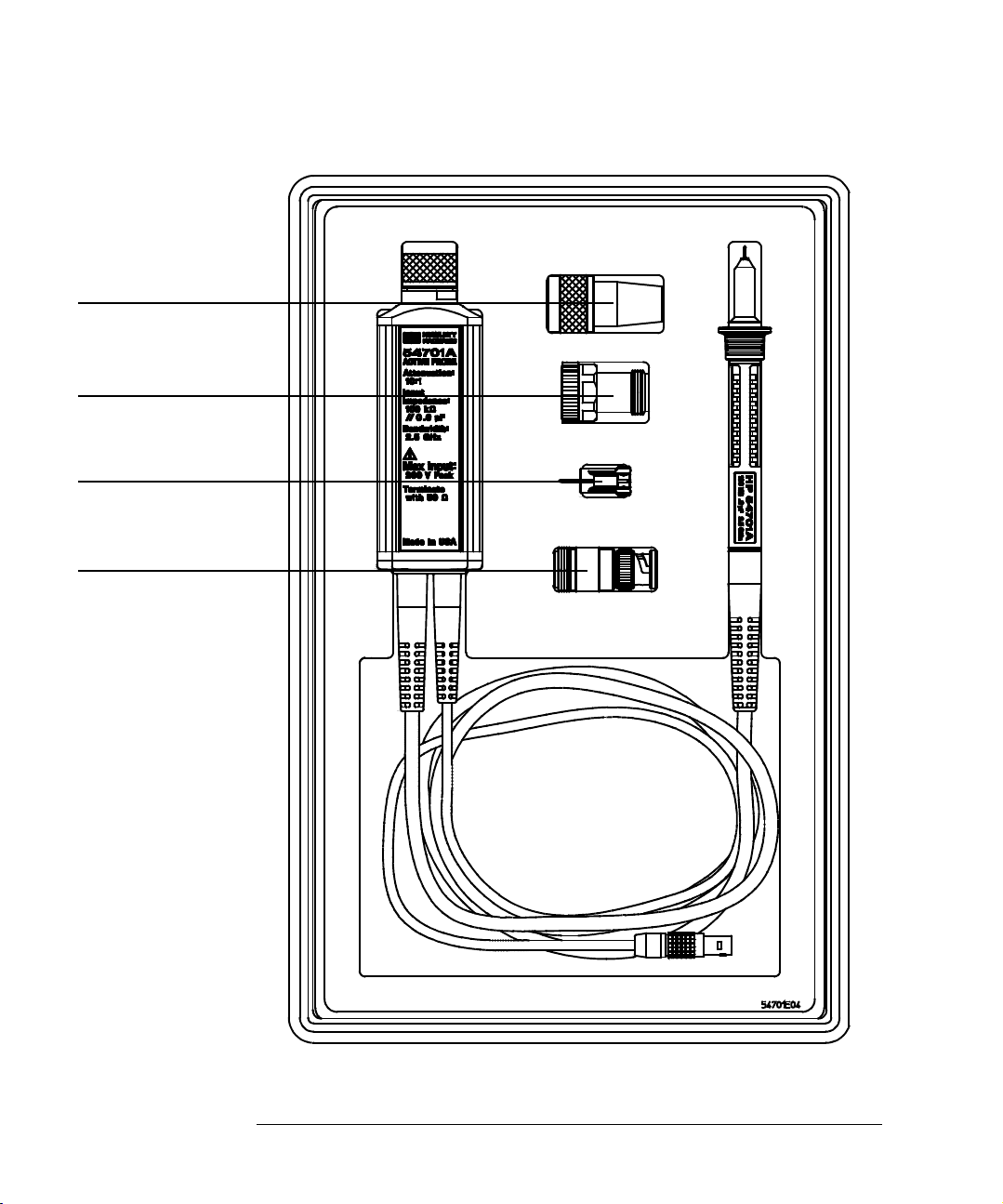
Figure 1
11880A, Type-N(m) to
Probe Adapter
(not supplied, order
separately)
5081-7722A, Type-N(m)
to APC 3.5(f) Adapter
(supplied as Option 001,
or order separately)
Walking-stick Ground
(supplied)
N(f) to BNC(m) Adapter
(supplied)
Chapter 1: Operating the Probe
Included with the probe is a
box of small accessories. See
Page 16 for a complete list of
accessories.
54710A Active Probe
8
Page 9

Chapter 1: Operating the Probe
Introduction
This chapter shows you how to connect and operate the 54701A Active Probe.
The following information is covered in this chapter:
• Inspection
• Probe operating range
• Connecting the probe
• Operating the probe with oscilloscope power
• Operating the probe with a power module
• Using accessories
To inspect the probe
❏ Inspect the shipping container for damage.
Keep a damaged shipping container or cushioning material until the
contents of the shipment have been checked for completeness and the
instrument has been checked mechanically and electrically.
❏ Check the accessories.
Accessories supplied with the instrument are listed in "Accessories
Supplied" in table 1, page 16 in this manual.
• If the contents are incomplete or damaged notify your Agilent
Technologies sales office.
❏ Inspect the instrument.
• If there is mechanical damage or defect, or if the instrument does not
operate properly or pass calibration tests, notify your Agilent
Technologies sales office.
• If the shipping container is damaged, or the cushioning materials show
signs of stress, notify the carrier as well as your Agilent Technologies
sales office. Keep the shipping materials for the carrier's inspection.
The Agilent office will arrange for repair or replacement at Agilent
Technologies’ option without waiting for claim settlement.
9
Page 10

Figure 2
Chapter 1: Operating the Probe
Probe Operating Range
Probe Operating Range
Figure 2 shows the maximum input voltage for the active probe as a function
of frequency. This is the maximum input voltage that can be applied without
risking damage to the probe.
Figure 3
Maximum Input Voltage vs Frequency
Figure 3 shows the operating range of the probe. For the most accurate
measurements and safety for the probe, signals should be within the indicated
operating region.
Area of Optimum
Operating
Probe Operating Range
10
Page 11
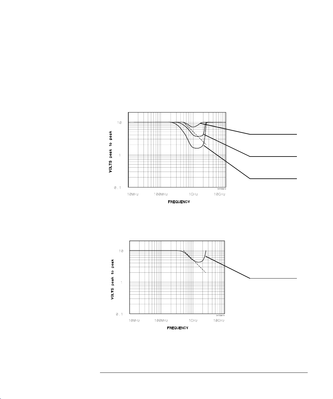
Figure 4
Chapter 1: Operating the Probe
Probe Operating Range
The curves in figures 4 and 5 represent the typical input signal limits for
several levels of second and third harmonic distortion in the output signal. For
input signals below a given curve, the level of harmonic distortion in the
output is equal to or below that represented by the curve. The dashed
straight line in each figure represents the operating range limit as shown in
figure 3 on the previous page.
Second Harmonic
≤ -20 dBc
Second Harmonic
≤ -30 dBc
Second Harmonic
≤ -40 dBc
Figure 5
Second Harmonic Distortion, Input Voltage vs Frequency
Third Harmonic
≤ -40 dBc
Third Harmonic Distortion, Input Voltage vs Frequency
11
Page 12

Chapter 1: Operating the Probe
Probe Operating Range
To connect the probe
1 Connect the probe output to the instrument input.
The probe output is through a Type-N connector and the probe is designed to
be terminated with 50 Ω 1%.
• If your instrument has a fixed 50-Ω input, connect the probe output.
• If your instrument has selectable input resistance, connect the probe
output and set the instrument input resistance to 50 Ω. If your
oscilloscope has probe power for this probe, it may automatically set the
input resistance to 50 Ω for you.
• If your instrument does not provide a 50-Ω input, connect a Type-N(f) to
BNC(m) adapter and a 50-Ω feedthrough (such as an 10100C) to the
output of the probe. Then, connect the probe to the input of your
instrument.
2 Connect the probe power cable to a Power connector.
Red dots on the cable connector housing align with the connector keys. Align
the keys when inserting the cable connector into the power connector.
CAUTION: The probe power cable connector automatically locks in the mating power
connector. To separate the connectors, you must pull on the knurled part of
the cable connector housing. This releases the lock. If you pull on the cable
the connectors won't release and you may damage the connector or cable.
• If your oscilloscope has the appropriate probe power connector, connect
the probe power cable.
Some oscilloscopes have more than one channel, or signal channels with
separate trigger inputs. In these instruments, a probe power connector
may be associated with a specific input. Be sure to connect the probe
power cable to the correct connector so the instrument will respond
correctly to the presence of the probe.
• If your instrument does not have the appropriate probe power connector,
connect the probe power cable to one of the connectors on the 1143A
Probe Offset Control and Power Module. The 1143A provides probe power
and offset control for two probes.
12
Page 13

Chapter 1: Operating the Probe
Probe Operating Range
3 Calibrate the oscilloscope and probe combination with the instrument
calibration routines.
Some oscilloscopes allow you to calibrate the probe as part of the input signal
path. Consult the oscilloscope User Guide for further information.
• If calibrating the probe with the 54700 family oscilloscope, you must
calibrate the plug-in with the mainframe before calibrating the probe with
the system. Use the following procedure:
a. Calibrate the oscilloscope using the best accuracy procedure.
b. Calibrate the probe with the oscilloscope using the probe calibration
procedure.
When the probe has been calibrated with the 54700 system, the dc
gain, offset zero, and offset gain will be calibrated. The degree of
accuracy specified at the probe tip is dependent on the 54700 system
specifications.
• If using an 1143A power module for probe power, set the Offset controls to
Local and Zero while performing the calibration. Follow the calibration
procedures for your oscilloscope.
CAUTION: An effort has been made to design this probe to take more than the average
amount of physical and electrical stress. However, with an active probe, the
technologies necessary to achieve high performance do not allow the probe to
be unbreakable. Treat the probe with a moderate amount of care. It can be
damaged if it is dropped from excessive heights onto a hard surface.
Connecting the probe to the 54120 family oscilloscopes
There are a few things to consider when connecting the 54701A Active Probe
to one of the 54120 family of high performance oscilloscopes.
• Use the special Type N(f) to APC 3.5(f) bulkhead adapter to connect the
probe output to the input of the test set. The adapter provides the full
bandwidth and pulse fidelity of the probe as well as full mechanical
support. The use of other adapters can compromise signal fidelity and
may be vulnerable to mechanical damage.
13
Page 14

Chapter 1: Operating the Probe
Probe Operating Range
The Type-N(f) to APC 3.5(f) adapter can be ordered with the probe as
Option 001 or ordered separately, part number 5081-7722.
• The dynamic range of the system will be 3.2 V (6.4 Vp-p) which, with
probe offset, covers most digital technologies.
Using the probe with oscilloscope power
Probe power and offset control are provided by the oscilloscope. There are
several factors to consider about the oscilloscope and probe combination.
• IThe oscilloscope recognizes the presence and type of probe and adapts
the vertical scale factors to reflect the probe characteristics.
• The offset function is transferred to the probe but this is transparent to the
user. The offset will be limited to a range acceptable to the probe. With
54700 family of oscilloscope plug-ins, the offset range is 50 V. See the
sidebar below.
• Since the 54701A is an active probe, the bandwidth of the oscilloscope and
probe combination is a mathematical combination of their individual
specifications.
Equation 1 System Bandwidth =
where
tr1 is the risetime of the oscilloscope.
tr2 is the risetime of the probe
If you are using a 54700 family oscilloscope, the resultant bandwidth with a
specific mainframe, plug-in, and probe combination is noted on a sticker
on the side panel of the plug-in
The probe has limiting designed to avoid excessive power dissipation. The input
operating range of the probe is 5 V. If the input and offset exceeds +14V relative
to the probe tip, the output of the probe will limit at +1.4 V. As the input plus
offset reaches -14 V, the output will limit at -1.4 V; then, it will fold back to
approximately -0.8V as the input plus offset exceeds -14 V. The output of the
probe will remain at the limit voltage until the input plus offset falls below
approximately -8 Vdc.
14
0.35
------------- ------------- ------------- --
2
tr1()
+
tr2()
2
Page 15

Chapter 1: Operating the Probe
Probe Operating Range
Using the probe with the 1143A power module
Probe power and offset control is provided by the 1143A Probe Offset Control
and Power Module.
1 Set up the power module by following the instructions in the User and
Service Guide.
2 Connect the probe using “To connect the probe” on page 12" of this
guide.
3 Turn on the power for the power module.
4 Set the appropriate Remote/Local switch.
• To control offset voltage with the power module, set the switch to
Local.
• To control the offset voltage remotely, set the switch to Remote.
5 With Local control, set the appropriate Zero/Variable switch.
• To enable the local offset control, set the switch to Variable.
• To disable the local offset control, set the switch to Zero.
6 Connect the probe to the signal to be measured.
If the oscilloscope has an offset feature, be sure that it is set to zero so
that the probe offset does not have to compensate for the oscilloscope
offset.
7 If necessary, adjust the Coarse and Fine offset controls so the desired
part of the signal is displayed on the oscilloscope. See sidebar below.
The offset range is greater than 50 V relative to the probe tip.
Bandwidth issues are the same as covered on the previous page
The probe has limiting designed to avoid excessive power dissipation. The input
operating range of the probe is 5 V. If the input and offset exceeds +14V relative
to the probe tip, the output of the probe will limit at +1.4 V. As the input plus
offset reaches -14 V the output will limit at -1.4 V; then, it will fold back to
approximately -0.8V as the input plus offset exceeds -14 V. The output of the
probe will remain at the limit voltage until the input plus offset falls below
approximately -8 Vdc.
See Also The User and Service Guide for the 1143A Probe Offset Control and Power
Module about remote probe operation.
15
Page 16
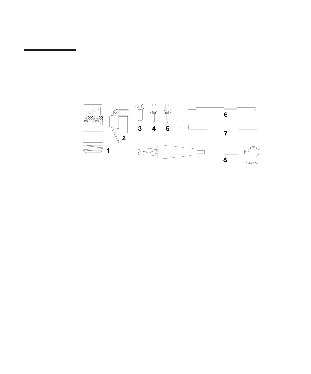
Figure 6
Table 1
Chapter 1: Operating the Probe
Probe Operating Range
Using probe accessories
The following figure and table illustrate the accessories supplied with the
54701A Active Probe.
Accessories Supplied
Item Description Qty Part Number
1 Type-N(f) to BNC(m) adapter 1 1250-0077
2 Walking-stick ground 1 5960-2491
3 Single contact socket 5 1251-5185
4 Standard probe pin 5 54701-26101
5 Sharp probe pin 2 5081-7734
Nut Driver 3/32-in (not shown) 1 8710-1806
6 200-Ω signal lead 1 54701-81301
7 Ground extention lead 1 0650-82103
8 Alligator ground lead 1 01123-61302
* Flexible Probe Adapter 1 54701-63201
* Probe Socket 1 5041-9466
* Coaxial Socket 3 1250-2428
Operating and Service Guide 1 see title page
* These parts are illustrated on pages 18 and 19.
16
Page 17

Chapter 1: Operating the Probe
Probe Operating Range
Type-N to BNC Adapter
The Type-N(f) to BNC(m) adapter connects the output of the probe to
instruments with a BNC input. If the instrument input does not have a 50-Ω
termination, use an adapter with an integral 50-Ω load or add a 50-Ω
feedthrough (10100C) between the adapter and instrument input.
Walking-stick Ground
The walking-stick ground is the best ground for general probing. It is short,
and the ground wire includes a bead for damping probe resonance. This
provides a well maintained probe response for frequencies to 2.5 GHz.
Single Contact Socket
The single contact sockets can be soldered into a circuit to provide a probe
point to hold the probe tip or ground. The socket accepts 0.018-inch to 0.040inch pins. The sockets accept the probe tips, the walking-stick ground, the
200-Ω signal lead, and the ground extention lead.
Probe Pins
There are two types of replaceable probe pins furnished with the probe. The
0.030-inch round standard probe pin is for general applications. It is made of a
material that will generally bend before breaking. The 0.025-inch round sharp
probe pin has a narrower point and is a harder material. It can be used to
probe constricted areas or penetrate hard coatings.
CAUTION: Do not solder the probe tip into circuitry. Excessive heat may damage the tip
or circuitry inside the probe. If you need to solder something into your
circuitry, use the single contact sockets, ground extention lead, or 200-Ω
signal lead. They are less easily damaged and less expensive to replace.
• To remove and replace probe pins, use the nut driver to unscrew the tip
from the end of the probe.
• Be sure to screw the replacement tip all the way in or the probe may be
intermittent or appear ac coupled.
Nut Driver
The 3/32-in nut driver is provided for easier replacement of the probe tips.
17
Page 18

Chapter 1: Operating the Probe
Probe Operating Range
200-Ω Signal Lead
This 2-inch orange extention lead includes a molded-in resistor to dampen
resonance caused by the lead inductance. Use this lead and the ground
extention lead to provide a flexible connection to the circuit under test.
There is a tradeoff when using the extention leads. To maintain a clean pulse
response, the probing system bandwidth is limited to 1.5 GHz. Probe
resonance is damped by the walking-stick bead and the resistor in the signal
lead.
Ground Extention Lead
This 2.25-inch black ground lead can be used to extend ground from the
walking-stick to the circuit under test. When used with the walking-stick
ground the probe resonance is damped by the bead on the walking-stick.
Alligator Ground Lead
The alligator ground lead can be used in general applications when the
bandwidth of the signal is 350 MHz or lower. With no signal lead extention the
probe resonant frequency is about 650 MHz.
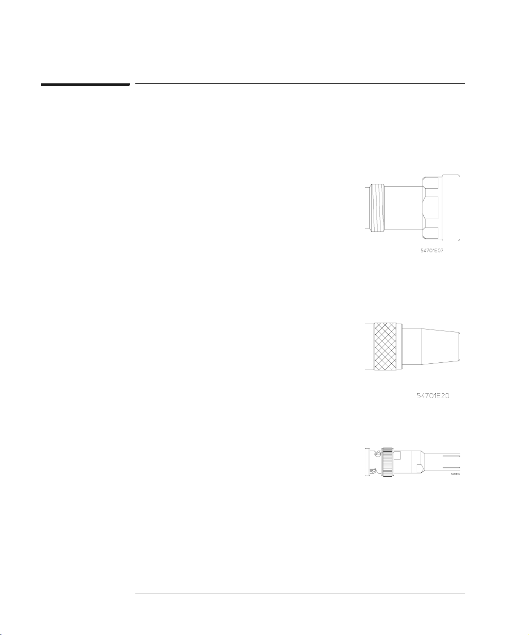
Flexible Probe Adapter
The flexible probe adapter provides a
high-quality connection between a
coaxial socket and the 54701A probe.
The right-angle connection allows the
probe to remain parallel to a PC board
and the flexibility prevents the leverage
of the probe and cable from damaging PC
board circuitry.
As with any cable-type interconnection,
always apply insertion and removal forces
to the connectors directly, and not
through the cable itself (see the
illustration).
18
Page 19

Probe Socket
The probe socket is a direct fit to the
shield surface of the 54701A probe.
Use this socket and the single contact
socket to design the highest quality
probing of a PC board. The
illustration shows the socket and the
PC board layout needed to mount the
parts.
Coaxial Socket
The coaxial socket is designed to fit the
standard mini-probe. When used with the
flexible probe adapter, it can be installed in a
circuit so you can probe with the 54701A.
The illustration shows the socket and the PC
board layout needed to mount the socket to
the board.
Chapter 1: Operating the Probe
Probe Operating Range
Probe socket
Single contact
socket
See Also Chapter 2, "Probing Considerations," for a more complete discussion about the
effects of probe connection techniques on signal fidelity.
See Also "Replaceable Parts" chapter 3 for replacement parts that are available but not
listed here.
19
Page 20
Chapter 1: Operating the Probe
Probe Operating Range
Additional Accessories
The following accessories enhance use of the active probe. For ordering
information, see "Replaceable Parts" in chapter 3.
Type-N to APC 3.5 Adapter
The Type-N(f) to APC 3.5(f) bulkhead adapter is an
optional adapter (Option 001, part no. 5081-7722)
specifically designed to connect the active probe to
the input of the 54120 family of high-performance
oscilloscopes. The adapter provides the full
bandwidth and pulse fidelity of the probe as well as
full mechanical support. The use of other adapters
can compromise signal fidelity and may be
vulnerable to mechanical damage. This adapter can
be ordered with the probe as Option 001.
Type-N to Probe Tip Adapter
The 11880A Type-N(m) to probe tip adapter is
available to connect the input of the active probe to
Type-N connectors. It has an internal 50-Ω load. It
can be used for general testing and is specifically
recommended for testing the probe bandwidth.
This adapter must be ordered separately.
BNC to Probe Tip Adapter
The 10218A BNC(m) to probe tip adapter is
available to connect the input of the active probe to
BNC type connectors. It does not have an internal
load so it is not recommended for testing where the
full bandwidth of the probe is needed. This adapter
must be ordered separately.
20
Page 21

2
Probing Considerations
21
Page 22

Chapter 2: Probing Considerations
Introduction
This chapter gives you some guidance about the effects of probing and how to
get the best measurement results. The effect of the following parameters are
covered in this chapter:
• Resistive Loading
• Capacitive Loading
• Ground Inductance
• Bandwidth
Two important issues while measuring signals with probes are how the probe/
oscilloscope combination represents the signal at the probe tip and how the
probe affects the circuit during the measurement.
When a probe is connected to a circuit to measure a signal it becomes part of
the circuit. Probing a signal can be easy and successful if some forethought is
given to the nature of the circuit under test and what type of probe best solves
the measurement problem. Because of the wide variety of signals that may be
encountered, ranging from high bandwidth (fast rise times) to high
impedance, in a given situation one probe may do a better job than another.
Therefore, it is helpful to understand the different effects caused by the
interaction between the probed circuit and the probe.
22
Page 23

Figure 7
Wavefo rm 1
Chapter 2: Probing Considerations
Resistive Loading Effects
Resistive Loading Effects
The two major effects caused by resistive loading are amplitude distortion and
changes in dc bias conditions in the circuit under test.
Amplitude Distortion
Amplitude distortion is depicted in figure 7, where waveform 1 is the signal
before probing and waveform 2 is the signal while probing. (The baselines of
these signals have been overlayed to show the amplitude change. If the
baseline of a signal is not at zero volts it will shift when the signal is probed.)
Wavefo rm 2
Oscilloscope Display Showing Amplitude Distortion
The cause of the error is the voltage divider developed between the source
resistance of the device under test and the input resistance of the probe being
used. Equation 2 calculates the error caused by the voltage divider.
Equation 2 Error(%) =
A probe with an input resistance ten times that of the source resistance of the
device under test causes a 9.09% error in the measurement. It is best to use a
probe with an input resistance at least ten times that of the source resistance.
R
source
------------- ------------- -------------- 1 0 0×
R
+
sourceRprobe
23
Page 24

Figure 8
Chapter 2: Probing Considerations
Resistive Loading Effects
Bias Changes
Probes with low input resistance can cause bias changes in the device under
test. A good example of this effect can be seen when probing ECL circuits.
Figure 8 represents a typical ECL node with a 60-Ω bias resistor to -2 V. Ip
represents current that flows from ground into the circuit when the probe is
connected. The table shows the current that flows in each device at both the
high (-0.8 V) and low (-1.75 V) states, with and without a 500-Ω probe
connected.
High (-0.8 V) Low (-1.75 V)
Without
Probe
I
20 mA 18.4 mA 4.2 mA 0.7 mA
O
I
20 mA 20 mA 4.2 mA 4.2 mA
R
I
P
With
Probe
1.6 mA 3.5 mA
Without
Probe
With
Probe
Probing ECL Circuits
Note that in the high state there is little difference in current flow with or
without the probe connected. However, in the low state the output stage is
closer to cutoff. Connecting the probe sources current into the output node,
which reduces the current sourced from the gate output. The output current
drops from 4.2 mA to 0.7 mA. The low output current can cause problems
with switching noise margins. The output gate will have difficulty reaching
the low threshold, so ac performance will suffer because the falling edge
degrades. If a larger bias resistor had been used to keep the current levels
lower, when a 500-Ω probe is attached the output gate could go into cutoff
before it reaches the low threshold.
Recommendation
Be careful not to use a probe just because it has the highest input resistance
available. High-resistance probes usually come with trade-offs in other
important parameters, such as higher capacitance, which also affect
measurement accuracy.
24
Page 25

Figure 9
1 MΩ/6pF probe
Chapter 2: Probing Considerations
Resistive Loading Effects
Capacitive Loading Effects
The input capacitance of a probe causes the overall input impedance to
decrease as a function of frequency. For this reason, input capacitance
becomes one of the most important parameters that affect high frequency
measurements. Figure 9 plots the probe impedance vs frequency for two
probes: a 1-MΩ, 6-pF probe and the 54701A probe (100 kΩ, 0.6 pF). It shows
that because of the lower input capacitance, the 54701A probe actually has a
higher input impedance for frequencies above 240 kHz. At frequencies above
2.65 MHz, it has as much as 10 times the impedance of the 1-MΩ probe.
54701A probe
Probe Impedance vs Frequency
The input capacitance of a probe forms an RC time constant with the parallel
combination of source impedance and probe input resistance. This can cause
an increase in the circuit rise time and a time delay in a pulse edge.
25
Page 26

Figure 10
Plot 1
Plot 2
Plot 3
Chapter 2: Probing Considerations
Resistive Loading Effects
Figure 10 represents plots from three spice simulations showing this loading
effect. Plot 1 shows the signal edge before probing. Plot 2 shows the edge
after probing with a 6-pF probe and plot 3 after probing with a 15-pF probe.
Table 2
Spice Simulation Of Probe Capacitance Loading Effects
Table 2 summarizes the data. It shows that the 6-pF probe didn't significantly
increase the rise time of the signal, but delayed it (referenced at the 50%
point) approximately 150 ps. The 15-pF probe not only slowed the rise time
approximately 33% but also delayed the edge 340 ps.
Probe Capacitance Loading Effect
Plot Risetime Delay
1 1 ns 0.0 ps
2 1.067 ns 150 ps
3 1.33 ns 340 ps
26
Page 27

Chapter 2: Probing Considerations
Resistive Loading Effects
Ground Inductance Effects
Probe grounding techniques are an important factor in making accurate high
frequency measurements. The main limitation, probe resonance, is a function
of the input capacitance of the probe and the inductance of the ground return.
These two parameters in series form an LC resonant circuit that, when
connected to the circuit under test, becomes part of the circuit's response.
The probe resonance can cause overshoot and ringing on pulse edges that
contain energy in the same frequency band as the resonance. The true
response is masked, the false response gets transferred to the oscilloscope,
and the oscilloscope display shows an incorrect result. If overshoot and
ringing added by a probe during troubleshooting changes how the circuit
functions, it can produce an incorrect judgment about circuit operation.
To minimize the problem of ground ringing, use the shortest possible ground
with a probe that has the lowest possible input capacitance. Equation 3 can
be used to calculate the frequency where a certain probe and grounding
technique resonates.
Equation 3 f
1
=
------------- ------
r
2π LC
where
C is the probe input capacitance. (It is usually found in the probe data
sheet.)
L is the inductance of the ground return. (It can be approximated
using the constant of 25 nH per inch.)
Figure 11 plots the probe impedance vs frequency for two probes: a 1-MΩ, 6-
pF probe and the 54701A probe (100 kΩ, 0.6 pF). It also plots the inductive
reactance vs frequency for three different values of ground inductance. The
5-nH inductance represents a PC board socket, the 20-nH inductance a
spanner ground, and the 100-nH inductance a 4-inch ground wire. Where the
probe plots cross the inductance plots gives the resonant frequency of the
probe and ground combination. You can see from the graphs that in all three
cases the 6-pF probe resonates at approximately one-third the frequency of
the 54701A (0.6 pF). The lower resonance means that the effect of the
resonance is more likely to influence the representation of the signal.
27
Page 28

Figure 11
1-MΩ, 6-pF probe
1-MΩ, 6-pF probe
Chapter 2: Probing Considerations
Resistive Loading Effects
Probe Impedance and Resonance
28
Page 29

Figure 12
Wavefo rm 1
Wavefo rm 2
Wavefo rm 3
Wavefo rm 4
Chapter 2: Probing Considerations
Resistive Loading Effects
Figure 12 shows waveforms measured by the 54701A (100 kΩ, 0.6 pf) and the
1-MΩ, 6-pF probe; both probes are connected to a 1-GHz oscilloscope.
Probe Resonance Effects
Waveform 1 shows the pulse response of a 6-pF probe measuring a 400-ps
step. The ringing on the pulse is caused by the input capacitance of the probe
and by the inductance of the ground return. The period of the ringing
measures 1.72 ns, representing a frequency of 581 MHz. The circuit had a
ground return of 1/2 inch. Using equation 3 to calculate the resonant
frequency (12.5 nH and 6 pF) results in 580 MHz. The measurement and the
calculation yield the same result, showing how probe resonance causes
problems when probing high speed signals.
Waveform 2 shows the pulse response when the same 6-pF probe measures an
800-ps edge. Notice that the overshoot and ringing are still present, but are
significantly reduced. This is because the slower signal edge has less energy
at the resonant frequency of the probe.
Waveform 3 shows the pulse response when the 6-pF probe measures a 1.25ns edge. The ringing is nearly subdued and doesn't play a significant role in
the measurement.
Waveform 4 shows the 54701A 0.6-pF probe, with a one-inch ground lead,
measuring the 400-ps edge. Because of its much lower capacitance, and even
with a longer ground lead, its resonant frequency is much higher and it shows
no ringing in the response.
29
Page 30

Chapter 2: Probing Considerations
Resistive Loading Effects
The measurements from the first three waveforms lead to a rule of thumb:
To minimize signal distortion due to probe resonance, provide a two-to-one, or
greater, difference between the resonant frequency of the probe and the
bandwidth of the signal being measured.
For pulsed data applications, the rise time of a signal can be related to the
bandwidth by using a constant of 0.35 as shown in equation 4. This equation is
derived from a first order RC response.
Equation 4 Bandwidth =
0.35
----------
t
r
Example The 1.25-ns edge (waveform 3 in figure 12) equates to a 280-MHz bandwidth.
Bandwidth =
0.35
----------
t
r
0.35
------------- -----------280MHz==
1.25
×10
-9
This is approximately half the resonant frequency calculated for the 6-pF
probe with 1/2-inch ground, 580 MHz. Therefore the subdued ringing on
waveform 3 validates the rule of thumb.
As noted before, waveform 4 shows the effect when a low-capacitance probe
measures a high-frequency signal. Because of the low capacitance the
resonant frequency is high. Therefore, there is less chance of the probing
system affecting the measurement of the signal.
30
Page 31

Chapter 2: Probing Considerations
Resistive Loading Effects
Probe Bandwidth
The bandwidth of the probe is often given much consideration during
purchase, then forgotten while making measurements. Error in
measurements occur when the frequency content (at the -3 dB point) of the
signal being measured approaches or exceeds the bandwidth of the probe.
The probe can be modeled as a low-pass filter for the signal.
Example
Equation 5 ,
If a 700-MHz probe is used to measure a 1-ns signal, the rise time error can be
calculated using equations 4 and 5. For this exercise assume that the oscilloscope
bandwidth is great enough not to contribute any errors.
t
r
where
tr1()2tr2()
t
1 is the rise time of the probe,
r
t
2 is the rise time of the signal.
r
2
+=
1. Calculate the rise time of the 700-MHz probe (equation 4).
t
r
0.35
------------ ------------- ---Bandwidth
2. Calculate the rise time of the 1-ns signal as measured by the 700-MHz
probe (equation 5).
0.5()21.0()
t
r
The measurement error between the actual signal and what was measured is 12%.
To keep measurement errors less than 6%, use a probe with a band- width three or
more times that of the signal.
+ 1.25 1.12ns===
3. Calculate the bandwidth of the 1-ns signal (equation 4).
Bandwidth
0.35
---------- 3 5 0 M H z==
1ns
0.35
------------ ----------0.5ns===
700MHz
2
Use a probe with a bandwidth of 1.05 GHz (the rise time is 0.333 ns, equation 4).
4. Calculate the rise time of the 1-ns signal measured by the 1.05-GHz probe
(equation 5).
t
0.333()21.0()
r
Now, the measurement error is less than 6%.
2
+ 1.11 1.054ns===
31
Page 32

Chapter 2: Probing Considerations
Resistive Loading Effects
Conclusion
In conclusion we can review the issues by using the effect the 54701A Active
Probe (100 kΩ, 0.6 pF) has while measuring a fast CMOS gate.
Resistive Loading
Resistive loading is caused by the input resistance of the probe. When the
CMOS output is high (5 V) the 100 kΩ input resistance of the probe draws 50
mA. A CMOS gate can drive many times this current, so the load is
insignificant. In addition, the output impedance of a CMOS gate is the on
resistance of the output FET. Whether high or low, this is typically less than
100 Ω. The voltage divider of 100 Ω and 100 kΩ is also insignificant and will
not change the value of either state of the gate.
Capacitive Loading
CMOS gates typically have an input capacitance between 5 and 10 pF. The
traces between gates will contribute another 5 to 10 pF, which gives a total of
10 to 20 pF. The 0.6-pF input capacitance of the 54701A probe is about 3% to
6% that of the circuit capacitance. It will not significantly change the time
constant in the node being probed.
Ground Inductance
The CMOS gate has a risetime approaching 1 ns. This equates to a bandwidth
of 350 MHz (equation 4). If we use the walking-stick ground (about 20 nH)
provided with the 54701A probe, the probe resonance will be about 1.45 GHz
(equation 3). We can see that the CMOS equivalent bandwidth (350 MHz) is
at less than half the resonant frequency of the probe. This fits within the rule
of thumb given previously, that to avoid ringing in the response, the resonance
of the probe should be at least twice the frequency of the energy in the signal.
Bandwidth
Although it was specifically not covered in this chapter, the bandwidth of the
probe and oscilloscope combination is also very important. As previously
noted, with CMOS signals of 1 ns risetimes the signal bandwidth is 350 MHz.
This means for an accurate representation the probe and oscilloscope
combination should have at least a 3-to-1 margin in bandwidth, at least
1.05GHz.
32
Page 33

3
Service
33
Page 34

Chapter 3: Service
Introduction
This chapter provides service information for the 54701A Active Probe. The
following sections are included in this chapter:
• Specifications and Characteristics
• Returning for Service
• Calibration Testing Procedures
• Making Adjustments
• Troubleshooting and Repair
34
Page 35

Table 3
Chapter 3: Service
General Information
General Information
The following general information applies to the 54701A 2.5 GHz Active
Probe.
Specifications
Table 3 gives specifications used to test the active probe.
Specifications
Attenuation Factor 10:1
Bandwidth (-3dB) >2.5 GH
dc Gain Accuracy ±0.5%
Input Resistance 100 kΩ 1%
35
Page 36

Table 4
Chapter 3: Service
General Information
Characteristics
Table 4 gives characteristics that are typical for the active probe.
Characteristics
Rise time* <140 ps
Input Capacitance 0.6 pF (typical)
Maximum Input Voltage ±200 V[dc + peak ac(<20 MHz)]
ESD Tolerance
(150 Ω/150 pF)
±12 kV
Flatness
<3 ns from rising edge ±6%
3 ns from rising edge
(for input edge 170 ps)
Dynamic Range
(<1.5% gain compression)
Offset Adjustment Range
(referenced to the probe tip)
±1%
±5 V peak ac and 50 Vdc
±50 V
Offset Accuracy ±1% of offset 1 mV
Offset Gain
(referenced to the probe tip)
RMS Output Noise (
loaded by 50 Ω
)
dc to 2.5 GHz, input
11.5 V/mA
<300 mV
Propagation Delay 7.5 ns (approximately)
* Risetime figure calculated from tr = 0.35/Bandwidth
36
Page 37

Table 5
Chapter 3: Service
General Information
General Characteristics
The following general characteristics apply to the active probe.
General Characteristics
Environmental Conditions
Operating Non-operating
Temperature 0°C to +55 C° (32°F to +131°F) -40°C to +70°C (-40°F to +158°F)
Figure 13
Humidity up to 95% relative humidity (non-
condensing) at +40°C (+104°F)
Altitude up to 4,600 meters (15,000 ft) up to 15,300 meters (50,000 ft)
Vibration Random vibration 5 to 500 Hz, 10
minutes per axis, 0.3grms.
Power
Requirements
Weight Net: approximately 0.6 kg (1.3 lb)
Dimensions Refer to the outline drawings below.
±17 Vdc and -17 Vdc at 110 mA each (+16.5 Vdc and -16.5 Vdc
minimum respectively)
Shipping: approximately 1.0 kg (2.3 lb)
up to 90% relative humidity at
+65°C (+149°F)
Random vibration 5 to 500 Hz,
10 min. per axis, 2.41 grms.
Resonant search 5 to 500 Hz
swept sine, 1octave/min.
sweep rate, (0.75g), 5 min.
resonant dwell at 4 resonances
per axis.
Mechanical Dimensions
37
Page 38

Chapter 3: Service
General Information
Product Regulations
Safety IEC 348
UL 1244
CSA-C22.2 No.231 (Series M-89)
EMC This product meets the requirement of the European Communities (EC)
EMC Directive 89/336/EEC.
Emissions EN55011/CISPR 11 (ISM, Group 1, Class A equipment)
SABS RAA Act No. 24 (1990)
Immunity EN50082-1
Code
1
Notes
IEC 801-2 (ESD) 4 kV CD,8kV AD 1
IEC 801-3 (Rad.) 3 V/m 1
IEC 801-4 (EFT) 1kV 1
1
Performance Codes:
2
1PASS - Normal operation, no effect.
2PASS - Temporary degradation, self recoverable.
3PASS - Temp. degradation, operator intervention required.
4FAIL - Not recoverable, component damage.
2 Notes:
(None)
Recommended Test Equipment
The table on the next page is a list of the test equipment required to service
this instrument. The table indicates the critical specification of the test
equipment and for which procedure the equipment is necessary. Equipment
other than the recommended model may be used if it satisfies the critical
specification listed in the table.
38
Page 39

Table 6
Chapter 3: Service
General Information
Recommended Test Equipment
Equipment
Required
Signal Generator 50 MHz to 2.5 GHz 8663A C
Power Meters (2)
or one DualChannel
Power Sensor (2 50 MHz to 2.5 GHz, 300 mW 8482A C
Power Splitter dc to 2.5 GHz, ≤0.2 dB output tracking,
Power Supply Power and control for probe under test 1143A C,A,T
DVM Resistance ±0.1,% Volts and ohms
Power Supply 5 Vdc 6114A C
Adapter/termination N(f)-to-probe, 50 Ω 11880A C
Adapter N(f-f), 50 Ω 1250-1472 C
Adapter N(f)-to-BNC(m), 50 Ω 1250-0077 C,A,T
Termination 50 Ω, BNC feed-through 10100C C,A,T
Adapter BNC (f) to banana (m 1251-2277 C
C = CalibrationTests, A = Adjustments, T = Troubleshooting
Critical Specifications
50 MHz to 2.5 GHz,
±3% accuracy
Type-N
±0.01%
Recommended
Model/Part
436A (2),
437A (2), or
438A (1)
11667A C
3458A C,A,T
Use
C
Service Strategy
The 54701A Active Probe is a high-frequency instrument with many critical
relationships between parts. For example, the frequency response of the
amplifier on the hybrid is trimmed to match the output coaxial cable. As a
result, to return the probe to optimum performance requires factory repair. If
the probe is under warranty, normal warranty services apply. If the probe is
not under warranty, a failed probe can be exchanged for a reconditioned one
at a nominal cost.
See Also "Troubleshooting and Repair" for further information.
39
Page 40

Chapter 3: Service
General Information
To clean the instrument
Use mild soap and water to clean the instrument. Harsh soaps will damage the
water-based paint finish of the instrument.
To return the probe to for service
Before shipping the instrument to Agilent Technologies, contact your nearest
Agilent sales office for additional details.
1 Write the following information on a tag and attach it to the instrument.
• Name and address of owner
• Instrument model number
• Instrument serial number
• Description of the service required or failure indications
2 Remove all accessories from the instrument.
Accessories include all cables. Do not include accessories unless they are
associated with the failure symptoms.
3 Protect the instrument by wrapping it in plastic or heavy paper.
4 Pack the instrument in foam or other shock absorbing material and
place it in a strong shipping container.
You can use the original shipping materials or order materials from an Agilent
Technologies Sales Office. If neither are available, place 3 to 4 inches of
shock-absorbing material around the instrument and place it in a box that
does not allow movement during shipping.
5 Seal the shipping container securely.
6 Mark the shipping container as FRAGILE.
In any correspondence, refer to instrument by model number and full serial
number.
40
Page 41

Chapter 3: Service
Calibration Testing Procedures
Calibration Testing Procedures
The calibration procedures in this section are used to determine if the 54701A
meets the designated warranted specifications.
Testing Interval
The calibration test procedures may be performed for incoming inspection of
the instrument and should be performed periodically thereafter to ensure and
maintain peak performance. The recommended test interval is yearly or every
2,000 hours of operation. Amount of use, environmental conditions, and the
user's experience concerning need for testing will contribute to verification
requirements.
The calibration cycle is covered in the "Making Adjustments" section in this
chapter.
Equipment Required
A complete list of equipment required for the calibration tests is in the
Recommended Test Equipment table on page 41. Equipment required for
individual tests is listed in the test. Any equipment satisfying the critical
specifications listed may be substituted for the recommended model.
Test Record
The results of the calibration tests may be tabulated on the Test Record
provided at the end of this section on page 50. The Test Record lists the
calibration tests and provides an area to mark test results. The results
recorded in the table at incoming inspection may be used for later
comparisons of the tests during periodic maintenance, troubleshooting, and
after repairs or adjustments.
41
Page 42

Chapter 3: Service
Calibration Testing Procedures
To test input resistance
This test checks the input resistance of the active probe.
Specification: 100 kΩ 1%
Equipment Required
Equipment Critical Specification
Digital Multimeter Resistance 0.1% 3458A
Recommended
Model/Part
1 Connect the DMM between the probe tip and the ground shell at the
front of the probe.
2 Set up the DMM to measure resistance.
The resistance should read 100 kΩ 1KΩ.
3 Record the reading in the “Calibration Test Record” on page 47.
If the test fails
Go to the "Troubleshooting and Repair" section in this chapter.
42
Page 43

Calibration Testing Procedures
To test dc gain accuracy
This test checks the dc gain accuracy of the probe.
Specification: 0.1 0.5%
Equipment Required
Chapter 3: Service
Equipment Critical Specification
Power Supply 5 Vdc 6114A
Digital Multimeter Better than 0.1% accuracy 3458A
Power Supply Power and control for probe under test 1143A
Adapter N(f)-to-BNC(m) 1250-0077
Termination 50 Ω, BNC feed-through 10100C
Adapter BNC (f) to banana (m) 1251-2277
Recommended
Model/Part
1 Set the power supply for 5.0 V 0.05% (2.50 mV)
Use the DVM to measure the voltage if necessary.
2 Connect the power connector of the active probe to the 1143A Probe
Offset Control and Power Module or an oscilloscope with an
appropriate probe power output.
3 Connect the output of the probe to the input of the DVM using the N-
to-BNC adapter, 50-Ω feedthrough, and BNC-to-banana adapter.
4 Set the probe offset to zero.
If using the 1143A power module, set the Offset controls to Local and Zero.
If using an oscilloscope for probe power, use the channel menu to set the
offset to 0.0 V.
5 Short the input pin of the probe to the shield at the probe tip.
You can use the 11880A (see “To test bandwidth” on page 45.) which is an
Type N-to-probe tip adapter with an internal 50-Ω termination. The objective
is to effectively short the probe input without inducing any signal. Another
method can be used if it meets that requirement.
43
Page 44

Chapter 3: Service
Calibration Testing Procedures
6 Read and record the offset voltage on the DVM. _____________mV
If the offset voltage is greater than 1.0 mV, continue with the test but see the
second sidebar at the end of this test.
7 Connect the probe to the 5.0 V supply.
8 Read and record the voltage reading on the DVM. _____________mV
9 Subtract the reading in step 6 from the reading in step 8.
_____________mV
The result should be 500 mV 2.5 mV.
10 Calculate the dc gain.
result in step 9
------------- ------------- ------------- ---------- --------
5.00 V (supply voltage)
The dc gain should be between 0.09950 and 0.10050 (0.10 0.5%).
11 Record the results of step 10 in the Calibration Test Record on page
50..
If the test fails
Go to the troubleshooting section in this chapter.
.
If the offset voltage is greater than 1.0 mV
If the offset voltage is close to the specification, it should not affect this test. Use
the "Troubleshooting and Repair" section to determine why the offset voltage is
not at zero.
44
Page 45

Chapter 3: Service
Calibration Testing Procedures
To test bandwidth
This test checks the bandwidth of the probe. A high-frequency signal
generator and two power meters are used to set the input and measure the
output of the probe.
Specification: down less than 3 dB, dc to 2.5 GHz
Equipment Required
Equipment Critical Specifications
Signal Generator 50 MHz to 2.5 GHz 8663A
Power Meters (2)
or one DualChannel
Power Sensor (2) 50 MHz to 2.5 GHz, 300 mW 8482A
Power Splitter dc to 2.5 GHz, ≤0.2 dB output tracking,
Power Supply Power and control for probe under test 1143A
Adapter/termination N(f)-to-probe, 50 Ω 11880A
Adapter N(f-f), 50 Ω 1250-0772
Adapter N(m-m), 50 Ω 1250-0078
50 MHz to 2.5 GHz,
±3% accuracy
Type -N
Recommended
Model/Part
436A (2),
437A (2), or
438A (1)
11667A
1 Zero and calibrate the power meters with the power sensors.
2 Connect the equipment as in the figure on the next page.
3 Connect the probe power input connector to the 1143A or oscilloscope
probe power.
4 Set the probe offset to zero.
If using an 1143A power module, set Offset controls to Local and Zero.
If using an oscilloscope for probe power, use the channel menu to set the
offset to 0.0 V.
5 Set the signal generator for 50 MHz at 0.0 dBm.
6 Set the power meter calibration factors to the 50 MHz value on the
power sensors.
45
Page 46

Figure 14
Chapter 3: Service
Calibration Testing Procedures
Bandwidth Test Setup
7 Adjust the signal generator power output for exactly -6.0 dBm as read
on the input power meter.
8 Note the power level reading on the output power meter. 50 MHz
power level _______________ dBm.
The output power level will be approximately -26 dBm. This corresponds to
the 10:1 division ratio of the probe.
9 Change the signal generator frequency to 2.5 GHz.
10 Set the power meter calibration factors to the 2.5 GHz value on the
power sensors.
11 Re-level the signal generator output power for a -6.0 dBm reading on
the input power meter.
12 Note the power level reading on the output power meter. 2.5 GHz
power level _______________ dBm
13 Subtract the reading in step 8 from the reading in step 12 and record
the result in the “Calibration Test Record” on page 47.
The difference should be 3.0 dB .
If the test fails
Go to the troubleshooting section in this chapter.
46
Page 47

Calibration Testing Procedures
Table 7
Calibration Test Record
54701A Active Probe
Tested by_________________________
Serial No. ______________________________ Work Order No.____________________
Recommended Test Interval - 1 Year/2000 hours Date____________________
Recommended next testing_________________ Temperature_____________
Test Limits Results
Input Resistance 100 kΩ ±1%, 99.0 kΩ to 101.0 kΩ _____________
dc Gain Accuracy 0.10 ± 0.5%, 0.09950 to 0.10050 _____________
Bandwidth down less than 3 dB at 2.5 GHz _____________
Chapter 3: Service
47
Page 48

Chapter 3: Service
Making Adjustments
Making Adjustments
This section provides an adjustment procedure for the 54701A Active Probe.
Equipment Required
Equipment required for adjustments is listed in the Recommended Test
Equipment table on page 39 of this chapter. Any equipment that satisfies the
critical specification listed in the table may be substituted for the
recommended model. Equipment for individual procedures is listed at the
procedure.
Adjustment Interval
There is no defined adjustment interval for the active probe. The adjustment
is considered a factory adjustment and does not require periodic maintenance.
Make adjustments only when directed by other service procedures. Defining
an adjustment interval will depend on your experience.
48
Page 49

Chapter 3: Service
Making Adjustments
To adjust offset zero
This procedure adjusts the offset zero of the probe. Some offset in the probe
can be caused by a residual offset signal from the probe's control input.
Therefore, the procedure compensates for any external offset signal.
Equipment Required
Equipment Critical Specifications
Power Supply 1 Vdc 6114A
Digital Multimeter Better than 0.1% accuracy 3458A
Power Supply Power and control for probe under test 1143A
Adapter N(f)-to-BNC(m)
Termination 50 Ω, BNC feed-through 10100C
Recommended
Model/Part
1 With a #10 Torx screwdriver, remove the two screws at the "N"
connector end of the probe power housing.
2 Slide the end plate aside, then slide the cover off the power housing.
3 To avoid damage to the cabling, temporarily refasten the end plate to
the power housing.
4 Short the input pin of the probe to the shield at the probe tip.
You can use the 11880A which is the Type N-to-probe tip adapter used in the
bandwidth test. It has an internal 50-Ω termination. The objective is to
effectively short the probe input without inducing any signal. Another method
can be used if it provides the same result.
5 Terminate the output of the probe with the N-to-BNC adapter and BNC
50-Ω feedthrough.
6 Connect the probe power connector to the 1143A power module or an
oscilloscope with the appropriate probe power connection.
7 Apply power and allow at least a 3-minute warm-up.
8 Set the Zero/Variable switch on the power module to Zero or set the
oscilloscope vertical offset to 0.0 V.
49
Page 50

Figure 15
Chapter 3: Service
Making Adjustments
Use the figure below to locate the appropriate measurement points in the
probe power housing.
J1, Pin 4
(Green Wire)
R13, Center
Probe Power Box Adjustment Locator
9 Connect the DVM to measure the voltage between ground (the "N"
connector) and the center of the adjustment pot R13.
10 Adjust R13 for a DVM reading of 0.0 V 25 mV.
11 Connect the DVM to measure the voltage between ground and J1 pin 4
(green wire of the cable connector) and record the voltage reading.
_______________mV
This voltage is typically less than 5 mV. Measure it with 10 mV resolution.
12 Multiply the reading in the previous step by -2.3. Observe the signs.
_______________mV
13 Connect the DVM to measure the voltage between ground and the
output of the probe at the 50-Ω feedthrough.
14 Adjust R13 for a reading the same as the result obtained in step 12,
within 100 mV.
15 Disconnect the equipment and reassemble the probe. .
If the adjustment cannot be made, see the "Troubleshooting and Repair"
section in this chapter.
50
Page 51

Chapter 3: Service
Troubleshooting and Repair
Troubleshooting and Repair
This section provides information to determine if your probe needs
adjustment or repair.
• If your probe is under warranty and requires repair, returned it to. Contact
your nearest Service Center.
• If the failed probe is not under warranty, you may exchange it for a
reconditioned probe. See "To Prepare the Probe for Exchange" in this
chapter.
Failure Symptoms
The following symptoms may indicate a problem with the probe or the way it
is used. Possible remedies and repair strategies are included.
The most important troubleshooting technique is to try different combinations of equipment so you can isolate the problem to a specific instrument.
Probe Calibration Fails
Probe calibration failure with an oscilloscope is usually caused by improper
setup. If the calibration will not pass, check the following:
• Be sure the instrument passes calibration without the probe.
• Check that the probe passes a signal with the correct amplitude.
• If the probe is powered by the oscilloscope, check that the offset is
approximately correct. The probe calibration cannot correct major
failures.
• If the probe is powered by an 1143A power module, be sure the offset is
set to Local and Zero during calibration.
Incorrect Frequency Response
Incorrect frequency response may be caused by a defective probe, plug-in or
oscilloscope mainframe, or an improper application such as poor connec- tions
or grounding etc. Read chapter 2, "Probing Considerations," in this guide. If
the application is correct, try the probe with another oscilloscope.
If the probe appears ac coupled at a high frequency, check for a loose probe
tip.
51
Page 52

Chapter 3: Service
Troubleshooting and Repair
The frequency response of the probe is determined by the amplifier hybrid in
the probe and the probe cable. If the probe fails the bandwidth test, factory
repair is necessary. Also read "Incorrect Pulse Response" below.
Incorrect Pulse Response (flatness)
If the probe's pulse response shows a top that is not flat (incorrect ac gain), it
is most likely caused by an inaccurate 50-Ω load on the probe. The probe is
designed to work into a 50-Ω load that is accurate within 1.0% (±0.5 Ω).
Check the value of the load you are using before you suspect the probe. If the
load is accurate, the gain problem with the probe will have to be repaired by
the factory.
If the probe appears ac coupled at a high frequency, check for a loose probe
tip.
Incorrect dc Gain
The dc gain is a function of the values of internal parts. It is independent of
the load on the probe. Any failure of the accuracy of the dc gain requires
factory repair.
Incorrect Input Resistance
First, check that the probe tip is not loose. The input resistance is determined
in the amplifier hybrid in the probe and cannot be repaired in the field. The
probe must be returned to the factory for repair.
Incorrect Offset
Incorrect offset can be caused by a misadjusted offset zero (see "Offset Will
Not Zero" on the next page), lack of probe calibration with the oscilloscope, or
faulty offset drive current from the 1143A power module.
• If the probe is connected to an oscilloscope for probe power, the probe
should be calibrated with the plug-in and mainframe. See "Connecting the
Probe" in chapter 1 of this manual or the calibration information in your
oscilloscope manual. When the probe is calibrated with an 54700 series
oscilloscope, dc gain, offset zero, and offset errors should be calibrated to
specifications as long as the probe is working.
• If the probe is connected to an 1143A power module for probe power,
check the offset drive range of the power module (See, "To Troubleshoot
the Offset Circuitry" in chapter 2 of the 1143A User and Service Guide).
52
Page 53

Chapter 3: Service
Troubleshooting and Repair
Offset Will Not Zero
With no signal input and no offset setting, the dc output of the probe should
be within 1 mV. An error can be caused by several factors.
• If the probe is connected to an 54700 family oscilloscope for probe power,
the oscilloscope will calibrate out an offset zero error during a probe
calibration. If the offset error can not be calibrated out, the probe
calibration will fail. Check the offset zero before continuing (see "To
Adjust Offset Zero" in this chapter). If the probe cannot be adjusted,
return it to Agilent for repair.
• If the probe is connected to an 1143A power module for probe power, lack
of zero can be caused by misadjustment of the probe or a residual offset
current from the power module (see "To adjust offset zero" in this chapter
and "To adjust offset zero" in chapter 2 of the 1143A User and Service
Guide).
To prepare the probe for exchange
If your probe is out of warranty and you want to exchange your failed probe
for a reconditioned probe, you need to keep the cover plate that holds the
probe serial number. The reconditioned probe will not have a serial number.
When you receive the reconditioned probe, put your cover plate with serial
number on the reconditioned probe.
Use the following procedure to remove or replace the cover plate.
1 With a #10 Torx screwdriver, remove the two screws at the "N"
connector end of the probe power housing.
2 Slide the end plate aside and slide the cover off the power housing.
3 To protect the cabling, use the two screws to re-fasten the end plate to
the housing.
4 Reverse the procedure to fit your serial plate to the probe power
housing of the reconditioned probe.
5 For return instructions,see “To return the probe to for service” on
page 40.
The exchange part number is listen in table 8, “Replaceable Parts” on page 54.
53
Page 54

Chapter 3: Service
Troubleshooting and Repair
Replaceable Parts
Except for the accessories, which includes probe tips, there are few field
replaceable parts for the 54701A Active Probe. The replaceable parts are
listed in table 8 below. Accessory part numbers are listed in table 1, page 16.
Ordering Information
To order a part, quote the part number, indicate the quantity desired, and
address the order to the nearest Agilent sales office.
Direct Mail Order System
Within the USA, Agilent can supply parts through a direct mail order system.
There are several advantages to this system:
• Direct ordering and shipment from the parts center in California, USA.
• No maximum or minimum on any mail order (there is a minimum amount
for parts ordered through a local Agilent sales office when the orders
require billing and invoicing).
• Prepaid transportation (there is a small handling charge for each order).
• No invoices.
Table 8
In order for Agilent Technologies to provide these advantages, please send a
check or money order with each order.
Mail order forms and specific ordering information are available through your
local Agilent sales office. Addresses and telephone numbers are located in a
separate document shipped with the manuals.
Replaceable Parts
Ref. Des. Description Qty Part Number
A1 Exchange assembly, active probe 54701-69101
MP1 Label, active probe 1 54701-94301
MP2 Label, probe power box 1 54701-94303
MP3 Probe system caring case (without MP4 and MP5)
54
Page 55

Chapter 3: Service
Troubleshooting and Repair
Replaceable Parts
Ref. Des. Description Qty Part Number
MP4 Foam set 1 5041-9442
MP5 Label, carrying case 1 5090-4488
MP6 Plastic parts box 1 1540-0022
55
Page 56

Figure 16
Chapter 3: Service
Troubleshooting and Repair
Theory of Operation
The following is a brief discussion of the basic operating principles of the
54701A active probe. Use the simplified circuit diagram shown below.
Active Probe Simplified Circuit Diagram
Probe Circuitry
All of the probe circuitry is constructed on a ceramic substrate with discrete
parts and two operational amplifier chips. The circuit is a two-path amplifier,
one path for the high-frequency component of the signal and one for the lowfrequency component.
Input Divider
The signal is divided twice in the input impedance network. It is divided by
ten and fed to the high-frequency amplifier. Another pickoff, 0.4% above
ground, goes to the low-frequency amplifier.
56
Page 57

Chapter 3: Service
Troubleshooting and Repair
High-Frequency Path The 10 signal is ac coupled to a series of discrete
emitter followers, Amp 1. Operational amplifier U2 sets the bias at the input
of the emitter follower amplifier. The high-frequency signal drives the emitter
of a common base amplifier. The common base amplifier drives the output
cable.
Low-Frequency Path U1 provides the low-frequency path. One input to
U1 is 4% of the signal to the high-frequency amplifier. The other input to U1 is
4% of the probe output voltage, summed with the offset voltage from the
probe power box. The gain/bandwidth product of U1 limits the frequency
response of the low-frequency amplifier to 400kHz. U1 drives the base of the
common base stage.
Power Box Circuitry
Power Box CircuitryThe probe signal is fed via the coaxial cable directly
through the power box to the Type-N connector.
The power box takes five inputs from the probe power connector and
conditions them for the probe. The probe power inputs are:
• Two probe ID lines
• Two supplies, +17 Vdc and -17 Vdc
• Offset current of 5 mA
The probe ID lines are pulled to ground and identify the probe when it is used
with oscilloscope probe power.
• The probe power box provides to the probe:
• Two voltage supplies, +14 Vdc and +4 Vdc
• A current source of -86 mA
• An offset voltage of 10 V
An adjustment in the offset circuitry trims any offset error when there is no
offset input.
57
Page 58

Chapter 3: Service
Troubleshooting and Repair
58
Page 59

Index
A
accessories
200-ohm signal lead, 18
alligator ground Lead
BNC to probe tip adapter
coaxial socket
flexible probe adapter
ground extention lead
nut driver
probe pins
probe socket
single contact socket, 17
Type-N to APC 3.5 adapter
Type-N to probe tip adapter
walking-stick ground
accessories available
accessories supplied
accessories,using, 16-19
adjusting, active probe
adjustment, interval
B
bandwidth
of oscilloscope with probe
of probe
of signals, 31-32
testing active probe
with 54700 family
with oscilloscope, 14
C
calibration
failure
probe with oscilloscopes, 13
capacitive loading
characteristics
cleaning, 40
cleaning the instrument
connecting power
connecting to 54120 family
connecting to oscilloscope
, 16
, 18
, 19
, 18
, 18
, 17
, 17
, 19
, 17
, 2
, 2
, 48
, 48
, 31
, 31
, 45
, 14
, 51
, 32
, 36
, 63
, 12
, 20
, 32
, 13
, 12
, 20
, 20
D
43
probe
, 37
, 23
, 25-26
, 27-30
, 53
, 51
, 27, 32
, 11
, 27
, 12
, 42
, 9
, 63
, 14-15
, 12
, 10
dimensions
direct mail ordering, 54
E
errors
amplitude distortion
bias changes, 24
capacitive loading
probe resonance
resistive loading, 23-24
exchanging
F
failure symptoms
G
gain accuracy, testing active probe
ground inductance
H
harmonic distortion
I
input capacitance
input resistance, oscilloscope
input resistance, testing active
inspecting
instrument, cleaning the
L
limiting, probe offset
lock, probe power cable
M
maximum input voltage
O
offset
with 1143A power
with oscilloscope power
offset errors
offset limiting
offset zero
adjusting
errors
operating environment
operating probe
with 1143A power
with oscilloscope power
operating range
options
ordering parts
P
,
packing for return
parts list, 54
performance test record
power requirements
preparing for exchange, 53
probe ID
probe power cable lock
probes
capacitive loading
capacitive loading effects
ground inductance, 27-30
grounding
high resistance
input impedance, 25
resistive loading
resonance
R
remote operation
repair
replacing parts
resistive loading
resonance
of probe
, 52
, 14-15
, 49
, 53
, 10-11
, 3
, 54
, 57
, 27
, 27
, 51-53
, 54
, 32
, 27-30
, 15
, 14
, 37
, 15
, 14
, 40
, 47
, 37
, 12
, 25-26
, 26
, 24
, 23-24
, 15
59
Page 60

Index
rule of thumb, 30
resonant frequency
returning probe
S
service strategy
specifications
storage environment
T
terminating probe
test equipment required
test interval
test record
testing active probe
bandwidth
dc gain accuracy
input resistance
testing performance
theory
troubleshooting
W
weight
, 41
, 56
, 37
, 27
, 40
, 3, 39
, 35
, 37
, 12
, 41
, 45
, 43
, 42
, 41
, 51-55
, 39
60
Page 61

DECLARATION OF CONFORMITY
According to ISO/IEC Guide 22 and CEN/CENELEC EN 45014
Manufacturer’s Name:
Manufacturer’s Address:
Agilent Technologies, Inc.
1900 Garden of the Gods Road
Colorado Springs, CO
80907 USA
Declares, that the product
Product Name:
Model Number:
Product Option:
Oscilloscope Active Probe / Power Supply
54701A / 1143A
This declaration covers all options of the above product(s).
Conforms to the following product standards:
EMC Standard
IEC 61326-1:1997+A1:1998 / EN 61326-1:1997+A1:1998
CISPR 11:1990 / EN 55011:1991
IEC 61000-4-2:1995+A1:1998 / EN 61000-4-2:1995
IEC 61000-4-3:1995 / EN 61000-4-3:1995
IEC 61000-4-4:1995 / EN 61000-4-4:1995
IEC 61000-4-5:1005 / EN 61000-4-5:1995
IEC 61000-4-6:1996 / EN 61000-4-6:1996
IEC 61000-4-11:1994 / EN 61000-4-11:1994
Canada: ICES-001:1998
Australia/New Zealand: AS/NZS 2064.1
Safety: IEC 61010-1:1990+A1:1992+A2:1995 / EN 61010-1:1993+A2:1995
Limit
Group 1 Class A
4 kV CD, 8 kV AD
3 V/m, 80-1000 MHz
0.5 kV signal lines, 1 kV power lines
0.5 kV line-line, 1 kV line-ground
3 V, 0.15-80 MHz
1 cycle, 100%
[1]
Conformity/Supplementary Information:
The product herewith complies with the requirements of the Low Voltage Directive 73/23/EEC and the EMC
Directive 89/336/EEC (including 93/68/EEC) and carries the CE Marking accordingly (European Union).
[1]
The product was tested in a typical configuration with Agilent Technologies test systems.
Date: 06/30/2000
Ken Wyatt, Product Regulations Manager
For further information, please contact your local Agilent Technologies sales office, agent, or distributor
Page 62

Product Regulations
Safety
EMC
Sound Pressure
Level
IEC 61010-1:1990+A1:1992+A2:1995 / EN 61010-1:1993+A2:1995
This Product meets the requirement of the European Communities (EC) EMC
Directive 89/336/EEC.
Emissions
Immunity
IEC 61326-1:1997+A1:1998 / EN 61326-1:1997+A1:1998
CISPR 11:1990 / EN 55011:1991
IEC 61000-4-2:1995+A1:1998 / EN 61000-4-2:1995
IEC 61000-4-3:1995 / EN 61000-4-3:1995
IEC 61000-4-4:1995 / EN 61000-4-4:1995
IEC 61000-4-5:1995 / EN 61000-4-5:1995
IEC 61000-4-6:1996 / EN 61000-4-6:1996
IEC 61000-4-11:1994 / EN 61000-4-11:1994
Canada: ICES-001:1998
Australia/New Zealand: AS/NZS 2064.1
N/A
EN55011/CISPR 11 (ISM, Group 1, Class A equipment)
EN50082-1
1
Performance Criteria:
A PASS - Normal operation, no effect.
B PASS - Temporary degradation, self recoverable.
C PASS - Temporary degradation, operator intervention required.
D FAIL - Not recoverable, component damage.
Notes: (none)
Performance Criteria
A
B
A
A
A
A
Regulatory Information for Canada
ICES/NMB-001
This ISM device complies with Canadian ICES-001.
Cet appareil ISM est confomre à la norme NMB-001 du Canada.
Regulatory Information for Australia/New Zealand
This ISM device complies with Australian/New Zealand AS/NZS 2064.1
Page 63

Safety
Notices
This apparatus has been
designed and tested in accordance with IEC Publication 1010,
Safety Requirements for Measuring Apparatus, and has been
supplied in a safe condition.
This is a Safety Class I instrument (provided with terminal for
protective earthing). Before
applying power, verify that the
correct safety precautions are
taken (see the following warnings). In addition, note the
external markings on the instrument that are described under
"Safety Symbols."
Warnings
• Before turning on the instrument, you must connect the protective earth terminal of the
instrument to the protective conductor of the (mains) power
cord. The mains plug shall only
be inserted in a socket outlet
provided with a protective earth
contact. You must not negate
the protective action by using an
extension cord (power cable)
without a protective conductor
(grounding). Grounding one
conductor of a two-conductor
outlet is not sufficient protection.
• Only fuses with the required
rated current, voltage, and specified type (normal blow, time
delay, etc.) should be used. Do
not use repaired fuses or shortcircuited fuseholders. To do so
could cause a shock or fire hazard.
• If you energize this instrument
by an auto transformer (for voltage reduction or mains isolation), the common terminal must
be connected to the earth terminal of the power source.
• Whenever it is likely that the
ground protection is impaired,
you must make the instrument
inoperative and secure it against
any unintended operation.
• Service instructions are for
trained service personnel. To
avoid dangerous electric shock,
do not perform any service
unless qualified to do so. Do not
attempt internal service or
adjustment unless another person, capable of rendering first
aid and resuscitation, is present.
• Do not install substitute parts
or perform any unauthorized
modification to the instrument.
• Capacitors inside the instrument may retain a charge even if
the instrument is disconnected
from its source of supply.
• Do not operate the instrument
in the presence of flammable
gasses or fumes. Operation of
any electrical instrument in such
an environment constitutes a
definite safety hazard.
• Do not use the instrument in a
manner not specified by the
manufacturer.
To clean the instrument
If the instrument requires cleaning: (1) Remove power from the
instrument. (2) Clean the external surfaces of the instrument
with a soft cloth dampened with
a mixture of mild detergent and
water. (3) Make sure that the
instrument is completely dry
before reconnecting it to a
power source.
Safety Symbols
!
Instruction manual symbol: the
product is marked with this symbol when it is necessary for you
to refer to the instruction manual in order to protect against
damage to the product..
Hazardous voltage symbol.
Earth terminal symbol: Used to
indicate a circuit common connected to grounded chassis.
Agilent Technologies
P.O. Box 2197
1900 Garden of the Gods Road
Colorado Springs, CO 80901-2197, U.S.A.
Page 64

Notices
© Agilent Technologies, Inc. 2002
No part of this manual may be
reproduced in any form or by
any means (including electronic
storage and retrieval or translation into a foreign language)
without prior agreement and
written consent from Agilent
Technologies, Inc. as governed
by United States and international copyright laws.
Manual Part Number
54701-97003, September 2002
Print History
54701-97000 December 1993
54701-97002, March 2002
Agilent Technologies, Inc.
1601 California Street
Palo Alto, CA 94304 USA
Restricted Rights Legend
If software is for use in the performance of a U.S. Government
prime contract or subcontract,
Software is delivered and
licensed as “Commercial computer software” as defined in
DFAR 252.227-7014 (June 1995),
or as a “commercial item” as
defined in FAR 2.101(a) or as
“Restricted computer software”
as defined in FAR 52.227-19
(June 1987) or any equivalent
agency regulation or contract
clause. Use, duplication or disclosure of Software is subject to
Agilent Technologies’ standard
commercial license terms, and
non-DOD Departments and
Agencies of the U.S. Government will receive no greater
than Restricted Rights as
defined in FAR 52.227-19(c)(1-2)
(June 1987). U.S. Government
users will receive no greater
than Limited Rights as defined in
FAR 52.227-14 (June 1987) or
DFAR 252.227-7015 (b)(2)
(November 1995), as applicable
in any technical data.
Document Warranty
The material contained in
this document is provided
“as is,” and is subject to
being changed, without
notice, in future editions.
Further, to the maximum
extent permitted by applicable law, Agilent disclaims
all warranties, either
express or implied, with
regard to this manual and
any information contained
herein, including but not
limited to the implied warranties of merchantability
and fitness for a particular
purpose. Agilent shall not be
liable for errors or for incidental or consequential
damages in connection with
the furnishing, use, or performance of this document
or of any information contained herein. Should Agilent and the user have a
separate written agreement
with warranty terms covering the material in this document that conflict with these
terms, the warranty terms in
the separate agreement
shall control.
Technology Licenses
The hardware and/or software
described in this document are
furnished under a license and
may be used or copied only in
accordance with the terms of
such license.
WARNING
A WARNING notice
denotes a hazard. It calls
attention to an operating
procedure, practice, or
the like that, if not
correctly performed or
adhered to, could result
in personal injury or
death. Do not proceed
beyond a WARNING
notice until the indicated
conditions are fully
understood and met.
CAUTION
A CAUTION notice
denotes a hazard. It calls
attention to an operating
procedure, practice, or
the like that, if not
correctly performed or
adhered to, could result in
damage to the product or
loss of important data. Do
not proceed beyond a
CAUTION notice until the
indicated conditions are
fully understood and met.
 Loading...