


AGERE OR3C55-5BA352, OR3C55-5PS208I, OR3C55-5PS240I, OR3C80-4BA352I, OR3C80-4BC432I Datasheet
...Data Sheet
June 1999
ORCA® Series 3C and 3T
Field-Programmable Gate Arrays
Features
■High-performance, cost-effective, 0.35 µm (OR3C) and
0.3µm (OR3T) 4-level metal technology, (4- or 5-input look-up table delay of 1.1 ns with -7 speed grade in
0.3µm).
■Same basic architecture as lower-voltage, advanced process technology Series 3 architectures. (See ORCA Series 3L FPGA documentation.)
■Up to 186,000 usable gates.
■Up to 452 user I/Os. (OR3Txxx I/Os are 5 V tolerant to allow interconnection to both 3.3 V and 5 V devices, selectable on a per-pin basis.)
■Pin selectable I/O clamping diodes provide 5 V or 3.3 V PCI compliance and 5 V tolerance on OR3Txxx devices.
■Twin-quad programmable function unit (PFU) architecture with eight 16-bit look-up tables (LUTs) per PFU, organized in two nibbles for use in nibbleor byte-wide functions. Allows for mixed arithmetic and logic functions in a single PFU.
■Nine user registers per PFU, one following each LUT, plus one extra. All have programmable clock enable and local set/reset, plus a global set/reset that can be disabled per PFU.
■Flexible input structure (FINS) of the PFUs provides a routability enhancement for LUTs with shared inputs and the logic flexibility of LUTs with independent inputs.
■Fast-carry logic and routing to adjacent PFUs for nibble-, byte-wide, or longer arithmetic functions, with the option to register the PFU carry-out.
■Softwired LUTs (SWL) allow fast cascading of up to three levels of LUT logic in a single PFU for up to 40% speed improvement.
■Supplemental logic and interconnect cell (SLIC) provides 3-statable buffers, up to 10-bit decoder, and PAL*-like AND-OR with optional INVERT in each programmable
Table 1. ORCA Series 3 (3C and 3T) FPGAs
logic cell (PLC), with over 50% speed improvement typical.
■Abundant hierarchical routing resources based on routing two data nibbles and two control lines per set provide for faster place and route implementations and less routing delay.
■TTL or CMOS input levels programmable per pin for the OR3Cxx (5.0 V) devices.
■Individually programmable drive capability:
12 mA sink/6 mA source or 6 mA sink/3 mA source.
■Built-in boundary scan (IEEE †1149.1 JTAG) and TS_ALL testability function to 3-state all I/O pins.
■Enhanced system clock routing for low skew, high-speed clocks originating on-chip or at any I/O.
■Up to four ExpressCLK inputs allow extremely fast clocking of signals onand off-chip plus access to internal general clock routing.
■StopCLK feature to glitchlessly stop/start ExpressCLKs independently by user command.
■Programmable I/O (PIO) has:
—Fast-capture input latch and input flip-flop (FF) latch for reduced input setup time and zero hold time.
—Capability to (de)multiplex I/O signals.
—Fast access to SLIC for decodes and PAL-like functions.
—Output FF and two-signal function generator to reduce CLK to output propagation delay.
—Fast open-drain dive capability
—Capability to register 3-state enable signal.
■Baseline FPGA family used in Series 3+ FPSCs (field programmable system chips) which combine FPGA logic and standard cell logic on one device.
* PAL is a trademark of Advanced Micro Devices, Inc.
†IEEE is a registered trademark of The Institute of Electrical and Electronics Engineers, Inc.
Device |
System |
LUTs |
Registers |
Max User RAM |
User I/Os |
Array Size |
Process |
|
Gates‡ |
Technology |
|||||||
|
|
|
|
|
|
|||
OR3T20 |
36K |
1152 |
1872 |
18K |
196 |
12 x 12 |
0.3 µm/4 LM |
|
|
|
|
|
|
|
|
|
|
OR3T30 |
48K |
1568 |
2436 |
25K |
228 |
14 x 14 |
0.3 µm/4 LM |
|
|
|
|
|
|
|
|
|
|
OR3C/3T55 |
80K |
2592 |
3780 |
42K |
292 |
18 x 18 |
0.3 µm/4 LM |
|
|
|
|
|
|
|
|
|
|
OR3C/3T80 |
116K |
3872 |
5412 |
62K |
356 |
22 x 22 |
0.3 µm/4 LM |
|
|
|
|
|
|
|
|
|
|
OR3T125 |
186K |
6272 |
8400 |
100K |
452 |
28 x 28 |
0.3 µm/4 LM |
|
|
|
|
|
|
|
|
|
‡The system gate counts range from a logic-only gate count to a gate count assuming 30% of the PFUs/SLICs being used as RAMs. The logic-only gate count includes each PFU/SLIC (counted as 108 gates per PFU/SLIC), including 12 gates per LUT/FF pair (eight per PFU), and 12 gates per SLIC/FF pair (one per PFU). Each of the four PIOs per PIC is counted as 16 gates (two FFs, fast-capture latch, output logic, CLK drivers, and I/O buffers). PFUs used as RAM are counted at four gates per bit, with each PFU capable of implementing a 32 x 4 RAM (or 512 gates) per PFU.
ORCA Series 3C and 3T FPGAs |
Data Sheet |
June 1999 |
|
|
|
Table of Contents
Contents Page Contents Page
Features ...................................................................... |
1 |
System-Level Features................................................ |
6 |
Description................................................................... |
7 |
FPGA Overview ........................................................ |
7 |
PLC Logic .................................................................. |
7 |
PIC Logic ................................................................... |
8 |
System Features ....................................................... |
8 |
Routing ...................................................................... |
8 |
Configuration ............................................................. |
8 |
ORCA Foundry Development System ...................... |
9 |
Architecture ................................................................. |
9 |
Programmable Logic Cells ........................................ |
11 |
Programmable Function Unit .................................. |
11 |
Look-Up Table Operating Modes ............................ |
13 |
Supplemental Logic and Interconnect Cell (SLIC) .. |
21 |
PLC Latches/Flip-Flops ........................................... |
25 |
PLC Routing Resources .......................................... |
27 |
PLC Architectural Description ................................. |
34 |
Programmable Input/Output Cells ............................. |
36 |
5 V Tolerant I/O ....................................................... |
37 |
PCI Compliant I/O ................................................... |
37 |
Inputs ...................................................................... |
38 |
Outputs .................................................................... |
41 |
PIC Routing Resources ........................................... |
44 |
PIC Architectural Description .................................. |
45 |
High-Level Routing Resources.................................. |
47 |
Interquad Routing .................................................... |
47 |
Programmable Corner Cell Routing ........................ |
48 |
PIC Interquad (MID) Routing ................................... |
49 |
Clock Distribution Network ........................................ |
50 |
PFU Clock Sources ................................................. |
50 |
Clock Distribution in the PLC Array ......................... |
51 |
Clock Sources to the PLC Array ............................. |
52 |
Clocks in the PICs ................................................... |
52 |
ExpressCLK Inputs ................................................. |
53 |
Selecting Clock Input Pins ...................................... |
53 |
Special Function Blocks ............................................ |
54 |
Single Function Blocks ............................................ |
54 |
Boundary Scan ........................................................ |
57 |
Microprocessor Interface (MPI) ................................. |
64 |
PowerPC System .................................................... |
65 |
i960 System ............................................................ |
66 |
MPI Interface to FPGA ............................................ |
67 |
MPI Setup and Control ............................................ |
68 |
Programmable Clock Manager (PCM) ...................... |
72 |
PCM Registers ........................................................ |
73 |
Delay-Locked Loop (DLL) Mode ............................. |
75 |
Phase-Locked Loop (PLL) Mode ............................ |
76 |
PCM/FPGA Internal Interface ................................. |
79 |
PCM Operation ....................................................... |
79 |
PCM Detailed Programming ................................... |
80 |
PCM Applications .................................................... |
83 |
2 |
|
PCM Cautions ........................................................ |
84 |
FPGA States of Operation........................................ |
85 |
Initialization ............................................................. |
85 |
Configuration .......................................................... |
86 |
Start-Up .................................................................. |
87 |
Reconfiguration ...................................................... |
88 |
Partial Reconfiguration ........................................... |
88 |
Other Configuration Options ................................... |
88 |
Configuration Data Format ...................................... |
89 |
Using ORCA Foundry to Generate |
|
Configuration RAM Data ....................................... |
89 |
Configuration Data Frame ...................................... |
89 |
Bit Stream Error Checking ...................................... |
91 |
FPGA Configuration Modes...................................... |
92 |
Master Parallel Mode ............................................. |
92 |
Master Serial Mode ................................................ |
93 |
Asynchronous Peripheral Mode ............................. |
94 |
Microprocessor Interface (MPI) Mode .................... |
94 |
Slave Serial Mode .................................................. |
97 |
Slave Parallel Mode ............................................... |
97 |
Daisy-Chaining ....................................................... |
98 |
Daisy-Chaining with Boundary Scan ...................... |
99 |
Absolute Maximum Ratings.................................... |
100 |
Recommended Operating Conditions .................. |
100 |
Electrical Characteristics ........................................ |
101 |
Timing Characteristics ............................................ |
103 |
Description ........................................................... |
103 |
PFU Timing ......................................................... |
104 |
PLC Timing ........................................................... |
111 |
SLIC Timing .......................................................... |
111 |
PIO Timing ........................................................... |
112 |
Special Function Blocks Timing ........................... |
115 |
Clock Timing ......................................................... |
123 |
Configuration Timing ............................................ |
133 |
Readback Timing ................................................. |
142 |
Input/Output Buffer Measurement Conditions ........ |
143 |
Output Buffer Characteristics ................................. |
144 |
OR3Cxx ................................................................ |
144 |
OR3Txxx .............................................................. |
145 |
Estimating Power Dissipation ................................. |
146 |
OR3Cxx ................................................................ |
146 |
OR3Txxx (Preliminary Information) ...................... |
147 |
Pin Information ....................................................... |
149 |
Pin Descriptions ................................................... |
149 |
Package Compatibility .......................................... |
153 |
Compatibility with OR2C/TxxA Series .................. |
154 |
Package Thermal Characteristics........................... |
194 |
ΘJA ....................................................................... |
194 |
ψJC ...................................................................... |
194 |
ΘJC ...................................................................... |
194 |
ΘJB ...................................................................... |
194 |
FPGA Maximum Junction Temperature ............... |
195 |
Lucent Technologies Inc. |
|

Data Sheet |
|
June 1999 |
ORCA Series 3C and 3T FPGAs |
Table of Contents
Contents |
Page |
|
Package Coplanarity ............................................... |
|
196 |
Package Parasitics .................................................. |
|
196 |
Package Outline Diagrams...................................... |
|
197 |
Terms and Definitions ........................................... |
|
197 |
208-Pin SQFP ....................................................... |
|
198 |
208-Pin SQFP2 ..................................................... |
|
199 |
240-Pin SQFP ....................................................... |
|
200 |
240-Pin SQFP2 ..................................................... |
|
201 |
256-Pin PBGA ....................................................... |
|
202 |
352-Pin PBGA ....................................................... |
|
203 |
432-Pin EBGA ....................................................... |
|
204 |
600-Pin EBGA ....................................................... |
|
205 |
Ordering Information................................................ |
|
206 |
Index........................................................................ |
|
207 |
Tables |
|
|
Table 1. ORCA Series 3 (3C and 3T) FPGAs ............ |
|
2 |
Table 2. ORCA Series 3 System Performance .......... |
|
6 |
Table 3. Look-Up Table Operating Modes ............... |
|
13 |
Table 4. Control Input Functionality .......................... |
|
14 |
Table 5. Ripple Mode Equality Comparator |
|
|
Functions and Outputs ............................................ |
|
18 |
Table 6. SLIC Modes ................................................ |
|
21 |
Table 7. Configuration RAM Controlled |
|
|
Latch/Flip-Flop Operation ........................................ |
|
25 |
Table 8. Inter-PLC Routing Resources ..................... |
|
31 |
Table 9. PIO Options ................................................ |
|
37 |
Table 10. PIO Logic Options .................................... |
|
43 |
Table 11. PIO Register Control Signals .................... |
|
43 |
Table 12. Readback Options .................................... |
|
54 |
Table 13. Boundary-Scan Instructions ..................... |
|
58 |
Table 14. Boundary-Scan ID Code ........................... |
|
59 |
Table 15. TAP Controller Input/Outputs ................... |
|
61 |
Table 16. PowerPC/MPI Configuration ..................... |
|
65 |
Table 17. i960/MPI Configuration ............................. |
|
66 |
Table 18. MPI Internal Interface Signals .................. |
|
67 |
Table 19. MPI Setup and Control Registers ............. |
|
68 |
Table 20. MPI Setup and Control Registers |
|
|
Description ............................................................... |
|
68 |
Table 21. MPI Control Register 2 ............................. |
|
69 |
Table 22. Status Register ......................................... |
|
70 |
Table 23. Device ID Code ........................................ |
|
71 |
Table 24. Series 3 Family and Device ID Values |
..... |
71 |
Table 25. ORCA Series 3 Device ID Descriptions .... |
71 |
|
Table 26. PCM Registers ......................................... |
|
73 |
Table 27. DLL Mode Delay/1x Duty Cycle |
|
|
Programming Values ............................................... |
|
75 |
Table 28. DLL Mode Delay/2x Duty Cycle |
|
|
Programming Values ............................................... |
|
76 |
Table 29. PCM Oscillator Frequency Range 3Txxx .78 |
||
Table 30. PCM Oscillator Frequency Range 3Cxx ... |
78 |
|
Table 31. PCM Control Registers ............................. |
|
80 |
Contents |
Page |
|
Table 32. Configuration Frame Format and |
|
|
Contents .................................................................. |
|
90 |
Table 33. Configuration Frame Size ......................... |
|
91 |
Table 34. Configuration Modes ................................ |
|
92 |
Table 35. Absolute Maximum Ratings .................... |
|
100 |
Table 36. Recommended Operating Conditions ....100 |
||
Table 37. Electrical Characteristics ........................ |
|
101 |
Table 38. Derating for Commercial Devices |
|
|
(OR3Cxx) .............................................................. |
|
103 |
Table 39. Derating for Industrial Devices (OR3Cxx) 103 |
||
Table 40. Derating for Commercial/Industrial |
|
|
Devices (OR3Txxx) ............................................... |
|
103 |
Table 41. Combinatorial PFU Timing |
|
|
Characteristics ....................................................... |
|
104 |
Table 42. Sequential PFU Timing Characteristics |
..106 |
|
Table 43. Ripple Mode PFU Timing |
|
|
Characteristics ....................................................... |
|
107 |
Table 44. Synchronous Memory Write |
|
|
Characteristics ....................................................... |
|
109 |
Table 45. Synchronous Memory Read |
|
|
Characteristics ....................................................... |
|
110 |
Table 46. PFU Output MUX and Direct Routing |
|
|
Timing Characteristics ........................................... |
|
111 |
Table 47. Supplemental Logic and Interconnect |
|
|
Cell (SLIC) Timing Characteristics ........................ |
|
111 |
Table 48. Programmable I/O (PIO) Timing |
|
|
Characteristics ....................................................... |
|
112 |
Table 49. Microprocessor Interface (MPI) Timing |
|
|
Characteristics ....................................................... |
|
115 |
Table 50. Programmable Clock Manager (PCM) |
|
|
Timing Characteristics (Preliminary Information) |
..121 |
|
Table 51. Boundary-Scan Timing Characteristics .. |
122 |
|
Table 52. ExpressCLK (ECLK) and Fast Clock |
|
|
(FCLK) Timing Characteristics .............................. |
|
123 |
Table 53. General-Purpose Clock Timing |
|
|
Characteristics (Internally Generated Clock) ......... |
|
124 |
Table 54. OR3Cxx ExpressCLK to Output Delay |
|
|
(Pin-to-Pin) ............................................................ |
|
125 |
Table 55. OR3Cxx Fast Clock (FCLK) to Output |
|
|
Delay (Pin-to-Pin) .................................................. |
|
126 |
Table 56. OR3Cxx General System Clock (SCLK) |
|
|
to Output Delay (Pin-to-Pin) .................................. |
|
127 |
Table 57. OR3C/Txxx Input to ExpressCLK (ECLK) |
||
Fast-Capture Setup/Hold Time (Pin-to-Pin) .......... |
|
128 |
Table 58. OR3C/Txxx Input to Fast Clock |
|
|
Setup/Hold Time (Pin-to-Pin) ................................ |
|
130 |
Table 59. OR3C/Txxx Input to General System |
|
|
Clock (SCLK) Setup/Hold Time (Pin-to-Pin) .......... |
|
132 |
Table 60. General Configuration Mode Timing |
|
|
Characteristics ....................................................... |
|
133 |
Table 61. Master Serial Configuration Mode Timing |
||
Lucent Technologies Inc. |
3 |
ORCA Series 3C and 3T FPGAs |
Data Sheet |
June 1999 |
|
|
|
Table of Contents
Contents Page Contents Page
Characteristics ...................................................... |
136 |
Table 62. Master Parallel Configuration Mode Timing |
|
Characteristics ...................................................... |
137 |
Table 63. Asynchronous Peripheral Configuration Mode |
|
Timing Characteristics ........................................... |
138 |
Table 64. Slave Serial Configuration Mode Timing |
|
Characteristics ...................................................... |
139 |
Table 65. Slave Parallel Configuration Mode |
|
Timing Characteristics ........................................... |
140 |
Table 66. Readback Timing Characteristics ........... |
142 |
Table 67. Pin Descriptions ...................................... |
149 |
Table 68. ORCA I/Os Summary ............................. |
153 |
Table 69. Series 3 ExpressCLK Pins ..................... |
154 |
Table 70. OR3T20, OR3T30, OR3C/T55, |
|
OR3C/T80, and OR3T125 208-Pin |
|
SQFP/SQFP2 Pinout ............................................ |
155 |
Table 71. OR3T20, OR3T30, OR3C/T55, |
|
OR3C/T80, and OR3T125 240-Pin |
|
SQFP/SQFP2 Pinout ............................................ |
161 |
Table 72. OR3T20, OR3T30, and OR3C/T55 |
|
256-Pin PBGA Pinout ............................................ |
168 |
Table 73. OR3T20, OR3T30, OR3C/T55, |
|
OR3C/T80, and OR3T125 352-Pin PBGA Pinout . 172 |
|
Table 74. OR3C/T80 and OR3T125 432-Pin |
|
EBGA Pinout ......................................................... |
182 |
Table 75. OR3T125 600-Pin EBGA Pinout ............ |
187 |
Table 76. Plastic Package Thermal |
|
Characteristics for the ORCA Series ..................... |
195 |
Table 77. Package Coplanarity .............................. |
196 |
Table 78. Package Parasitics ................................. |
196 |
Table 79. Voltage Options ...................................... |
206 |
Table 80. Temperature Options ............................. |
206 |
Table 81. Package Options .................................... |
206 |
Table 82. ORCA Series 3 Package Matrix ............. |
206 |
Table 83. Speed Grade Options ............................. |
206 |
Figures |
|
Figure 1. OR3C/T55 Array ........................................ |
10 |
Figure 2. PFU Ports .................................................. |
11 |
Figure 3. Simplified PFU Diagram ............................ |
12 |
Figure 4. Simplified F4 and F5 Logic Modes ............ |
14 |
Figure 5. Softwired LUT Topology Examples ........... |
15 |
Figure 6. Ripple Mode .............................................. |
16 |
Figure 7. Counter Submode ..................................... |
17 |
Figure 8. Multiplier Submode .................................... |
18 |
Figure 9. Memory Mode ........................................... |
19 |
Figure 10. Memory Mode Expansion Example— |
|
128 x 8 RAM ........................................................... |
20 |
Figure 11. SLIC All Modes Diagram ......................... |
22 |
Figure 12. Buffer Mode ............................................. |
22 |
Figure 13. Buffer-Buffer-Decoder Mode ................... |
23 |
Figure 14. Buffer-Decoder-Buffer Mode ................... |
23 |
Figure 15. Buffer-Decoder-Decoder Mode ............... |
24 |
Figure 16. Decoder Mode ......................................... |
24 |
Figure 17. Latch/FF Set/Reset Configurations ......... |
26 |
Figure 18. Configurable Interconnect Point .............. |
27 |
Figure 19. Single PLC View of Inter-PLC Route |
|
Segments ................................................................ |
28 |
Figure 20. Multiple PLC View of Inter-PLC Routing |
.32 |
Figure 21. PLC Architecture ..................................... |
35 |
Figure 22. OR3C/Txxx Programmable Input/Output |
|
(PIO) Image from ORCA Foundry ........................... |
36 |
Figure 23. Fast-Capture Latch and Timing ............... |
39 |
Figure 24. PIO Input Demultiplexing ......................... |
40 |
Figure 25. Output Multiplexing (OUT1OUT2 Mode) .42 |
|
Figure 26. Output Multiplexing |
|
(OUT2OUTREG Mode) ........................................... |
42 |
Figure 27. PIC Architecture ...................................... |
46 |
Figure 28. Interquad Routing .................................... |
47 |
Figure 29. hIQ Block Detail ....................................... |
48 |
Figure 30. Top (TMID) Routing ................................. |
49 |
Figure 31. PFU Clock Sources ................................. |
50 |
Figure 32. ORCA Series 3 System Clock |
|
Distribution Overview .............................................. |
51 |
Figure 33. PIC System Clock Spine Generation ...... |
52 |
Figure 34. ExpressCLK and Fast Clock Distribution |
53 |
Figure 35. Top CLKCNTRL Function Block .............. |
56 |
Figure 36. Printed-Circuit Board with Boundary- |
|
Scan Circuitry .......................................................... |
57 |
Figure 37. Boundary-Scan Interface ......................... |
58 |
Figure 38. ORCA Series Boundary-Scan Circuitry |
|
Functional Diagram ................................................. |
60 |
Figure 39. TAP Controller State Transition Diagram |
61 |
Figure 40. Boundary-Scan Cell ................................ |
62 |
Figure 41. Instruction Register Scan Timing |
|
Diagram ................................................................... |
63 |
Figure 42. MPI Block Diagram .................................. |
64 |
Figure 43. PowerPC/MPI .......................................... |
65 |
Figure 44. i960/MPI .................................................. |
66 |
Figure 45. PCM Block Diagram ................................ |
72 |
Figure 46. PCM Functional Block Diagram .............. |
74 |
Figure 47. ExpressCLK Delay Minimization Using |
|
the PCM .................................................................. |
76 |
Figure 48. Clock Phase Adjustment Using the PCM 83 |
|
Figure 49. FPGA States of Operation ....................... |
85 |
Figure 50. Initialization/Configuration/Start-Up |
|
Waveforms .............................................................. |
86 |
Figure 51. Start-Up Waveforms ................................ |
88 |
Figure 52. Serial Configuration Data Format— |
|
Autoincrement Mode ............................................... |
90 |
Figure 53. Serial Configuration Data Format— |
|
4 |
Lucent Technologies Inc. |

Data Sheet |
|
June 1999 |
ORCA Series 3C and 3T FPGAs |
Table of Contents
Contents |
Page |
|
Explicit Mode ........................................................... |
|
90 |
Figure 54. Master Parallel Configuration Schematic |
92 |
|
Figure 55. Master Serial Configuration Schematic ... |
93 |
|
Figure 56. Asynchronous Peripheral Configuration .. |
94 |
|
Figure 57. PowerPC/MPI Configuration Schematic .. |
95 |
|
Figure 58. i960/MPI Configuration Schematic .......... |
|
95 |
Figure 59. Configuration Through MPI ..................... |
|
95 |
Figure 60. Readback Through MPI .......................... |
|
96 |
Figure 61. Slave Serial Configuration Schematic ..... |
97 |
|
Figure 62. Slave Parallel Configuration Schematic .. |
97 |
|
Figure 63. Daisy-Chain Configuration Schematic ..... |
98 |
|
Figure 64. Combinatorial PFU Timing .................... |
|
105 |
Figure 65. Synchronous Memory Write |
|
|
Characteristics ...................................................... |
|
109 |
Figure 66. Synchronous Memory Read Cycle ........ |
|
110 |
Figure 67. MPI PowerPC User Space Read Timing 117 |
||
Figure 68. MPI PowerPC User Space Write Timing 117 |
||
Figure 69. MPI PowerPC Internal Read Timing |
..... 118 |
|
Figure 70. MPI PowerPC Internal Write Timing ...... |
|
118 |
Figure 71. MPI i960 User Space Read Timing ....... |
|
119 |
Figure 72. MPI i960 User Space Write Timing ....... |
|
119 |
Figure 73. MPI i960 Internal Read Timing .............. |
|
120 |
Figure 74. MPI i960 Internal Write Timing .............. |
|
120 |
Figure 75. Boundary-Scan Timing Diagram ........... |
|
122 |
Figure 76. ExpressCLK to Output Delay ................ |
|
125 |
Figure 77. Fast Clock to Output Delay ................... |
|
126 |
Figure 78. System Clock to Output Delay .............. |
|
127 |
Figure 79. Input to ExpressCLK Setup/Hold Time .. |
129 |
|
Figure 80. Input to Fast Clock Setup/Hold Time |
..... |
131 |
Figure 81. Input to System Clock Setup/Hold Time 132 |
||
Contents |
Page |
Figure 82. General Configuration Mode Timing |
|
Diagram ................................................................. |
135 |
Figure 83. Master Serial Configuration Mode |
|
Timing Diagram ..................................................... |
136 |
Figure 84. Master Parallel Configuration Mode |
|
Timing Diagram ..................................................... |
137 |
Figure 85. Asynchronous Peripheral Configuration |
|
Mode Timing Diagram ........................................... |
138 |
Figure 86. Slave Serial Configuration Mode |
|
Timing Diagram ..................................................... |
139 |
Figure 87. Slave Parallel Configuration Mode |
|
Timing Diagram ..................................................... |
140 |
Figure 88. Readback Timing Diagram .................... |
142 |
Figure 89. ac Test Loads ........................................ |
143 |
Figure 90. Output Buffer Delays ............................. |
143 |
Figure 91. Input Buffer Delays ................................ |
143 |
Figure 92. Sinklim (TJ = 25 °C, V DD = 5.0 V) .......... |
144 |
Figure 93. Slewlim (TJ = 25 °C, V DD = 5.0 V) ......... |
144 |
Figure 94. Fast (TJ °C, V DD = 5.0 V) ...................... |
144 |
Figure 95. Sinklim (TJ = 125 °C, V DD = 4.5 V) ........ |
144 |
Figure 96. Slewlim (TJ = 125 °C, V DD = 4.5 V) ....... |
144 |
Figure 97. Fast (TJ = 125 °C, V DD = 4.5 V) ............ |
144 |
Figure 98. Sinklim (TJ = 25 °C, V DD = 3.3 V) .......... |
145 |
Figure 99. Slewlim (TJ = 25 °C, V DD = 3.3 V) ......... |
145 |
Figure 100. Fast (TJ = 25 °C, V DD = 3.3 V) ............ |
145 |
Figure 101. Sinklim (TJ = 125 °C, V DD = 3.0 V) ...... |
145 |
Figure 102. Slewlim (TJ = 125 °C, V DD = 3.0 V) ..... |
145 |
Figure 103. Fast (TJ = 125 °C, V DD = 3.0 V) .......... |
145 |
Figure 104. Package Parasitics .............................. |
196 |
Lucent Technologies Inc. |
5 |
ORCA Series 3C and 3T FPGAs |
Data Sheet |
June 1999 |
|
|
|
System-Level Features
System-level features reduce glue logic requirements and make a system on a chip possible. These features in the ORCA Series 3 include:
■Full PCI local bus compliance.
■Dual-use microprocessor interface (MPI) can be used for configuration, readback, device control, and device status, as well as for a general-purpose interface to the FPGA. Glueless interface to i960* and PowerPC† processors with user-configurable address space provided.
■Parallel readback of configuration data capability with the built-in microprocessor interface.
■Programmable clock manager (PCM) adjusts clock
Table 2. ORCA Series 3 System Performance
phase and duty cycle for input clock rates from
5 MHz to 120 MHz. The PCM may be combined with FPGA logic to create complex functions, such as digital phase-locked loops (DPLL), frequency counters, and frequency synthesizers or clock doublers. Two PCMs are provided per device.
■True, internal, 3-state, bidirectional buses with simple control provided by the SLIC.
■32 x 4 RAM per PFU, configurable as singleor dualport at >176 MHz. Create large, fast RAM/ROM blocks (128 x 8 in only eight PFUs) using the SLIC decoders as bank drivers.
* i960 is a registered trademark of Intel Corporation.
†PowerPC is a registered trademark of International Business Machines Corporation.
Parameter |
# PFUs |
|
Speed |
|
Unit |
||
-4 |
-5 |
-6 |
-7 |
||||
|
|
|
|||||
16-bit Loadable Up/Down Counter |
2 |
78 |
102 |
131 |
168 |
MHz |
|
16-bit Accumulator |
2 |
78 |
102 |
131 |
168 |
MHz |
|
8 x 8 Parallel Multiplier: |
|
|
|
|
|
|
|
Multiplier Mode, Unpipelined1 |
11.5 |
19 |
25 |
30 |
38 |
MHz |
|
ROM Mode, Unpipelined2 |
8 |
51 |
66 |
80 |
102 |
MHz |
|
Multiplier Mode, Pipelined3 |
15 |
76 |
104 |
127 |
166 |
MHz |
|
32 x 16 RAM (synchronous): |
|
|
|
|
|
|
|
Single-port, 3-state Bus4 |
4 |
97 |
127 |
151 |
192 |
MHz |
|
Dual-port5 |
4 |
127 |
166 |
203 |
253 |
MHz |
|
128 x 8 RAM (synchronous): |
|
|
|
|
|
|
|
Single-port, 3-state Bus4 |
8 |
88 |
116 |
139 |
176 |
MHz |
|
Dual-port5 |
8 |
88 |
116 |
139 |
176 |
MHz |
|
8-bit Address Decode (internal): |
|
|
|
|
|
|
|
Using Softwired LUTs |
0.25 |
4.87 |
3.66 |
2.58 |
2.03 |
ns |
|
Using SLICs6 |
0 |
2.35 |
1.82 |
1.23 |
0.99 |
ns |
|
32-bit Address Decode (internal): |
|
|
|
|
|
|
|
Using Softwired LUTs |
2 |
16.06 |
12.07 |
9.01 |
7.03 |
ns |
|
Using SLICs7 |
0 |
6.91 |
5.41 |
4.21 |
3.37 |
ns |
|
36-bit Parity Check (internal) |
2 |
16.06 |
12.07 |
9.01 |
7.03 |
ns |
|
1.Implemented using 8 x 1 multiplier mode (unpipelined), register-to-register, two 8-bit inputs, one 16-bit output.
2.Implemented using two 32 x 12 ROMs and one 12-bit adder, one 8-bit input, one fixed operand, one 16-bit output.
3.Implemented using 8 x 1 multiplier mode (fully pipelined), two 8-bit inputs, one 16-bit output (7 of 15 PFUs contain only pipelining registers).
4.Implemented using 32 x 4 RAM mode with read data on 3-state buffer to bidirectional read/write bus.
5.Implemented using 32 x 4 dual-port RAM mode.
6.Implemented in one partially occupied SLIC with decoded output set up to CE in same PLC.
7.Implemented in five partially occupied SLICs.
6 |
Lucent Technologies Inc. |

Data Sheet |
ORCA Series 3C and 3T FPGAs |
June 1999 |
Description
FPGA Overview
The ORCA Series 3 FPGAs are a new generation of SRAM-based FPGAs built on the successful OR2C/ TxxA FPGA Series from Lucent Technologies Microelectronics Group, with enhancements and innovations geared toward today’s high-speed designs and tomorrow’s systems on a single chip. Designed from the start to be synthesis friendly and to reduce place and route times while maintaining the complete routability of the ORCA 2C/2T devices, Series 3 more than doubles the logic available in each logic block and incorporates sys- tem-level features that can further reduce logic requirements and increase system speed. ORCA Series 3 devices contain many new patented enhancements and are offered in a variety of packages, speed grades, and temperature ranges.
The ORCA Series 3 FPGAs consist of three basic elements: programmable logic cells (PLCs), programmable input/output cells (PICs), and system-level features. An array of PLCs is surrounded by PICs. Each PLC contains a programmable function unit (PFU), a supplemental logic and interconnect cell (SLIC), local routing resources, and configuration RAM. Most of the FPGA logic is performed in the PFU, but decoders, PAL-like functions, and 3-state buffering can be performed in the SLIC. The PICs provide device inputs and outputs and can be used to register signals and to perform input demultiplexing, output multiplexing, and other functions on two output signals. Some of the sys- tem-level functions include the new microprocessor interface (MPI) and the programmable clock manager (PCM).
PLC Logic
Each PFU within a PLC contains eight 4-input (16-bit) look-up tables (LUTs), eight latches/flip-flops (FFs), and one additional flip-flop that may be used independently or with arithmetic functions.
The PFU is organized in a twin-quad fashion: two sets of four LUTs and FFs that can be controlled independently. LUTs may also be combined for use in arithmetic functions using fast-carry chain logic in either 4-bit or 8-bit modes. The carry-out of either mode may be registered in the ninth FF for pipelining. Each PFU may also be configured as a synchronous 32 x 4 single- or dual-port RAM or ROM. The FFs (or latches) may obtain input from LUT outputs or directly from invertible PFU inputs, or they can be tied high or tied low. The FFs also have programmable clock polarity, clock enables, and local set/reset.
The SLIC is connected to PLC routing resources and to the outputs of the PFU. It contains 3-state, bidirectional buffers and logic to perform up to a 10-bit AND function for decoding, or an AND-OR with optional INVERT (AOI) to perform PAL-like functions. The 3-state drivers in the SLIC and their direct connections to the PFU outputs make fast, true 3-state buses possible within the FPGA, reducing required routing and allowing for realworld system performance.
Lucent Technologies Inc. |
7 |
ORCA Series 3C and 3T FPGAs |
Data Sheet |
June 1999 |
|
|
|
Description (continued)
PIC Logic
Series 3 PIC addresses the demand for ever-increas- ing system clock speeds. Each PIC contains four programmable inputs/outputs (PIOs) and routing resources. On the input side, each PIO contains a fastcapture latch that is clocked by an ExpressCLK. This latch is followed by a latch/FF that is clocked by a system clock from the internal general clock routing. The combination provides for very low setup requirements and zero hold times for signals coming on-chip. It may also be used to demultiplex an input signal, such as a multiplexed address/data signal, and register the signals without explicitly building a demultiplexer. Two input signals are available to the PLC array from each PIO, and the ORCA 2C/2T capability to use any input pin as a clock or other global input is maintained.
On the output side of each PIO, two outputs from the PLC array can be routed to each output flip-flop, and logic can be associated with each I/O pad. The output logic associated with each pad allows for multiplexing of output signals and other functions of two output signals.
The output FF in combination with output signal multiplexing, is particularly useful for registering address signals to be multiplexed with data, allowing a full clock cycle for the data to propagate to the output. The I/O buffer associated with each pad is very similar to the ORCA 2C/2T Series buffer with a new, fast, open-drain option for ease of use on system buses.
System Features
Series 3 also provides system-level functionality by means of its dual-use microprocessor interface and its
innovative programmable clock manager. These functional blocks allow for easy glueless system interfacing and the capability to adjust to varying conditions in today’s high-speed systems.
Routing
The abundant routing resources of the ORCA Series 3 FPGAs are organized to route signals individually or as buses with related control signals. Clocks are routed on a low-skew, high-speed distribution network and may be sourced from PLC logic, externally from any I/O pad, or from the very fast ExpressCLK pins. ExpressCLKs may be glitchlessly and independently enabled and disabled with a programmable control signal using the new StopCLK feature. The improved PIC routing resources are now similar to the patented intra-PLC routing resources and provide great flexibility in moving signals to and from the PIOs. This flexibility translates into an improved capability to route designs at the required speeds when the I/O signals have been locked to specific pins.
Configuration
The FPGA’s functionality is determined by internal configuration RAM. The FPGA’s internal initialization/ configuration circuitry loads the configuration data at powerup or under system control. The RAM is loaded by using one of several configuration modes. The configuration data resides externally in an EEPROM or any other storage media. Serial EEPROMs provide a simple, low pin count method for configuring FPGAs. A new, easy method for configuring the devices is through the microprocessor interface.
8 |
Lucent Technologies Inc. |

Data Sheet |
ORCA Series 3C and 3T FPGAs |
June 1999 |
Description (continued)
ORCA Foundry Development System
The ORCA Foundry Development System is used to process a design from a netlist to a configured FPGA. This system is used to map a design onto the ORCA architecture and then place and route it using ORCA Foundry’s timing-driven tools. The development system also includes interfaces to, and libraries for, other popular CAE tools for design entry, synthesis, simulation, and timing analysis.
The ORCA Foundry Development System interfaces to front-end design entry tools and provides the tools to produce a configured FPGA. In the design flow, the user defines the functionality of the FPGA at two points in the design flow: at design entry and at the bit stream generation stage.
Following design entry, the development system’s map, place, and route tools translate the netlist into a routed FPGA. A static timing analysis tool is provided to determine device speed and a back-annotated netlist can be created to allow simulation. Timing and simulation output files from ORCA Foundry are also compatible with many third-party analysis tools. Its bit stream generator is then used to generate the configuration data which is loaded into the FPGA’s internal configuration RAM. When using the bit stream generator, the user selects options that affect the functionality of the FPGA. Combined with the front-end tools, ORCA Foundry produces configuration data that implements the various logic and routing options discussed in this data sheet.
Architecture
The ORCA Series 3 FPGA comprises three basic elements: PLCs, PICs, and system-level functions. Figure 1 shows an array of programmable logic cells (PLCs) surrounded by programmable input/output cells (PICs). Also shown are the interquad routing blocks (hIQ, vIQ) present in Series 3. System-level functions (located in the corners of the array) and the routing resources and configuration RAM are not shown in Figure 1.
The OR3C/T55 array in Figure 1 has PLCs arranged in an array of 18 rows and 18 columns. The location of a PLC is indicated by its row and column so that a PLC in the second row and the third column is R2C3. PICs are located on all four sides of the FPGA between the PLCs and the device edge. PICs are indicated using PT and PB to designate PICs on the top and bottom sides of the array, respectively, and PL and PR to designate PICs along the left and right sides of the array, respectively. The position of a PIC on an edge of the array is indicated by a number, counting from left to right for PT and PB and top to bottom for PL and PR PICs.
Each PIC contains routing resources and four programmable I/Os (PIOs). Each PIO contains the necessary I/O buffers to interface to bond pads. PIOs in Series 3 FPGAs also contain input and output FFs, fast opendrain capability on output buffers, special output logic functions, and signal multiplexing/demultiplexing capabilities.
PLCs comprise a programmable function unit (PFU), a supplemental logic and interconnect cell (SLIC), and routing resources. The PFU is the main logic element of the PLC, containing elements for both combinatorial and sequential logic. Combinatorial logic is done in look-up tables (LUTs) located in the PFU. The PFU can be used in different modes to meet different logic requirements. The LUT’s twin-quad architecture provides a configurable medium-/large-grain architecture that can be used to implement from one to eight independent combinatorial logic functions or a large number of complex logic functions using multiple LUTs. The flexibility of the LUT to handle wide input functions, as well as multiple smaller input functions, maximizes the gate count per PFU while increasing system speed.
The LUTs can be programmed to operate in one of three modes: combinatorial, ripple, or memory. In combinatorial mode, the LUTs can realize any 4- or 5-input logic function and many multilevel logic functions using ORCA’s softwired LUT (SWL) connections. In ripple mode, the high-speed carry logic is used for arithmetic functions, comparator functions, or enhanced data path functions. In memory mode, the LUTs can be used as a 32 x 4 synchronous read/write or read-only memory, in either singleor dual-port mode.
Lucent Technologies Inc. |
9 |

ORCA Series 3C and 3T FPGAs |
Data Sheet |
June 1999 |
|
|
|
Architecture (continued)
VI
PL18 PL17 PL16 PL15 PL14 PL13 PL12 PL11 PL10 LMID PL9 PL8 PL7 PL6 PL5 PL4 PL3 PL2 PL1
|
|
|
|
|
|
|
|
|
|
|
|
|
|
|
|
|
|
|
|
|
|
|
|
|
|
|
|
|
|
|
|
|
|
|
|
|
|
|
|
|
|
PT1 |
|
PT2 |
|
PT3 |
|
PT4 |
|
PT5 |
|
PT6 |
|
PT7 |
|
PT8 |
|
PT9 |
|
TMID |
|
PT10 |
|
PT11 |
|
PT12 |
|
PT13 |
|
PT14 |
|
PT15 |
|
PT16 |
|
PT17 |
|
PT18 |
|
|
|
|
|
|
|
|
|
|
|
|
|
|
|
|
|
|
|
|
|
|
|
|
|
|||||||||||||||||||
|
R1C1 |
|
R1C2 |
|
R1C3 |
|
R1C4 |
|
R1C5 |
|
R1C6 |
|
R1C7 |
|
R1C8 |
|
R1C9 |
|
|
R1C10 |
R1C11 |
|
R1C12 |
|
R1C13 |
|
R1C14 |
|
R1C15 |
|
R1C16 |
|
R1C17 |
|
R1C18 |
PR1 |
|
|
||
|
|
|
|
|
|
|
|
|
|
|
|
|
|
|
|
|
|
|
|
|
||||||||||||||||||||
|
|
|
|
|
|
|
|
|
|
|
|
|
|
|
|
|
|
|
|
|
|
|
|
|
|
|
|
|
|
|
|
|
|
|
|
|
|
|
|
|
|
R2C1 |
|
R2C2 |
|
R2C3 |
|
R2C4 |
|
R2C5 |
|
R2C6 |
|
R2C7 |
|
R2C8 |
|
R2C9 |
|
vIQ |
R2C10 |
R2C11 |
|
R2C12 |
|
R2C13 |
|
R2C14 |
|
R2C15 |
|
R2C16 |
|
R2C17 |
|
R2C18 |
PR2 |
|
|
||
|
|
|
|
|
|
|
|
|
|
|
|
|
|
|
|
|
|
|
|
|
|
|
|
|
|
|
|
|
|
|
|
|
|
|
|
|
|
|
|
|
|
R3C1 |
|
R3C2 |
|
R3C3 |
|
R3C4 |
|
R3C5 |
|
R3C6 |
|
R3C7 |
|
R3C8 |
|
R3C9 |
|
|
R3C10 |
R3C11 |
|
R3C12 |
|
R3C13 |
|
R3C14 |
|
R3C15 |
|
R13C16 |
|
R3C17 |
|
R3C18 |
PR3 |
|
|
||
|
|
|
|
|
|
|
|
|
|
|
|
|
|
|
|
|
|
|
|
|
||||||||||||||||||||
|
|
|
|
|
|
|
|
|
|
|
|
|
|
|
|
|
|
|
|
|
|
|
|
|
|
|
|
|
|
|
|
|
|
|
|
|
|
|
|
|
|
R4C1 |
|
R4C2 |
|
R4C3 |
|
R4C4 |
|
R4C5 |
|
R4C6 |
|
R4C7 |
|
R4C8 |
|
R4C9 |
|
|
R4C10 |
R4C11 |
|
R4C12 |
|
R4C13 |
|
R4C14 |
|
R4C15 |
|
R4C16 |
|
R4C17 |
|
R4C18 |
PR4 |
|
|
||
|
|
|
|
|
|
|
|
|
|
|
|
|
|
|
|
|
|
|
|
|
||||||||||||||||||||
|
|
|
|
|
|
|
|
|
|
|
|
|
|
|
|
|
|
|
|
|
|
|
|
|
|
|
|
|
|
|
|
|
|
|
|
|
|
|
|
|
|
R5C1 |
|
R5C2 |
|
R5C3 |
|
R5C4 |
|
R5C5 |
|
R5C6 |
|
R5C7 |
|
R5C8 |
|
R5C9 |
|
|
R5C10 |
R5C11 |
|
R5C12 |
|
R5C13 |
|
R5C14 |
|
R5C15 |
|
R5C16 |
|
R5C17 |
|
R5C18 |
PR5 |
|
|
||
|
|
|
|
|
|
|
|
|
|
|
|
|
|
|
|
|
|
|
|
|
|
|
|
|
|
|
|
|
|
|
|
|
|
|
|
|
|
|
|
|
|
R6C1 |
|
R6C2 |
|
R6C3 |
|
R6C4 |
|
R6C5 |
|
R6C6 |
|
R6C7 |
|
R6C8 |
|
R6C9 |
|
|
R6C10 |
R6C11 |
|
R6C12 |
|
R6C13 |
|
R6C14 |
|
R6C15 |
|
R6C16 |
|
R6C17 |
|
R6C18 |
PR6 |
|
|
||
|
|
|
|
|
|
|
|
|
|
|
|
|
|
|
|
|
|
|
|
|
||||||||||||||||||||
|
|
|
|
|
|
|
|
|
|
|
|
|
|
|
|
|
|
|
|
|
|
|
|
|
|
|
|
|
|
|
|
|
|
|
|
|
|
|
|
|
|
R7C1 |
|
R7C2 |
|
R7C3 |
|
R7C4 |
|
R7C5 |
|
R7C6 |
|
R7C7 |
|
R7C8 |
|
R7C9 |
|
|
R7C10 |
R7C11 |
|
R7C12 |
|
R7C13 |
|
R7C14 |
|
R7C15 |
|
R7C16 |
|
R7C17 |
|
R7C18 |
PR7 |
|
|
||
|
|
|
|
|
|
|
|
|
|
|
|
|
|
|
|
|
|
|
|
|
|
|
|
|
|
|
|
|
|
|
|
|
|
|
|
|
|
|
|
|
|
R8C1 |
|
R8C2 |
|
R8C3 |
|
R8C4 |
|
R8C5 |
|
R8C6 |
|
R8C7 |
|
R8C8 |
|
R8C9 |
|
|
R8C10 |
R8C11 |
|
R8C12 |
|
R8C13 |
|
R8C14 |
|
R8C15 |
|
R8C16 |
|
R8C17 |
|
R8C18 |
PR8 |
|
|
||
|
|
|
|
|
|
|
|
|
|
|
|
|
|
|
|
|
|
|
|
|
||||||||||||||||||||
|
|
|
|
|
|
|
|
|
|
|
|
|
|
|
|
|
|
|
|
|
|
|
|
|
|
|
|
|
|
|
|
|
|
|
|
|
|
|
|
|
|
R9C1 |
|
R9C2 |
|
R9C3 |
|
R9C4 |
|
R9C5 |
|
R9C6 |
|
R9C7 |
|
R9C8 |
|
R9C9 |
|
|
R9C10 |
R9C11 |
|
R9C12 |
|
R9C13 |
|
R9C14 |
|
R9C15 |
|
R9C16 |
|
R9C17 |
|
R9C18 |
PR9 |
|
|
||
|
|
|
|
|
|
|
|
|
|
|
|
|
|
|
|
|
|
|
|
|
||||||||||||||||||||
|
|
|
|
|
|
|
|
|
|
|
|
|
|
|
|
|
|
|
|
|
|
|
|
|
|
|
|
|
|
|
|
|
|
|
|
|
|
|
|
|
|
|
|
hIQ |
|
|
|
|
|
|
|
|
|
|
|
|
|
|
|
|
|
|
|
|
|
|
|
|
|
|
|
|
|
|
|
|
|
|
PR10 |
|
|
|
|
|
|
|
|
|
|
|
|
|
|
|
|
|
|
|
|
|
|
|
|
|
|
|
|
|
|
|
|
|
|
|
|
|
|
|
|
|
|
|
|
|
|
|
|
|
|
|
|
|
|
|
|
|
|
|
|
|
|
|
|
|
|
|
|
|
|
|
|
|
|
|
|
|
|
|
|
|
|
|
|
|
R10C1 |
|
R10C2 |
|
R10C3 |
|
R10C4 |
|
R10C5 |
|
R10C6 |
|
R10C7 |
|
R10C8 |
|
R10C9 |
R10C10 R10C11 R10C12 R10C13 R10C14 R10C15 R10C16 R10C17 R10C18 |
RMID |
|
|
|||||||||||||||||||
|
|
|
|
|
|
|
|
|
|
|
|
|
|
|
|
|
|
|
|
|
|
|
|
|
|
|
|
|
|
|
|
|
|
|
|
|
|
|
|
|
|
R11C1 |
|
R11C2 |
|
R11C3 |
|
R11C4 |
|
R11C5 |
|
R11C6 |
|
R11C7 |
|
R11C8 |
|
R11C9 |
R11C10 R11C11 R11C12 R11C13 R11C14 R11C15 R11C16 R11C17 R11C18 |
PR11 |
|
|
|||||||||||||||||||
|
|
|
|
|
|
|
|
|
|
|
|
|||||||||||||||||||||||||||||
|
|
|
|
|
|
|
|
|
|
|
|
|
|
|
|
|
|
|
|
|
|
|
|
|
|
|
|
|
|
|
|
|
|
|
|
|
|
|
|
|
|
R12C1 |
|
R12C2 |
|
R12C3 |
|
R12C4 |
|
R12C5 |
|
R12C6 |
|
R12C7 |
|
R12C8 |
|
R12C9 |
R12C10 R12C11 R12C12 R12C13 R12C14 R12C15 R12C16 R12C17 R12C18 |
PR12 |
|
|
|||||||||||||||||||
|
|
|
|
|
|
|
|
|
|
|
|
|
|
|
|
|
|
|
|
|
|
|
|
|
|
|
|
|
|
|
|
|
|
|
|
|
|
|
|
|
|
R13C1 |
|
R13C2 |
|
R13C3 |
|
R13C4 |
|
R13C5 |
|
R13C6 |
|
R13C7 |
|
R13C8 |
|
R13C9 |
R13C10 R13C11 R13C12 R13C13 R13C14 R13C15 R13C16 R13C17 R13C18 |
PR13 |
|
|
|||||||||||||||||||
|
|
|
|
|
|
|
|
|
|
|
|
|||||||||||||||||||||||||||||
|
|
|
|
|
|
|
|
|
|
|
|
|
|
|
|
|
|
|
|
|
|
|
|
|
|
|
|
|
|
|
|
|
|
|
|
|
|
|
|
|
|
R14C1 |
|
R14C2 |
|
R14C3 |
|
R14C4 |
|
R14C5 |
|
R14C6 |
|
R14C7 |
|
R14C8 |
|
R14C9 |
R14C10 R14C11 R14C12 R14C13 R14C14 R14C15 R14C16 R14C17 R14C18 |
PR14 |
|
|
|||||||||||||||||||
|
|
|
|
|
|
|
|
|
|
|
|
|
|
|
|
|
|
|
|
|
|
|
|
|
|
|
|
|
|
|
|
|
|
|
|
|
|
|
|
|
|
R15C1 |
|
R15C2 |
|
R15C3 |
|
R15C4 |
|
R15C5 |
|
R15C6 |
|
R15C7 |
|
R15C8 |
|
R15C9 |
R15C10 R15C11 R15C12 R15C13 R15C14 R15C15 R15C16 R15C17 R15C18 |
PR15 |
|
|
|||||||||||||||||||
|
|
|
|
|
|
|
|
|
|
|
|
|||||||||||||||||||||||||||||
|
|
|
|
|
|
|
|
|
|
|
|
|
|
|
|
|
|
|
|
|
|
|
|
|
|
|
|
|
|
|
|
|
|
|
|
|
|
|
|
|
|
R16C1 |
|
R16C2 |
|
R16C3 |
|
R16C4 |
|
R16C5 |
|
R16C6 |
|
R16C7 |
|
R16C8 |
|
R16C9 |
R16C10 R16C11 R16C12 R16C13 R16C14 R16C15 R16C16 R16C17 R16C18 |
PR16 |
|
|
|||||||||||||||||||
|
|
|
|
|
|
|
|
|
|
|
|
|||||||||||||||||||||||||||||
|
|
|
|
|
|
|
|
|
|
|
|
|
|
|
|
|
|
|
|
|
|
|
|
|
|
|
|
|
|
|
|
|
|
|
|
|
|
|
|
|
|
R17C1 |
|
R17C2 |
|
R17C3 |
|
R17C4 |
|
R17C5 |
|
R17C6 |
|
R17C7 |
|
R17C8 |
|
R17C9 |
R17C10 R17C11 R17C12 R17C13 R17C14 R17C15 R17C16 R17C17 R17C18 |
PR17 |
|
|
|||||||||||||||||||
|
|
|
|
|
|
|
|
|
|
|
|
|||||||||||||||||||||||||||||
|
|
|
|
|
|
|
|
|
|
|
|
|
|
|
|
|
|
|
|
|
|
|
|
|
|
|
|
|
|
|
|
|
|
|
|
|
|
|
|
|
|
R18C1 |
|
R18C2 |
|
R18C3 |
|
R18C4 |
|
R18C5 |
|
R18C6 |
|
R18C7 |
|
R18C8 |
|
R18C9 |
R18C10 R18C11 R18C12 R18C13 R18C14 R18C15 R18C16 R18C17 R18C18 |
PR18 |
|
|
|||||||||||||||||||
|
|
|
|
|
|
|
|
|
|
|
|
|||||||||||||||||||||||||||||
|
|
|
|
|
|
|
|
|
|
|
|
|
|
|
|
|
|
|
|
|
|
|
|
|
|
|
|
|
|
|
|
|
|
|
|
|
|
|
|
|
PB1 |
PB2 |
PB3 |
PB4 |
PB5 PB6 |
PB7 |
PB8 |
PB9 PB10 BMID PB11 PB12 PB13 PB14 PB15 PB16 PB17 PB18 |
||
|
|
|
|
|
|
|
|
|
|
|
|
|
|
|
|
|
|
|
|
5-4489(F)
Figure 1. OR3C/T55 Array
10 |
Lucent Technologies Inc. |
Data Sheet |
ORCA Series 3C and 3T FPGAs |
June 1999 |
Programmable Logic Cells
The programmable logic cell (PLC) consists of a programmable function unit (PFU), a supplemental logic and interconnect cell (SLIC), and routing resources. All PLCs in the array are functionally identical with only minor differences in routing connectivity for improved routability. The PFU, which contains eight 4-input LUTs, eight latches/FFs, and one FF for logic implementation, is discussed in the next section, followed by discussions of the SLIC and PLC routing resources.
Programmable Function Unit
The PFUs are used for logic. Each PFU has 50 external inputs and 18 outputs and can operate in several modes. The functionality of the inputs and outputs depends on the operating mode.
The PFU uses 36 data input lines for the LUTs, eight data input lines for the latches/FFs, five control inputs (ASWE, CLK, CE, LSR, SEL), and a carry input (CIN) for fast arithmetic functions and general-purpose data input for the ninth FF. There are eight combinatorial data outputs (one from each LUT), eight latched/registered outputs (one from each latch/FF), a carry-out (COUT), and a registered carry-out (REGCOUT) that comes from the ninth FF. The carry-out signals are used principally for fast arithmetic functions.
Figure 2 and Figure 3 show high-level and detailed views of the ports in the PFU, respectively. The eight sets of LUT inputs are labeled as K0 through K7 with each of the four inputs to each LUT having a suffix of _x, where x is a number from 0 to 3. There are four F5 inputs labeled A through D. These inputs are used for a fifth LUT input for 5-input LUTs or as a selector for multiplexing two 4-input LUTs. The eight direct data inputs to the latches/FFs are labeled as DIN[7:0]. Registered LUT outputs are shown as Q[7:0], and combinatorial LUT outputs are labeled as F[7:0].
The PFU implements combinatorial logic in the LUTs and sequential logic in the latches/FFs. The LUTs are static random access memory (SRAM) and can be used for read/write or read-only memory.
Each latch/FF can accept data from its associated LUT. Alternatively, the latches/FFs can accept direct data from DIN[7:0], eliminating the LUT delay if no combinatorial function is needed. Additionally, the CIN input can be used as a direct data source for the ninth FF. The LUT outputs can bypass the latches/FFs, which reduces the delay out of the PFU. It is possible to use the LUTs and latches/FFs more or less independently, allowing, for instance, a comparator function in the LUTs simultaneously with a shift register in the FFs.
Lucent Technologies Inc.
F5D
K7_0
K7_1
K7_2
K7_3
K6_0
K6_1
K6_2
K6_3
K5_0
K5_1
K5_2
K5_3
K4_0
K4_1
K4_2
K4_3
F5C
DIN7
DIN6
DIN5
DIN4
DIN3
DIN2
DIN1
DIN0
CIN
F5B
K3_0
K3_1
K3_2
K3_3
K2_0
K2_1
K2_2
K2_3
K1_0
K1_1
K1_2
K1_3
K0_0
K0_1
K0_2
K0_3
F5A
LSR
Q7
Q6
Q5
Q4
Q3
Q2
Q1
Q0
PROGRAMMABLE
FUNCTION UNIT
(PFU) COUT REGCOUT
F7
F6
F5
F4
F3
F2
F1
F0
CLK CE SEL ASWE
5-5752(F)
5-5752(F)
Figure 2. PFU Ports
The PFU can be configured to operate in four modes: logic mode, half-logic mode, ripple mode, and memory (RAM/ROM) mode. In addition, ripple mode has four submodes and RAM mode can be used in either a singleor dual-port memory fashion. These submodes of operation are discussed in the following sections.
11

ORCA Series 3C and 3T FPGAs |
Data Sheet |
June 1999 |
|
|
|
Programmable Logic Cells (continued)
F5D |
|
|
|
F7 |
|
|
|
REG7 |
Q7 |
||
|
0 |
|
|||
|
DIN7 |
D0 |
|||
K7_0 |
K7 |
D1 |
|
||
|
A |
0 |
DSEL |
|
|
K7_1 |
CE |
|
|||
B |
|
||||
K7_2 |
|
CK |
|
||
|
|
S/R |
|
||
|
C |
|
F6 |
||
K7_3 |
|
|
|||
D |
|
|
|
||
K6_0 |
K6 |
DIN6 |
REG6 |
Q6 |
|
D0 |
|||||
|
|
|
|||
K6_1 |
A |
0 |
D1 |
|
|
B |
1 |
DSEL |
|
||
K6_2 |
CE |
|
|||
|
C |
0 |
CK |
|
|
K6_3 |
D |
|
S/R |
|
|
F5MODE67 |
|
|
|||
|
|
F5 |
|||
|
|
|
|||
|
|
|
|
||
K5_0 |
K5 |
DIN5 |
REG5 |
Q5 |
|
A |
D0 |
||||
K5_1 |
0 |
|
|||
B |
D1 |
|
|||
K5_2 |
|
DSEL |
|
||
C |
|
|
|||
K5_3 |
|
CE |
|
||
D |
|
CK |
|
||
|
|
|
|||
|
|
S/R |
|
||
|
K4 |
|
|
||
K4_0 |
|
|
|
||
A |
|
|
|
||
K4_1 |
|
|
|
||
B |
1 |
|
F4 |
||
K4_2 |
|
||||
C |
|
||||
K4_3 |
0 |
|
|
||
D |
REG4 |
|
|||
|
DIN4 |
Q4 |
|||
|
|
D0 |
|||
F5C |
|
|
|
||
|
0 |
D1 |
|
||
|
0 |
F5MODE45 |
DSEL |
|
|
|
|
CE |
|
||
|
|
|
CK |
|
|
CLK |
|
|
S/R |
|
|
|
0 |
|
|
|
|
SEL |
|
|
|
|
|
|
0 |
|
|
|
|
CIN |
|
|
|
COUT |
|
CE |
0 |
|
|
|
|
|
|
|
|
||
1 |
1 |
|
FF8 |
|
|
|
|
REGCOUT |
|||
|
|
|
D |
||
|
|
|
|
||
ASWE |
|
|
CE |
|
|
|
1 |
|
CK |
|
|
|
|
S/R |
|
||
|
|
|
|
||
|
1 |
|
|
|
|
|
0 |
|
|
|
|
LSR |
0 |
|
|
|
|
|
|
|
|
||
0 |
|
|
|
|
|
|
0 |
|
|
|
|
|
|
|
|
F3 |
|
F5B |
|
|
REG3 |
|
|
|
0 |
|
Q3 |
||
K3_0 |
DIN3 |
D0 |
|||
K3 |
D1 |
|
|||
K3_1 |
A |
0 |
DSEL |
|
|
CE |
|
||||
B |
|
||||
K3_2 |
|
CK |
|
||
C |
|
S/R |
|
||
|
|
F2 |
|||
K3_3 |
|
|
|||
D |
|
|
|
||
|
|
|
|
||
K2_0 |
K2 |
DIN2 |
REG2 |
Q2 |
|
D0 |
|||||
K2_1 |
A |
0 |
D1 |
|
|
B |
1 |
DSEL |
|
||
K2_2 |
CE |
|
|||
C |
0 |
|
|||
|
CK |
|
|||
K2_3 |
D |
F5MODE23 |
S/R |
|
|
|
|
||||
|
|
F1 |
|||
|
|
|
|
||
K1_0 |
K1 |
DIN1 |
REG1 |
Q1 |
|
A |
D0 |
||||
K1_1 |
0 |
|
|||
B |
D1 |
|
|||
K1_2 |
|
DSEL |
|
||
C |
|
|
|||
K1_3 |
|
CE |
|
||
D |
|
CK |
|
||
|
|
|
|||
|
K0 |
|
S/R |
|
|
K0_0 |
|
|
|
||
A |
|
|
|
||
K0_1 |
1 |
|
|
||
B |
|
F0 |
|||
K0_2 |
0 |
|
|||
C |
|
||||
K0_3 |
|
|
|||
|
|
|
|||
D |
|
REG0 |
|
||
|
DIN0 |
Q0 |
|||
F5A |
|
D0 |
|||
|
|
|
|||
|
0 |
D1 |
|
||
|
|
F5MODE01 |
DSEL |
|
|
|
0 |
CE |
|
||
|
|
|
|||
|
|
|
CK |
|
|
|
|
|
S/R |
|
Note: All multiplexers without select inputs are configuration selector multiplexers.
Figure 3. Simplified PFU Diagram
12
5-5743(F)
Lucent Technologies Inc.

Data Sheet |
ORCA Series 3C and 3T FPGAs |
June 1999 |
Programmable Logic Cells (continued)
Look-Up Table Operating Modes
The operating mode affects the functionality of the PFU input and output ports and internal PFU routing. For example, in some operating modes, the DIN[7:0] inputs are direct data inputs to the PFU latches/FFs. In memory mode, the same DIN[7:0] inputs are used as a 4-bit write data input bus and a 4-bit write address input bus into LUT memory.
Table 3 lists the basic operating modes of the LUT. Figure 4—Figure 10 show block diagrams of the LUT operating modes. The accompanying descriptions demonstrate each mode’s use for generating logic.
Table 3. Look-Up Table Operating Modes
Mode |
Function |
|
|
Logic |
4- and 5-input LUTs; softwired LUTs; latches/FFs with direct input or LUT input; CIN as direct input to |
|
ninth FF or as pass through to COUT. |
|
|
Half Logic/ |
Upper four LUTs and latches/FFs in logic mode; lower four LUTs and latches/FFs in ripple mode; CIN |
HalfRipple |
and ninth FF for logic or ripple functions. |
|
|
Ripple |
All LUTs combined to perform ripple-through data functions. Eight LUT registers available for direct-in |
|
use or to register ripple output. Ninth FF dedicated to ripple out, if used. The submodes of ripple mode |
|
are adder/subtractor, counter, multiplier, and comparator. |
|
|
Memory |
All LUTs and latches/FFs used to create a 32 x 4 synchronous dual-port RAM. Can be used as single- |
|
port or as ROM. |
|
|
PFU Control Inputs
Each PFU has five routable control inputs and an active-low, asynchronous global set/reset (GSRN) signal that affects all latches and FFs in the device. The five control inputs are CLK, LSR, CE, ASWE, and SEL, and their functionality for each logic mode of the PFU (discussed subsequently) is shown in Table 4. The clock signal to the PFU is CLK, CE stands for clock enable, which is its primary function. LSR is the local set/reset signal that can be configured as synchronous or asynchronous. The selection of set or reset is made for each latch/FF and is not a function of the signal itself. ASWE stands for add/subtract/write enable, which are its functions, along with being an optional clock enable, and SEL is used to dynamically select between direct PFU input and LUT output data as the input to the latches/FFs.
All of the control signals can be disabled and/or inverted via the configuration logic. A disabled clock enable indicates that the clock is always enabled. A disabled LSR indicates that the latch/FF never sets/resets (except from GSRN). A disabled SEL input indicates that DIN[7:0] PFU inputs are routed to the latches/FFs. For logic and ripple modes of the PFU, the LSR, CE, and ASWE (as a clock enable) inputs can be disabled individually for each nibble (latch/FF[3:0], latch/FF[7:4]) and for the ninth FF.
Lucent Technologies Inc. |
13 |

ORCA Series 3C and 3T FPGAs |
Data Sheet |
June 1999 |
|
|
|
Programmable Logic Cells (continued)
Table 4. Control Input Functionality
Mode |
CLK |
LSR |
CE |
ASWE |
SEL |
|
|
|
|
|
|
Logic |
CLK to all latches/ |
LSR to all latches/ |
CE to all latches/FFs, |
CE to all latches/FFs, |
Select between LUT |
|
FFs |
FFs, enabled per nib- |
selectable per nibble |
selectable per nibble |
input and direct input |
|
|
ble and for ninth FF |
and for ninth FF |
and for ninth FF |
for eight latches/FFs |
|
|
|
|
|
|
Half Logic/ |
CLK to all latches/ |
LSR to all latches/FF, |
CE to all latches/FFs, |
Ripple logic control |
Select between LUT |
Half Ripple |
FFs |
enabled per nibble |
selectable per nibble |
input |
input and direct input |
|
|
and for ninth FF |
and for ninth FF |
|
for eight latches/FFs |
|
|
|
|
|
|
Ripple |
CLK to all latches/ |
LSR to all latches/ |
CE to all latches/FFs, |
Ripple logic control |
Select between LUT |
|
FFs |
FFs, enabled per nib- |
selectable per nibble |
input |
input and direct input |
|
|
ble and for ninth FF |
and for ninth FF |
|
for eight latches/FFs |
|
|
|
|
|
|
Memory |
CLK to RAM |
Port enable 2 |
Port enable 1 |
Write enable |
Not used |
(RAM) |
|
|
|
|
|
|
|
|
|
|
|
Memory |
Optional for sync. |
Not used |
Not used |
Not used |
Not used |
(ROM) |
outputs |
|
|
|
|
|
|
|
|
|
|
Logic Mode
The PFU diagram of Figure 3 represents the logic mode of operation. In logic mode, the eight LUTs are used individually or in flexible groups to implement user logic functions. The latches/FFs may be used in conjunction with the LUTs or separately with the direct PFU data inputs. There are three basic submodes of LUT operation in PFU logic mode: F4 mode, F5 mode, and softwired LUT (SWL) mode. Combinations of these submodes are possible in each PFU.
F4 mode, shown simplified in Figure 4, illustrates the uses of the basic 4-input LUTs in the PFU. The output of an F4 LUT can be passed out of the PFU, captured at the LUTs associated latch/FF, or multiplexed with the adjacent F4 LUT output using one of the F5[A:D] inputs to the PFU. Only adjacent LUT pairs (K0 and K1, K2 and K3, K4 and K5, K6 and K7) can be multiplexed, and the output always goes to the even-numbered output of the pair.
The F5 submode of the LUT operation, shown simplified in Figure 4, indicates the use of 5-input LUTs to implement logic. 5-input LUTs are created from two 4-input LUTs and a multiplexer. The F5 LUT is the same as the multiplexing of two F4 LUTs described previously with the constraint that the inputs to the F4 LUTs be the same. The F5[A:D] input is then used as the fifth LUT input. The equations for the two F4 LUTs will differ by the assumed value for the F5[A:D] input, one F4 LUT assuming that the F5[A:D] input is zero, and the other assuming it is a one. The selection of the appropriate F4 LUT output in the F5 MUX by the F5[A:D] signal creates a 5-input LUT. Any combination of F4 and F5 LUTs is allowed per PFU using the eight 16-bit LUTs. Examples are eight F4 LUTs, four F5 LUTs, and a combination of four F4 plus two F5 LUTs.
14
|
|
|
|
F5D |
|
|
|
|
|
|||||||
|
|
|
F7 |
|
|
|
|
|
|
|
|
|
|
|
|
|
|
K7 |
|
|
K7 |
|
|
|
|
|
F6 |
|
|
|
|
|
|
|
|
|
|
|
|
|
|
|
|
|
|
|
||||
|
|
|
|
|
|
|
|
|
|
|
|
|
|
|
|
|
|
|
|
|
|
|
|
|
|
|
|
|
|
|
|
|
|
|
|
|
|
|
|
|
|
|
|
|
|
|
|
|
|
|
|
|
|
|
|
|
|
|
|
|
|
|
|
|
|
|
|
|
|
|
|
|
|
|
|
|
|
|
|
|
|
|
|
|
|
K6 |
|
F6 |
|
K6 |
|
|
|
|
|
|
|
|
|
|
|
|
|
|
|
|
|
|
|
|
|
|
|
|
|
|||
|
|
|
|
|
|
|
|
|
|
|
|
|
|
|
|
|
|
|
|
|
|
|
|
|
|
|
|
|
|
|
|
|
|
|
|
|
F5 |
|
|
|
|
|
|
|
|
|
K7/K6 |
|
|
F6 |
|
|
|
|
|
|
|
|
|
|
|
|
|
|
|||
|
|
|
|
|
|
|
|
|
|
|
|
|
|
|||
|
|
|
|
|
|
|
|
|
|
|
|
|
|
|
|
|
|
K5 |
|
|
K5 |
|
|
|
|
|
|
|
|
|
|
|
|
|
|
|
|
|
|
|
|
|
|
|
|
|
|
|||
|
|
|
|
|
|
|
|
|
|
|
|
|
|
|
|
|
|
|
|
|
|
|
|
|
|
|
|
|
|
|
|
|
|
|
|
|
|
|
|
|
|
|
|
|
|
|
|
|
|
|
|
|
|
F4 |
|
|
|
|
|
|
|
F4 |
|
K5/K4 |
|
|
F4 |
|
K4 |
|
|
K4 |
|
|
|
|
|
|
|
|
|
|
|
|
|
|
|
|
|
|
|
|
|
|
|
|
|
|
|||
|
|
|
|
|
|
|
|
|
|
|
|
|
|
|||
|
|
|
|
|
|
|
|
|
|
|
|
|
||||
|
|
|
|
|
|
|
|
|
|
|
|
|
|
|||
|
|
|
|
|
|
|
|
|
|
|
|
|
|
|
|
|
|
|
|
|
F5C |
|
|
|
|
K3/K2 |
|
F2 |
|||||
|
|
|
|
|
|
|
|
|
||||||||
|
|
|
F3 |
F5B |
|
|
||||||||||
|
|
|
|
|
|
|
|
|||||||||
|
K3 |
|
|
|
|
|
|
|
|
|
|
|
|
|
|
|
|
|
|
|
|
|
|
|
|
|
|
|
|
|
|
||
|
|
|
|
|
K3 |
|
|
|
|
|
|
|
|
|
|
|
|
|
|
F2 |
|
|
|
|
|
|
F2 |
|
K1/K0 |
|
F0 |
||
|
|
|
|
|
|
|
|
|
|
|
|
|||||
|
|
|
|
|
|
|
|
|
|
|
|
|||||
|
|
|
|
|
|
|
|
|
|
|
|
|||||
|
|
|
|
|
|
|
|
|
|
|
|
|||||
|
|
|
|
|
|
|
|
|
|
|
|
|
|
|
||
|
K2 |
|
|
K2 |
|
|
|
|
|
|
F5 MODE |
|
||||
|
|
|
F1 |
|
|
|
|
|||||||||
|
|
|
|
|
|
|
|
|
|
|
||||||
|
|
|
|
|
|
|
|
|
|
|
||||||
|
|
|
|
|
|
|
|
|
|
|
|
|||||
|
|
|
|
|
|
|
|
|
|
|
|
|||||
|
|
|
|
|
|
|
|
|
|
|
|
|
|
|
||
|
|
|
|
|
|
|
|
|
|
|
|
|
|
|
||
|
K1 |
|
|
|
|
|
|
|
|
|
|
|
|
|
|
|
|
|
|
K1 |
|
|
|
|
|
|
|
|
|
|
|
||
|
|
|
|
|
|
|
|
|
|
|
|
|
|
|||
|
|
|
|
|
|
|
|
|
|
|
|
|
|
|||
|
|
|
|
|
|
|
|
|
|
|
|
|
|
|||
|
|
|
|
|
|
|
|
|
|
|
|
|
|
|||
|
|
|
|
|
|
|
|
|
|
|
F0 |
|
|
|
|
|
|
|
|
|
|
|
|
|
|
|
|
|
|
|
|
|
|
|
|
|
|
|
|
|
|
|
|
|
|
|
|
|
|
|
|
|
|
|
|
|
|
|
|
|
|
|
|
|
|
|
|
|
K0 |
|
F0 |
|
K0 |
|
|
|
|
|
|
|
|
|
|
|
|
|
|
|
|
|
|
|
|
|
|
|
|
|
|||
|
|
|
|
|
|
|
|
|
|
|
|
|
|
|||
|
|
|
|
|
|
|
|
|
|
|
|
|
|
|||
|
|
|
|
|
|
|
|
|
|
|
|
|
||||
|
|
|
|
|
|
|
|
|
|
|
|
|
|
|
|
|
|
|
|
|
F5A |
|
|
|
|
|
|
||||||
F4 MODE |
|
MULTIPLEXED F4 MODE |
|
|
|
|
|
|||||||||
5-5970(F)
Figure 4. Simplified F4 and F5 Logic Modes
Lucent Technologies Inc.
Data Sheet |
ORCA Series 3C and 3T FPGAs |
June 1999 |
Programmable Logic Cells (continued)
Softwired LUT submode uses F4 and F5 LUTs and internal PFU feedback routing to generate complex logic functions up to three LUT-levels deep. Figure 3 shows multiplexers between the KZ[3:0] inputs to the PFU and the LUTs. These multiplexers can be independently configured to route certain LUT outputs to the input of other LUTs. In this manner, very complex logic functions, some of up to 21 inputs, can be implemented in a single PFU at greatly enhanced speeds.
Figure 5 shows several softwired LUT topologies. In this figure, each circle represents either an F4 or F5 LUT. It is important to note that an LUT output that is fed back for softwired use is still available to be registered or output from the PFU. This means, for instance, that a logic equation that is needed by itself and as a term in a larger equation need only be generated once and PLC routing resources will not be required to use it in the larger equation.
F4 |
|
F4 |
|
|
F4 |
|
F4 |
|
|
|
F5 |
|
|
|
|
|
|
|
|
F5 |
||||||||||||||
|
|
|
|
|
|
|
|
|
|
|
|
|
|
|
|
|
|
|
|
|
|
|
|
|
|
|
|
|
|
|
|
|
||
|
|
|
|
|
|
|
|
|
|
|
|
|
|
|
|
|
|
|
|
|
|
|
|
|
|
|
|
|
|
|
|
|
|
|
F4 |
|
F4 |
|
|
F4 |
|
F4 |
|
|
|
|
F5 |
|
|
|
|
|
|
|
|
F5 |
|
||||||||||||
|
|
|
|
|
|
|
|
|
|
|
|
|
|
|
|
|
|
|
|
|
|
|
|
|
|
|
|
|
|
|||||
|
|
|
|
|
|
|
|
|
|
|
|
|
|
|
|
|
|
|
|
|
|
|
|
|
|
|
|
|
|
|
|
|
|
|
FOUR 7-INPUT FUNCTIONS IN ONE PFU |
|
TWO 9-INPUT FUNCTIONS IN ONE PFU |
||||||||||||||||||||||||||||||||
|
|
|
|
|
|
F5 |
|
|
|
|
|
F4 |
|
|
|
F4 |
|
|
|
|
|
|
F4 |
|
|
F4 |
||||||||
|
|
|
|
|
|
|
|
|
|
|
|
|
|
|
|
|
|
|
|
|
|
|
|
|
|
|
|
|
|
|
|
|
|
|
|
|
|
|
|
|
|
|
|
|
|
|
|
|
|
|
|
|
|
|
|
|
|
|
|
|
|
|
|
|
|
|
|
|
|
|
|
|
|
|
|
|
|
|
|
|
|
|
|
|
|
|
|
|
|
|
|
|
|
|
|
|
|
|
|
|
|
|
|
|
|
|
|
|
|
|
|
|
|
|
|
|
|
|
|
|
|
|
|
|
|
|
|
|
|
|
|
|
|
|
|
|
|
|
|
|
|
|
|
|
|
F5 |
F5 |
|
|
|
|
|
F5 |
|
|
|
|
|
|
|
|
|
|
|
|
|
||||||||
|
|
|
|
|
|
|
|
|
|
|
|
|
|
|
|
|
|
|
|
|
|
|
|
|
|
|
|
|
|
|
|
|||
|
|
|
|
|
|
|
|
|
|
|
|
|
|
|
|
|
|
|
|
|
|
|
|
|
|
|
|
|
|
|
|
|
||
|
|
|
|
|
|
F5 |
|
|
|
|
|
|
|
|
|
F5 |
|
|
|
|
|
|
|
|
|
|
|
|
|
|||||
|
|
|
|
|
|
|
|
|
|
|
|
|
|
|
|
|
|
|
|
|
|
|
|
|
|
|
|
|
|
|
|
|||
|
|
|
|
|
|
|
|
|
|
|
|
|
|
|
|
|
|
|
|
|
|
|
|
|
|
|
|
|
|
|
|
|
|
|
ONE 17-INPUT FUNCTION IN ONE PFU |
|
ONE 21-INPUT FUNCTION IN ONE PFU |
||||||||||||||||||||||||||||||||
|
|
|
|
|
|
|
|
|
|
|
|
|
|
|
|
|
|
|
|
|
|
|
|
|
|
|
|
|
|
|
|
|
|
5-5753(F) |
|
|
|
|
|
|
|
|
|
|
|
|
|
|
|
|
|
F4 |
|
3 |
|
|
F4 |
||||||||||||
|
|
|
|
|
|
|
|
|
|
|
|
|
|
|
|
|
|
|
|
|||||||||||||||
|
|
|
F4 |
|
|
|
|
F4 |
|
|
|
|
|
|
|
|
|
|
|
|
|
|
|
|
|
|
|
|
|
|||||
|
|
|
|
|
|
|
|
|
|
|
|
|
|
|
|
|
|
|
|
|
|
|
|
|
|
|
|
|||||||
|
|
|
|
|
|
|
|
|
|
F4 |
|
|
|
|
|
|
|
|
F4 |
|
|
|||||||||||||
|
|
|
|
|
|
|
|
|
|
|
|
|
|
|
|
|
|
|
|
|
|
|
|
|
|
|||||||||
|
|
|
|
|
|
|
|
|
|
|
|
|
|
|
|
|
|
|
|
|
|
|
|
|
|
|
|
|
|
|
|
|
||
|
|
|
F4 |
|
|
|
|
F4 |
|
|
|
|
|
|
|
|
|
|
|
|
|
|
|
|
|
|
|
|
|
|
|
|||
|
|
|
|
|
|
|
|
|
|
|
|
|
|
|
|
|
|
|
|
|
|
|
|
|
|
|
|
|
||||||
|
|
|
|
|
|
|
|
|
|
|
|
|
|
|
|
|
|
|
|
|
|
|
|
|
|
|
|
|||||||
|
|
|
|
|
|
|
|
|
|
|
|
|
|
|
|
|
|
|
|
|
|
|
|
|
|
|
|
|
|
|
|
|
|
|
|
|
|
|
|
|
|
|
|
|
|
|
|
|
|
|
|
|
|
|
|
|
|
|
|
|
|
|
|
|
|
|
|
|
|
|
|
|
|
|
|
|
|
|
|
|
|
|
|
|
|
|
|
|
|
|
|
|
|
|
|
|
|
|
|
|
|
|
|
|
TWO OF FOUR 10-INPUT FUNCTIONS IN ONE PFU |
ONE OF TWO 12-INPUT FUNCTIONS IN ONE PFU |
|||||||||||||||||||||||||||||||||
|
|
|
|
|
|
|
|
|
|
|
|
|
|
|
|
|
|
|
|
|
|
|
|
|
|
|
|
|
|
|
|
|
|
5-5754(F) |
KEY: |
|
|
|
|
|
|
|
|
|
|
|
|
|
|
|
|
|
|
|
|
|
|
|
|
|
|
|
|
|
|
|
|
||
|
|
F4 |
|
4-INPUT LUT |
|
F5 5-INPUT LUT |
|
|
|
|
|
|
|
|
|
|
|
|
|
|
|
|
|
|
|
|
|
|||||||
|
|
|
|
|
|
|
|
|
Figure 5. Softwired LUT Topology Examples |
|
|
|
|
|
|
|
|
|
|
|
|
|
||||||||||||
Lucent Technologies Inc. |
|
|
|
|
|
|
|
|
|
|
|
|
|
|
|
|
|
|
|
|
|
|
|
|
15 |
|||||||||
ORCA Series 3C and 3T FPGAs |
Data Sheet |
June 1999 |
|
|
|
Programmable Logic Cells (continued)
Half-Logic Mode
Series 3 FPGAs are based upon a twin-quad architecture in the PFUs. The byte-wide nature (eight LUTs, eight latches/FFs) may just as easily be viewed as two nibbles (two sets of four LUTs, four latches/FFs). The two nibbles of the PFU are organized so that any nib- ble-wide feature (excluding some softwired LUT topologies) can be swapped with any other nibble-wide feature in another PFU. This provides for very flexible use of logic and for extremely flexible routing. The halflogic mode of the PFU takes advantage of the twinquad architecture and allows half of a PFU, K[7:4] and associated latches/FFs, to be used in logic mode while the other half of the PFU, K[3:0] and associated latches/ FFs, is used in ripple mode. In half-logic mode, the ninth FF may be used as a general-purpose FF or as a register in the ripple mode carry chain.
Ripple Mode
The PFU LUTs can be combined to do byte-wide ripple functions with high-speed carry logic. Each LUT has a dedicated carry-out net to route the carry to/from any adjacent LUT. Using the internal carry circuits, fast arithmetic, counter, and comparison functions can be implemented in one PFU. Similarly, each PFU has carry-in (CIN, FCIN) and carry-out (COUT, FCOUT) ports for fast-carry routing between adjacent PFUs.
The ripple mode is generally used in operations on two data buses. A single PFU can support an 8-bit ripple function. Data buses of 4 bits and less can use the nibble-wide ripple chain that is available in half-logic mode. This nibble-wide ripple chain is also useful for longer ripple chains where the length modulo 8 is four or less. For example, a 12-bit adder (12 modulo 8 = 4) can be implemented in one PFU in ripple mode (8 bits) and one PFU in half-logic mode (4 bits), freeing half of a PFU for general logic mode functions.
Each LUT has two operands and a ripple (generally carry) input, and provides a result and ripple (generally carry) output. A single bit is rippled from the previous LUT and is used as input into the current LUT. For LUT K0, the ripple input is from the PFU CIN or FCIN port. The CIN/FCIN data can come from either the fast-carry routing (FCIN) or the PFU input (CIN), or it can be tied to logic 1 or logic 0.
In the following discussions, the notations LUT K7/K3 and F[7:0]/F[3:0] are used to denote the LUT that provides the carry-out and the data outputs for full PFU ripple operation (K7, F[7:0]) and half-logic ripple operation (K3, F[3:0]), respectively. The ripple mode diagram in Figure 6 shows full PFU ripple operation,
16
with half-logic ripple connections shown as dashed lines.
The result output and ripple output are calculated by using generate/propagate circuitry. In ripple mode, the two operands are input into KZ[1] and KZ[0] of each LUT. The result bits, one per LUT, are F[7:0]/F[3:0] (see Figure 6). The ripple output from LUT K7/K3 can be routed on dedicated carry circuitry into any of four adjacent PLCs, and it can be placed on the PFU COUT/ FCOUT outputs. This allows the PLCs to be cascaded in the ripple mode so that nibble-wide ripple functions can be expanded easily to any length.
Result outputs and the carry-out may optionally be registered within the PFU. The capability to register the ripple results, including the carry output, provides for improved counter performance and simplified pipelining in arithmetic functions.
|
|
C |
D |
Q |
REGCOUT |
|
|
|
|
|
|
|
|
|
|
|
FCOUT |
|
|
C |
|
|
COUT |
K7[1] |
|
|
|
|
F7 |
K7 |
|
D |
Q |
Q7 |
|
K7[0] |
|
||||
|
|
|
|
|
|
K6[1] |
|
|
|
|
F6 |
K6 |
|
D |
Q |
Q6 |
|
K6[0] |
|
||||
|
|
|
|
|
|
K5[1] |
|
|
|
|
F5 |
K5 |
|
D |
Q |
Q5 |
|
K5[0] |
|
||||
|
|
|
|
|
|
K4[1] |
|
|
|
|
F4 |
K4 |
|
D |
Q |
Q4 |
|
K4[0] |
|
||||
|
|
|
|
|
|
K3[1] |
|
|
|
|
F3 |
K3 |
|
D |
Q |
Q3 |
|
K3[0] |
|
||||
|
|
|
|
|
|
K2[1] |
|
|
|
|
F2 |
K2 |
|
D |
Q |
Q2 |
|
K2[0] |
|
||||
|
|
|
|
|
|
K1[1] |
|
|
|
|
F1 |
K1 |
|
D |
Q |
Q1 |
|
K1[0] |
|
||||
|
|
|
|
|
|
K0[1] |
|
|
|
|
F0 |
K0 |
|
D |
Q |
Q0 |
|
K0[0] |
|
||||
|
|
|
|
|
|
CIN/FCIN |
|
|
|
|
|
|
|
|
|
|
5-5755(F) |
Figure 6. Ripple Mode
Lucent Technologies Inc.
Data Sheet |
ORCA Series 3C and 3T FPGAs |
June 1999 |
Programmable Logic Cells (continued)
The ripple mode can be used in one of four submodes. The first of these is adder-subtractor submode. In this submode, each LUT generates three separate outputs. One of the three outputs selects whether the carry-in is to be propagated to the carry-out of the current LUT or if the carry-out needs to be generated. If the carry-out needs to be generated, this is provided by the second LUT output. The result of this selection is placed on the carry-out signal, which is connected to the next LUT carry-in or the COUT/FCOUT signal, if it is the last LUT (K7/K3). Both of these outputs can be any equation created from KZ[1] and KZ[0], but in this case, they have been set to the propagate and generate functions.
The third LUT output creates the result bit for each LUT output connected to F[7:0]/F[3:0]. If an adder/subtractor is needed, the control signal to select addition or subtraction is input on ASWE, with a logic 0 indicating subtraction and a logic 1 indicating addition. The result bit is created in one-half of the LUT from a single bit from each input bus KZ[1:0], along with the ripple input bit.
The second submode is the counter submode (see Figure 7). The present count, which may be initialized via the PFU DIN inputs to the latches/FFs, is supplied to input KZ[0], and then output F[7:0]/F[3:0] will either be incremented by one for an up counter or decremented by one for a down counter. If an up/down counter is needed, the control signal to select the direction (up or down) is input on ASWE with a logic 1 indicating an up counter and a logic 0 indicating a down counter. Generally, the latches/FFs in the same PFU are used to hold the present count value.
|
C |
D |
Q |
REGCOUT |
|
|
|
|
|
|
|
|
|
FCOUT |
|
C |
|
|
COUT |
K7[0] |
|
|
|
F7 |
|
D |
|
|
|
K7 |
|
Q |
Q7 |
|
|
|
|||
K6[0] |
|
|
|
F6 |
|
D |
|
|
|
K6 |
|
Q |
Q6 |
|
|
|
|||
K5[0] |
|
|
|
F5 |
|
D |
|
|
|
K5 |
|
Q |
Q5 |
|
|
|
|||
K4[0] |
|
|
|
F4 |
|
D |
|
|
|
K4 |
|
Q |
Q4 |
|
|
|
|||
K3[0] |
|
|
|
F3 |
|
D |
|
|
|
K3 |
|
Q |
Q3 |
|
|
|
|||
K2[0] |
|
|
|
F2 |
|
D |
|
|
|
K2 |
|
Q |
Q2 |
|
|
|
|||
K1[0] |
|
|
|
F1 |
|
D |
|
|
|
K1 |
|
Q |
Q1 |
|
|
|
|||
K0[0] |
|
|
|
F0 |
|
D |
|
|
|
K0 |
|
Q |
Q0 |
|
|
|
|||
CIN/FCIN |
|
|
|
5-5756(F) |
|
|
|
|
Figure 7. Counter Submode
Lucent Technologies Inc. |
17 |

ORCA Series 3C and 3T FPGAs |
Data Sheet |
June 1999 |
|
|
|
Programmable Logic Cells (continued)
In the third submode, multiplier submode, a single PFU can affect an 8 x 1 bit (4 x 1 for half-ripple mode) multiply and sum with a partial product (see Figure 8). The multiplier bit is input at ASWE, and the multiplicand bits are input at KZ[1], where K7[1] is the most significant bit (MSB). KZ[0] contains the partial product (or other input to be summed) from a previous stage. If ASWE is logical 1, the multiplicand is added to the partial product. If ASWE is logical 0, 0 is added to the partial product, which is the same as passing the partial product. CIN/FCIN can bring the carry-in from the less significant PFUs if the multiplicand is wider than 8 bits, and COUT/FCOUT holds any carry-out from the multiplication, which may then be used as part of the product or routed to another PFU in multiplier mode for multiplicand width expansion.
Ripple mode’s fourth submode features equality comparators. The functions that are explicitly available are A > B, A ¹ B, and A < B, where the value for A is input on KZ[0], and the value for B is input on KZ[1]. A value of 1 on the carry-out signals valid argument. For example, a carry-out equal to 1 in AB submode indicates that the value on KZ[0] is greater than or equal to the value on KZ[1]. Conversely, the functions A < B, A + B, and A > B are available using the same functions but with a 0 output expected. For example, A > B with a 0 output indicates A < B. Table 5 shows each function and the output expected.
If larger than 8 bits, the carry-out signal can be cascaded using fast-carry logic to the carry-in of any adjacent PFU. The use of this submode could be shown using Figure 6, except that the CIN/FCIN input for the least significant PFU is controlled via configuration.
Table 5. Ripple Mode Equality Comparator
Functions and Outputs
Equality |
ORCA Foundry |
True, if |
Function |
Submode |
Carry-Out Is: |
|
|
|
A > B |
A > B |
1 |
A < B |
A < B |
1 |
A ¹ B |
A ¹ B |
1 |
A < B |
A > B |
0 |
A > B |
A < B |
0 |
A = B |
A ¹ B |
0 |
|
|
|
C |
D |
Q |
REGCOUT |
|
|
|
|
|
|
|
ASWE |
|
|
C |
|
|
COUT |
|
|
|
|
|
||
|
|
|
|
|
|
|
K7[1] |
1 |
|
|
|
|
F7 |
0 |
0 |
+ |
|
D |
Q |
Q7 |
K7[0] |
|
K7 |
||||
|
|
|
|
|
||
K6[1] |
|
|
|
|
|
|
1 |
|
|
|
|
F6 |
|
|
|
|
|
|
||
0 |
0 |
+ |
|
D |
Q |
Q6 |
K6[0] |
|
|
K6 |
|
|
|
K5[1] |
|
|
|
|
|
|
1 |
|
|
|
|
F5 |
|
|
|
|
|
|
||
0 |
0 |
+ |
|
D |
Q |
Q5 |
K5[0] |
|
|
||||
|
|
K5 |
|
|
|
|
K4[1] |
|
|
|
|
F4 |
|
1 |
|
|
|
|
||
|
|
|
|
|
|
|
0 |
0 |
+ |
|
D |
Q |
Q4 |
K4[0] |
|
|
K4 |
|
|
|
K3[1] |
|
|
|
|
|
|
1 |
|
|
|
|
F3 |
|
|
|
|
|
|
||
0 |
0 |
+ |
|
D |
Q |
Q3 |
K3[0] |
|
|
K3 |
|
|
|
K2[1] |
|
|
|
|
|
|
1 |
|
|
|
|
F2 |
|
|
|
|
|
|
||
0 |
0 |
+ |
|
D |
Q |
Q2 |
K2[0] |
|
|
K2 |
|
|
|
K1[1] |
|
|
|
|
|
|
1 |
|
|
|
|
F1 |
|
0 |
0 |
+ |
|
D |
Q |
Q1 |
K1[0] |
|
|
K1 |
|
|
|
K0[1] |
|
|
|
|
|
|
1 |
|
|
|
|
F0 |
|
0 |
0 |
+ |
|
D |
Q |
Q0 |
K0[0] |
|
|
K0 |
|
|
|
|
|
|
|
|
|
|
|
|
|
|
|
|
5-5757(F) |
Key: C = configuration data.
Figure 8. Multiplier Submode
18 |
Lucent Technologies Inc. |
Data Sheet |
ORCA Series 3C and 3T FPGAs |
June 1999 |
Programmable Logic Cells (continued)
Memory Mode
The Series 3 PFU can be used to implement a 32 x 4 (128-bit) synchronous, dual-port random access memory (RAM). A block diagram of a PFU in memory mode is shown in Figure 9. This RAM can also be configured to work as a single-port memory and because initial values can be loaded into the RAM during configuration, it can also be used as a read-only memory (ROM).
F5[A:D] |
|
|
|
READ |
|
|
|
|
|
4 |
|
|
|
KZ[3:0] |
|
|
ADDRESS[4:0] |
|
|
|
|
|
|
|
|
|
|
CIN(WA4) |
D |
Q |
5 |
WRITE |
|
|
|
ADDRESS[4:0] |
|
|
|||
|
|
|
|
|
|
|
DIN7(WA3) |
D |
Q |
|
|
|
|
|
|
|
|
|
F6 |
|
|
|
|
|
|
F4 |
|
|
|
|
|
|
F2 |
|
DIN5(WA2) |
D |
Q |
|
|
F0 |
|
|
|
|
|
|||
|
|
|
|
|
D Q |
Q6 |
DIN3(WA1) |
D |
Q |
|
|
|
|
|
|
|
|
|
D Q |
Q4 |
DIN1(WA0) |
D |
Q |
|
READ |
4 |
|
|
DATA[3:0] |
|
|
|||
|
|
|
|
|
D Q |
Q2 |
DIN6(WD3) |
D |
Q |
4 |
WRITE |
|
|
|
DATA[3:0] |
|
|
|||
|
|
|
|
|
|
|
|
|
|
|
|
D Q |
Q0 |
DIN4(WD2) |
D |
Q |
|
|
|
|
DIN2(WD1) |
D |
Q |
|
|
|
|
DIN0(WD0) |
D |
Q |
|
|
|
|
ASWE(WREN) |
D Q |
|
WRITE |
|
|
|
|
ENABLE |
|
|
|||
CE(WPE1) |
EN |
|
|
|
|
|
|
|
RAM CLOCK |
|
|
||
|
S/R |
|
|
|
||
|
|
|
|
|
||
LSR(WPE2) |
|
|
|
|
|
|
CLK |
|
|
|
|
|
5-5969(F) |
Figure 9. Memory Mode
The PFU memory mode uses all LUTs and latches/FFs including the ninth FF in its implementation as shown in Figure 9. The read address is input at the KZ[3:0] and F5[A:D] inputs where KZ[0] is the LSB and F5[A:D] is the MSB, and the write address is input on CIN (MSB) and DIN[7, 5, 3, 1], with DIN[1] being the LSB. Write data is input on DIN[6, 4, 2, 0], where DIN[6] is the MSB, and read data is available combinatorially on F[6, 4, 2, 0] and registered on Q[6, 4, 2, 0] with F[6] and Q[6] being the MSB. The write enable signal is input at ASWE, and two write port enables are input on CE and LSR. The PFU CLK signal is used to synchronously write the data. The polarities of the clock, write enable, and port enables are all programmable. Write-port enables may be disabled if they are not to be used.
Lucent Technologies Inc. |
19 |

ORCA Series 3C and 3T FPGAs |
Data Sheet |
June 1999 |
|
|
|
Programmable Logic Cells (continued)
Data is written to the write data, write address, and write enable registers on the active edge of the clock, but data is not written into the RAM until the next clock edge one-half cycle later. The read port is actually asynchronous, providing the user with read data very quickly after setting the read address, but timing is also provided so that the read port may be treated as fully synchronous for write then read applications. If the read and write address lines are tied together (maintaining MSB to MSB, etc.), then the dual-port RAM operates as a synchronous single-port RAM. If the write enable is disabled, and an initial memory contents is provided at configuration time, the memory acts as a ROM (the write data and write address ports and write port enables are not used).
Wider memories can be created by operating two or more memory mode PFUs in parallel, all with the same address and control signals, but each with a different nibble of data. To increase memory word depth above 32, two or more PLCs can be used. Figure 10 shows a 128 x 8 dual-port RAM that is implemented in eight PLCs. This figure demonstrates data path width expansion by placing two memories in parallel to achieve an
8-bit data path. Depth expansion is applied to achieve 128 words deep using the 32-word deep PFU memories. In addition to the PFU in each PLC, the SLIC (described in the next section) in each PLC is used for read address decodes and 3-state drivers. The 128 x 8 RAM shown could be made to operate as a single-port RAM by tying (bit-for-bit) the read and write addresses.
To achieve depth expansion, one or two of the write address bits (generally the MSBs) are routed to the write port enables as in Figure 10. For 2 bits, the bits select which 32-word bank of RAM of the four available from a decode of two WPE inputs is to be written. Similarly, 2 bits of the read address are decoded in the SLIC and are used to control the 3-state buffers through which the read data passes. The write data bus is common, with separate nibbles for width expansion, across all PLCs, and the read data bus is common (again, with separate nibbles) to all PLCs at the output of the 3-state buffers.
Figure 10 also shows a new optional capability to provide a read enable for RAMs/ROMs in Series 3 using the SLIC cell. The read enable will 3-state the read data bus when inactive, allowing the write data and read data buses to be tied together if desired.
WD[7:0] |
8 |
|
|
|
|
|
|
|
|
|
|
|
|
4 |
|
|
|
|
|
|
|
PLC |
|
|
|
|
|
|
4 |
|
|
|
|
|
|
|
|
|
PLC |
|
|
|
|
|
|
|
|
|
|
|
|
4 |
|
|
|
|
|
|
|
PLC |
|
|
|
|
|
|
|
4 |
|
|
|
|
|
|
|
|
|
PLC |
|
||||||||||||||||||||||||||
|
|
|
|
|
|
|
|
|
|
|
|
|
|
|
|
|
|
|
|
|
|
|
|
|
|
|
|
|
|
|
|
|
|
|
|
|
|
|
|
|
|
|
|
|
|
|
|
|
|
|
|
|
|
|
|
|
|
|
|
|
|
|
|
|
|
|
|
|
|
|
|
|
|
|
|
|
|
|
|
|
|
|
|
|
|
|
|
|
||||||||||||||
|
|
|
|
|
|
|
|
|
|
|
|
|
|
|
|
|
|
|
|
|
|
|
|
|
|
|
|
|
|
|
|
|
|
|
|
|
|
|
|
|
|
|
|
|
|
|
|
|
|
|
|
|
|
|
|
|
|
|
|
|
|
|
|
|
|
|
|
|
|
|
|
|
|
|
|
|
|
|
|
|
|
|
|
|
|
|
|
|
|
|
|
|
|
|
|
|
|
|
|
|
|
|
|
|
|
|
|
|
|
|
|
|
|
|
|
|
|
|
|
|
PFU |
|
|
|
|
|
|
|
|
|
|
|
|
|
|
|
|
|
|
|
|
PFU |
|
|
|
|
|
|
|
|
|
|
|
|
|
|
|
|
|
|
|
|
PFU |
|
|
|
|
|
|
|
|
|
|
|
|
|
|
|
|
|
|
|
|
PFU |
|
||||||||||||||||||||
|
|
|
|
|
|
|
|
|
|
|
|
|
|
|
|
|
|
|
|
|
|
|
|
|
|
|
|
|
|
|
|
|
|
|
|
|
|
|
|
|
|
|
|
|
|
|
|
|
|
|
|
|
|
|
|
|
|
|
|
|
|
|
|
|
|
|
|
|
|
|
|
|
|
|
||||||||||||||||||||||||||||
|
|
|
|
|
|
|
|
|
|
|
|
|
|
|
|
|
|
|
|
|
|
|
|
|
|
|
|
|
|
|
|
|
|
|
|
|
|
|
|
|
|
|
|
|
|
|
|
|
|
|
|
|
|
|
|
|
|
|
|
|
|
|
|
|
|
|
|
|
|
|
|
|
|
|
|
|
|
|
|
|
|
|
|
|
|
|
|
|
|
|
|
|
|
|
|
|
|
|
|
|
|
|
|
|
|
|
|
|
|
|
|
|
|
|
|
|
|
|
|
|
|
|
|
|
|
|
|
|
|
|
|
|
|
|
|
|
|
|
|
|
|
|
|
|
|
|
|
|
|
|
|
|
|
|
|
|
|
|
|
|
|
|
|
|
|
|
|
|
|
|
|
|
|
|
|
|
|
|
|
|
|
|
|
|
|
|
|
|
|
|
|
|
|
|
|
|
|
|
|
|
|
|
|
|
|
|
5 |
|
|
|
|
|
WD[7:4] |
5 |
|
|
|
5 |
|
|
|
|
WD[3:0] |
5 |
|
|
|
|
5 |
|
|
|
|
|
WD[7:4] |
5 |
|
|
|
5 |
|
|
|
|
WD[3:0] |
5 |
|
|
|
|||||||||||||||||||||||||||||||||||||||||||||||||||||||||||
|
|
|
|
|
WA |
|
RA |
|
|
|
|
|
|
WA RA |
|
|
|
|
|
|
|
|
WA |
|
RA |
|
|
|
|
|
|
WA RA |
|
|
|
|||||||||||||||||||||||||||||||||||||||||||||||||||||||||||||||||||
|
|
|
|
|
|
|
|
|
|
|
|
|
|
|
|
|
|
|
|
|
|
|
|
|
|
|
|
|
|
|
|
|
|
|
|
|
|
|
|
|
|
|
|
|
|
|
|
|
|
|
|
|
|
|
|
|
|
|
|
|
|
|
|
|
|
|||||||||||||||||||||||||||||||||||||
|
|
|
|
|
|
|
|
|
|
|
WPE0 |
|
|
|
|
|
|
|
|
|
|
|
|
|
|
|
|
|
|
WPE0 |
|
|
|
|
|
|
|
|
|
|
|
|
|
|
|
|
|
|
WPE0 |
|
|
|
|
|
|
|
|
|
|
|
|
|
|
|
|
|
|
WPE0 |
|
|
|
|
|
|
|
|||||||||||||||||||||||||||
|
|
|
|
|
|
|
|
|
|
|
WPE1 |
|
|
|
|
|
|
|
|
|
|
|
|
|
|
|
|
|
|
WPE1 |
|
|
|
|
|
|
|
|
|
|
|
|
|
|
|
|
|
|
WPE1 |
|
|
|
|
|
|
|
|
|
|
|
|
|
|
|
|
|
|
WPE1 |
|
|
|
|
|
|
|
|||||||||||||||||||||||||||
|
|
|
|
|
|
|
|
|
|
|
|
|
|
|
|
|
|
|
|
|
|
|
|
|
|
|
|
|
|
|
|
|
|
|
|
|
|
|
|
|
|
|
|
|
|
|
|
|
|
|
|
|
|
|
|
|
|
|
|
|
|
|
|
|
|
|
|
|
||||||||||||||||||||||||||||||||||
|
|
|
|
|
|
|
|
|
|
|
WE |
|
|
|
|
|
|
|
|
|
|
|
|
|
|
|
|
|
|
WE |
|
|
|
|
|
|
|
|
|
|
|
|
|
|
|
|
|
|
WE |
|
|
|
|
|
|
|
|
|
|
|
|
|
|
|
|
|
|
WE |
|
|
|
|
|
|
|
|||||||||||||||||||||||||||
|
|
|
|
|
|
|
|
|
|
|
|
|
|
|
|
|
|
|
|
|
|
|
|
|
|
|
|
|
|
|
|
|
|
|
|
|
|
|
|
|
|
|
|
|
|
|
|
|
|
|
|
|
|
|
|
|
|
|
|
|
|
|
|
|
|
|
|
|
|
|
|
|||||||||||||||||||||||||||||||
|
|
|
|
|
|
|
|
|
|
|
|
|
|
|
|
|
|
|
|
|
|
|
|
|
|
|
|
|
|
|
|
|
|
|
|
|
|
|
|
|
|
|
|
|
|
|
|
|
|
|
|
|
|
|
|
|
|
|
|
|
|
|
|
|
|
|
|
|
||||||||||||||||||||||||||||||||||
|
|
|
|
|
|
|
|
|
|
|
|
RD[7:4] |
|
|
|
|
|
|
|
|
|
|
|
|
|
|
|
RD[3:0] |
|
|
|
|
|
|
|
|
|
|
|
|
|
|
|
|
|
|
|
RD[7:4] |
|
|
|
|
|
|
|
|
|
|
|
|
|
|
|
RD[3:0] |
|
|
|
|
|
|
|
|||||||||||||||||||||||||||||||
|
|
|
|
|
|
|
|
|
|
|
|
|
|
|
|
|
|
|
|
|
|
|
|
|
|
|
|
|
|
|
|
|
|
|
|
|
|
|
|
|
|
|
|
|
|
|
|
|
|
|
|
|
|
|
|
|
|
|
|
|||||||||||||||||||||||||||||||||||||||||||
|
|
|
|
|
|
|
|
|
|
|
|
|
|
|
|
|
|
|
|
|
|
|
|
|
|
|
|
|
|
|
|
|
|
|
|
|
|
|
|
|
|
|
|
|
|
|
|
|
|
|
|
|
|
|
|
|
|
|
|
|
|
|
|
|
|
|||||||||||||||||||||||||||||||||||||
|
|
|
|
|
|
|
|
|
|
|
|
|
|
|
|
|
|
|
|
|
|
|
|
|
|
|
|
|
|
|
|
|
|
|
|
|
|
|
|
|
|
|
|
|
|
|
|
|
|
|
|
|
|
|
|
|
|
|
|
|
|
|
|
|
|
|
|
|
|
|
|
|
|
|
|
|
|
|
|
|
|
|
|
|
|
|
|
|
|
|
|
|
|
|
|
|
|
|
|
|
|
|
|
|
|
|
|
|
|
|
|
|
|
|
|
|
|
|
|
|
SLIC |
|
|
|
|
|
|
|
|
|
|
|
|
|
|
|
|
|
|
SLIC |
|
|
|
|
|
|
|
|
|
|
|
|
|
|
|
|
|
|
SLIC |
|
|
|
|
|
|
|
|
|
|
|
|
|
|
|
|
|
|
SLIC |
|
||||||||||||||||||||||||||
|
|
|
|
|
|
|
|
|
|
|
|
|
|
|
|
|
|
|
|
|
|
|
|
|
|
|
|
|
|
|
|
|
|
|
|
|
|
|
|
|
|
|
|
|
|
|
|
|||||||||||||||||||||||||||||||||||||||||||||||||||||||
|
|
|
|
|
|
|
|
|
|
|
|
|
|
|
|
|
|
|
|
|
|
|
|
|
|
|
|
|
|
|
|
|
|
|
|
|
|
|
|
|
|
|
|
|
|
|
|
|
|
|
|
|
|
|
|
|
|
|
|
|
|
|
|
|
|
|
|
|
|
|
|
|
|
|
|
|
|
|
|
|
|
|
|
|
|
|
|
|
|
|
|
|
|
|
|
|
|
|
|
|
|
|
|
|
|
|
|
|
|
|
|
|
|
|
|
|
|
|
|
|
|
|
|
|
|
|
|
|
|
|
|
|
|
|
|
|
|
|
|
|
|
|
|
|
|
|
|
|
|
|
|
|
|
|
|
|
|
|
|
|
|
|
|
|
|
|
|
|
|
|
|
|
|
|
|
|
|
|
|
|
|
|
|
|
|
|
|
|
|
|
|
|
|
|
|
|
|
|
|
|
|
|
|
|
|
|
|
|
|
|
|
|
|
|
|
|
|
|
|
|
|
|
|
|
|
|
|
|
|
|
|
|
|
|
|
|
|
|
|
|
|
|
|
|
|
|
|
|
|
|
|
|
|
|
|
|
|
|
|
|
|
|
|
|
|
|
|
|
|
|
|
|
|
|
|
|
|
|
|
|
|
|
|
|
|
|
|
|
|
|
|
|
|
|
|
|
|
|
|
|
|
|
|
|
|
|
|
|
|
|
|
|
|
|
|
|
|
|
|
|
|
|
|
|
|
|
|
|
|
|
|
|
|
|
|
|
|
|
|
|
|
|
|
|
|
|
|
|
|
|
|
|
|
|
|
|
|
|
|
|
|
|
|
|
|
|
|
|
|
|
|
|
|
|
|
|
|
|
|
|
|
|
|
|
|
|
|
|
|
|
|
|
|
|
|
|
|
|
|
|
|
|
|
|
|
|
|
|
|
|
|
|
|
|
|
|
|
|
|
|
|
|
|
|
|
|
|
|
|
|
|
|
|
|
|
|
|
|
|
|
|
|
|
|
|
|
|
|
|
|
|
|
|
|
|
|
|
|
|
|
|
|
|
|
|
|
|
|
|
|
|
|
|
|
|
|
|
|
|
|
|
|
|
|
|
|
|
|
|
|
|
|
|
|
|
|
|
|
|
|
|
|
|
|
|
|
|
|
|
|
|
|
|
|
|
|
|
|
|
|
|
|
|
|
|
|
|
|
|
|
|
|
|
|
|
|
|
|
|
|
|
|
|
|
|
|
|
|
|
|
|
|
|
|
|
|
|
|
|
|
|
|
|
|
|
|
|
|
|
|
|
|
|
|
|
|
|
|
|
|
|
|
|
|
|
|
|
|
|
|
|
|
|
|
|
|
|
|
|
|
|
|
|
|
|
|
|
|
|
|
|
|
|
|
|
|
|
|
4 |
4 |
4 |
4 |
RD[7:0] |
8 |
|
|
|
|
|
|
|
|
WE |
7 |
|
|
|
WA[6:0] |
|
|
|
|
7 |
|
|
|
|
RA[6:0] |
|
|
|
|
|
|
|
|
|
CLK |
|
|
|
|
RE |
|
|
|
5-5749(F) |
|
|
|
|
Figure 10. Memory Mode Expansion Example—128 x 8 RAM
20 |
Lucent Technologies Inc. |
Data Sheet |
ORCA Series 3C and 3T FPGAs |
June 1999 |
Programmable Logic Cells (continued)
Supplemental Logic and Interconnect Cell (SLIC)
Each PLC contains a supplemental logic and interconnect cell (SLIC) embedded within the PLC routing, outside of the PFU. As its name indicates, the SLIC performs both logic and interconnect (routing) functions. Its main features are 3-statable, bidirectional buffers, and a PAL-like decoder capability. Figure 11 shows a diagram of a SLIC with all of its features shown. All modes of the SLIC are not available at one time.
Each SLIC contains ten bidirectional (BIDI) buffers, each buffer capable of driving left and/or right out of the SLIC. These BIDI buffers are twin-quad in nature and are segregated into two groups of four (nibbles) and a third group of two for control. Each of these groups of BIDIs can drive from the left (BLI[9:0]) to the right (BRO[9:0]), the right (BRI[9:0]) to the left (BLO[9:0]), or from the central input (I[9:0]) to the left and/or right. This central input comes directly from the PFU outputs (O[9:0]). Each of the BIDIs in the nibble-wide groups also has a 3-state buffer capability, but not the third group.
There is one 3-state control (TRI) for each SLIC, with the capability to invert or disable the 3-state control for each group of four BIDIs. Separate 3-state control for each nibble-wide group is achievable by using the SLIC’s decoder (DEC) output, driven by the group of two BIDIs, to control the 3-state of one BIDI nibble while using the TRI signal to control the 3-state of the other BIDI nibble. Figure 12 and Figure 13 show the SLIC in buffer mode with available 3-state control from the TRI and DEC signals. If the entire SLIC is acting in a buffer capacity, the DEC output may be used to generate a constant logic 1 (VHI) or logic 0 (VLO) signal for general use.
The SLIC may also be used to generate PAL-like ANDOR with optional INVERT (AOI) functions or a decoder
of up to 10 bits. Each group of buffers can feed into an AND gate (4-input AND for the nibble groups and 2- input AND for the other two buffers). These AND gates then feed into a 3-input gate that can be configured as either an AND gate or an OR gate. The output of the 3- input gate is invertible and is output at the DEC output of the SLIC. Figure 16 shows the SLIC in full decoder mode.
The functionality of the SLIC is parsed by the two nibble-wide groups and the 2-bit buffer group. Each of these groups may operate independently as BIDI buffers (with or without 3-state capability for the nibblewide groups) or as a PAL/decoder.
As discussed in the memory mode section, if the SLIC is placed into one of the modes where it contains both buffers and a decode or AOI function (e.g., BUF_BUF_DEC mode), the DEC output can be gated with the 3-state input signal. This allows up to a 6-input decode (e.g., BUF_DEC_DEC mode) plus the 3-state input to control the enable/disable of up to four buffers per SLIC. Figure 12—Figure 16 show several configurations of the SLIC, while Table 6 shows all of the possible modes.
Table 6. SLIC Modes
Mode |
Mode |
|
BUF |
BUF |
BUF |
# |
|
[3:0] |
[7:4] |
[9:8] |
|
|
|
||||
|
|
|
|
|
|
1 |
BUFFER |
|
Buffer |
Buffer |
Buffer |
|
|
|
|
|
|
2 |
BUF_BUF_DEC |
|
Buffer |
Buffer |
Decoder |
|
|
|
|
|
|
3 |
BUF_DEC_BUF |
|
Buffer |
Decoder |
Buffer |
|
|
|
|
|
|
4 |
BUF_DEC_DEC |
|
Buffer |
Decoder |
Decoder |
|
|
|
|
|
|
5 |
DEC_BUF_BUF |
|
Decoder |
Buffer |
Buffer |
|
|
|
|
|
|
6 |
DEC_BUF_DEC |
|
Decoder |
Buffer |
Decoder |
|
|
|
|
|
|
7 |
DEC_DEC_BUF |
|
Decoder |
Decoder |
Buffer |
|
|
|
|
|
|
8 |
DECODER |
|
Decoder |
Decoder |
Decoder |
|
|
|
|
|
|
Lucent Technologies Inc. |
21 |

ORCA Series 3C and 3T FPGAs |
Data Sheet |
June 1999 |
|
|
|
Programmable Logic Cells (continued)
|
BRI9 |
|
I9 |
|
BLI9 |
|
BRI8 |
|
I8 |
|
BLI8 |
|
BRI7 |
|
I7 |
|
BLI7 |
|
BRI6 |
|
I6 |
|
BLI6 |
|
BRI5 |
|
I5 |
|
BLI5 |
|
BRI4 |
|
I4 |
|
BLI4 |
|
TRI |
0/1 |
0/1 |
DEC |
|
0/1 |
|
|
0/1 |
|
BRI3 |
|
I3 |
|
BLI3 |
BRI2
I2
BLI2
BRI1
I1
BLI1
BRI0
I0
BLI0
BL09
BR09
BL08
BR08
BL07
BR07
BL06
BR06
BL05
BR05
DEC
BL04
BR04
HIGH Z WHEN LOW
BL03 |
BR03 |
BL02 |
BR02 |
BL01 |
BR01 |
BL00 |
BR00 |
5-5744(F)
Figure 11. SLIC All Modes Diagram
BRI9 |
BL09 |
|
I9 |
BR09 |
|
BLI9 |
|
|
|
|
|
BRI8 |
BL08 |
|
I8 |
BR08 |
|
BLI8 |
|
|
|
|
|
BRI7 |
BL07 |
|
I7 |
BR07 |
|
BLI7 |
|
|
|
|
|
BRI6 |
BL06 |
|
I6 |
BR06 |
|
BLI6 |
|
|
|
|
|
BRI5 |
BL05 |
|
I5 |
BR05 |
|
BLI5 |
|
|
|
|
|
BRI4 |
BL04 |
|
I4 |
BR04 |
|
BLI4 |
|
|
|
|
|
TRI |
|
|
0/1 |
1 |
DEC |
|
|
|
HIGH Z WHEN LOW |
0 |
|
|
THIS CAN BE USED |
|
|
TO GENERATE |
|
0/1 |
A VHI OR VLO |
|
|
|
|
BRI3 |
BL03 |
|
I3 |
BR03 |
|
BLI3 |
|
|
|
|
|
BRI2 |
BL02 |
|
I2 |
BR02 |
|
BLI2 |
|
|
|
|
|
BRI1 |
BL01 |
|
I1 |
BR01 |
|
BLI1 |
|
|
|
|
|
BRI0 |
BL00 |
|
I0 |
BR00 |
|
BLI0 |
|
|
|
5-5745(F) |
|
|
|
|
Figure 12. Buffer Mode
22 |
Lucent Technologies Inc. |
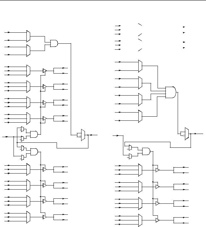
Data Sheet |
ORCA Series 3C and 3T FPGAs |
June 1999 |
Programmable Logic Cells (continued)
BRI9 |
|
|
|
BLI9 |
|
|
|
BRI8 |
|
|
|
BLI8 |
|
|
|
BRI7 |
|
BL07 |
|
I7 |
|
|
|
|
BR07 |
|
|
BLI7 |
|
|
|
|
|
|
|
BRI6 |
|
BL06 |
|
I6 |
|
|
|
|
BR06 |
|
|
BLI6 |
|
|
|
|
|
|
|
BRI5 |
|
BL05 |
|
I5 |
|
|
|
|
BR05 |
|
|
BLI5 |
|
|
|
|
|
|
|
BRI4 |
|
BL04 |
|
I4 |
|
|
|
|
BR04 |
|
|
BLI4 |
|
|
|
|
|
|
|
|
1 |
|
DEC |
TRI |
|
HIGH Z |
|
|
WHEN LOW |
|
|
|
|
|
|
|
1 |
|
|
|
1 |
HIGH Z |
|
|
|
|
|
|
|
WHEN LOW |
|
|
1 |
|
|
BRI3 |
|
BL03 |
|
I3 |
|
|
|
|
BR03 |
|
|
BLI3 |
|
|
|
|
|
|
|
BRI2 |
|
BL02 |
|
I2 |
|
|
|
|
BR02 |
|
|
BLI2 |
|
|
|
|
|
|
|
BRI1 |
|
BL01 |
|
I1 |
|
|
|
|
BR01 |
|
|
BLI1 |
|
|
|
|
|
|
|
BRI0 |
|
BL00 |
|
I0 |
|
|
|
|
BR00 |
|
|
BLI0 |
|
|
|
|
|
|
|
|
|
|
5-5746(F) |
Figure 13. Buffer-Buffer-Decoder Mode
BRI9 |
|
|
BL09 |
|
|
||
I9 |
|
|
BR09 |
BLI9 |
|
|
|
|
|
|
|
BRI8 |
|
|
BL08 |
|
|
||
|
|
||
I8 |
|
|
BR08 |
BLI8 |
|
|
|
|
|
|
|
|
|
|
|
BRI7
BLI7
BRI6
BLI6
BRI5
BLI5
BRI4
BLI4
DEC
TRI |
|
|
1 |
|
|
1 |
HIGH Z WHEN LOW |
|
|
||
BRI3 |
BL03 |
|
I3 |
||
BR03 |
||
BLI3 |
||
|
||
BRI2 |
BL02 |
|
I2 |
||
BR02 |
||
BLI2 |
||
|
||
BRI1 |
BL01 |
|
I1 |
||
BR01 |
||
BLI1 |
||
|
||
BRI0 |
BL00 |
|
I0 |
||
BR00 |
||
BLI0 |
||
|
5-5747(F)
Figure 14. Buffer-Decoder-Buffer Mode
Lucent Technologies Inc. |
23 |

ORCA Series 3C and 3T FPGAs |
Data Sheet |
June 1999 |
|
|
|
Programmable Logic Cells (continued)
BRI9 |
|
|
BLI9 |
|
|
BRI8 |
|
|
BLI8 |
|
|
BRI7 |
|
|
BLI7 |
|
|
BRI6 |
|
|
BLI6 |
|
|
BRI5 |
|
|
BLI5 |
|
|
BRI4 |
|
|
BLI4 |
|
|
|
DEC |
|
TRI |
|
|
1 |
|
|
|
HIGH Z WHEN LOW |
|
1 |
|
|
BRI3 |
BL03 |
|
I3 |
||
BR03 |
||
BLI3 |
||
|
||
BRI2 |
BL02 |
|
I2 |
||
BR02 |
||
BLI2 |
||
|
||
BRI1 |
BL01 |
|
I1 |
||
BR01 |
||
BLI1 |
||
|
||
BRI0 |
BL00 |
|
I0 |
||
BR00 |
||
BLI0 |
||
|
||
|
5-5750(F) |
Figure 15. Buffer-Decoder-Decoder Mode
BRI9
BLI9
BRI8
BLI8
BRI7
BLI7
BRI6
BLI6
BRI5
BLI5
BRI4
BLI4
DEC
BRI3 |
BLI3 |
BRI2
BLI2
BRI1
BLI1
BRI0
BLI0
5-5748(F)
Figure 16. Decoder Mode
24 |
Lucent Technologies Inc. |

Data Sheet |
ORCA Series 3C and 3T FPGAs |
June 1999 |
Programmable Logic Cells (continued)
PLC Latches/Flip-Flops
The eight general-purpose latches/FFs in the PFU can be used in a variety of configurations. In some cases, the configuration options apply to all eight latches/FFs in the PFU and some apply to the latches/FFs on a nibblewide basis where the ninth FF is considered independently. For other options, each latch/FF is independently programmable. In addition, the ninth FF can be used for a variety of functions.
Table 7 summarizes these latch/FF options. The latches/FFs can be configured as either positiveor negative-level sensitive latches, or positive or negative edge-triggered flip-flops (the ninth register can only be FF). All latches/FFs in a given PFU share the same clock, and the clock to these latches/FFs can be inverted. The input into each latch/FF is from either the corresponding LUT output (F[7:0]) or the direct data input (DIN[7:0]). The latch/FF input can also be tied to logic 1 or to logic 0, which is the default.
Table 7. Configuration RAM Controlled Latch/
Flip-Flop Operation
Function |
Options |
|
|
Common to All Latches/FFs in PFU |
|
|
|
LSR Operation |
Asynchronous or synchronous |
|
|
Clock Polarity |
Noninverted or inverted |
|
|
Front-end Select* |
Direct(DIN[7:0])orfromLUT(F[7:0]) |
|
|
LSR Priority |
Either LSR or CE has priority |
|
|
Latch/FF Mode |
Latch or flip-flop |
|
|
Enable GSRN |
GSRN enabled or has no effect on |
|
PFU latches/FFs |
|
|
Set Individually in Each Latch/FF in PFU |
|
|
|
Set/Reset Mode |
Set or reset |
|
|
By Group (Latch/FF[3:0], Latch/FF[7:4], and FF[8]) |
|
|
|
Clock Enable |
CE or ASWE or none |
|
|
LSR Control |
LSR or none |
|
|
* Not available for FF[8].
The eight latches/FFs in a PFU share the clock (CLK) and options for clock enable (CE), local set/reset (LSR), and front-end data select (SEL) inputs. When CE is disabled, each latch/FF retains its previous value when clocked. The clock enable, LSR, and SEL inputs can be inverted to be active-low.
The set/reset operation of the latch/FF is controlled by two parameters: reset mode and set/reset value. When the global set/reset (GSRN) and local set/reset (LSR) signals are not asserted, the latch/FF operates normally. The reset mode is used to select a synchronous or asynchronous LSR operation. If synchronous, LSR has the option to be enabled only if clock enable (CE or ASWE) is active or for LSR to have priority over the clock enable input, thereby setting/resetting the FF independent of the state of the clock enable. The clock enable is supported on FFs, not latches. It is implemented by using a 2-input multiplexer on the FF input, with one input being the previous state of the FF and the other input being the new data applied to the FF. The select of this 2-input multiplexer is clock enable (CE or ASWE), which selects either the new data or the previous state. When the clock enable is inactive, the FF output does not change when the clock edge arrives.
Lucent Technologies Inc. |
25 |

ORCA Series 3C and 3T FPGAs |
Data Sheet |
June 1999 |
|
|
|
Programmable Logic Cells (continued)
The GSRN signal is only asynchronous, and it sets/ resets all latches/FFs in the FPGA based upon the set/ reset configuration bit for each latch/FF. The set/reset value determines whether GSRN and LSR are set or reset inputs. The set/reset value is independent for each latch/FF. A new option is available to disable the GSRN function per PFU after initial device configuration.
The latch/FF can be configured to have a data frontend select. Two data inputs are possible in the frontend select mode, with the SEL signal used to select which data input is used. The data input into each latch/FF is from the output of its associated LUT, F[7:0], or direct from DIN[7:0], bypassing the LUT. In the frontend data select mode, both signals are available to the latches/FFs.
If either or both of these inputs is unused or is unavailable, the latch/FF data input can be tied to a logic 0 or logic 1 instead (the default is logic 0).
The latches/FFs can be configured in three basic modes:
1.Local synchronous set/reset: the input into the PFU’s LSR port is used to synchronously set or reset each latch/FF.
2.Local asynchronous set/reset: the input into LSR asynchronously sets or resets each latch/FF.
3.Latch/FF with front-end select, LSR either synchronous or asynchronous: the data select signal selects the input into the latches/FFs between the LUT output and direct data in.
For all three modes, each latch/FF can be independently programmed as either set or reset. Figure 17 provides the logic functionality of the front-end select, global set/reset, and local set/reset operations.
The ninth PFU FF, which is generally associated with registering the carry-out signal in ripple mode functions, can be used as a general-purpose FF. It is only an FF and is not capable of being configured as a latch. Because the ninth FF is not associated with an LUT, there is no front-end data select. The data input to the ninth FF is limited to the CIN input, logic 1, logic 0, or the carry-out in ripple and half-logic modes.
|
CE/ASWE |
|
|
CE/ASWE |
|
|
SEL |
CE/ASWE |
|
|
|
|
|
F |
|
|
|
||
|
|
|
|
|
|
|
|
|
|
F |
CE |
|
F |
CE |
|
DIN |
|
CE |
|
Q |
Q |
LOGIC 1 |
|
Q |
|||||
DIN |
D |
DIN |
D |
LOGIC 0 |
DIN |
D |
|||
LOGIC 1 |
|
|
LOGIC 1 |
|
|
|
|
||
|
|
|
|
|
|
|
|||
LOGIC 0 |
s_set |
|
LOGIC 0 |
|
|
|
|
|
|
|
|
|
|
|
|
|
|
|
|
LSR |
|
|
|
|
|
|
|
|
|
|
s_reset |
|
GSRN |
|
|
GSRN |
|
|
|
|
CLK |
|
CLK |
|
|
CLK |
|
||
|
|
LSR |
|
LSR |
|
|
|||
|
|
|
|
|
|
||||
|
SET RESET |
|
SET RESET |
|
|
SET RESET |
|||
GSRN |
|
|
|
|
|
|
|
|
|
|
CD |
|
|
CD |
|
|
CD |
|
|
Key: C = configuration data.
Figure 17. Latch/FF Set/Reset Configurations
26 |
Lucent Technologies Inc. |

Data Sheet |
ORCA Series 3C and 3T FPGAs |
June 1999 |
Programmable Logic Cells (continued)
PLC Routing Resources
Generally, the ORCA Foundry Development System is used to automatically route interconnections. Interactive routing with the ORCA Foundry design editor (EPIC) is also available for design optimization. To use EPIC for interactive layout, an understanding of the routing resources is needed and is provided in this section.
The routing resources consist of switching circuitry and metal interconnect segments. Generally, the metal lines which carry the signals are designated as routing segments. The switching circuitry connects the routing segments, providing one or more of three basic functions: signal switching, amplification, and isolation. A net running from a PFU or PIC output (source) to a PLC or PIC input (destination) consists of one or more routing segments, connected by switching circuitry called configurable interconnect points (CIPs).
The following sections discuss PLC, PIC, and interquad routing resources. This section discusses the PLC switching circuitry, intra-PLC routing, inter-PLC routing, and clock distribution.
Configurable Interconnect Points
The process of connecting routing segments uses three basic types of switching circuits: two types of configurable interconnect points (CIPs) and bidirectional buffers (BIDIs). The basic element in CIPs is one or more pass transistors, each controlled by a configuration RAM bit. The two types of CIPs are the mutually exclusive (or multiplexed) CIP and the independent CIP.
A mutually exclusive set of CIPs contains two or more CIPs, only one of which can be on at a time. An independent CIP has no such restrictions and can be on independent of the state of other CIPs. Figure 18 shows an example of both types of CIPs.
|
|
|
|
|
|
|
INDEPENDENT CIP |
|
|
|
|
|
|
|
|
||||
|
|
|
|
B |
|
|
|
|
|
|
|
|
|||||||
|
|
|
|
|
|
|
= |
|
|
|
|
CD |
|
||||||
|
A |
|
|
|
|
A |
|
|
|
|
|
|
|
|
|
|
B |
||
|
|
|
|
|
|
|
|
|
|
|
|
|
|
|
|
|
|
||
|
|
|
|
|
|
|
|
|
|
|
|
|
|
|
|
|
|
||
|
|
|
|
|
|
|
|
|
|
|
|
|
|
|
|
|
|||
|
|
|
|
|
|
|
MULTIPLEXED CIP |
|
|
|
|
|
|
|
|
||||
|
|
|
|
|
|
|
|
|
|
|
|
|
|
|
|
|
|
||
|
|
O |
|
|
CD |
|
|||||||||||||
A |
|
|
|
|
|
2 |
|
|
|
||||||||||
|
|
|
|
|
|
|
|
A |
|
|
|
|
|
|
|
|
|||
|
|
|
|
|
|
|
|
|
|
||||||||||
|
|
|
|
|
|
|
|
|
|
|
|
|
|
|
|
|
|
||
B |
|
|
|
|
|
|
|
|
|
|
|
|
|
|
|
|
|
|
|
|
|
|
|
|
|
|
|
B |
|
|
|
|
|
|
|
|
|
O |
|
|
|
|
|
|
|
|
|
|
|
|
|
|
|
|
|
||||
C |
|
|
|
|
|
|
|
|
C |
|
|
|
|
|
|
|
|
|
|
|
|
|
|
|
|
|
|
|
|
|
|
|
|
|
|||||
|
|
|
|
|
|
|
|
|
|
|
|
|
|
|
|
|
|||
|
|
|
|
|
|
|
|
|
|
|
|
|
|
|
|
|
|
|
|
|
|
|
|
|
|
|
|
|
|
|
|
|
|
|
|
|
|
|
|
|
|
|
|
|
|
|
|
|
|
|
|
|
|
|
|
|
|
|
|
Key: C = configuration data.
5-5973(C)
Figure 18. Configurable Interconnect Point
3-Statable Bidirectional Buffers
Bidirectional buffers, previously described in the SLIC section of the programmable logic cell discussion, provide isolation as well as amplification for signals routed a long distance. Bidirectional buffers are also used to route signals diagonally in the PLC (described later in the subsection entitled Intra-PLC Routing), and BIDIs can be used to indirectly route signals through the switching routing (xSW) segments. Any number from zero to ten BIDIs can be used in a given PLC.
Lucent Technologies Inc. |
27 |

ORCA Series 3C and 3T FPGAs |
Data Sheet |
June 1999 |
|
|
|
Programmable Logic Cells (continued)
General Routing Structure
Routing resources in Series 3 FPGAs generally consist of routing segments in groups of ten, with varying lengths and connectivity to logic and other routing resources. The varying lengths of routing segments provides a hierarchy of routing capability from chip-length routes to routes within a PLC. The hierarchical nature of the routing provides the ORCA Foundry development tools with the necessary resources to route a design completely and to optimize the routing for system speed while reducing the overall power required by the device.
Within each group of ten routing segments there is an equivalency of connectivity between pairs of segments. These pairs are segments: [0, 4] and [1, 5] and [2, 6] and [3, 7] and [8, 9]. The equivalency in connectivity ensures that signals on either segment in a pair have the same capability to get to a given destination. This, in turn, allows for signal distribution from a source to varying destinations without using special routing. It also provides for routing flexibility by ensuring that one segment position will not become so congested as to preclude routing a bus or group of signals and allows easy connectivity from either of the twin quads in a source PFU to either of the twin quads in any destination PFU.
Having ten segments in a group is significant in that it provides for routing a byte of data and two control signals or parity. Due to the equivalent pairs of segments, this can also be viewed as routing two nibbles each with a control signal. Figure 19 is an overview of the routing for a single PLC.
BL[9:0] |
vxL[9:0] |
vx5[9:0] |
vx1L[9:0] |
SUL[9:0] |
vx1R[9:0] |
FC |
LCK |
VCK |
vxH[9:0] |
BL[9:0] |
|
|
|
|
|
|
|
|
|
|
hxH[9:0] |
|
|
|
|
|
|
|
|
|
|
hx1U[9:0] |
|
|
|
|
|
|
|
|
|
|
hCK |
FC |
|
|
|
|
|
|
|
|
|
FC |
|
|
|
|
|
|
|
|
|
|
SLL[9:0] |
SLL[9:0] |
|
|
|
|
|
|
|
|
|
|
|
|
|
|
|
|
FINS |
PFU |
|
|
|
|
|
|
5 |
|
|
|
|
|
|
|
|
|
2 |
|
SLR[9:0] |
|
|
|
|
|
|
|
|
|
|
|
|
|
|
|
|
|
|
|
|
|
SLIC |
|
|
|
|
|
|
|
|
|
|
|
|
|
OUTPUT |
|
|
|
|
|
|
|
|
|
|
SWITCHING |
|
|
|
|
|
|
|
|
|
|
SUR[9:0] |
|
|
|
LCK |
|
|
|
|
|
|
|
|
|
|
|
|
|
|
|
|
|
|
|
|
hx1B[9:0] |
|
|
|
|
|
|
|
2 |
|
|
hx5[9:0] |
|
|
|
|
|
|
|
5 |
|
|
|
|
|
|
|
|
|
|
|
|
|
|
|
|
|
|
|
|
|
|
|
|
hxL[9:0] |
BR[9:0] |
|
|
|
|
|
|
|
|
|
BR[9:0] |
|
|
|
|
|
|
|
|
|
|
SUL[9:0] |
|
|
|
|
SUL[9:0] |
|
|
|
FC |
|
BL[9:0] |
KEY: CONFIGURABLE SIGNAL LINE BREAKS
LINE-BY-LINE
2

 2 OF 5 5
5-5766(F)
Figure 19. Single PLC View of Inter-PLC Route Segments
28 |
Lucent Technologies Inc. |

Data Sheet |
ORCA Series 3C and 3T FPGAs |
June 1999 |
Programmable Logic Cells (continued)
Intra-PLC Routing
The function of the intra-PLC routing resources is to connect the PFU’s input and output ports to the routing resources used for entry to and exit from the PLC. This routing provides PFU feedback, corner turning, or switching from one type of routing resource to another.
Flexible Input Structure (FINS)
The flexible input switching structure (FINS) in each PLC of the ORCA Series 3 provides for the flexibility of a crossbar switch from the routing resources to the PFU inputs while taking advantage of the routability of shared inputs. Connectivity between the PLC routing resources and the PFU inputs is provided in two stages. The primary FINS switch has 50 inputs that connect the PLC routing to the 35 inputs on the secondary switch. The outputs of the second switch connect to the 50 PFU inputs. The switches are implemented to provide connectivity for bused signals and individual connections.
PFU Output Switching
The PFU outputs are switched onto PLC routing resources via the PFU output multiplexer (OMUX). The PFU output switching segments from the output multiplexer provide ten connections to the PLC routing out of 18 possible PFU outputs (F[7:0], Q[7:0], DOUT, REGCOUT). These output switching segments connect segment for segment to the SUR, SUL, SLR, and SLL switching segments described below (e.g., O4 connects only to SUR4, not SUR5). The output switching segments also feed directly into the SLIC on a seg- ment-by-segment basis. This connectivity is also described below.
Switching Routing Segments (xSW)
There are four sets of switching routing segments in each PLC. Each set consists of ten switching elements: SUL[9:0], SUR[9:0], SLL[9:0], and SLR[9:0], tradition-
ally labeled for the upper-left, upper-right, lower-left, and lower-right sections of the PFUs, respectively. The xSW routing segments connect to the PFU inputs and outputs as well as the BIDI routing segments, to be described later. They also connect to both the horizontal and vertical x1 and x5 routing segments (inter-PLC routing resources, described later) in their specific corner. xSW segments can be used for fast connections between adjacent PLCs or PICs without requiring the use of inter-PLC routing resources. This capability not only increases signal speed on adjacent PLC routing, but also reduces routing congestion on the principal inter-PLC routing resources. The SLL and SUR segments combine to provide connectivity to the PLCs to the left and right of the current PLC; the SLR and SUL segments combine to provide connectivity to the PLCs above and below the current PLC.
Fast routes on switching segments to diagonally adjacent PLCs/PICs are possible using the BIDI routing segments (discussed below) and the SLL and SLR switching segments. The BR BIDI routing segments combine with the SUL switching segments of the PLC below and to the right of the current PLC to connect to that PLC. The BL BIDI routing segments combine with the SLL switching segments of the PLC above and to the right of the current PLC to connect to that PLC. These fast diagonal connections provide a great amount of flexibility in routing congested areas of logic and in shifting data on a per-PLC basis such as performing implicit multiplications/divisions in routing between functional logic elements.
Switching routing segments are also the chief means by which signals are transferred between the inter-PLC routing resources and the PFU. Each set of switching segments has connectivity to the x1 routing segments, and there is varying connectivity to the x5, xH, and xL inter-PLC routing segments. Detailed information on switching segment/inter-PLC routing connectivity is provided later in this section in the Inter-PLC Routing Resources subsection.
Lucent Technologies Inc. |
29 |
ORCA Series 3C and 3T FPGAs |
Data Sheet |
June 1999 |
|
|
|
Programmable Logic Cells (continued)
BIDI Routing and SLIC Connectivity
The SLIC is connected to the rest of the PLC by the bidirectional (BIDI) routing segments and the PFU output switching segments coming from the PFU output multiplexer. The BIDI routing segments (xBID) are labeled as BL for BIDI-left and BR for BIDI-right. Each set of BR and BL xBID segments is composed of ten bidirectional lines (note that these lines are diagramed as ten input lines to the SLIC and ten output lines from the SLIC that can be used in a mutually exclusive fashion). Because the SLIC is connected directly to the outputs of the PFU, it provides great flexibility in routing via the xBID segments. The PFU routing segments, O[9:0], only connect to their respective line in the SLL, SUL, SUR, and SLR switching segment groups. That is, O9 only connects to SLL9, SUL9, SUR9, and SLR9. The BIDI lines provide the capability to connect to the other member of the routing set. That means, for example, that O9 can be routed to BR8 or BL8. This connectivity can be used as a means to distribute or gather signals on intra-PLC routing without disturbing inter-PLC resources. As described in the Switching Routing Segments subsection, the BIDI routing segments are also used for routes to a diagonally adjacent PFU.
In addition to the intra-PLC connections, the xBID and output switching segments also have connectivity to the x1, x5, and xL inter-PLC routing resources, providing an alternate routing path rather than using PLC xSW segments. These connections also provide a path to the 3-state buffers in the SLIC without encumbering the xSW segments. In this manner, buffering or 3-state control can be added to inter-PLC routing without disturbing local functionality within a PFU.
Control Signal and Fast-Carry Routing
PFU control signal and the fast-carry routing are performed using the FINS structure and several dedicated routing paths. The fast-carry (FC) routing resources consist of a dedicated bidirectional segment between each orthogonal pair of PLCs. This means that a fastcarry can go to or come from each PLC to the right or left, above or below the subject PLC. The FINS structure is used to control the switching of these fast-carry paths between the fast-carry input (FCIN) and fastcarry output (FCOUT) ports of the PFU.
The PFU control inputs (CE, SEL, LSR, ASWE) and CIN can be reached via the FINS by two special routing segments, E1 and E2. The E1 routing segment provides connectivity between all of the xBID routing segments and the FINS. It is unidirectional from the BIDI routing to the FINS. E1 also provides connectivity to the PFU clock input via FINS for a local clock signal. The E2 segment connects the SLIC DEC output to the FINS and to a group of CIPS that provide bidirectional connectivity with all of the BIDI routing segments. This allows the DEC signal to be used in the PFU and/or routed on the BIDI segments. It also allows signals to be routed to the PFU on the xBID segments if the SLIC DEC output is not used.
There is also a dedicated routing segment from the FINS to the SLIC TRI input used for BIDI buffer 3-state control.
30 |
Lucent Technologies Inc. |
 Loading...