


AGERE OR2C04A-4T100I, OR2C06A-4J160I, OR2C06A-4M84, OR2C04A-4J160, OR2C04A-4J160I Datasheet
...Data Sheet
June 1999
ORCA® Series 2
Field-Programmable Gate Arrays
Features
■High-performance, cost-effective, low-power
0.35 µm CMOS technology (OR2CxxA), 0.3 µm CMOS technology (OR2TxxA), and 0.25 µm CMOS technology (OR2TxxB), (four-input look-up table (LUT) delay less than 1.0 ns with -8 speed grade)
■High density (up to 43,200 usable, logic-only gates; or 99,400 gates including RAM)
■Up to 480 user I/Os (OR2TxxA and OR2TxxB I/Os are 5 V tolerant to allow interconnection to both 3.3 V and 5 V devices, selectable on a per-pin basis)
■Four 16-bit look-up tables and four latches/flip-flops per PFU, nibble-oriented for implementing 4-, 8-, 16-, and/or 32-bit (or wider) bus structures
■Eight 3-state buffers per PFU for on-chip bus structures
■Fast, on-chip user SRAM has features to simplify RAM design and increase RAM speed:
— Asynchronous single port: 64 bits/PFU
— Synchronous single port: 64 bits/PFU
— Synchronous dual port: 32 bits/PFU
■Improved ability to combine PFUs to create larger RAM structures using write-port enable and 3-state buffers
■Fast, dense multipliers can be created with the multiplier mode (4 x 1 multiplier/PFU):
— 8 x 8 multiplier requires only 16 PFUs
— 30% increase in speed
■Flip-flop/latch options to allow programmable priority of synchronous set/reset vs. clock enable
■Enhanced cascadable nibble-wide data path capabilities for adders, subtractors, counters, multipliers, and comparators including internal fast-carry operation
Table 1. ORCA Series 2 FPGAs
■Innovative, abundant, and hierarchical nibbleoriented routing resources that allow automatic use of
internal gates for all device densities without sacrificing performance
■Upward bit stream compatible with the ORCA ATT2Cxx/ ATT2Txx series of devices
■Pinout-compatible with new ORCA Series 3 FPGAs
■TTL or CMOS input levels programmable per pin for the OR2CxxA (5 V) devices
■Individually programmable drive capability:
12 mA sink/6 mA source or 6 mA sink/3 mA source
■Built-in boundary scan (IEEE*1149.1 JTAG) and 3-state all I/O pins, (TS_ALL) testability functions
■Multiple configuration options, including simple, low pincount serial ROMs, and peripheral or JTAG modes for insystem programming (ISP)
■Full PCI bus compliance for all devices
■Supported by industry-standard CAE tools for design entry, synthesis, and simulation with ORCA Foundry Development System support (for back-end implementation)
■New, added features (OR2TxxB) have:
—More I/O per package than the OR2TxxA family
—No dedicated 5 V supply (V DD5)
—Faster configuration speed (40 MHz)
—Pin selectable I/O clamping diodes provide 5V or 3.3V PCI compliance and 5V tolerance
—Full PCI bus compliance in both 5V and 3.3V PCI systems
*IEEE is a registered trademark of The Institute of Electrical and Electronics Engineers, Inc.
Device |
Usable |
# LUTs |
Registers |
Max User |
User |
Array Size |
|
Gates* |
RAM Bits |
I/Os |
|||||
|
|
|
|
||||
|
|
|
|
|
|
|
|
OR2C04A/OR2T04A |
4,800—11,000 |
400 |
400 |
6,400 |
160 |
10 x 10 |
|
|
|
|
|
|
|
|
|
OR2C06A/OR2T06A |
6,900—15,900 |
576 |
576 |
9,216 |
192 |
12 x 12 |
|
|
|
|
|
|
|
|
|
OR2C08A/OR2T08A |
9,400—21,600 |
784 |
724 |
12,544 |
224 |
14 x 14 |
|
|
|
|
|
|
|
|
|
OR2C10A/OR2T10A |
12,300—28,300 |
1024 |
1024 |
16,384 |
256 |
16 x 16 |
|
|
|
|
|
|
|
|
|
OR2C12A/OR2T12A |
15,600—35,800 |
1296 |
1296 |
20,736 |
288 |
18 x 18 |
|
|
|
|
|
|
|
|
|
OR2C15A/OR2T15A/OR2T15B |
19,200—44,200 |
1600 |
1600 |
25,600 |
320 |
20 x 20 |
|
|
|
|
|
|
|
|
|
OR2C26A/OR2T26A |
27,600—63,600 |
2304 |
2304 |
36,864 |
384 |
24 x 24 |
|
|
|
|
|
|
|
|
|
OR2C40A/OR2T40A/OR2T40B |
43,200—99,400 |
3600 |
3600 |
57,600 |
480 |
30 x 30 |
|
|
|
|
|
|
|
|
*The first number in the usable gates column assumes 48 gates per PFU (12 gates per four-input LUT/FF pair) for logic-only designs. The second number assumes 30% of a design is RAM. PFUs used as RAM are counted at four gates per bit, with each PFU capable of implementing a 16 x 4 RAM (or 256 gates) per PFU.
|
Data Sheet |
ORCA Series 2 FPGAs |
June 1999 |
|
|
Table of Contents
Contents |
Page |
Features ...................................................................... |
1 |
Description................................................................... |
3 |
ORCA Foundry Development System Overview......... |
5 |
Architecture ................................................................. |
5 |
Programmable Logic Cells .......................................... |
5 |
Programmable Function Unit ................................... |
5 |
Look-Up Table Operating Modes ............................ |
7 |
Latches/Flip-Flops ................................................. |
15 |
PLC Routing Resources ........................................ |
17 |
PLC Architectural Description................................ |
22 |
Programmable Input/Output Cells ............................. |
25 |
Inputs..................................................................... |
25 |
Outputs .................................................................. |
26 |
5 V Tolerant I/O (OR2TxxB) .................................. |
27 |
PCI Compliant I/O.................................................. |
27 |
PIC Routing Resources ......................................... |
28 |
PIC Architectural Description................................. |
29 |
PLC-PIC Routing Resources ................................. |
30 |
Interquad Routing ...................................................... |
32 |
Subquad Routing (OR2C40A/OR2T40A Only)...... |
34 |
PIC Interquad (MID) Routing ................................. |
36 |
Programmable Corner Cells ...................................... |
37 |
Programmable Routing.......................................... |
37 |
Special-Purpose Functions.................................... |
37 |
Clock Distribution Network ........................................ |
37 |
Primary Clock ........................................................ |
37 |
Secondary Clock ................................................... |
38 |
Selecting Clock Input Pins..................................... |
39 |
FPGA States of Operation......................................... |
40 |
Initialization............................................................ |
40 |
Configuration ......................................................... |
41 |
Start-Up ................................................................. |
42 |
Reconfiguration ..................................................... |
42 |
Partial Reconfiguration .......................................... |
43 |
Other Configuration Options.................................. |
43 |
Configuration Data Format ........................................ |
43 |
Using ORCA Foundry to Generate |
|
Configuration RAM Data..................................... |
44 |
Configuration Data Frame ..................................... |
44 |
Bit Stream Error Checking......................................... |
47 |
FPGA Configuration Modes....................................... |
47 |
Master Parallel Mode............................................. |
47 |
Master Serial Mode ............................................... |
48 |
Asynchronous Peripheral Mode ............................ |
49 |
Synchronous Peripheral Mode .............................. |
49 |
Slave Serial Mode ................................................. |
50 |
Slave Parallel Mode............................................... |
50 |
Daisy Chain ........................................................... |
51 |
Special Function Blocks ............................................ |
52 |
Single Function Blocks .......................................... |
52 |
Boundary Scan ...................................................... |
54 |
Contents |
Page |
Boundary-Scan Instructions................................... |
55 |
ORCA Boundary-Scan Circuitry ............................ |
56 |
ORCA Timing Characteristics.................................... |
60 |
Estimating Power Dissipation .................................... |
61 |
OR2CxxA............................................................... |
61 |
OR2TxxA ............................................................... |
63 |
OR2T15B and OR2T40B....................................... |
65 |
Pin Information .......................................................... |
66 |
Pin Descriptions..................................................... |
66 |
Package Compatibility ........................................... |
68 |
Compatibility with Series 3 FPGAs ........................ |
70 |
Package Thermal Characteristics............................ |
126 |
QJA...................................................................... |
126 |
yJC....................................................................... |
126 |
QJC...................................................................... |
126 |
QJB...................................................................... |
126 |
Package Coplanarity ............................................... |
127 |
Package Parasitics .................................................. |
127 |
Absolute Maximum Ratings ..................................... |
129 |
Recommended Operating Conditions...................... |
129 |
Electrical Characteristics ......................................... |
130 |
Timing Characteristics ............................................. |
132 |
Series 2................................................................ |
160 |
Measurement Conditions......................................... |
169 |
Output Buffer Characteristics................................... |
170 |
OR2CxxA............................................................. |
170 |
OR2TxxA ............................................................. |
171 |
OR2TxxB ............................................................. |
172 |
Package Outline Drawings ...................................... |
173 |
Terms and Definitions.......................................... |
173 |
84-Pin PLCC........................................................ |
174 |
100-Pin TQFP...................................................... |
175 |
144-Pin TQFP...................................................... |
176 |
160-Pin QFP ........................................................ |
177 |
208-Pin SQFP...................................................... |
178 |
208-Pin SQFP2.................................................... |
179 |
240-Pin SQFP...................................................... |
180 |
240-Pin SQFP2.................................................... |
181 |
256-Pin PBGA ..................................................... |
182 |
304-Pin SQFP...................................................... |
183 |
304-Pin SQFP2.................................................... |
184 |
352-Pin PBGA ..................................................... |
185 |
432-Pin EBGA ..................................................... |
186 |
Ordering Information................................................ |
187 |
Index ........................................................................ |
189 |
2 |
Lucent Technologies Inc. |

Data Sheet |
|
June 1999 |
ORCA Series 2 FPGAs |
Description
The ORCA Series 2 series of SRAM-based FPGAs are an enhanced version of the ATT2C/2T architecture. The latest ORCA series includes patented architectural enhancements that make functions faster and easier to design while conserving the use of PLCs and routing resources.
The Series 2 devices can be used as drop-in replacements for the ATT2Cxx/ATT2Txx series, respectively, and they are also bit stream compatible with each other. The usable gate counts associated with each series are provided in Table 1. Both series are offered in a variety of packages, speed grades, and temperature ranges.
The ORCA series FPGA consists of two basic elements: programmable logic cells (PLCs) and program-
Table 2. ORCA Series 2 System Performance
mable input/output cells (PICs). An array of PLCs is surrounded by PICs as shown in Figure 1. Each PLC contains a programmable function unit (PFU). The PLCs and PICs also contain routing resources and configuration RAM. All logic is done in the PFU. Each PFU contains four 16-bit look-up tables (LUTs) and four latches/flip-flops (FFs).
The PLC architecture provides a balanced mix of logic and routing that allows a higher utilized gate/PFU than alternative architectures. The routing resources carry logic signals between PFUs and I/O pads. The routing in the PLC is symmetrical about the horizontal and vertical axes. This improves routability by allowing a bus of signals to be routed into the PLC from any direction.
Some examples of the resources required and the performance that can be achieved using these devices are represented in Table 2.
Function |
# |
|
|
|
Speed Grade |
|
|
|
Unit |
||
|
|
|
|
|
|
|
|
||||
PFUs |
-2A |
-3A |
-4A |
-5A |
-6A |
-7A |
-7B |
-8B |
|||
|
|
||||||||||
|
|
|
|||||||||
|
|
|
|
|
|
|
|
|
|
|
|
16-bit loadable up/down |
4 |
51.0 |
66.7 |
87.0 |
104.2 |
129.9 |
144.9 |
131.6 |
149.3 |
MHz |
|
counter |
|
|
|
|
|
|
|
|
|
|
|
|
|
|
|
|
|
|
|
|
|
|
|
16-bit accumulator |
4 |
51.0 |
66.7 |
87.0 |
104.2 |
129.9 |
144.9 |
131.6 |
149.3 |
MHz |
|
|
|
|
|
|
|
|
|
|
|
|
|
8 x 8 parallel multiplier: |
|
|
|
|
|
|
|
|
|
|
|
— Multiplier mode, unpipelined 1 |
22 |
14.2 |
19.3 |
25.1 |
31.0 |
36.0 |
40.3 |
37.7 |
44.8 |
MHz |
|
— ROM mode, unpipelined 2 |
9 |
41.5 |
55.6 |
71.9 |
87.7 |
107.5 |
122.0 |
103.1 |
120.5 |
MHz |
|
— Multiplier mode, pipelined 3 |
44 |
50.5 |
69.0 |
82.0 |
103.1 |
125.0 |
142.9 |
123.5 |
142.9 |
MHz |
|
32 x 16 RAM: |
|
|
|
|
|
|
|
|
|
|
|
— Single port (read and write/ |
9 |
21.8 |
28.6 |
36.2 |
53.8 |
53.8 |
62.5 |
57.5 |
69.4 |
MHz |
|
cycle)4 |
|
|
|
|
|
|
|
|
|
|
|
— Single port 5 |
9 |
38.2 |
52.6 |
69.0 |
92.6 |
92.6 |
96.2 |
97.7 |
112.4 |
MHz |
|
— Dual port 6 |
16 |
38.2 |
52.6 |
83.3 |
92.6 |
92.6 |
96.2 |
97.7 |
112.4 |
MHz |
|
36-bit parity check (internal) |
4 |
13.9 |
11.0 |
9.1 |
7.4 |
5.6 |
5.2 |
6.1 |
5.1 |
ns |
|
|
|
|
|
|
|
|
|
|
|
|
|
32-bit address decode |
3.25 |
12.3 |
9.5 |
7.5 |
6.1 |
4.6 |
4.3 |
4.8 |
4.0 |
ns |
|
(internal) |
|
|
|
|
|
|
|
|
|
|
|
|
|
|
|
|
|
|
|
|
|
|
|
1.Implemented using 4 x 1 multiplier mode (unpipelined), register-to-register, two 8-bit inputs, one 16-bit output.
2.Implemented using two 16 x 12 ROMs and one 12-bit adder, one 8-bit input, one fixed operand, one 16-bit output.
3.Implemented using 4 x 1 multiplier mode (fully pipelined), two 8-bit inputs, one 16-bit output (28 of 44 PFUs contain only pipelining registers).
4.Implemented using 16 x 4 synchronous single-port RAM mode allowing both read and write per clock cycle, including write/read address multiplexer.
5.Implemented using 16 x 4 synchronous single-port RAM mode allowing either read or write per clock cycle, including write/read address multiplexer.
6.Implemented using 16 x 2 synchronous dual-port RAM mode.
7.OR2TxxB available only in -7 and -8 speeds only.
8.Speed grades of -5, -6, and -7 are for OR2TxxA devices only.
Lucent Technologies Inc. |
3 |

|
Data Sheet |
ORCA Series 2 FPGAs |
June 1999 |
|
|
Description (continued)
The FPGA’s functionality is determined by internal configuration RAM. The FPGA’s internal initialization/configuration circuitry loads the configuration data at powerup or under system control. The RAM is loaded by using one of several configuration modes. The configuration data resides externally in an EEPROM, EPROM, or ROM on the circuit board, or any other storage media. Serial ROMs provide a simple, low pin count method for configuring FPGAs, while the peripheral and JTAG configuration modes allow for easy, in-system programming (ISP).
PL18 PL17 PL16 PL15 PL14 PL13 PL12 PL11 PL10 LMID PL9 PL8 PL7 PL6 PL5 PL4 PL3 PL2 PL1
|
|
|
|
|
|
|
|
|
|
|
|
|
|
|
|
|
|
|
|
|
|
|
|
|
|
|
|
|
|
|
|
|
|
|
|
|
|
|
|
|
|
|
|
|
|
|
|
|
|
|
|
|
|
|
PT1 |
PT2 |
PT3 |
PT4 |
PT5 |
PT6 |
PT7 |
PT8 |
PT9 |
TMID |
|
PT10 |
|
PT11 |
|
PT12 |
PT13 |
PT14 |
PT15 |
PT16 |
PT17 |
PT18 |
|
|
|
|
|
R1C1 |
R1C2 |
R1C3 |
R1C4 |
R1C5 |
R1C6 |
R1C7 |
R1C8 |
R1C9 |
|
R1C10 |
|
R1C11 |
R1C12 |
R1C13 |
R1C14 |
R1C15 |
R1C16 |
R1C17 |
R1C18 |
|
PR1 |
|
|
||
|
|
|
|
|
|
|
|
|
|
|
|
|
|
|
|
|
|
|
|
|
|
|
|
|
|
|
|
R2C1 |
R2C2 |
R2C3 |
R2C4 |
R2C5 |
R2C6 |
R2C7 |
R2C8 |
R2C9 |
vIQ |
R2C10 |
|
R2C11 |
R2C12 |
R2C13 |
R2C14 |
R2C15 |
R2C16 |
R2C17 |
R2C18 |
|
PR2 |
|
|
||
|
|
|
|
|
|
|
||||||||||||||||||||
|
|
|
|
|
|
|
|
|
|
|
|
|
|
|
|
|
|
|
|
|
|
|
|
|
|
|
|
R3C1 |
R3C2 |
R3C3 |
R3C4 |
R3C5 |
R3C6 |
R3C7 |
R3C8 |
R3C9 |
|
R3C10 |
|
R3C11 |
R3C12 |
R3C13 |
R3C14 |
R3C15 |
R13C16 |
R3C17 |
R3C18 |
|
PR3 |
|
|
||
|
|
|
|
|
|
|
|
|
|
|
|
|
|
|
|
|
|
|
|
|
|
|
|
|
|
|
|
R4C1 |
R4C2 |
R4C3 |
R4C4 |
R4C5 |
R4C6 |
R4C7 |
R4C8 |
R4C9 |
|
R4C10 |
|
R4C11 |
R4C12 |
R4C13 |
R4C14 |
R4C15 |
R4C16 |
R4C17 |
R4C18 |
|
PR4 |
|
|
||
|
|
|
|
|
|
|
||||||||||||||||||||
|
|
|
|
|
|
|
|
|
|
|
|
|
|
|
|
|
|
|
|
|
|
|
|
|
|
|
|
R5C1 |
R5C2 |
R5C3 |
R5C4 |
R5C5 |
R5C6 |
R5C7 |
R5C8 |
R5C9 |
|
R5C10 |
|
R5C11 |
R5C12 |
R5C13 |
R5C14 |
R5C15 |
R5C16 |
R5C17 |
R5C18 |
|
PR5 |
|
|
||
|
|
|
|
|
|
|
||||||||||||||||||||
|
|
|
|
|
|
|
|
|
|
|
|
|
|
|
|
|
|
|
|
|
|
|
|
|
|
|
|
R6C1 |
R6C2 |
R6C3 |
R6C4 |
R6C5 |
R6C6 |
R6C7 |
R6C8 |
R6C9 |
|
R6C10 |
|
R6C11 |
R6C12 |
R6C13 |
R6C14 |
R6C15 |
R6C16 |
R6C17 |
R6C18 |
|
PR6 |
|
|
||
|
|
|
|
|
|
|
|
|
|
|
|
|
|
|
|
|
|
|
|
|
|
|
|
|
|
|
|
R7C1 |
R7C2 |
R7C3 |
R7C4 |
R7C5 |
R7C6 |
R7C7 |
R7C8 |
R7C9 |
|
R7C10 |
|
R7C11 |
R7C12 |
R7C13 |
R7C14 |
R7C15 |
R7C16 |
R7C17 |
R7C18 |
|
PR7 |
|
|
||
|
|
|
|
|
|
|
||||||||||||||||||||
|
|
|
|
|
|
|
|
|
|
|
|
|
|
|
|
|
|
|
|
|
|
|
|
|
|
|
|
R8C1 |
R8C2 |
R8C3 |
R8C4 |
R8C5 |
R8C6 |
R8C7 |
R8C8 |
R8C9 |
|
R8C10 |
|
R8C11 |
R8C12 |
R8C13 |
R8C14 |
R8C15 |
R8C16 |
R8C17 |
R8C18 |
|
PR8 |
|
|
||
|
|
|
|
|
|
|
||||||||||||||||||||
|
|
|
|
|
|
|
|
|
|
|
|
|
|
|
|
|
|
|
|
|
|
|
|
|
|
|
|
R9C1 |
R9C2 |
R9C3 |
R9C4 |
R9C5 |
R9C6 |
R9C7 |
R9C8 |
R9C9 |
|
R9C10 |
|
R9C11 |
R9C12 |
R9C13 |
R9C14 |
R9C15 |
R9C16 |
R9C17 |
R9C18 |
|
PR9 |
|
|
||
|
|
|
|
|
|
|
|
|
|
|
|
|
|
|
|
|
|
|
|
|
|
|
|
|
|
|
|
|
hIQ |
|
|
|
|
|
|
|
|
|
|
|
|
|
|
|
|
|
|
|
|
|
PR10 |
|
|
|
|
|
|
|
|
|
|
|
|
|
|
|
|
|
|
|
|
|
|
|
|
|
|
|
|
|
|
R10C1 |
R10C2 |
R10C3 |
R10C4 |
R10C5 |
R10C6 |
R10C7 |
R10C8 |
R10C9 |
|
R10C10 |
R10C11 |
R10C12 |
R10C13 |
R10C14 |
R10C15 |
R10C16 |
R10C17 |
R10C18 |
|
RMID |
|
|
|||
|
|
|
|
|
|
|||||||||||||||||||||
|
|
|
|
|
|
|
|
|
|
|
|
|
|
|
|
|
|
|
|
|
|
|
|
|
|
|
|
R11C1 |
R11C2 |
R11C3 |
R11C4 |
R11C5 |
R11C6 |
R11C7 |
R11C8 |
R11C9 |
|
R11C10 |
R11C11 |
R11C12 |
R11C13 |
R11C14 |
R11C15 |
R11C16 |
R11C17 |
R11C18 |
|
PR11 |
|
|
|||
|
|
|
|
|
|
|||||||||||||||||||||
|
|
|
|
|
|
|
|
|
|
|
|
|
|
|
|
|
|
|
|
|
|
|
|
|
|
|
|
R12C1 |
R12C2 |
R12C3 |
R12C4 |
R12C5 |
R12C6 |
R12C7 |
R12C8 |
R12C9 |
|
R12C10 |
R12C11 |
R12C12 |
R12C13 |
R12C14 |
R12C15 |
R12C16 |
R12C17 |
R12C18 |
|
PR12 |
|
|
|||
|
|
|
|
|
|
|||||||||||||||||||||
|
|
|
|
|
|
|
|
|
|
|
|
|
|
|
|
|
|
|
|
|
|
|
|
|
|
|
|
R13C1 |
R13C2 |
R13C3 |
R13C4 |
R13C5 |
R13C6 |
R13C7 |
R13C8 |
R13C9 |
|
R13C10 |
R13C11 |
R13C12 |
R13C13 |
R13C14 |
R13C15 |
R13C16 |
R13C17 |
R13C18 |
|
PR13 |
|
|
|||
|
|
|
|
|
|
|
|
|
|
|
|
|
|
|
|
|
|
|
|
|
|
|
|
|
|
|
|
R14C1 |
R14C2 |
R14C3 |
R14C4 |
R14C5 |
R14C6 |
R14C7 |
R14C8 |
R14C9 |
|
R14C10 |
R14C11 |
R14C12 |
R14C13 |
R14C14 |
R14C15 |
R14C16 |
R14C17 |
R14C18 |
|
PR14 |
|
|
|||
|
|
|
|
|
|
|||||||||||||||||||||
|
|
|
|
|
|
|
|
|
|
|
|
|
|
|
|
|
|
|
|
|
|
|
|
|
|
|
|
R15C1 |
R15C2 |
R15C3 |
R15C4 |
R15C5 |
R15C6 |
R15C7 |
R15C8 |
R15C9 |
|
R15C10 |
R15C11 |
R15C12 |
R15C13 |
R15C14 |
R15C15 |
R15C16 |
R15C17 |
R15C18 |
|
PR15 |
|
|
|||
|
|
|
|
|
|
|||||||||||||||||||||
|
|
|
|
|
|
|
|
|
|
|
|
|
|
|
|
|
|
|
|
|
|
|
|
|
|
|
|
R16C1 |
R16C2 |
R16C3 |
R16C4 |
R16C5 |
R16C6 |
R16C7 |
R16C8 |
R16C9 |
|
R16C10 |
R16C11 |
R16C12 |
R16C13 |
R16C14 |
R16C15 |
R16C16 |
R16C17 |
R16C18 |
|
PR16 |
|
|
|||
|
|
|
|
|
|
|||||||||||||||||||||
|
|
|
|
|
|
|
|
|
|
|
|
|
|
|
|
|
|
|
|
|
|
|
|
|
|
|
|
R17C1 |
R17C2 |
R17C3 |
R17C4 |
R17C5 |
R17C6 |
R17C7 |
R17C8 |
R17C9 |
|
R17C10 |
R17C11 |
R17C12 |
R17C13 |
R17C14 |
R17C15 |
R17C16 |
R17C17 |
R17C18 |
|
PR17 |
|
|
|||
|
|
|
|
|
|
|||||||||||||||||||||
|
|
|
|
|
|
|
|
|
|
|
|
|
|
|
|
|
|
|
|
|
|
|
|
|
|
|
|
R18C1 |
R18C2 |
R18C3 |
R18C4 |
R18C5 |
R18C6 |
R18C7 |
R18C8 |
R18C9 |
|
R18C10 |
R18C11 |
R18C12 |
R18C13 |
R18C14 |
R18C15 |
R18C16 |
R18C17 |
R18C18 |
|
PR18 |
|
|
|||
|
|
|
|
|
|
|||||||||||||||||||||
|
PB1 |
PB2 |
PB3 |
PB4 |
PB5 |
PB6 |
PB7 |
PB8 |
PB9 |
PB10 |
|
BMID |
|
PB11 |
|
PB12 |
PB13 |
PB14 |
PB15 |
PB16 |
PB17 |
PB18 |
|
|
|
|
|
|
|
|
|
|
|
|
|||||||||||||||||||
|
|
|
|
|
|
|
|
|
|
|
|
|
|
|
|
|
|
|
|
|
|
|
|
|
|
|
|
|
|
|
|
|
|
|
|
|
|
|
|
|
|
|
|
|
|
|
|
|
|
|
|
|
|
5-6779(F)
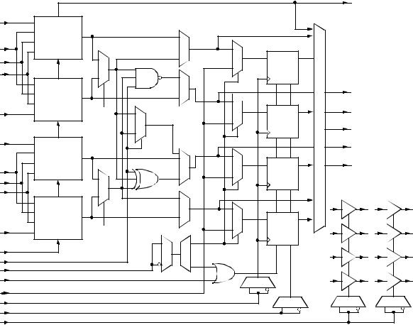
Figure 1. Series 2 Array
4 |
Lucent Technologies Inc. |

Data Sheet |
|
June 1999 |
ORCA Series 2 FPGAs |
ORCA Foundry Development System
Overview
The ORCA Foundry Development System interfaces to front-end design entry tools and provides the tools to produce a configured FPGA. In the design flow, the user defines the functionality of the FPGA at two points: at design entry and at the bit stream generation stage.
Following design entry, the development system’s map, place, and route tools translate the netlist into a routed FPGA. Its bit stream generator is then used to generate the configuration data which is loaded into the FPGA’s internal configuration RAM. When using the bit stream generator, the user selects options that affect the functionality of the FPGA. Combined with the front-end tools, ORCA Foundry produces configuration data that implements the various logic and routing options discussed in this data sheet.
Architecture
The ORCA Series FPGA is comprised of two basic elements: PLCs and PICs. Figure 1 shows an array of programmable logic cells (PLCs) surrounded by programmable input/output cells (PICs). The Series 2 has PLCs arranged in an array of 20 rows and 20 columns. PICs are located on all four sides of the FPGA between the PLCs and the IC edge.
The location of a PLC is indicated by its row and column so that a PLC in the second row and third column is R2C3. PICs are indicated similarly, with PT (top) and PB (bottom) designating rows and PL (left) and PR (right) designating columns, followed by a number. The routing resources and configuration RAM are not shown, but the interquad routing blocks (hIQ, vIQ) present in the Series 2 series are shown.
Each PIC contains the necessary I/O buffers to interface to bond pads. The PICs also contain the routing resources needed to connect signals from the bond pads to/from PLCs. The PICs do not contain any useraccessible logic elements, such as flip-flops.
Combinatorial logic is done in look-up tables (LUTs) located in the PFU. The PFU can be used in different modes to meet different logic requirements. The LUT’s configurable medium-/large-grain architecture can be used to implement from one to four combinatorial logic functions. The flexibility of the LUT to handle wide input functions, as well as multiple smaller input functions, maximizes the gate count/PFU.
The LUTs can be programmed to operate in one of three modes: combinatorial, ripple, or memory. In com-
Lucent Technologies Inc.
binatorial mode, the LUTs can realize any four-, five-, or six-input logic functions. In ripple mode, the highspeed carry logic is used for arithmetic functions, the new multiplier function, or the enhanced data path functions. In memory mode, the LUTs can be used as a 16 x 4 read/write or read-only memory (asynchronous mode or the new synchronous mode) or a new 16 x 2 dual-port memory.
Programmable Logic Cells
The programmable logic cell (PLC) consists of a programmable function unit (PFU) and routing resources. All PLCs in the array are identical. The PFU, which contains four LUTs and four latches/FFs for logic implementation, is discussed in the next section.
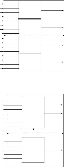
Programmable Function Unit
The PFUs are used for logic. Each PFU has 19 external inputs and six outputs and can operate in several modes. The functionality of the inputs and outputs depends on the operating mode.
The PFU uses three input data buses (A[4:0], B[4:0], WD[3:0]), four control inputs (C0, CK, CE, LSR), and a carry input (CIN); the last is used for fast arithmetic functions. There is a 5-bit output bus (O[4:0]) and a carry-out (COUT).
PROGRAMMABLE LOGIC CELL (PLC)
WD3
WD2
WD1 |
|
COUT |
|
|
|
WD0 |
|
|
A4 |
|
O4 |
A3 |
|
O3 |
A2 |
PROGRAMMABLE |
O2 |
A1 |
FUNCTION UNIT |
O1 |
A0 |
(PFU) |
O0 |
|
||
B4 |
|
|
B3 |
|
|
B2 |
|
|
B1 |
|
|
B0 |
|
|
CIN |
C0 CK CE LSR |
|
(ROUTING RESOURCES, CONFIGURATION RAM)
5-2750(F).r3
Figure 2. PFU Ports
5
|
Data Sheet |
ORCA Series 2 FPGAs |
June 1999 |
|
|
Programmable Logic Cells (continued))
|
|
|
|
|
|
|
|
|
COUT |
|
|
CARRY |
|
|
|
|
|
|
|
A4 |
A4 |
|
|
|
|
|
|
|
|
|
A3 |
QLUT3 |
|
|
|
|
|
|
|
|
A2 |
|
F3 |
|
|
|
|
|
|
A3 |
|
|
|
|
|
|
|
||
A1 |
|
|
C |
D3 |
|
Q3 |
|
|
|
|
|
|
|
|
|
|
|||
|
|
|
|
|
|
|
|
|
|
A2 |
|
|
|
WD3 |
REG3 |
|
|
|
|
|
|
|
|
|
|
|
|
||
A1 |
|
CARRY |
|
|
SR |
EN |
|
|
|
|
A3 |
|
|
F2 |
|
|
|
||
|
|
|
|
|
|
|
|
||
|
A2 |
|
PFU_NAND |
C |
|
|
|
|
O4 |
|
QLUT2 |
|
|
|
|
|
|||
|
A1 |
|
|
|
|
Q2 |
|
|
|
|
A4 |
|
|
D2 |
|
|
O3 |
||
A0 |
A0 |
|
WD2 |
REG2 |
|
|
|||
|
|
|
|
|
|||||
|
|
|
|
|
C |
|
|||
|
|
CARRY |
|
|
|
|
|
O2 |
|
|
|
|
|
SR |
EN |
|
|
||
|
|
|
|
|
|
|
|||
|
|
|
|
|
|
|
|
||
B4 |
B4 |
|
|
|
|
|
|
|
O1 |
|
B3 |
|
PFU_MUX |
F1 |
|
|
|
|
|
|
QLUT1 |
D1 |
|
Q1 |
|
|
|||
|
B2 |
|
|
|
|
O0 |
|||
|
|
|
C |
|
|
|
|
||
B3 |
|
|
|
REG1 |
|
|
|||
B1 |
|
|
|
|
|
||||
|
|
WD1 |
|
|
|
||||
B2 |
|
|
|
|
SR |
EN |
|
|
|
B1 |
|
CARRY |
|
|
|
|
|
||
|
PFU_XOR |
|
|
|
|
|
|
||
|
|
|
|
|
|
|
|
||
|
B3 |
|
|
F0 |
|
|
|
T |
T |
|
B2 |
QLUT0 |
|
C |
D0 |
|
Q0 |
||
|
|
|
|
|
|
|
|||
|
B1 |
|
|
|
|
|
|
|
|
|
|
|
WD0 |
REG0 |
|
|
|
||
B0 |
B0 |
B4 |
|
|
|
|
|||
|
|
SR |
EN |
|
T |
T |
|||
|
|
|
|
|
|
|
|
||
CIN |
|
|
C |
C |
|
|
|
T |
T |
|
|
|
|
|
|
||||
C0 |
|
|
|
|
|
|
|
||
|
|
|
|
|
|
|
|
|
|
LSR |
|
|
|
|
|
|
|
|
|
GSR |
|
|
|
|
C |
|
|
T |
T |
WD[3:0] |
|
|
|
|
|
|
|
|
|
CK |
|
|
|
|
|
C |
|
C |
C |
CKEN |
|
|
|
|
|
|
|
|
|
TRI |
|
|
|
|
|
|
|
|
|
5-4573(F)
Key: C = controlled by configuration RAM.
Figure 3. Simplified PFU Diagram
Figure 2 and Figure 3 show high-level and detailed views of the ports in the PFU, respectively. The ports are referenced with a twoto four-character suffix to a PFU’s location. As mentioned, there are two 5-bit input data buses (A[4:0] and B[4:0]) to the LUT, one 4-bit input data bus (WD[3:0]) to the latches/FFs, and an output data bus (O[4:0]).
Figure 3 shows the four latches/FFs (REG[3:0]) and the 64-bit look-up table (QLUT[3:0]) in the PFU. The PFU does combinatorial logic in the LUT and sequential logic in the latches/FFs. The LUT is static random access memory (SRAM) and can be used for read/ write or read-only memory. The eight 3-state buffers
found in each PLC are also shown, although they actually reside external to the PFU.
Each latch/FF can accept data from the LUT. Alternatively, the latches/FFs can accept direct data from WD[3:0], eliminating the LUT delay if no combinatorial function is needed. The LUT outputs can bypass the latches/FFs, which reduces the delay out of the PFU. It is possible to use the LUT and latches/FFs more or less independently. For example, the latches/FFs can be used as a 4-bit shift register, and the LUT can be used to detect when a register has a particular pattern in it.
6 |
Lucent Technologies Inc. |

Data Sheet |
|
June 1999 |
ORCA Series 2 FPGAs |
Programmable Logic Cells (continued)
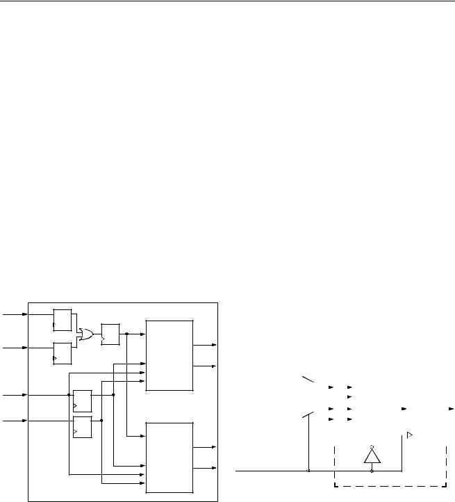
Table 3 lists the basic operating modes of the LUT. The operating mode affects the functionality of the PFU input and output ports and internal PFU routing. For example, in some operating modes, the WD[3:0] inputs are direct data inputs to the PFU latches/FFs. In the dual 16 x 2 memory mode, the same WD[3:0] inputs are used as a 4-bit data input bus into LUT memory.
The PFU is used in a variety of modes, as illustrated in Figures 4 through 11, and it is these specific modes that are most relevant to PFU functionality.
PFU Control Inputs
The four control inputs to the PFU are clock (CK), local set/reset (LSR), clock enable (CE), and C0. The CK, CE, and LSR inputs control the operation of all four latches in the PFU. An active-low global set/reset (GSRN) signal is also available to the latches/FFs in every PFU. Their operation is discussed briefly here, and in more detail in the Latches/Flip-Flops section. The polarity of the control inputs can be inverted.
The CK input is distributed to each PFU from a vertical or horizontal net. The CE input inhibits the latches/FFs from responding to data inputs. The CE input can be disabled, always enabling the clock. Each latch/FF can be independently programmed to be set or reset by the LSR and the global set/reset (GSRN) signals. Each PFU’s LSR input can be configured as synchronous or asynchronous. The GSRN signal is always asynchronous. The LSR signal applies to all four latches/FFs in a PFU. The LSR input can be disabled (the default). The asynchronous set/reset is dominant over clocked inputs.
The C0 input is used as an input into the special PFU gates for wide functions in combinatorial logic mode. In the memory modes, this input is also used as the write-port enable input. The C0 input can be disabled (the default).
Look-Up Table Operating Modes
The look-up table (LUT) can be configured to operate in one of three general modes:
■Combinatorial logic mode
■Ripple mode
■Memory mode
The combinatorial logic mode uses a 64-bit look-up table to implement Boolean functions. The two 5-bit logic inputs, A[4:0] and B[4:0], and the C0 input are
used as LUT inputs. The use of these ports changes based on the PFU operating mode.
The functionality of the LUT is determined by its operating mode. The entries in Table 3 show the basic modes of operation for combinatorial logic, ripple, and memory functions in the LUT. Depending on the operating mode, the LUT can be divided into sub-LUTs. The LUT is comprised of two 32-bit half look-up tables, HLUTA and HLUTB. Each half look-up table (HLUT) is comprised of two quarter look-up tables (QLUTs). HLUTA consists of QLUT2 and QLUT3, while HLUTB consists of QLUT0 and QLUT1. The outputs of QLUT0, QLUT1, QLUT2, and QLUT3 are F0, F1, F2, and F3, respectively.
Table 3. Look-Up Table Operating Modes
Mode |
Function |
|
|
F4A |
Two functions of four inputs, some inputs |
|
shared (QLUT2/QLUT3) |
|
|
F4B |
Two functions of four inputs, some inputs |
|
shared (QLUT0/QLUT1) |
|
|
F5A |
One function of five inputs (HLUTA) |
|
|
F5B |
One function of five inputs (HLUTB) |
|
|
R |
4-bit ripple (LUT) |
|
|
MA |
16 x 2 asynchronous memory (HLUTA) |
|
|
MB |
16 x 2 asynchronous memory (HLUTB) |
|
|
SSPM |
16 x 4 synchronous single-port memory |
|
|
SDPM |
16 x 2 synchronous dual-port memory |
|
|
For combinatorial logic, the LUT can be used to do any single function of six inputs, any two functions of five inputs, or four functions of four inputs (with some inputs shared), and three special functions based on the two five-input functions and C0.
Lucent Technologies Inc. |
7 |
|
Data Sheet |
ORCA Series 2 FPGAs |
June 1999 |
|
|
Programmable Logic Cells (continued)
The LUT ripple mode operation offers standard arithmetic functions, such as 4-bit adders, subtractors, adder/subtractors, and counters. In the ORCA Series 2, there are two new ripple modes available.
The first new mode is a 4 x 1 multiplier, and the second is a 4-bit comparator. These new modes offer the advantages of faster speeds as well as denser logic capabilities.
When the LUT is configured to operate in the memory mode, a 16 x 2 asynchronous memory fits into an HLUT. Both the MA and MB modes were available in previous ORCA architectures, and each mode can be configured in an HLUT separately. In the Series 2, there are two new memory modes available. The first is a 16 x 4 synchronous single-port memory (SSPM), and the second is a 16 x 2 synchronous dual-port memory (SDPM). These new modes offer easier implementation, faster speeds, denser RAMs, and a dual-port capability that wasn’t previously offered as an option in the ATT2Cxx/ATT2Txx families.
If the LUT is configured to operate in the ripple mode, it cannot be used for basic combinatorial logic or memory functions. In modes other than the ripple, SSPM, and SDPM modes, combinations of operating modes are possible. For example, the LUT can be configured as a 16 x 2 RAM in one HLUT and a five-input combinatorial logic function in the second HLUT. This can be done by configuring HLUTA in the MA mode and HLUTB in the F5B mode (or vice versa).
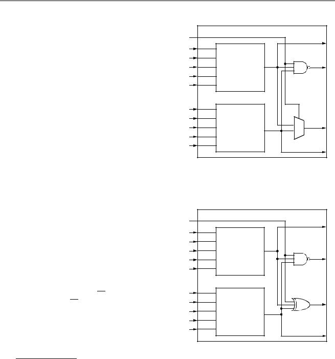
F4A/F4B Mode—Two Four-Input Functions
Each HLUT can be used to implement two four-input combinatorial functions, but the total number of inputs into each HLUT cannot exceed five. The two QLUTs within each HLUT share three inputs. In HLUTA, the A1, A2, and A3 inputs are shared by QLUT2 and QLUT3. Similarly, in HLUTB, the B1, B2, and B3 inputs are shared by QLUT0 and QLUT1. The four outputs are F0, F1, F2, and F3. The results can be routed to the D0, D1, D2, and D3 latch/FF inputs or as an output of the PFU. The use of the LUT for four functions of up to four inputs each is given in Figure 4.
F5A/F5B Mode—One Five-Input Variable Function
Each HLUT can be used to implement any five-input combinatorial function. The input ports are A[4:0] and B[4:0], and the output ports are F0 and F3. One five or less input function is input into A[4:0], and the second five or less input function is input into B[4:0]. The results are routed to the latch/FF D0 and latch/FF D3 inputs, or as a PFU output. The use of the LUT for two
8
independent functions of up to five inputs is shown in Figure 5. In this case, the LUT is configured in the F5A and F5B modes. As a variation, the LUT can do one function of up to five input variables and two four-input functions using F5A and F4B modes or F4A and F5B modes.
A4 |
A4 |
|
HLUTA |
|
|
||
A3 |
A3 |
QLUT3 |
F3 |
A2 |
A2 |
|
|
|
|
||
A1 |
A1 |
|
|
A3 |
A3 |
|
|
A2 |
A2 |
QLUT2 |
F2 |
A1 |
A1 |
|
|
|
|
||
A0 |
A0 |
|
|
B4 |
B4 |
|
HLUTB |
B3 |
B3 |
QLUT1 |
F1 |
B2 |
B2 |
|
|
|
|
||
B1 |
B1 |
|
|
B3 |
B3 |
|
|
B2 |
B2 |
QLUT0 |
F0 |
B1 |
B1 |
|
|
|
|
||
B0 |
B0 |
|
|
|
|
|
5-2753(F).r2 |
Figure 4. F4 Mode—Four Functions of Four-
Input Variables
|
|
HLUTA |
|
WEA |
A4 |
F3 |
|
A3 |
A3 |
||
QLUT3 |
|||
A2 |
A2 |
F2 |
|
|
A1 |
||
A1 |
QLUT2 |
||
A0 |
A0 |
|
|
WD3 |
WD3 |
|
|
WD2 |
WD2 |
c0 |
|
WPE |
|
|
|
|
|
HLUTB |
|
B4 |
B4 |
|
|
B3 |
B3 |
QLUT1 |
|
B2 |
B2 |
F0 |
|
|
|||
B1 |
B1 |
QLUT0 |
|
|
|
||
B0 |
B0 |
|
|
|
|
5-2845(F).r2 |
Figure 5. F5 Mode—Two Functions of Five-Input
Variables
Lucent Technologies Inc.
Data Sheet |
|
June 1999 |
ORCA Series 2 FPGAs |
Programmable Logic Cells (continued)
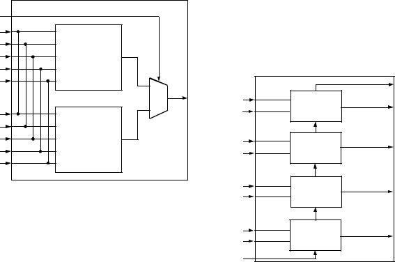
F5M and F5X Modes—Special Function Modes
The PFU contains logic to implement two special function modes which are variations on the F5 mode. As with the F5 mode, the LUT implements two independent five-input functions. Figure 6 and Figure 7 show the schematics for F5M and F5X modes, respectively. The F5X and F5M functions differ from the basic F5A/ F5B functions in that there are three logic gates which have inputs from the two 5-input LUT outputs. In some cases, this can be used for faster and/or wider logic functions.
As can be seen, two of the three inputs into the NAND, XOR, and MUX gates, F0 and F3, are from the LUT. The third input is from the C0 input into PFU. Since the C0 input bypasses the LUTs, it has a much smaller delay through the PFU than for all other inputs into the special PFU gates. This allows multiple PFUs to be cascaded together while reducing the delay of the critical path through the PFUs. The output of the first special function (either XOR or MUX) is F1. Since the XOR and MUX share the F1 output, the F5X and F5M modes are mutually exclusive. The output of the NAND PFU gate is F2 and is always available in either mode.
To use either the F5M or F5X functions, the LUT must be in the F5A/F5B mode; i.e., only 5-input LUTs allowed. In both the F5X and F5M functions, the outputs of the five-input combinatorial functions, F0 and F3, are also usable simultaneously with the special PFU gate outputs.
The output of the MUX is:
F1 = (HLUTA & C0) + (HLUTB & C0)
F1 = (F3 & C0) + (F0 & C0)
The output of the exclusive OR is:
F1 = HLUTA Å HLUTB Å C0
F1 = F3 Å F0 Å C0
The output of the NAND is:
F2 = HLUTA & HLUTB & C0
F2 = F3 & F0 & C0
C0 |
|
|
F3 |
|
|
|
|
||
A4 |
A4 |
|
|
|
A3 |
A3 |
QLUT3 |
F2 |
|
A2 |
A2 |
F3 |
||
|
||||
|
|
|||
A1 |
A1 |
QLUT2 |
|
|
A0 |
A0 |
|
|
|
B4 |
B4 |
|
|
|
B3 |
B3 |
QLUT1 |
F1 |
|
B2 |
B2 |
F0 |
||
|
||||
B1 |
B1 |
QLUT0 |
|
|
B0 |
B0 |
|
F0 |
|
|
|
|
||
|
|
|
5-2754(F).r3 |
Figure 6. F5M Mode—Multiplexed Function of Two
Independent Five-Input Variable
Functions
C0 |
|
F3 |
|
|
|
||
A4 |
A4 |
HLUTA |
|
|
|
||
A3 |
A3 |
F3 |
|
A2 |
A2 |
||
F2 |
|||
A1 |
A1 |
||
|
|||
A0 |
A0 |
|
|
B4 |
B4 |
HLUTB |
|
|
|
||
B3 |
B3 |
F1 |
|
B2 |
B2 |
F0 |
|
B1 |
B1 |
|
|
B0 |
B0 |
F0 |
|
|
|
||
|
|
5-2755(F).r2 |
Figure 7. F5X Mode—Exclusive OR Function of Two
Independent Five-Input Variable
Functions
Lucent Technologies Inc. |
9 |
|
Data Sheet |
ORCA Series 2 FPGAs |
June 1999 |
|
|
Programmable Logic Cells (continued)
C0 |
|
|
A4 |
A4 |
|
A3 |
A3 |
QLUT3 |
A2 |
A2 |
F3 |
|
||
A1 |
A1 |
QLUT2 |
A0 |
A0 |
|
|
|
F1 |
B4 |
B4 |
|
B3 |
B3 |
QLUT1 |
B2 |
B2 |
F0 |
|
||
B1 |
B1 |
QLUT0 |
B0 |
B0 |
|
|
|
5-2751(F).r3 |
Figure 8. F5M Mode—One Six-Input Variable
Function
F5M Mode—One Six-Input Variable Function
The LUT can be used to implement any function of sixinput variables. As shown in Figure 8, five input signals (A[4:0]) are routed into both the A[4:0] and B[4:0] ports, and the C0 port is used for the sixth input. The output port is F1.
Ripple Mode
The LUT can do nibble-wide ripple functions with highspeed carry logic. Each QLUT has a dedicated carryout net to route the carry to/from the adjacent QLUT. Using the internal carry circuits, fast arithmetic and counter functions can be implemented in one PFU. Similarly, each PFU has carry-in (CIN) and carry-out (COUT) ports for fast-carry routing between adjacent PFUs.
The ripple mode is generally used in operations on two 4-bit buses. Each QLUT has two operands and a ripple (generally carry) input, and provides a result and ripple (generally carry) output. A single bit is rippled from the previous QLUT and is used as input into the current QLUT. For QLUT0, the ripple input is from the PFU CIN port. The CIN data can come from either the fast-carry routing or the PFU input B4, or it can be tied to logic 1 or logic 0.
The resulting output and ripple output are calculated by using generate/propagate circuitry. In ripple mode, the
two operands are input into A[3:0] and B[3:0]. The four result bits, one per QLUT, are F[3:0] (see Figure 9). The ripple output from QLUT3 can be routed to dedicated carry-out circuitry into any of four adjacent PLCs, or it can be placed on the O4 PFU output, or both. This allows the PLCs to be cascaded in the ripple mode so that nibble-wide ripple functions can be expanded easily to any length.
|
|
|
COUT |
B3 |
B3 |
COUT |
F3 |
A3 |
A3 |
QLUT3 |
|
B2 |
B2 |
QLUT2 |
F2 |
A2 |
A2 |
|
|
B1 |
B1 |
QLUT1 |
F1 |
A1 |
A1 |
|
|
B0 |
B0 |
QLUT0 |
F0 |
A0 |
A0 |
|
|
CIN |
|
||
|
|
|
|
CIN |
|
|
|
|
|
|
5-2756(F).r32 |
Figure 9. Ripple Mode
The ripple mode can be used in one of four submodes. The first of these is adder/subtractor mode. In this mode, each QLUT generates two separate outputs. One of the two outputs selects whether the carry-in is to be propagated to the carry-out of the current QLUT or if the carry-out needs to be generated. The result of this selection is placed on the carry-out signal, which is connected to the next QLUT or the COUT signal, if it is the last QLUT (QLUT3).
The other QLUT output creates the result bit for each QLUT that is connected to F[3:0]. If an adder/subtractor is needed, the control signal to select addition or subtraction is input on A4. The result bit is created in onehalf of the QLUT from a single bit from each input bus, along with the ripple input bit. These inputs are also used to create the programmable propagate.
10 |
Lucent Technologies Inc. |
Data Sheet |
|
June 1999 |
ORCA Series 2 FPGAs |
Programmable Logic Cells (continued)
The second submode is the counter submode (see Figure 10). The present count is supplied to input A[3:0], and then output F[3:0] will either be incremented by one for an up counter or decremented by one for a down counter. If an up counter or down counter is needed, the control signal to select the direction (up or down) is input on A4. Generally, the latches/ FFs in the same PFU are used to hold the present count value.
|
LUT |
|
|
|
|
|
|
|
COUT |
A3 |
COUT |
F3 |
|
Q3 |
|
QLUT3 |
D |
Q |
|
A2 |
QLUT2 |
F2 |
Q |
Q2 |
|
D |
|||
A1 |
QLUT1 |
F1 |
Q |
Q1 |
|
D |
|||
A0 |
QLUT0 |
F0 |
|
Q0 |
|
D |
Q |
||
|
CIN |
|||
|
|
|
|
|
CIN |
|
|
|
|
|
|
|
|
5-4643(F).r1 |
Figure 10. Counter Submode with Flip-Flops
In the third submode, multiplier submode, a single PFU can affect a 4 x 1-bit multiply and sum with a partial product (see Figure 11). The multiplier bit is input at A4, and the multiplicand bits are input at B[3:0], where B3 is the most significant bit (MSB). A[3:0] contains the partial product (or other input to be summed) from a previous stage. If A4 is logical 1, the multiplicand is added to the partial product. If A4 is logical zero, zero is added to the partial product, which is the same as passing the partial product. CIN can hold the carry-in from the less significant PFUs if the multiplicand is wider than 4 bits, and COUT holds any carry-out from the addition, which may then be used as part of the product or routed to another PFU in multiplier mode for multiplicand width expansion.
A3 |
B3 |
|
A2 |
B2 |
|
A1 |
B1 |
|
A0 |
B0 |
|
|
|
0 |
|
|
0 |
|
|
0 |
|
|
0 |
|
1 |
0 |
|
1 |
0 |
|
1 |
0 |
|
1 |
0 |
A4 |
|
|
|
|
|
|
|
|
|
|
|
COUT |
+ |
|
|
+ |
|
|
+ |
|
|
+ |
CIN |
|
F3 |
|
|
F2 |
|
|
F1 |
|
|
F0 |
5-4620(F) |
|
|
|
|
|
|
|
|
|
|
|
Figure 11. Multiplier Submode
Ripple mode’s fourth submode features equality comparators, where one 4-bit bus is input on B[3:0], another 4-bit bus is input on B[3:0], and the carry-in is tied to 0 inside the PFU. The carry-out (¦)signal will be 0 if A = B or will be 1 if A ¦ B. If larger than 4 bits, the carry-out (¦)signal can be cascaded using fast-carry logic to the carry-in of any adjacent PFU. Comparators for greater than or equal or less than (>, =, <) continue to be supported using the ripple mode subtractor. The use of this submode could be shown using Figure 9 with CIN tied to 0.
Lucent Technologies Inc. |
11 |
|
Data Sheet |
ORCA Series 2 FPGAs |
June 1999 |
|
|
Programmable Logic Cells (continued)
Asynchronous Memory Modes—MA and MB
The LUT in the PFU can be configured as either read/ write or read-only memory. A read/write address (A[3:0], B[3:0]), write data (WD[1:0], WD[3:2]), and two write-enable (WE) ports are used for memory. In asynchronous memory mode, each HLUT can be used as a 16 x 2 memory. Each HLUT is configured independently, allowing functions such as a 16 x 2 memory in one HLUT and a logic function of five input variables or less in the other HLUT.
Figure 12 illustrates the use of the LUT for a 16 x 4 memory. When the LUTs are used as memory, there are independent address, input data, and output data buses. If the LUT is used as a 16 x 4 read/write memory, the A[3:0] and B[3:0] ports are address inputs (A[3:0]). The A4 and B4 ports are write-enable (WE) signals. The WD[3:0] inputs are the data inputs. The F[3:0] data outputs can be routed out on the O[4:0] PFU outputs or to the latch/FF D[3:0] inputs.
WEA |
A4 |
|
HLUTA |
A3 |
A3 |
|
|
A2 |
A2 |
|
F3 |
A1 |
A1 |
|
|
|
F2 |
||
A0 |
A0 |
|
|
|
|
||
WD3 |
WD3 |
|
|
WD2 |
WD2 C0 |
|
|
WPE |
|
|
|
WEB |
B4 |
C0 |
HLUTB |
WD1 |
WD1 |
|
|
WD0 |
WD0 |
|
F1 |
B3 |
B3 |
|
|
|
|
||
B2 |
B2 |
|
F0 |
|
|
||
B1 |
B1 |
|
|
B0 |
B0 |
|
|
|
|
|
5-2757(F).r3 |
|
Figure 12. MA/MB Mode—16 x 4 RAM |
||
To increase memory word depth above 16 (e.g., 32 x 4), two or more PLCs can be used. The address and write data inputs for the two or more PLCs are tied together (bit by bit), and the data outputs are routed through the four 3-statable BIDIs available in each PFU and are then tied together (bit by bit).
The control signal of the 3-statable BIDIs, called a RAM bank-enable, is created from a decode of upper address bits. The RAM bank-enable is then used to
12
enable 4 bits of data from a PLC onto the read data bus.
The ORCA Series 2 series also has a new AND function available for each PFU in RAM mode. The inputs to this function are the write-enable (WE) signal and the write-port enable (WPE) signal. The write-enable signal is A4 for HLUTA and B4 for HLUTB, while the other input into the AND gates for both HLUTs is the writeport enable, input on C0 or CIN. Generally, the WPE input is driven by the same RAM bank-enable signal that controls the BIDIs in each PFU.
The selection of which RAM bank to write data into does not require the use of LUTs from other PFUs, as in previous ORCA architectures. This reduces the number of PFUs required for RAMs larger than 16 words in depth. Note that if either HLUT is in MA/MB mode, then the same WPE is active for both HLUTs.
To increase the memory’s word size (e.g., 16 x 8), two or more PLCs are used again. The address, writeenable, and write-port enable of the PLCs are tied together (bit by bit), and the data is different for each PLC. Increasing both the address locations and word size is done by using a combination of these two techniques.
The LUT can be used simultaneously for both memory and a combinatorial logic function. Figure 13 shows the use of a LUT implementing a 16 x 2 RAM (HLUTA) and any function of up to five input variables (HLUTB).
|
|
|
HLUTA |
|
WEA |
A4 |
|
F3 |
|
A3 |
A3 |
QLUT3 |
||
|
||||
A2 |
A2 |
|
|
|
A1 |
A1 |
QLUT2 |
F2 |
|
|
||||
A0 |
A0 |
|
|
|
WD3 |
WD3 |
C0 |
|
|
|
|
|
||
WPE |
|
|
|
|
|
|
|
HLUTB |
|
B4 |
B4 |
|
|
|
B3 |
B3 |
QLUT1 |
F0 |
|
B2 |
B2 |
|
||
|
|
|||
B1 |
B1 |
QLUT0 |
|
|
|
|
|
||
B0 |
B0 |
|
|
|
|
|
|
5-2845(F).a.r1 |
Figure 13. MA/F5 Mode—16 x 2 Memory and One Function of Five Input Variables
Lucent Technologies Inc.
Data Sheet |
|
June 1999 |
ORCA Series 2 FPGAs |
Programmable Logic Cells (continued)
Synchronous Memory Modes—SSPM and SDPM
The MA/MB asynchronous memory modes described previously allow the PFU to perform as a 16 x 4
(64 bits) single-port RAM. Synchronously writing to this RAM requires the write-enable control signal to be gated with the clock in another PFU to create a write pulse. To simplify this functionality, the Series 2 devices contain a synchronous single-port memory (SSPM) mode, where the generation of the write pulse is done in each PFU.
With SSPM mode, the entire LUT becomes a 16 x 4 RAM, as shown in Figure 14. In this mode, the input ports are write enable (WE), write-port enable (WPE), read/write address (A[3:0]), and write data (WD[3:0]). To synchronously write the RAM, WE (input into a4) and WPE (input into either C0 or CIN) are latched and ANDed together. The result of this AND function is sent to a pulse generator in the LUT, which writes the RAM synchronous to the RAM clock. This RAM clock is the same one sent to the PFU latches/FFs; however, if necessary, it can be programmably inverted.
WE |
A4 |
D Q |
WRITE PULSE |
|
|
|
|
GENERATOR |
|
||
|
|
|
|
|
|
|
|
|
|
HLUTA |
|
|
|
|
|
WR |
F3 |
WPE |
CIN, C0 |
|
|
|
|
D |
Q |
|
|
||
|
|
|
|
WA[3:0] |
F2 |
|
|
|
|
|
|
|
|
|
|
RA[3:0] |
|
A[3:0] |
|
|
|
WD[3:2] |
|
A[3:0], B[3:0] |
D Q |
|
|||
|
|
|
|
|
|
WD[3:0] WD[3:0] |
|
|
D Q |
|
|
|
|
|
|
HLUTB |
|
|
|
|
|
WR |
F1 |
|
|
|
|
|
|
|
|
|
|
WA[3:0] |
F0 |
|
|
|
|
|
|
|
|
|
|
RA[3:0] |
|
|
|
|
|
WD[1:0] |
|
|
|
|
|
|
5-4642(F).r1 |
Figure 14. SSPM Mode—16 x 4 Synchronous
Single-Port Memory
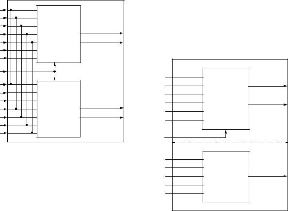
The write address (WA[3:0]) and write data (WD[3:0]) are also latched by the RAM clock in order to simplify the timing. Reading data from the RAM is done asynchronously; thus, the read address (RA[3:0]) is not latched. The result from the read operation is placed on the LUT outputs (F[3:0]). The F[3:0] data outputs can be routed out of the PFU or sent to the latch/FF D[3:0] inputs.
There are two ways to use the latches/FFs in conjunction with the SSPM. If the phase of the latch/FF clock and the RAM clock are the same, only a read address or write address can be supplied to the RAM that meets the synchronous timing requirements of both the RAM clock and latch/FF clock. Therefore, either a write to the RAM or a read from the RAM can be done in each clock cycle, but not both. If the RAM clock is inverted from the latch/FF clock, then both a write to the RAM and a read from the RAM can occur in each clock cycle. This is done by adding an external write address/read address multiplexer as shown in
Figure 15.
The write address is supplied on the phase of the clock that allows for setup to the RAM clock, and the read address is supplied on the phase of the clock that allows the read data to be set up to the latch/FF clock. If a higher-speed RAM is required that allows both a read and write in each clock cycle, the synchronous dual-port memory mode (SDPM) can be used, since it does not require the use of an external multiplexer.
|
|
|
|
|
|
|
|
|
|
|
|
|
|
|
|
|
|
|
|
|
|
|
|
|
|
|
|
|
|
WRITE ADDRESS |
|
|
|
|
|
|
|
|
|
|
|
SSPM |
|
|
|
|
|
|
|
|
|
|
|
|
|
|
|||
|
|
|
|
|
|
|
|
|
|
|
|
|
|
|
|
|
|
|
|
|
|
|
|
|
|
|
|
|
|
1 |
|
|
|
|
|
|
|
|
WD |
|
|
|
|
|
|
|
|
|
|
|
|
|
|
||||||
|
|
|
|
|
|
|
|
|
|
|
|
|
|
|
|
|
|
|
|
|
|
|
|||||||
READ ADDRESS |
0 |
|
|
|
|
|
|
|
|
A |
|
|
|
|
|
|
|
|
|
|
|
|
|
|
|||||
|
|
|
|
|
|
|
|
|
|
|
|
|
|
|
|
|
|
|
|
|
|
||||||||
|
|
|
|
|
|
|
|
WE |
|
|
|
|
|
D |
|
|
Q |
|
|
|
|
||||||||
|
|
|
|
|
|
|
|
|
|
|
|
|
|
|
|
|
|
|
|
||||||||||
|
|
|
|
|
|
|
|
|
|
|
|
|
|
|
|
|
|
|
|
||||||||||
|
|
|
|
|
|
|
|
|
|
|
|
|
|
|
|
|
|
|
|
|
|||||||||
|
|
|
|
|
|
|
|
|
|
WPE |
|
|
|
|
|
|
|
|
|
|
|
|
|
|
|||||
|
|
|
|
|
|
|
|
|
|
|
|
|
|
|
|
|
|
|
|
|
|
|
|
||||||
|
|
|
|
|
|
|
|
|
|
|
RAM CLK |
|
|
|
|
|
|
|
|
|
|
|
|
|
|
||||
|
|
|
|
|
|
|
|
|
|
|
|
|
|
|
|
|
|
|
|
|
|
|
|
|
|||||
|
|
|
|
|
|
|
|
|
|
|
|
|
|
|
|
|
|
|
|
|
|
|
|
|
|
|
|
|
|
|
|
|
|
|
|
|
|
|
|
|
|
|
|
|
|
|
|
|
|
|
|
|
|
|
|
|
|
|
|
|
|
|
|
|
|
|
|
|
|
|
|
|
|
|
|
|
|
|
|
|
|
|
|
|
|
|
|
|
|
CLOCK
PFU
5-4644(F).r1
Figure 15. SSPM with Read/Write per Clock Cycle
Lucent Technologies Inc. |
13 |
|
Data Sheet |
ORCA Series 2 FPGAs |
June 1999 |
|
|
Programmable Logic Cells (continued)
|
|
|
|
|
|
|
|
|
|
|
|
|
|
|
|
|
UPPER |
ADDRESS |
BANK_EN1 |
|
|
|
|
|
|
|
|
|
|
|
|||
ADDRESS |
|
|
DECODE |
|
|
|
|
|
|
|
|
|
|
|
||
|
|
|
|
|
|
|
|
|
|
|
|
|
|
|||
BITS |
LUT1 |
|
|
|
|
|
|
|
|
|
|
|
|
|||
|
|
|
|
|
|
|
|
|
DI |
WPE |
4 |
|
|
|
|
|
|
|
|
|
|
|
|
|
|
|
|
|
|
|
|||
|
|
|
|
|
|
|
|
|
|
DO |
|
|
|
|
||
|
|
|
|
|
|
|
|
|
|
|
|
|
|
|||
|
|
|
|
|
|
|
|
|
WR |
BIDI |
|
|
|
|||
|
|
|
|
|
|
|
|
|
|
|
|
|||||
|
|
|
|
|
|
|
|
|
|
|
|
|
|
|
||
|
|
|
|
|
|
|
|
|
|
|
|
|
|
|
|
|
|
|
|
|
|
|
|
|
|
|
|
16 x 4 RAM + |
|
4 |
|
||
|
|
|
|
|
|
|
|
|
|
4 BUFFERS/PFU |
DOUT |
|||||
UPPER |
ADDRESS |
BANK_EN2 |
|
|
|
|
|
|
|
|
|
|
||||
|
|
|
|
|
|
|
|
|
|
|
||||||
ADDRESS |
|
|
DECODE |
|
|
|
|
|
|
|
|
|
|
|
||
|
|
|
|
|
|
|
|
|
|
|
|
|
|
|||
BITS |
LUT2 |
|
|
|
|
|
|
|
|
|
|
|
|
|||
|
|
|
|
|
|
|
|
|
|
|
|
|
|
|
|
|
|
|
|
|
|
|
|
|
|
|
WPE |
|
|
|
|
|
|
|
|
|
DIN |
|
4 |
|
|
|
DI |
|
4 |
|
|
|
|
|
|
|
|
|
|
|
|
|
DO |
|
|
|
|
||||
|
|
|
|
|
|
|
|
|
|
|
|
|
||||
|
|
|
WR |
|
|
|
|
|
WR |
BIDI |
|
|
|
|||
|
|
|
|
|
|
|
|
|
|
|
||||||
|
|
|
CLK |
|
|
|
|
|
|
|
|
|
|
|
||
|
|
|
|
|
|
|
|
|
|
|
|
|
|
|
|
|
|
|
|
|
|
|
|
|
|
|
|
|
|
|
|
|
|
|
|
|
|
|
|
|
|
|
|
|
16 x 4 RAM + |
|
|
|
||
|
|
|
|
|
|
|
|
|
|
|
4 BUFFERS/PFU |
|
|
|
||
5-4640(F)
Note: The lower address bits are not shown.
Figure 16. Synchronous RAM with Write-Port Enable (WPE)
To increase memory word depth above 16 (e.g., 32 x 4), two or more PLCs can be used. The address and write data inputs for the two or more PLCs are tied together (bit by bit), and the data outputs are routed through the four 3-statable BIDIs available in each PFU. The BIDI outputs are then tied together (bit by bit), as seen in Figure 16.
The control signals of the 3-statable BIDIs, called RAM bank-enable (BANK_EN1 and BANK_EN2), are created from a decode of upper address bits. The RAM bank-enable is then used to enable 4 bits of data from a PLC onto the read data (DOUT) bus.
The Series 2 series now has a new AND function available for each PFU in RAM mode. The inputs to this function are the write-enable (WE) signal and the writeport enable (WPE) signal. The write-enable signal is input on A4, while the write-port enable is input on C0 or CIN. Generally, the WPE input is driven by the same RAM bank-enable signal that controls the BIDIs in each PFU.
The selection as to which RAM bank to write data into does not require the use of LUTs from other PFUs, as in previous ORCA architectures. This reduces the number of PFUs required for RAMs larger than 16 words in depth.
A special use of this method can be to increase word depth to 32 words. Since both the WPE input into the RAM and the 3-state input into the BIDI can be inverted, a decode of the one upper address bit is not required. Instead, the bank-enable signal for both banks is tied to the upper address bit, with the WPE and 3-state inputs active-high for one bank and activelow for the other.
To increase the memory’s word size (e.g., 16 x 8), two or more PLCs are used again. The address, writeenable, and write-port enable of the PLCs are tied together (bit by bit), and the data is different for each PLC. Increasing both the address locations and word size is accomplished by using a combination of these two techniques.
14 |
Lucent Technologies Inc. |
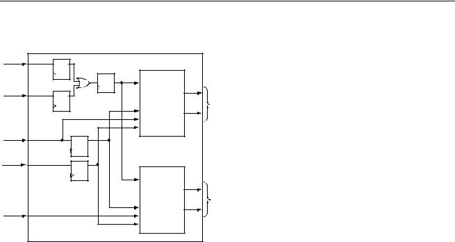
Data Sheet |
|
June 1999 |
ORCA Series 2 FPGAs |
Programmable Logic Cells (continued)
WE |
A4 |
D Q |
WRITE PULSE |
|
|
|
|
|
GENERATOR |
|
|
||
|
|
|
|
|
|
|
|
|
|
|
HLUTA |
|
|
|
|
|
|
WR |
F3 |
SSPM |
WPE |
CIN, C0 |
D |
Q |
|
||
|
|
|||||
|
|
OUTPUT |
||||
|
|
|
|
WA[3:0] |
F2 |
|
|
|
|
|
|
||
|
|
|
|
|
|
|
|
|
|
|
RA[3:0] |
|
|
|
|
|
|
WD[1:0] |
|
|
WA[3:0] |
A[3:0] |
|
|
D Q |
|
|
|
|
|
|
|
|
|
WD[1:0] |
WD[1:0] |
|
|
D Q |
|
|
|
|
|
|
|
|
|
|
|
|
|
HLUTB |
|
|
|
|
|
|
WR |
F1 |
SDPM |
|
|
|
|
|
||
|
|
|
|
|
OUTPUT |
|
RA[3:0] |
B[3:0] |
|
|
WA[3:0] |
F0 |
|
|
|
|
||||
|
|
|
|
|||
|
|
RA[3:0] |
|
|
||
|
|
|
|
|
|
|
|
|
|
|
WD[1:0] |
|
|
|
|
|
|
|
5-4641(F).r1 |
|
Figure 17. SDPM Mode—16 x 2 Synchronous
Dual-Port Memory
The Series 2 devices have added a second synchronous memory mode known as the synchronous dualport memory (SDPM) mode. This mode writes data into the memory synchronously in the same manner described previously for SSPM mode. The SDPM mode differs in that two separate 16 x 2 memories are created in each PFU that have the same WE, WPE, write data (WD[1:0]), and write address (WA[3:0]) inputs, as shown in Figure 17.
The outputs of HLUTA (F[3:2]) operate the same way they do in SSPM mode—the read address comes directly from the A[3:0] inputs used to create the latched write address. The outputs of HLUTB (F[1:0]) operate in a dual-port mode where the write address comes from the latched version of A[3:0], and the read address comes directly from RA[3:0], which is input on B[3:0].
Since external multiplexing of the write address and read address is not required, extremely fast RAMs can be created. New system applications that require an interface between two different asynchronous clocks can also be implemented using the SDPM mode. An example of this is accomplished by creating FIFOs where one clock controls the synchronous write of data into the FIFO, and the other clock controls the read address to allow reading of data at any time from the FIFO.
Latches/Flip-Flops
The four latches/FFs in the PFU can be used in a variety of configurations. In some cases, the configuration options apply to all four latches/FFs in the PFU. For other options, each latch/FF is independently programmable.
Table 4 summarizes these latch/FF options. The latches/FFs can be configured as either positive or negative level-sensitive latches, or positive or negative edge-triggered flip-flops. All latches/FFs in a given PFU share the same clock, and the clock to these latches/ FFs can be inverted. The input into each latch/FF is from either the corresponding QLUT output (F[3:0]) or the direct data input (WD[3:0]). For latches/FFs located in the two outer rings of PLCs, additional inputs are possible. These additional inputs are fast paths from I/O pads located in PICs in the same row or column as the PLCs. If the latch/FF is not located in the two outer rings of the PLCs, the latch/FF input can also be tied to logic 0, which is the default. The four latch/FF outputs, Q[3:0], can be placed on the five PFU outputs, O[4:0].
Table 4. Configuration RAM Controlled Latch/
Flip-Flop Operation
Function |
Options |
|
|
Functionality Common to All Latch/FFs in PFU |
|
|
|
LSR Operation |
Asynchronous or synchronous |
|
|
Clock Polarity |
Noninverted or inverted |
|
|
Front-End Select |
Direct (WD[3:0]) or from LUT |
|
(F[3:0]) |
|
|
LSR Priority |
Either LSR or CE has priority |
|
|
Functionality Set Individually in Each Latch/FF in PFU |
|
|
|
Latch/FF Mode |
Latch or flip-flop |
|
|
Set/Reset Mode |
Set or Reset |
|
|
The four latches/FFs in a PFU share the clock (CK), clock enable (CE), and local set/reset (LSR) inputs. When CE is disabled, each latch/FF retains its previous value when clocked. Both the clock enable and LSR inputs can be inverted to be active-low.
Lucent Technologies Inc. |
15 |
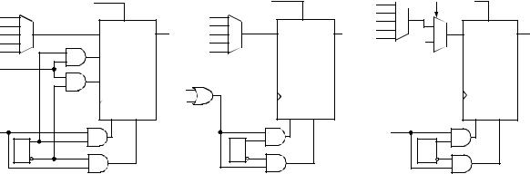
|
Data Sheet |
ORCA Series 2 FPGAs |
June 1999 |
|
|
Programmable Logic Cells (continued)
The set/reset operation of the latch/FF is controlled by two parameters: reset mode and set/reset value. When the global set/reset (GSRN) or local set/reset (LSR) are inactive, the storage element operates normally as a latch or FF. The reset mode is used to select a synchronous or asynchronous LSR operation. If synchronous, LSR is enabled only if clock enable (CE) is active. For the Series 2 series, a new option called the LSR priority allows the synchronous LSR to have priority over the CE input, thereby setting or resetting the FF independent of the state of CE. The clock enable is supported on FFs, not latches. The clock enable function is implemented by using a two-input multiplexer on the FF input, with one input being the previous state of the FF and the other input being the new data applied to the FF. The select of this two-input multiplexer is clock enable (CE), which selects either the new data or the previous state. When CE is inactive, the FF output does not change when the clock edge arrives.
The GSRN signal is only asynchronous, and it sets/ resets all latches/FFs in the FPGA based upon the set/ reset configuration bit for each latch/FF. The set/reset value determines whether GSRN and LSR are set or reset inputs. The set/reset value is independent for each latch/FF.
If the local set/reset is not needed, the latch/FF can be configured to have a data front-end select. Two data inputs are possible in the front-end select mode, with the LSR signal used to select which data input is used. The data input into each latch/FF is from the output of its associated QLUT F[3:0] or direct from WD[3:0], bypassing the LUT. In the front-end data select mode, both signals are available to the latches/FFs.
For PLCs that are in the two outside rows or columns of the array, the latch/FFs can have two inputs in addition to the F and WD inputs mentioned above. One input is from an I/O pad located at the PIC closest to either the left or right of the given PLC (if the PLC is in the left two columns or right two columns of the array). The other input is from an I/O pad located at the closest PIC either above or below the given PLC (if the PLC is in the top or the bottom two rows). It should be noted that both inputs are available for a 2 x 2 array of PLCs in each corner of the array. For the entire array of PLCs, if either or both of these inputs is unavailable, the latch/ FF data input can be tied to a logic 0 instead (the default).
To speed up the interface between signals external to the FPGA and the latches/FFs, there are direct paths from latch/FF outputs to the I/O pads. This is done for each PLC that is adjacent to a PIC.
The latches/FFs can be configured in three modes:
1.Local synchronous set/reset: the input into the PFU’s LSR port is used to synchronously set or reset each latch/FF.
2.Local asynchronous set/reset: the input into LSR asynchronously sets or resets each latch/FF.
3.Latch/FF with front-end select: the data select signal (actually LSR) selects the input into the latches/FFs between the LUT output and direct data in.
For all three modes, each latch/FF can be independently programmed as either set or reset. Each latch/ FF in the PFU is independently configured to operate as either a latch or flip-flop. Figure 18 provides the logic functionality of the front-end select, global set/reset, and local set/reset operations.
|
CE |
|
CE |
|
|
PDINTB |
LSR |
CE |
|
|
|
|
|
|
|
|
|||||
PDINTB |
|
|
PDINTB |
|
|
PDINLR |
|
|
|
|
|
|
|
|
F |
|
|
|
|||
PDINLR |
CE |
|
PDINLR |
CE |
|
|
CE |
|
||
|
|
WD |
|
|
||||||
F |
D |
Q |
F |
D |
Q |
|
D |
Q |
||
LOGIC 0 |
WD |
|||||||||
WD |
|
|
WD |
|
|
|
|
|||
|
|
|
|
|
|
|
||||
LOGIC 0 |
S_SET |
|
LOGIC 0 |
|
|
|
|
|
|
|
|
|
|
|
|
|
|
|
|
||
LSR |
|
|
|
|
|
|
|
|
|
|
|
S_RESET |
|
GSRN |
|
|
|
|
|
|
|
|
CLK |
|
CLK |
|
|
|
CLK |
|
||
|
|
LSR |
|
|
|
|
||||
|
SET RESET |
|
SET RESET |
|
|
SET RESET |
||||
GSRN |
|
|
|
|
|
GSRN |
|
|
|
|
|
CD |
|
CD |
|
|
|
CD |
|
|
|
Note: CD = configuration data.
5-2839(F).a
Figure 18. Latch/FF Set/Reset Configurations
16 |
Lucent Technologies Inc. |

Data Sheet |
|
June 1999 |
ORCA Series 2 FPGAs |
Programmable Logic Cells (continued)
PLC Routing Resources
Generally, the ORCA Foundry Development System is used to automatically route interconnections. Interactive routing with the ORCA Foundry design editor (EPIC) is also available for design optimization. To use EPIC for interactive layout, an understanding of the routing resources is needed and is provided in this section.
The routing resources consist of switching circuitry and metal interconnect segments. Generally, the metal lines which carry the signals are designated as routing nodes (lines). The switching circuitry connects the routing nodes, providing one or more of three basic functions: signal switching, amplification, and isolation. A net running from a PFU or PIC output (source) to a PLC or PIC input (destination) consists of one or more lines, connected by switching circuitry designated as configurable interconnect points (CIPs).
The following sections discuss PLC, PIC, and interquad routing resources. This section discusses the PLC switching circuitry, intra-PLC routing, inter-PLC routing, and clock distribution.
Configurable Interconnect Points
The process of connecting lines uses three basic types of switching circuits: two types of configurable interconnect points (CIPs) and bidirectional buffers (BIDIs). The basic element in CIPs is one or more pass transistors, each controlled by a configuration RAM bit. The two types of CIPs are the mutually exclusive (or multiplexed) CIP and the independent CIP.
A mutually exclusive set of CIPs contains two or more CIPs, only one of which can be on at a time. An independent CIP has no such restrictions and can be on independent of the state of other CIPs. Figure 19 shows an example of both types of CIPs.
INDEPENDENT CIP
B
=CD
|
A |
|
|
|
|
A |
|
|
|
|
|
|
|
|
B |
|
|
|
|
|
|
|
|
|
|
|
|
|
|
|
|||
|
|
|
|
|
|
|
|
|
|
|
|
|
|
|||
|
|
|
|
|
|
|
|
|
|
|
|
|
||||
|
|
|
|
|
MULTIPLEXED CIP |
|
|
|
|
|
|
|||||
|
|
|
|
|
|
|
|
|
|
|
|
|
||||
|
|
O |
|
CD |
|
|||||||||||
|
|
|
|
|
|
|
|
|
||||||||
A |
|
|
|
2 |
|
|
|
|
||||||||
|
|
|
|
|
|
A |
|
|
|
|
|
|
|
|
||
|
|
|
|
|
|
|
|
|
|
|
||||||
|
|
|
|
|
|
|
|
|
|
|
|
|
|
|
||
|
|
|
|
|
|
|
|
|
|
|
|
|
|
|
||
|
|
|
|
|
|
|
|
|
|
|
|
|
|
|
||
B |
|
|
|
|
|
|
B |
|
|
|
|
|
|
|
O |
|
|
|
|
|
|
|
|
|
|
|
|
|
|||||
C |
|
|
|
|
|
|
C |
|
|
|
|
|
|
|
|
|
|
|
|
|
|
|
|
|
|
|
|
|
|
||||
|
|
|
|
|
|
|
|
|
|
|
|
|
|
|||
|
|
|
|
|
|
|
|
|
|
|
|
|
|
|
|
|
|
|
|
|
|
|
|
|
|
|
|
|
|
|
|
|
|
f.13(F)
Figure 19. Configurable Interconnect Point
3-Statable Bidirectional Buffers
Bidirectional buffers provide isolation as well as amplification for signals routed a long distance. Bidirectional buffers are also used to drive signals directly onto either vertical or horizontal XL and XH lines (to be described later in the inter-PLC routing section). BIDIs are also used to indirectly route signals through the switching lines. Any number from zero to eight BIDIs can be used in a given PLC.
The BIDIs in a PLC are divided into two nibble-wide sets of four (BIDI and BIDIH). Each of these sets has a separate BIDI controller that can have an application net connected to its TRI input, which is used to 3-state enable the BIDIs. Although only one application net can be connected to both BIDI controllers, the sense of this signal (active-high, active-low, or ignored) can be configured independently. Therefore, one set can be used for driving signals, the other set can be used to create 3-state buses, both sets can be used for 3-state buses, and so forth.
Lucent Technologies Inc. |
17 |
|
Data Sheet |
ORCA Series 2 FPGAs |
June 1999 |
|
|
Programmable Logic Cells (continued)
TRI |
BIDI |
CONTROLLER |
BIDIH |
CONTROLLER |
RIGHT-LEFT BIDI
LEFT-RIGHT BIDI
UNUSED BIDI
LEFT-RIGHT BIDI
RIGHT-LEFT BIDIH
LEFT-RIGHT BIDIH
UNUSED BIDIH
LEFT-RIGHT BIDIH
5-4479p2(F)
Figure 20. 3-Statable Bidirectional Buffers
Intra-PLC Routing
The function of the intra-PLC routing resources is to connect the PFU’s input and output ports to the routing resources used for entry to and exit from the PLC. These are nets for providing PFU feedback, turning corners, or switching from one type of routing resource to another.
PFU Input and Output Ports. There are 19 input ports to each PFU. The PFU input ports are labeled A[4:0], B[4:0], WD[3:0], C0, CK, LSR, CIN, and CE. The six output ports are O[4:0] and COUT. These ports correspond to those described in the PFU section.
Switching Lines. There are four sets of switching lines in each PLC, one in each corner. Each set consists of five switching elements, labeled SUL[4:0], SUR[4:0], SLL[4:0], and SLR[4:0], for the upper-left, upper-right, lower-left, and lower-right sections of the PFUs, respectively. The switching lines connect to the PFU inputs and outputs as well as the BIDI and BIDIH lines, to be described later. They also connect to both the horizontal and vertical X1 and X4 lines (inter-PLC routing resources, described below) in their specific corner.
One of the four sets of switching lines can be connected to a set of switching lines in each of the four adjacent PLCs or PICs. This allows direct routing of up to five signals without using inter-PLC routing.
BIDI/BIDIH Lines. There are two sets of bidirectional lines in the PLC, each set consisting of four bidirectional buffers. They are designated BIDI and BIDIH and have similar functionality. The BIDI lines are used in conjunction with the XL lines, and the BIDIH lines are used in conjunction with the XH lines. Each side of the four BIDIs in the PLC is connected to a BIDI line on the left (BL[3:0]) and on the right (BR[3:0]). These lines can be connected to the XL lines through CIPs, with BL[3:0] connected to the vertical XL lines and BR[3:0] connected to the horizontal XL lines. Both BL[3:0] and BR[3:0] have CIPs which connect to the switching lines.
Similarly, each side of the four BIDIHs is connected to a BIDIH line: BLH[3:0] on the left and BRH[3:0] on the right. These lines can also be connected to the XH lines through CIPs, with BLH[3:0] connected to the vertical XH lines and BRH[3:0] connected to the horizontal XH lines. Both BLH[3:0] and BRH[3:0] have CIPs which connect to the switching lines.
CIPs are also provided to connect the BIDIH and BIDIL lines together on each side of the BIDIs. For example, BLH3 can connect to BL3, while BRH3 can connect to BR3.
18 |
Lucent Technologies Inc. |

Data Sheet |
|
June 1999 |
ORCA Series 2 FPGAs |
Programmable Logic Cells (continued)
Inter-PLC Routing Resources
The inter-PLC routing is used to route signals between PLCs. The lines occur in groups of four, and differ in the numbers of PLCs spanned. The X1 lines span one PLC, the X4 lines span four PLCs, the XH lines span one-half the width (height) of the PLC array, and the XL lines span the width (height) of the PLC array. All types of lines run in both horizontal and vertical directions.
Table 5 shows the groups of inter-PLC lines in each PLC. In the table, there are two rows/columns each for X1 and X4 lines. In the design editor, the horizontal X1 and X4 lines are located above and below the PFU. Similarly, the vertical segments are located on each side. The XL and XH lines only run below and to the left of the PFU. The indexes specify individual lines within a group. For example, the VX4[2] line runs vertically to the left of the PFU, spans four PLCs, and is the third line in the 4-bit wide bus.
Table 5. Inter-PLC Routing Resources
Horizontal |
Vertical |
Distance |
Lines |
Lines |
Spanned |
|
|
|
HX1[3:0] |
VX1[3:0] |
One PLC |
|
|
|
HX1[7:4] |
VX1[7:4] |
One PLC |
|
|
|
HX4[3:0] |
VX4[3:0] |
Four PLCs |
|
|
|
HX4[7:4] |
VX4[7:4] |
Four PLCs |
|
|
|
HXL[3:0] |
VXL[3:0] |
PLC Array |
|
|
|
HXH[3:0] |
VXH[3:0] |
1/2 PLC Array |
|
|
|
CKL, CKR |
CKT, CKB |
PLC Array |
|
|
|
Figure 21 shows the inter-PLC routing within one PLC. Figure 22 provides a global view of inter-PLC routing resources across multiple PLCs.
VX4[7:4] VX1[7:4] VXH[3:0] VXL[3:0] |
DIRECT[4:0] |
CKB, CKT VX1[3:0] VX4[3:0] |
HX4[7:4]
HX1[7:4]
CKL, CKR
DIRECT[4:0] |
|
PROGRAMMABLE |
|
DIRECT[4:0] |
|
FUNCTION UNIT |
|
||
|
|
|
|
|
|
|
|
|
|
HXL[3:0]
HXH[3:0]
HX1[3:0]
HX4[3:0]
DIRECT[4:0]
5-4528(F)
Figure 21. Single PLC View of Inter-PLC Lines
X1 Lines. There are a total of 16 X1 lines per PLC: eight vertical and eight horizontal. Each of these is subdivided into nibble-wide buses: HX1[3:0], HX1[7:4], VX1[3:0], and VX1[7:4]. An X1 line is one PLC long.
If a net is longer than one PLC, an X1 line can be lengthened to n times its length by turning on n – 1 CIPs. A signal is routed onto an X1 line via the switching lines.
X4 Lines. There are four sets of four X4 lines, for a total of 16 X4 lines per PLC. They are HX4[3:0], HX4[7:4], VX4[3:0], and VX4[7:4]. Each set of X4 lines is twisted each time it passes through a PLC, and one of the four is broken with a CIP. This allows a signal to be routed for a length of four cells in any direction on a single line without additional CIPs. The X4 lines can be used to route any nets that require minimum delay. A longer net is routed by connecting two X4 lines together by a CIP. The X4 lines are accessed via the switching lines.
Lucent Technologies Inc. |
19 |
|
Data Sheet |
ORCA Series 2 FPGAs |
June 1999 |
|
|
Programmable Logic Cells (continued)
XL Lines. The long XL lines run vertically and horizontally the height and width of the array, respectively. There are a total of eight XL lines per PLC: four horizontal (HXL[3:0]) and four vertical (VXL[3:0]). Each PLC column has four XL lines, and each PLC row has four XL lines. Each of the XL lines connects to the two PICs at either end. The Series 2, which consists of a 18 x 18 array of PLCs, contains 72 VXL and 72 HXL lines. They are intended primarily for global signals which must travel long distances and require minimum delay and/or skew, such as clocks.
There are three methods for routing signals onto the XL lines. In each PLC, there are two long-line drivers: one for a horizontal XL line, and one for a vertical XL line.
Using the long-line drivers produces the least delay. The XL lines can also be driven directly by PFU outputs using the BIDI lines. In the third method, the XL lines are accessed by the bidirectional buffers, again using the BIDI lines.
XH Lines. Four by half (XH) lines run horizontally and four XH lines run vertically in each row and column in the array. These lines travel a distance of one-half the PLC array before being broken in the middle of the array, where they connect to the interquad block (discussed later). They also connect at the periphery of the FPGA to the PICs, like the XL lines. The XH lines do not twist like XL lines, allowing nibble-wide buses to be routed easily.
Two of the three methods of routing signals onto the XL lines can also be used for the XH lines. A special XH line driver is not supplied for the XH lines.
Clock Lines. For a very fast and low-skew clock (or other global signal tree), clock lines run the entire height and width of the PLC array. There are two horizontal clock lines per PLC row (CKL, CKR) and two vertical clock lines per PLC column (CKT, CKB). The source for these clock lines can be any of the four I/O buffers in the PIC. The horizontal clock lines in a row (CKL, CKR) are driven by the left and right PICs, respectively. The vertical clock lines in a column (CKT, CKB) are driven by the top and bottom PICs, respectively.
The clock lines are designed to be a clock spine. In each PLC, there is a fast connection available from the clock line to the long-line driver (described earlier). With this connection, one of the clock lines in each PLC can be used to drive one of the four XL lines perpendicular to it, which, in turn, creates a clock tree.
This feature is discussed in detail in the Clock Distribution Network section.
Minimizing Routing Delay
The CIP is an active element used to connect two lines. As an active element, it adds significantly to the resistance and capacitance of a net, thus increasing the net’s delay. The advantage of the X1 line over a X4 line is routing flexibility. A net from PLC db to PLC cb is easily routed by using X1 lines. As more CIPs are added to a net, the delay increases. To increase speed, routes that are greater than two PLCs away are routed on the X4 lines because a CIP is located only in every fourth PLC. A net that spans eight PLCs requires seven X1 lines and six CIPs. Using X4 lines, the same net uses two lines and one CIP.
All routing resources in the PLC can carry 4-bit buses. In order for data to be used at a destination PLC that is in data path mode, the data must arrive unscrambled. For example, in data path operation, the least significant bit 0 must arrive at either A[0] or B[0]. If the bus is to be routed by using either X4 or XL lines (both of which twist as they propagate), the bus must be placed on the appropriate lines at the source PLC so that the data arrives at the destination unscrambled. The switching lines provide the most efficient means of connecting adjacent PLCs. Signals routed with these lines have minimum propagation delay.
20 |
Lucent Technologies Inc. |
Data Sheet |
|
June 1999 |
ORCA Series 2 FPGAs |
Programmable Logic Cells (continued)
CKB CKT |
VX1[3:0] |
VX4[0] |
VX4[3] |
VX4[2] |
VX4[1] |
VX4[4] |
VX4[7] |
VX4[6] |
VX4[5] |
VX1[7:4] |
VXH[3:0] |
VXL[2] |
VXL[1] |
VXL[0] |
VXL[3] |
CKB CKT |
VX1[3:0] |
VX4[0] |
VX4[3] |
VX4[2] |
VX4[1] |
VX4[4] |
VX4[7] |
VX4[6] |
VX4[5] |
VX1[7:4] |
VXH[3:0] |
VXL[0] |
VXL[3] |
VXL[2] |
VXL[1] |
CKB CKT |
VX1[3:0] |
VX4[0] |
VX4[3] |
VX4[2] |
VX4[1] |
HX4[7] |
|
|
|
|
|
|
|
|
|
|
|
|
|
|
|
|
|
|
|
|
|
|
|
|
|
|
|
|
|
|
|
|
|
|
|
|
HX4[4] |
HX4[6] |
|
|
|
|
|
|
|
|
|
|
|
|
|
|
|
|
|
|
|
|
|
|
|
|
|
|
|
|
|
|
|
|
|
|
|
|
HX4[7] |
HX4[5] |
|
|
|
|
|
|
|
|
|
|
|
|
|
|
|
|
|
|
|
|
|
|
|
|
|
|
|
|
|
|
|
|
|
|
|
|
HX4[6] |
HX4[4] |
|
|
|
|
|
|
|
|
|
|
|
|
|
|
|
|
|
|
|
|
|
|
|
|
|
|
|
|
|
|
|
|
|
|
|
|
HX4[5] |
HX1[7:4] |
|
|
|
|
|
|
|
|
|
|
|
|
|
|
|
|
|
|
|
|
|
|
|
|
|
|
|
|
|
|
|
|
|
|
|
|
HX1[7:4] |
CKL |
|
|
|
|
|
|
|
|
|
|
|
|
|
|
|
|
|
|
|
|
|
|
|
|
|
|
|
|
|
|
|
|
|
|
|
|
CKL |
CKR |
|
|
|
|
|
|
|
|
|
|
|
|
|
|
|
|
|
|
|
|
|
|
|
|
|
|
|
|
|
|
|
|
|
|
|
|
CKR |
PFU |
|
|
|
|
|
|
|
|
|
|
|
|
|
|
|
PFU |
|
|
|
|
|
|
|
|
|
|
|
|
|
|
|
PFU |
|
|
|
|
|
HXL[3] |
|
|
|
|
|
|
|
|
|
|
|
|
|
|
|
|
|
|
|
|
|
|
|
|
|
|
|
|
|
|
|
|
|
|
|
|
HXL[2] |
HXL[2] |
|
|
|
|
|
|
|
|
|
|
|
|
|
|
|
|
|
|
|
|
|
|
|
|
|
|
|
|
|
|
|
|
|
|
|
|
HXL[1] |
HXL[1] |
|
|
|
|
|
|
|
|
|
|
|
|
|
|
|
|
|
|
|
|
|
|
|
|
|
|
|
|
|
|
|
|
|
|
|
|
HXL[0] |
HXL[0] |
|
|
|
|
|
|
|
|
|
|
|
|
|
|
|
|
|
|
|
|
|
|
|
|
|
|
|
|
|
|
|
|
|
|
|
|
HXL[3] |
HXH[3:0] |
|
|
|
|
|
|
|
|
|
|
|
|
|
|
|
|
|
|
|
|
|
|
|
|
|
|
|
|
|
|
|
|
|
|
|
|
HXH[3:0] |
HX1[3:0] |
|
|
|
|
|
|
|
|
|
|
|
|
|
|
|
|
|
|
|
|
|
|
|
|
|
|
|
|
|
|
|
|
|
|
|
|
HX1[3:0] |
HX4[3] |
|
|
|
|
|
|
|
|
|
|
|
|
|
|
|
|
|
|
|
|
|
|
|
|
|
|
|
|
|
|
|
|
|
|
|
|
HX4[0] |
HX4[2] |
|
|
|
|
|
|
|
|
|
|
|
|
|
|
|
|
|
|
|
|
|
|
|
|
|
|
|
|
|
|
|
|
|
|
|
|
HX4[3] |
HX4[1] |
|
|
|
|
|
|
|
|
|
|
|
|
|
|
|
|
|
|
|
|
|
|
|
|
|
|
|
|
|
|
|
|
|
|
|
|
HX4[2] |
HX4[0] |
|
|
|
|
|
|
|
|
|
|
|
|
|
|
|
|
|
|
|
|
|
|
|
|
|
|
|
|
|
|
|
|
|
|
|
|
HX4[1] |
HX4[7] |
|
|
|
|
|
|
|
|
|
|
|
|
|
|
|
|
|
|
|
|
|
|
|
|
|
|
|
|
|
|
|
|
|
|
|
|
HX4[4] |
HX4[6] |
|
|
|
|
|
|
|
|
|
|
|
|
|
|
|
|
|
|
|
|
|
|
|
|
|
|
|
|
|
|
|
|
|
|
|
|
HX4[7] |
HX4[5] |
|
|
|
|
|
|
|
|
|
|
|
|
|
|
|
|
|
|
|
|
|
|
|
|
|
|
|
|
|
|
|
|
|
|
|
|
HX4[6] |
HX4[4] |
|
|
|
|
|
|
|
|
|
|
|
|
|
|
|
|
|
|
|
|
|
|
|
|
|
|
|
|
|
|
|
|
|
|
|
|
HX4[5] |
HX1[7:4] |
|
|
|
|
|
|
|
|
|
|
|
|
|
|
|
|
|
|
|
|
|
|
|
|
|
|
|
|
|
|
|
|
|
|
|
|
HX1[7:4] |
CKL |
|
|
|
|
|
|
|
|
|
|
|
|
|
|
|
|
|
|
|
|
|
|
|
|
|
|
|
|
|
|
|
|
|
|
|
|
CKL |
CKR |
|
|
|
|
|
|
|
|
|
|
|
|
|
|
|
|
|
|
|
|
|
|
|
|
|
|
|
|
|
|
|
|
|
|
|
|
CKR |
PFU |
|
|
|
|
|
|
|
|
|
|
|
|
|
|
|
PFU |
|
|
|
|
|
|
|
|
|
|
|
|
|
|
|
PFU |
|
|
|
|
|
HXL[3] |
|
|
|
|
|
|
|
|
|
|
|
|
|
|
|
|
|
|
|
|
|
|
|
|
|
|
|
|
|
|
|
|
|
|
|
|
HXL[2] |
HXL[2] |
|
|
|
|
|
|
|
|
|
|
|
|
|
|
|
|
|
|
|
|
|
|
|
|
|
|
|
|
|
|
|
|
|
|
|
|
HXL[1] |
HXL[1] |
|
|
|
|
|
|
|
|
|
|
|
|
|
|
|
|
|
|
|
|
|
|
|
|
|
|
|
|
|
|
|
|
|
|
|
|
HXL[0] |
HXL[0] |
|
|
|
|
|
|
|
|
|
|
|
|
|
|
|
|
|
|
|
|
|
|
|
|
|
|
|
|
|
|
|
|
|
|
|
|
HXL[3] |
HXH[3:0] |
|
|
|
|
|
|
|
|
|
|
|
|
|
|
|
|
|
|
|
|
|
|
|
|
|
|
|
|
|
|
|
|
|
|
|
|
HXH[3:0] |
HX1[3:0] |
|
|
|
|
|
|
|
|
|
|
|
|
|
|
|
|
|
|
|
|
|
|
|
|
|
|
|
|
|
|
|
|
|
|
|
|
HX1[3:0] |
HX4[3] |
|
|
|
|
|
|
|
|
|
|
|
|
|
|
|
|
|
|
|
|
|
|
|
|
|
|
|
|
|
|
|
|
|
|
|
|
HX4[0] |
HX4[2] |
|
|
|
|
|
|
|
|
|
|
|
|
|
|
|
|
|
|
|
|
|
|
|
|
|
|
|
|
|
|
|
|
|
|
|
|
HX4[3] |
HX4[1] |
|
|
|
|
|
|
|
|
|
|
|
|
|
|
|
|
|
|
|
|
|
|
|
|
|
|
|
|
|
|
|
|
|
|
|
|
HX4[2] |
HX4[0] |
|
|
|
|
|
|
|
|
|
|
|
|
|
|
|
|
|
|
|
|
|
|
|
|
|
|
|
|
|
|
|
|
|
|
|
|
HX4[1] |
HX4[7] |
|
|
|
|
|
|
|
|
|
|
|
|
|
|
|
|
|
|
|
|
|
|
|
|
|
|
|
|
|
|
|
|
|
|
|
|
HX4[4] |
HX4[6] |
|
|
|
|
|
|
|
|
|
|
|
|
|
|
|
|
|
|
|
|
|
|
|
|
|
|
|
|
|
|
|
|
|
|
|
|
HX4[7] |
HX4[5] |
|
|
|
|
|
|
|
|
|
|
|
|
|
|
|
|
|
|
|
|
|
|
|
|
|
|
|
|
|
|
|
|
|
|
|
|
HX4[6] |
HX4[4] |
|
|
|
|
|
|
|
|
|
|
|
|
|
|
|
|
|
|
|
|
|
|
|
|
|
|
|
|
|
|
|
|
|
|
|
|
HX4[5] |
HX1[7:4] |
|
|
|
|
|
|
|
|
|
|
|
|
|
|
|
|
|
|
|
|
|
|
|
|
|
|
|
|
|
|
|
|
|
|
|
|
HX1[7:4] |
CKL |
|
|
|
|
|
|
|
|
|
|
|
|
|
|
|
|
|
|
|
|
|
|
|
|
|
|
|
|
|
|
|
|
|
|
|
|
CKL |
CKR |
|
|
|
|
|
|
|
|
|
|
|
|
|
|
|
|
|
|
|
|
|
|
|
|
|
|
|
|
|
|
|
|
|
|
|
|
CKR |
PFU |
|
|
|
|
|
|
|
|
|
|
|
|
|
|
|
PFU |
|
|
|
|
|
|
|
|
|
|
|
|
|
|
|
PFU |
|
|
|
|
|
CKB CKT |
VX1[3:0] |
VX4[3] |
VX4[2] |
VX4[1] |
VX4[0] |
VX4[7] |
VX4[6] |
VX4[5] |
VX4[4] |
VX1[7:4] |
VXH[3:0] |
VXL[3] |
VXL[2] |
VXL[1] |
VXL[0] |
CKB CKT |
VX1[3:0] |
VX4[3] |
VX4[2] |
VX4[1] |
VX4[0] |
VX4[7] |
VX4[6] |
VX4[5] |
VX4[4] |
VX1[7:4] |
VXH[3:0] |
VXL[3] |
VXL[2] |
VXL[1] |
VXL[0] |
CKB CKT |
VX1[3:0] |
VX4[3] |
VX4[2] |
VX4[1] |
VX4[0] |
SHOWS PLCs |
|
|
|
|
|
|
|
|
|
|
|
|
|
|
|
|
|
|
|
|
|
|
|
|
|
|
|
|
|
|
|
|
|
|
|
|
|
5-2841(F)2C.r9
Figure 22. Multiple PLC View of Inter-PLC Routing
Lucent Technologies Inc. |
21 |
|
Data Sheet |
ORCA Series 2 FPGAs |
June 1999 |
|
|
Programmable Logic Cells (continued)
PLC Architectural Description
Figure 23 is an architectural drawing of the PLC which reflects the PFU, the lines, and the CIPs. A discussion of each of the letters in the drawing follows.
A. These are switching lines which give the router flexibility. In general switching theory, the more levels of indirection there are in the routing, the more routable the network is. The switching lines can also connect to adjacent PLCs.
The switching lines provide direct connections to PLCs directly to the top, bottom, left, and right, without using other routing resources. The ability to disable this connection between PLCs is provided so that each side of these connections can be used exclusively as switching lines in their respective PLC.
B. These CIPs connect the X1 routing. These are located in the middle of the PLC to allow the block to connect to either the left end of the horizontal X1 line from the right or the right end of the horizontal X1 line from the left, or both. By symmetry, the same principle is used in the vertical direction. The X1 lines are not twisted, making them suitable for data paths.
C. This set of CIPs is used to connect the X1 and X4 nets to the switching lines or to other X1 and X4 nets. The CIPs on the major diagonal allow data to be transmitted from X1 nets to the switching lines without being scrambled. The CIPs on the major diagonal also allow unscrambled data to be passed between the X1 and X4 nets.
In addition to the major diagonal CIPs for the X1 lines, other CIPs provide an alternative entry path into the PLC in case the first one is already used. The other CIPs are arrayed in two patterns, as shown. Both of these patterns start with the main diagonal, but the extra CIPs are arrayed on either a parallel diagonal shifted by one or shifted by two (modulo the size of the vertical bus (5)). This allows any four application nets incident to the PLC corner to be transferred to the five switching lines in that corner. Many patterns of five nets can also be transferred.
D. The X4 lines are twisted at each PLC. One of the four X4 lines is broken with a CIP, which allows a signal to be routed a distance of four PLCs in any direction on a single line without an intermediate CIP. The X4 lines are less populated with CIPs than the X1 lines to increase their speed. A CIP can be enabled to extend an X4 line four more PLCs, and so on.
For example, if an application signal is routed onto HX4[4] in a PLC, it appears on HX4[5] in the PLC to the right. This signal step-up continues until it reaches HX4[7], two PLCs later. At this point, the user can break the connection or continue the signal for another four PLCs.
E. These symbols are bidirectional buffers (BIDIs). There are four BIDIs per PLC, and they provide signal amplification as needed to decrease signal delay. The BIDIs are also used to transmit signals on XL lines.
F. These are the BIDI and BIDIH controllers. The 3- state control signal can be disabled. They can be configured as active-high or active-low independently of each other.
G. This set of CIPs allows a BIDI to get or put a signal from one set of switching lines on each side. The BIDIs can be accessed by the switching lines. These CIPs allow a nibble of data to be routed though the BIDIs and continue to a subsequent block. They also provide an alternative routing resource to improve routability.
H.These CIPs are used to take data from/to the BIDIs to/from the XL lines. These CIPs have been optimized to allow the BIDI buffers to drive the large load usually seen when using XL lines.
I. Each latch/FF can accept data: from an LUT output; from a direct data input signal from general routing; or, as in the case of PLCs located in the two rows (columns) adjacent to PICs, directly from the pad. In addition, the LUT outputs can bypass the latches/ FFs completely and output data on the general routing resources. The four inputs shown are used as the direct input to the latches/FFs from general routing resources. If the LUT is in memory mode, the four inputs WD[3:0] are the data input to the memory.
22 |
Lucent Technologies Inc. |

Data Sheet |
|
June 1999 |
ORCA Series 2 FPGAs |
Programmable Logic Cells (continued)
|
|
|
|
|
|
|
|
|
|
R |
|
|
|
|
|
|
|
|
|
|
|
|
|
|
|
|
|
|
|
|
|
|
|
|
|
|
|
|
|
|
|
|
|
|
|
|
|
|
|
|
HX4[6] |
HX4[5] |
HX4[4] |
HX4[7] |
HX1[7] |
HX1[6] |
HX1[5] |
HX1[4] |
CKL CKR |
CARRY |
INR[4] |
INR[3] |
INR[2] |
INR[1] |
INR[0] |
|
|
|
|
U |
|
|
|
D |
|
|
|
|
|
|
|
|
|
HXL[0] |
HXL[3] |
HXL[2] |
HXL[1] |
HXH[3] |
HXH[2] |
HXH[1] |
HXH[0] |
HX1[3] |
HX1[2] |
HX1[1] |
HX1[0] |
HX4[2] |
HX4[1] |
HX4[0] |
HX4[3] |
|
|
|
|
|
|
|
|
|
|
|
|
|
|
|
|
|
|
|
|
|
|
|
|
|
|
|
|
|
|
|
|
|
|
|
|
|
|
|
|
|
|
|
|
|
|
|
|
||
|
VX4[0] |
|
|
|
|
|
|
|
|
|
|
|
|
|
|
|
|
|
|
|
|
|
|
|
|
|
|
|
|
|
|
|
|
|
|
|
|
|
|
|
|
|
|
|
|
|
|
|
VX4[1] |
|
VX4[1] |
|
|
|
|
|
|
|
|
|
|
|
|
|
|
|
|
|
|
|
|
|
|
|
|
|
|
|
|
|
|
|
|
|
|
|
|
|
|
|
|
|
|
|
|
|
|
|
VX4[2] |
|
VX4[2] |
|
|
|
|
|
|
|
|
|
|
|
|
|
|
|
|
|
|
|
|
|
|
|
|
|
|
|
|
|
|
|
|
|
|
|
|
|
|
|
|
|
|
|
|
|
|
|
VX4[3] |
|
VX4[3] |
|
|
T |
|
|
|
|
|
|
|
|
|
|
|
C |
|
|
|
|
|
|
|
|
|
|
|
|
|
|
|
|
C |
|
|
|
|
|
|
|
|
|
|
|
|
|
|
|
VX4[0] |
|
|
|
|
|
|
|
|
|
|
|
|
|
|
|
|
|
|
|
|
|
|
|
|
|
|
|
|
|
|
|
|
|
|
|
|
|
|
|
|
|
|
|
|
|
|
|
|||
|
VX1[0] |
|
|
|
|
|
|
|
|
|
|
|
|
|
|
|
|
|
|
|
|
|
|
|
|
|
|
|
|
|
|
|
|
|
|
|
|
|
|
|
|
|
|
|
|
|
|
|
VX1[0] |
|
VX1[1] |
|
|
|
|
|
|
|
|
|
|
|
|
|
|
|
|
|
|
|
|
|
|
|
|
|
|
|
|
|
|
|
|
|
|
|
|
|
|
|
|
|
|
|
|
|
|
|
VX1[1] |
|
VX1[2] |
|
|
|
|
|
|
|
|
|
|
|
|
|
|
|
|
|
|
|
|
|
|
|
|
|
|
|
|
|
|
|
|
|
|
|
|
|
|
|
|
|
|
|
|
|
|
|
VX1[2] |
|
VX1[3] |
|
|
|
|
|
|
|
|
|
|
|
|
|
|
|
|
|
|
|
|
|
|
B |
|
|
|
|
|
|
|
|
|
S |
|
|
|
|
|
|
|
|
|
|
T |
|
|
|
VX1[3] |
|
|
|
|
|
|
|
|
|
|
|
|
|
|
|
|
|
|
|
|
|
|
|
|
|
|
|
|
|
|
|
|
|
|
|
|
|
|
|
|
|
|
|
|
|
|
|
|||
|
CKT |
|
|
|
|
|
|
|
|
|
|
|
|
|
|
|
|
|
|
|
|
|
|
|
|
|
|
|
|
|
|
|
|
|
|
|
|
|
|
|
|
|
|
|
|
|
|
|
CKT |
|
CKB |
|
|
|
|
|
|
|
|
|
|
|
|
|
|
|
|
|
|
|
|
|
|
|
|
|
|
|
|
|
|
|
|
|
|
|
|
|
|
|
|
|
|
|
|
|
|
|
CKB |
|
GSRN |
|
|
C |
|
|
|
|
|
|
|
|
|
|
|
|
|
|
|
|
|
|
|
|
|
|
|
|
|
|
|
|
|
|
|
|
|
|
|
|
|
|
|
|
|
|
|
|
GSRN |
|
|
|
|
|
|
|
|
|
|
|
|
|
|
|
|
|
|
|
|
|
|
|
|
|
|
|
|
|
|
|
|
|
|
|
|
|
|
|
|
|
|
|
|
|
|
|
|
|
|
|
|
|
|
|
|
|
|
|
|
|
|
|
|
|
|
|
|
|
|
|
|
|
|
|
|
|
|
|
|
|
|
|
L |
|
|
|
|
|
|
|
|
|
|
|
|
|
|
|
|
|
|
|
|
|
|
|
|
|
|
HCK VCK |
|
|
|
|
|
|
|
|
|
|
|
|
|
|
|
|
|
|
|
|
|
|
|
|
|
|
|
|
|
|
|
|
|
|
|
|
|
|
|
|
|
|
|
|
|
|
|
|
|
|
|
|
|
|
|
|
|
|
|
|
|
|
|
|
|
|
|
|
|
|
|
|
L |
|
|
|
|
|
|
|
|
|
|
|
|
|
|
|
|
|
|
|
|
|
|
|
|
|
|
|
|
|
|
|
|
|
|
|
|
|
|
|
|
PFU:R1C2 |
|
|
|
|
|
|
|
|
|
|
|
|
|
|
|
|
|
|
|
|
C |
|
|
|
INB[0] |
|
|
|
|
|
|
|
|
|
|
|
|
|
|
|
|
|
|
|
|
|
|
|
|
|
|
|
|
|
|
|
|
|
|
|
|
|
|
|
|
|
|
|
|
|
|
|
INB[1] |
||
|
|
|
|
|
|
|
|
|
|
|
|
|
|
|
|
|
|
|
|
|
|
|
|
|
|
|
|
|
|
|
|
|
|
|
|
|
|
|
|
|
|
|
|
|
|
|
INB[2] |
||
|
|
|
|
|
|
|
|
|
|
|
|
|
|
|
|
|
|
|
|
|
|
|
|
|
|
|
|
|
|
|
|
|
|
|
|
|
|
|
|
|
|
|
|
|
|
|
INB[3] |
||
|
|
|
|
|
|
|
|
|
|
|
|
|
|
|
|
|
|
|
|
|
|
|
|
|
|
|
|
|
|
|
|
|
|
|
|
|
|
|
|
|
|
|
|
|
|
|
INB[4] |
||
INT[0] |
A |
|
|
|
|
|
|
|
|
|
|
|
|
|
|
|
|
|
|
|
|
|
|
|
|
|
|
|
|
|
|
|
|
|
|
|
|
|
|
|
|
|
|
|
|
|
A |
||
INT[1] |
|
|
|
|
|
|
|
|
|
|
|
|
|
|
|
|
|
|
|
|
|
|
|
|
|
|
|
|
|
|
|
|
|
|
|
|
|
|
|
|
|
|
|
|
|
|
|
|
|
INT[2] |
|
|
|
|
|
|
|
|
|
|
|
|
|
|
|
|
|
|
|
|
|
|
|
|
|
|
|
|
|
|
|
|
|
|
|
|
|
|
|
|
|
|
|
|
|
|
|
|
|
INT[3] |
|
|
|
|
|
|
|
|
|
|
GSRN |
|
|
|
|
|
|
|
|
|
|
|
|
|
|
|
|
|
|
|
|
|
|
|
|
|
|
|
|
|
|
|
|
|
|
|
|
|
|
INT[4] |
|
|
|
|
|
|
|
|
|
|
|
|
|
|
|
|
|
|
|
|
|
|
|
|
|
|
|
|
|
|
|
|
|
|
|
|
|
|
|
|
|
|
|
|
|
|
|
|
|
|
|
|
|
|
|
|
|
|
|
|
|
|
|
|
|
|
|
|
|
|
N |
|
|
|
|
|
|
|
|
|
|
|
R |
|
|
|
|
|
|
|
|
|
|
|
|
|
|
U |
|
|
|
|
|
|
|
|
|
|
|
|
|
|
|
|
|
|
|
|
|
|
|
|
|
|
|
|
|
|
|
|
|
|
|
|
|
|
|
|
|
|
|
|
|
|
|
|
|
|
|
|
|
|
|
|
|
|
|
|
|
|
CK |
|
|
|
|
|
|
|
|
|
|
|
|
|
|
|
|
|
|
|
|
|
|
|
|
|
H |
|
|
|
|
|
|
|
|
|
|
|
|
|
|
|
|
|
|
|
|
|
|
|
|
|
|
|
|
|
|
|
|
|
|
|
|
|
|
I |
|
|
COUT CIN |
|
J |
|
|
|
|
|
|
|
|
|
|
|
|
|
|
|
|
|
|
|
|
|
|
|
|
|
|
|
|
|
LSR |
|
CE |
|
A[4] |
A[3] |
A[2] |
A[1] |
A[0] |
B[4] |
B[3] |
B[2] B[1] |
B[0] |
C0 |
WD[3] |
WD[2] |
WD[1] |
WD[0] |
O[4] |
O[3] O[2] |
O[1] |
O[0] |
|
|
|
|
|
|
|
|
|
|
|
|
|
|
|
|
|
|
|
|
|
|
|
|
|
|
|
|
|
|
|
|
|
|
|
|
|
|
|
|
|
|
|
|
|
|
M |
|
A |
|
|
|
|
|
|
|
|
|
|
|
|
|
|
|
|
|
|
|
|
|
|
|
|
|
|
|
|
|
|
|
|
|
|
|
|
|
|
|
|
|
|
|
|
|
|
|
|
|
|
|
|
|
|
|
|
|
|
|
|
|
|
|
|
|
|
|
|
|
|
|
|
|
|
|
|
|
|
|
|
|
|
|
|
|
|
|
|
|
|
|
|
|
|
|
|
|
|
|
|
|
|
|
|
|
|
|
|
|
|
O |
|
|
|
|
|
|
|
|
|
|
|
|
|
|
|
|
|
|
|
|
|
|
|
|
|
|
|
|
|
|
|
|
|
|
|
|
|
|
|
|
|
Q |
|
|
|
|
|
|
|
|
|
|
|
|
|
|
|
|
|
|
|
|
|
|
|
|
|
|
|
|
|
|
|
|
|
|
|
|
|
|
|
|
|
|
|
|
|
|
A |
|
G |
|
|
|
|
|
|
|
|
|
|
|
|
|
|
|
|
|
|
|
|
|
|
|
|
|
|
|
|
|
|
|
|
|
|
|
|
|
|
|
|
|
|
|
|
|
|
F |
|
|
E |
|
|
|
|
|
|
|
|
|
|
|
|
|
|
|
FIGURE 14 |
|
|
|
|
|
|
|
|
|
|
|
K |
|
|
|
|
|
|
|
|
N |
|
|
|
A |
|
|
|
|
V |
|
|
|
P |
|
|
|
|
|
|
|
|
|
|
|
|
|
|
SEE |
|
|
|
|
|
|
|
|
|
|
|
|
|
|
|
|
|
|
|
|
|
|
|
|
|
|
|
|
|
|
|
|
|
|
|
|
|
|
|
|
|
|
|
|
|
|
|
|
|
|
|
|
|
|
|
|
|
|
|
|
|
|
|
|
|
|
|
|
|
|
|
|
|
|
|
|
|
|
|
|
|
|
|
|
|
|
|
|
|
|
|
|
|
|
|
|
B |
|
|
|
|
|
U |
|
|
D |
|
|
|
|
B |
|
|
|
|
|
|
|
|
|
|
|
|
|
|
|
|
|
|
|
|
|
|
|
|
|
|
|
|
|
|
|
|
|
|
|
|
|
|
|
|
|
|
|
|
|
|
|
|
|
|
|
|
|
|
|
|
|
|
|
|
|
|
|
|
|
|
|
|
|
|
|
A |
|
G |
Q |
|
|
|
|
|
|
|
|
|
|
D |
|
|
|
|
|
|
|
|
C |
|
|
|
|
|
|
|
|
|
|
|
|
|
|
|
|
|
|
|
|
|
|
|
|
|
|
A |
|
|
|
|
|
|
|
|
|
|
|
|
|
|
|
|
|
|
|
|
|
|
|
|
|
|
|
|
|
|
|
|
|
|
|
|
|
|
|
|
|
|
|
|
|
|
|
|
|
|
|
R |
|
|
|
|
|
|
|
|
|
|
|
|
|
|
|
|
|
|
|
|
|
|
|
|
|
|
|
|
|
|
|
|
|
|
|
|
|
|
|
|
|
|
|
|
|
|
|
|
|
|
|
|
|
|
|
|
|
|
|
|
|
C |
|
|
|
|
|
|
|
|
|
|
|
|
|
|
|
|
|
|
|
|
|
|
|
|
|
|
|
M |
|
|
|
W |
|
|
|
|
|
|
|
|
|
|
|
|
|
|
|
|
|
|
|
|
|
|
CARRY_T |
|
|
|
|
|
|
|
|
|
|
|
|
|
|
|
|
|
|
|
|
|
|
|
|
|
|
|
|
|
|
|
|
|
|
|
|
|
|
|
|
|
|
|
|
|
|
|
CARRY_B |
|
|
|
|
|
|
|
|
|
|
|
|
|
|
|
|
|
|
|
|
|
|
|
|
|
|
|
|
|
|
|
|
|
|
|
|
|
|
|
|
|
|
|
|
|
|
|
|
|
||
|
|
|
|
|
|
|
|
|
S |
|
L |
|
|
|
|
|
|
|
|
|
|
|
|
|
|
|
|
|
|
|
|
|
|
|
|
|
|
|
|
|
|
|
|
|
|
|
|
|
|
|
|
|
|
|
|
|
|
|
|
|
|
|
|
|
|
|
|
|
|
|
|
|
|
|
|
|
|
|
|
|
|
|
|
|
|
|
|
|
|
|
|
|
|
|
|
|
|
|
|
|
VXL[0] |
|
|
|
|
|
|
|
|
|
|
|
|
|
|
|
|
|
|
|
|
|
|
|
|
|
|
|
|
|
|
|
|
|
|
|
|
|
|
|
|
|
|
|
|
|
|
|
VXL[1] |
|
VXL[1] |
|
|
|
|
|
|
|
|
|
|
|
|
|
|
|
|
|
|
|
|
|
|
|
|
|
|
|
|
|
|
|
|
|
|
|
|
|
|
|
|
|
|
|
|
|
|
|
VXL[2] |
|
VXL[2] |
|
|
|
|
|
|
|
|
|
|
|
|
|
|
|
|
|
|
|
|
|
|
|
|
|
|
|
|
|
|
|
|
|
|
|
|
|
|
|
|
|
|
|
|
|
|
|
VXL[3] |
|
VXL[3] |
|
|
|
|
|
|
|
|
|
|
|
|
|
|
|
|
|
|
L |
|
|
|
|
|
|
|
|
|
|
|
|
H |
|
|
|
|
|
|
|
|
|
|
|
|
|
|
|
VXL[0] |
|
|
|
|
|
|
|
|
|
|
|
|
|
|
|
|
|
|
|
|
|
|
|
|
|
|
|
|
|
|
|
|
|
|
|
|
|
|
|
|
|
|
|
|
|
|
|
|
||
|
VXH[0] |
|
|
|
|
|
|
|
|
|
|
|
|
|
|
|
|
|
|
|
|
|
|
|
|
|
|
|
|
|
|
|
|
|
|
|
|
|
|
|
|
|
|
|
|
|
|
|
VXH[0] |
|
VXH[1] |
|
|
|
|
|
|
|
|
|
|
|
|
|
|
|
|
|
|
|
|
|
|
|
|
|
|
|
|
|
|
|
|
|
|
|
|
|
|
|
|
|
|
|
|
|
|
|
VXH[1] |
|
VXH[2] |
|
|
|
|
|
|
|
|
|
|
|
|
|
|
|
|
|
|
|
|
|
|
|
|
|
|
|
|
|
|
|
|
|
|
|
|
|
|
|
|
|
|
|
|
|
|
|
VXH[2] |
|
VXH[3] |
|
|
|
|
|
|
|
|
|
|
|
|
|
|
|
|
|
|
|
|
|
|
|
|
|
|
|
|
O |
|
|
|
|
|
|
|
|
|
|
|
|
|
|
|
|
|
|
VXH[3] |
|
|
|
|
|
|
|
|
|
|
|
|
|
|
|
|
|
|
|
|
|
|
|
|
|
|
|
|
|
|
|
|
|
|
|
|
|
|
|
|
|
|
|
|
|
|
|
|
|
|
|
VX1[4] |
|
|
|
|
|
|
|
|
|
|
|
|
|
|
|
|
|
|
|
|
|
|
|
|
|
|
|
|
|
|
|
|
|
|
|
|
|
|
|
|
|
|
|
|
|
|
|
VX1[4] |
|
VX1[5] |
|
|
|
|
|
|
|
|
|
|
|
|
|
|
|
|
|
|
|
|
|
|
|
|
|
|
|
|
|
|
|
|
|
|
|
|
|
|
|
|
|
|
|
|
|
|
|
VX1[5] |
|
VX1[6] |
|
|
|
|
|
|
|
|
|
|
|
|
|
|
|
|
|
|
|
|
|
|
|
|
|
|
|
|
|
|
|
|
|
|
|
|
|
|
|
|
|
|
|
|
|
|
|
VX1[6] |
|
VX1[7] |
|
|
T |
|
|
|
|
|
|
|
C |
|
|
|
|
|
|
|
|
|
|
B |
|
|
|
|
|
|
|
|
C |
|
|
|
|
|
|
|
|
|
|
|
T |
|
|
|
VX1[7] |
|
|
|
|
|
|
|
|
|
|
|
|
|
|
|
|
|
|
|
|
|
|
|
|
|
|
|
|
|
|
|
|
|
|
|
|
|
|
|
|
|
|
|
|
|
||||||
|
VX4[4] |
|
|
|
|
|
|
|
|
|
|
|
|
|
|
|
|
|
|
|
|
|
|
|
|
|
|
|
|
|
|
|
|
|
|
|
|
|
|
|
|
|
|
|
|
|
|
|
VX4[5] |
|
VX4[5] |
|
|
|
|
|
|
|
|
|
|
|
|
|
|
|
|
|
|
|
|
|
|
|
|
|
|
|
|
|
|
|
|
|
|
|
|
|
|
|
|
|
|
|
|
|
|
|
VX4[6] |
|
VX4[6] |
|
|
|
|
|
|
|
|
|
|
|
|
|
|
|
|
|
|
|
|
|
|
|
|
|
|
|
|
|
|
|
|
|
|
|
|
|
|
|
|
|
|
|
|
|
|
|
VX4[7] |
|
VX4[7] |
|
|
|
|
|
|
|
|
|
|
|
|
|
|
|
|
|
|
|
|
|
|
D |
|
|
|
|
|
|
U |
|
|
|
|
|
|
|
|
|
|
|
|
|
|
|
|
|
VX4[4] |
|
|
|
|
|
|
|
|
|
|
|
|
|
|
|
|
|
|
|
|
|
|
|
|
|
|
|
|
|
|
|
|
|
|
|
|
|
|
|
|
|
|
|
|
|
|
|
|
||
|
|
|
|
|
|
|
|
|
|
|
|
|
|
|
|
|
|
|
|
|
|
|
|
A |
|
|
|
|
|
|
|
|
|
|
|
|
|
|
|
|
|
|
|
|
|
|
|
|
|
|
HX4[7] |
HX4[6] |
HX4[5] |
HX4[4] |
HX1[7] |
HX1[6] |
HX1[5] |
HX1[4] |
CKL CKR |
CARRY L |
|
|
|
|
INL[4] |
INL[3] |
INL[2] |
INL[1] |
INL[0] |
|
|
|
|
|
|
|
|
|
|
|
|
|
|
HXL[3] |
HXL[2] |
HXL[1] |
HXL[0] |
HXH[3] |
HXH[2] |
HXH[1] |
HXH[0] |
HX1[3] |
HX1[2] |
HX1[1] |
HX1[0] |
HX4[3] |
HX4[2] |
HX4[1] |
HX4[0] |
|
|
|
|
|
|
|
|
|
|
|
|
|
|
|
|
|
|
|
|
|
|
|
|
|
|
|
|
|
|
|
|
|
|
|
|
|
|
|
|
|
|
|
|
|
|
|
|
|
5-4479(F).r2 |
Figure 23. PLC Architecture
Lucent Technologies Inc. |
23 |
|
Data Sheet |
ORCA Series 2 FPGAs |
June 1999 |
|
|
Programmable Logic Cells (continued)
J. Any five of the eight output signals can be routed out of the PLC. The eight signals are the four LUT outputs (F0, F1, F2, and F3) and the four latch/FF outputs (Q0, Q1, Q2, and Q3). This allows the user to access all four latch/FF outputs, read the present state and next state of a latch/FF, build a 4-bit shift register, etc. Each of the outputs can drive any number of the five PFU outputs. The speed of a signal can be increased by dividing its load among multiple PFU output drivers.
K. These lines deliver the auxiliary signals’ clock enable and set/reset to the latches/FFs. All four of the latches/FFs share these signals.
L. This is the clock input to the latches/FFs. Any of the horizontal and vertical XH or XL lines can drive the clock of the PLC latches/FFs. Long-line drivers are provided so that a PLC can drive one XL line in the horizontal direction and one XL line in the vertical direction. The XL lines in each direction exhibit the same properties as X4 lines, except there are no CIPs. The clock lines (CKL, CKR, CKT, and CKB) and multiplexers/drivers are used to connect to the XL lines for low-skew, low-delay global signals.
The long lines run the length or width of the PLC array. They rotate to allow four PLCs in one row or column to generate four independent global signals. These lines do not have to be used for clock routing. Any highly used application net can use this resource, especially one requiring low skew.
M. These lines are used to route the fast carry signal to/ from the neighboring four PLCs. The carry-out (COUT) of the PFU can also be routed out of the PFU onto the fifth output (O4). The carry-in (CIN) signal can also be supplied by the B4 input to the PFU.
N. These are the 11 logic inputs to the LUT. The A[4:0] inputs are provided into HLUTA, and the B[4:0] inputs are provided into HLUTB. The C0 input bypasses the main LUT and is used in the pfumux, pfuxor, and pfunand functions (F5M, F5X modes). Since this input bypasses the LUT, it can be used as a fast path around the LUT, allowing the implementation of fast, wide combinatorial functions. The C0 input can be disabled or inverted.
O. The XH lines run one-half the length (width) of the array before being broken by a CIP.
P. The BIDIHs are used to access the XH lines.
Q. The BIDIH lines are used to connect the BIDIHs to the XSW lines, the XH lines, or the BIDI lines.
R. These CIPs connect the BIDI lines and the BIDIH lines.
S. These are clock lines (CKT, CKB, CKL, and CKR) with the multiplexers and drivers to connect to the XL lines.
T. These CIPs connect X1 lines which cross in each corner to allow turns on the X1 lines without using the XSW lines.
U. These CIPs connect X4 lines and xsw lines, allowing nets that run a distance that is not divisible by four to be routed more efficiently.
V. This routing structure allows any PFU output, including LUT and latch/FF outputs, to be placed on O4 and be routed onto the fast carry routing.
W.This routing structure allows the fast carry routing to be routed onto the C0 PFU input.
24 |
Lucent Technologies Inc. |

Data Sheet |
|
June 1999 |
ORCA Series 2 FPGAs |
Programmable Input/Output Cells
The programmable input/output cells (PICs) are located along the perimeter of the device. Each PIC interfaces to four bond pads and contains the necessary routing resources to provide an interface between I/O pads and the PLCs. Each PIC is composed of input buffers, output buffers, and routing resources as described below. Table 6 provides an overview of the programmable functions in an I/O cell. A is a simplified diagram of the functionality of the OR2CxxA series I/O cells, while B is a simplified functional diagram of the OR2TxxA and OR2TxxB series I/O cells.
Table 6. Input/Output Cell Options
Input |
|
Option |
|
|
|
Input Levels |
TTL/CMOS (OR2CxxA only) |
|
|
5 V PCI compliant (OR2CxxA only) |
|
|
3.3 |
V PCI compliant (OR2TxxA only) |
|
3.3 |
V and 5 V PCI compliant |
|
(OR2TxxB only) |
|
|
|
|
Input Speed |
Fast/Delayed |
|
|
|
|
Float Value |
Pull-up/Pull-down/None |
|
|
|
|
Direct-in to FF |
Fast/Delayed |
|
Output |
Option |
|
|
Output Drive |
12 mA/6 mA or 6 mA/3 mA |
|
|
Output Speed |
Fast/Slewlim/Sinklim |
|
|
Output Source |
FF Direct-out/General Routing |
|
|
Output Sense |
Active-high/-low |
|
|
3-State Sense |
Active-high/-low (3-state) |
Inputs
Each I/O can be configured to be either an input, an output, or bidirectional I/O. Inputs for the OR2CxxA can be configured as either TTL or CMOS compatible. The I/O for the OR2TxxA and OR2TxxB series devices are 5 V tolerant, and will be described in a later section of this data sheet. Pull-up or pull-down resistors are available on inputs to minimize power consumption.
To allow zero hold time to PLC latches/FFs, the input signal can be delayed. When enabled, this delay affects the input signal driven to general routing, but does not affect the clock input or the input lines that drive the TRIDI buffers (used to drive onto XL, XH, BIDI, and BIDIH lines).
A fast path from the input buffer to the clock lines is also provided. Any one of the four I/O pads on any PIC can be used to drive the clock line generated in that PIC. This path cannot be delayed.
To reduce the time required to input a signal into the FPGA, a dedicated path (PDIN) from the I/O pads to the PFU flip-flops is provided. Like general input signals, this signal can be configured as normal or delayed. The delayed direct input can be selected independently from the delayed general input.
Inputs should have transition times of less than 500 ns and should not be left floating. If an input can float, a pull-up or pull-down should be enabled. Floating inputs increase power consumption, produce oscillations, and increase system noise. The OR2CxxA inputs have a typical hysteresis of approximately 280 mV (200 mV for the OR2TxxA and OR2TxxB) to reduce sensitivity to input noise. The PIC contains input circuitry which provides protection against latch-up and electrostatic discharge.
Lucent Technologies Inc. |
25 |
|
Data Sheet |
ORCA Series 2 FPGAs |
June 1999 |
|
|
Programmable Input/Output Cells
(continued)
|
VDD |
|
|
PULL-UP |
|
|
DELAY |
|
|
|
dintb, dinlr |
|
|
in |
|
TTL/CMOS |
|
PAD |
POLARITY |
|
|
|
TRI |
|
|
DOUT/OUT |
|
SLEW RATE |
POLARITY |
|
PULL-DOWN |
|
5-4591(F)
A.Simplified Diagram of OR2CxxA Programmable I/O Cell (PIC)
|
VDD |
|
|
PULL-UP |
|
|
DELAY |
|
|
|
dintb, dinlr |
|
|
in |
PAD |
POLARITY |
|
|
|
TRI |
|
|
DOUT/OUT |
|
SLEW RATE |
POLARITY |

 PULL-DOWN
5-4591.T(F)
B.Simplified Diagram of OR2TxxA/OR2TxxB Programmable I/O Cell (PIC)
Figure 24. Simplified Diagrams
26
Outputs
The PIC’s output drivers have programmable drive capability and slew rates. Three propagation delays (fast, slewlim, sinklim) are available on output drivers. The sinklim mode has the longest propagation delay and is used to minimize system noise and minimize power consumption. The fast and slewlim modes allow critical timing to be met.
The drive current is 12 mA sink/6 mA source for the slewlim and fast output speed selections and
6 mA sink/3 mA source for the sinklim output. Two adjacent outputs can be interconnected to increase the output sink current to 24 mA.
All outputs that are not speed critical should be configured as sinklim to minimize power and noise. The number of outputs that switch simultaneously in the same direction should be limited to minimize ground bounce. To minimize ground bounce problems, locate heavily loaded output buffers near the ground pads. Ground bounce is generally a function of the driving circuits, traces on the PCB, and loads and is best determined with a circuit simulation.
Outputs can be inverted, and 3-state control signals can be active-high or active-low. An open-drain output may be obtained by using the same signal for driving the output and 3-state signal nets so that the buffer output is enabled only by a low. At powerup, the output drivers are in slewlim mode, and the input buffers are configured as TTL-level compatible with a pull-up. If an output is not to be driven in the selected configuration mode, it is 3-stated.
5 V Tolerant I/O (OR2TxxA)
The I/O on the OR2TxxA series devices allow interconnection to both 3.3 V and 5 V device (selectable on a per-pin basis) by way of special VDD5 pins that have been added to the OR2TxxA devices. If any I/O on the OR2TxxA device interfaces to a 5 V input, then all of the VDD5 pins must be connected to the 5 V supply. If no pins on the device interface to a 5 V signal, then the VDD5 pins must be connected to the 3.3 V supply.
If the VDD5 pins are disconnected (i.e., they are floating), the device will not be damaged; however, the device may not operate properly until VDD5 is returned to a proper voltage level. If the VDD5 pins are then shorted to ground, a large current flow will develop, and the device may be damaged.
Lucent Technologies Inc.

Data Sheet |
|
June 1999 |
ORCA Series 2 FPGAs |
Programmable Input/Output Cells
(continued)
Regardless of the power supply that the VDD5 pins are connected to (5 V or 3.3 V), the OR2TxxA devices will drive the pin to the 3.3 V levels when the output buffer is enabled. If the other device being driven by the OR2TxxA device has TTL-compatible inputs, then the device will not dissipate much input buffer power. This is because the OR2TxxA output is being driven to a higher level than the TTL level required. If the other device has a CMOS-compatible input, the amount of input buffer power will also be small. Both of these power values are dependent upon the input buffer characteristics of the other device when driven at the OR2TxxA output buffer voltage levels.
The 2TxxA device has internal programmable pull-ups on the I/O buffers. These pull-up voltages are always referenced to VDD. This means that the VDD5 voltage has no effect on the value of the pull-up voltage at the pad. This voltage level is always sufficient to pull the input buffer of the 2TxxA device to a high state. The pin on the 2TxxA device will be at a level 1.0 V below VDD (minimum of 2.0 V with a minimum VDD of 3.0 V). This voltage is sufficient to pull the external pin up to a 3.3 V CMOS high-input level (1.8 V min) or a TTL high-input level (2.0 V min) in a 5 V tolerant system, but it will never pull the pad up to the VDD5 rail. Therefore, in a 5 V tolerant system using 5 V CMOS parts, care must be taken to evaluate the use of these pull-ups to pull the pin of the 2TxxA device to a typical 5 V CMOS high-input level (2.2 V min).
For more information on 5 V tolerant I/Os, please see ORCA® Series 5 V Tolerant I/Os Application Note (AP99-027FPGA), May 1999.
5 V Tolerant I/O (OR2TxxB)
The I/O on the OR2TxxB Series devices allow interconnection to both 3.3 V and 5 V device (selectable on a per-pin basis). Unlike the OR2TxxA family, when interfaceing into a 5 V signal, it no longer requires a VDD5 supply.
The OR2TxxB devices will drive the pin to the 3.3 V levels when the output buffer is enabled. If the other device being driven by the OR2TxxB device has TTLcompatible inputs, then the device will not dissipate much input buffer power. This is because the OR2TxxB output is being driven to a higher level than the TTL level required. If the other device has a CMOS-compat- ible input, the amount of input buffer power will also be small. Both of these power values are dependent upon
the input buffer characteristics of the other device when driven at the OR2TxxB output buffer voltage levels.
The OR2TxxB device has internal programmable pullups on the I/O buffers. These pull-up voltages are always referenced to VDD and are always sufficient to pull the input buffer of the OR2TxxB device to a high state. The pin on the OR2TxxB device will be at a level 1.0 V below VDD (minimum of 2.0 V with a minimum VDD of 3.0 V). This voltage is sufficient to pull the external pin up to a 3.3 V CMOS high-input level (1.8 V, min) or a TTL high input level (2.0 V, min) in a 5 V tolerant system. Therefore, in a 5 V tolerant system using 5 V CMOS parts, care must be taken to evaluate the use of these pull-ups to pull the pin of the OR2TxxB device to a typical 5 V CMOS high-input level (2.2 V, min).
PCI Compliant I/O
The I/O on the OR2TxxB Series devices allows compliance with PCI local bus (Rev. 2.1) 5 V and 3.3 V signaling environments. The signaling environment used for each input buffer can be selected on a per-pin basis. The selection provides the appropriate I/O clamping diodes for PCI compliance.
OR2TxxB devices have 5 V tolerant I/Os as previously explained, but can optionally be selected on a pin-by- pin basis to be PCI bus 3.3 V signaling compliant (PCI bus 5 V signaling compliance occurs in 5 V tolerant operation mode). Inputs may have a pull-up or pulldown resistor selected on an input for signal stabilization and power management. Input signals in a PIO can be passed to PIC routing on any of three paths, two general signal paths into PIC routing, and/or a fast route into the clock routing system.
OR2TxxA series devices are only compliant in 3.3 V PCI Local Bus (Rev 2.1) signalling environments. OR2CxxA devices are only compliant in 5 V PCI Local Bus (Rev 2.1) signalling environments.
Lucent Technologies Inc. |
27 |

|
Data Sheet |
ORCA Series 2 FPGAs |
June 1999 |
|
|
Programmable Input/Output Cells
(continued)
PIC Routing Resources
The PIC routing is designed to route 4-bit wide buses efficiently. For example, any four consecutive I/O pads can have both their input and output signals routed into one PLC. Using only PIC routing, either the input or output data can be routed to/from a single PLC from/to any eight pads in a row, as in Figure 25.
The connections between PLCs and the I/O pad are provided by two basic types of routing resources. These are routing resources internal to the PIC and routing resources used for PIC-PLC connection. Figure 26 and Figure 27 show a high-level and detailed view of these routing resources, respectively.
|
|
|
PXL PXH PX2 PX1 |
|
|
||||||
|
|
|
2 |
4 |
4 |
|
4 |
|
|
|
|
|
|
|
|
|
|
|
|
|
|
2 |
CK |
|
|
|
|
|
|
|
|
|
|
||
|
|
|
|
|
|
|
|
|
|
4 |
|
|
|
|
|
|
|
|
|
|
|
PLC X4 |
|
|
|
|
4 |
|
|
|
|
|
|
4 |
|
|
|
|
|
|
|
|
|
|
PLC X1 |
||
PAD D |
|
I/O3 |
|
|
|
|
|
|
|||
|
|
|
|
|
|
|
5 |
||||
|
4 |
|
|
|
|
|
|
PLC PSW |
|||
|
|
|
|
|
|
|
|
|
|||
|
|
|
|
|
|
|
|
|
|||
PAD C |
|
I/O2 |
|
|
PIC |
|
|
4 |
|||
|
|
|
|
|
|
||||||
|
|
|
|
|
|
PLC DOUT |
|||||
|
|
|
|
|
|
||||||
|
|
|
|
|
|
|
|
|
|||
|
|
|
4 |
|
SWITCHING |
4 |
|
||||
PAD B |
|
I/O1 |
|
PLC XL |
|||||||
|
|
|
MATRIX |
|
|
|
|||||
|
|
|
|
|
4 |
||||||
|
|
|
|
|
|
|
|||||
|
|
|
4 |
|
|
|
|
|
|
PLC XH |
|
PAD A |
|
I/O0 |
|
|
|
|
|
|
|||
|
|
|
|
|
|
|
4 |
||||
|
|
|
|
|
|
|
|
PLC X1 |
|||
|
|
|
|
|
|
|
|
|
|
||
|
|
|
|
|
|
|
|
|
|
||
|
|
|
|
|
|
|
|
|
|
4 |
|
|
|
|
|
|
|
|
|
|
|
PLC X4 |
|
|
|
|
|
|
|
|
|
|
|
4 |
|
|
|
|
|
|
|
|
|
|
|
PLC DIN |
|
|
|
|
|
|
|
|
|
|
|
|
|
|
|
|
2 |
4 |
4 |
|
4 |
|
|
|
|
|
|
|
|
|
|
|
|
|
|
|
|
PXL PXH PX2 PX1
5-4504(F)
Figure 25. Simplified PIC Routing Diagram
The PIC’s name is represented by a two-letter designation to indicate on which side of the device it is located followed by a number to indicate in which row or column it is located. The first letter, P, designates that the cell is a PIC and not a PLC. The second letter indicates the side of the array where the PIC is located. The four
sides are left (L), right (R), top (T), and bottom (B). The individual I/O pad is indicated by a single letter (either A, B, C, or D) placed at the end of the PIC name. As an example, PL10A indicates a pad located on the left side of the array in the tenth row.
Each PIC has four pads and each pad can be configured as an input, an output (3-statable), a direct output, or a bidirectional I/O. When the pads are used as inputs, the external signals are provided to the internal circuitry at IN[3:0]. When the pads are used to provide direct inputs to the latches/FFs, they are connected through DIN[3:0]. When the pads are used as outputs, the internal signals connect to the pads through OUT[3:0]. When the pads are used as direct outputs, the output from the latches/flip-flops in the PLCs to the PIC is designated DOUT[3:0]. When the outputs are 3-statable, the 3-state enable signals are TS[3:0].
Routing Resources Internal to the PIC
For inter-PIC routing, the PIC contains 14 lines used to route signals around the perimeter of the FPGA. Figure 25 shows these lines running vertically for a PIC located on the left side. Figure 26 shows the lines running horizontally for a PIC located at the top of the FPGA.
PXL Lines. Each PIC has two PXL lines, labeled PXL[1:0]. Like the XL lines of the PLC, the PXL lines span the entire edge of the FPGA.
PXH Lines. Each PIC has four PXH lines, labeled PXH[3:0]. Like the XH lines of the PLC, the PXH lines span half the edge of the FPGA.
PX2 Lines. There are four PX2 lines in each PIC, labeled PX2[3:0]. The PX2 lines pass through two adjacent PICs before being broken. These are used to route nets around the perimeter equally a distance of two or more PICs.
PX1 Lines. Each PIC has four PX1 lines, labeled PX1[3:0]. The PX1 lines are one PIC long and are extended to adjacent PICs by enabling CIPs.
28 |
Lucent Technologies Inc. |

Data Sheet |
|
June 1999 |
ORCA Series 2 FPGAs |
Programmable Input/Output Cells
(continued)
PIC Architectural Description
The PIC architecture given in Figure 26 is described using the following letter references. The figure depicts a PIC at the top of the array, so inter-PIC routing is horizontal and the indirect PIC-PLC routing is horizontal to vertical. In some cases, letters are provided in more than one location to indicate the path of a line.
A. As in the PLCs, the PIC contains a set of lines which run the length (width) of the array. The PXL lines connect in the corners of the array to other PXL lines. The PXL lines also connect to the PIC BIDI, PIC BIDIH, and LLDRV lines. As in the PLC XL lines, the PXH lines twist as they propagate through the PICs.
B. As in the PLCs, the PIC contains a set of lines which run one-half the length (width) of the array. The PXH lines connect in the corners and in the middle of the array perimeter to other PXH lines. The PXH lines also connect to the PIC BIDI, PIC BIDIH, and LLDRV lines. As in the PLC XH lines, the PXH lines do not twist as they propagate through the PICs.
C. The PX2[3:0] lines span a length of two PICs before intersecting with a CIP. The CIP allows the length of a path using PX2 lines to be extended two PICs.
D. The PX1[3:0] lines span a single PIC before intersecting with a CIP. The CIP allows the length of a path using PX1 lines to be extended by one PIC.
E. These are four dedicated direct output lines connected to the output buffers. The DOUT[3:0] signals go directly from a PLC latch/FF to an output buffer, minimizing the latch/FF to pad propagation delay.
F. This is a direct path from the input pad to the PLC latch/flip-flops in the two rows (columns) adjacent to PICs. This input allows a reduced setup time. Direct inputs from the top and bottom PIC rows are PDINTB[3:0]. Direct inputs from the left and right PIC columns are PDINLR[3:0].
G. The OUT[3:0], TS[3:0], and IN[3:0] signals for each I/O pad can be routed directly to the adjacent PLC’s switching lines.
H. The four TRIDI buffers allow connections from the pads to the PLC XL lines. The TRIDIs also allow connections between the PLC XL lines and the PBIDI lines, which are described in J below.
I. The four TRIDIH buffers allow connections from the pads to the PLC XH lines. The TRIDIHs also allow connections between the PLC XH lines and the pBIDIH lines, which are described in K below.
J. The PBIDI lines (bidi[3:0]) connect the PXL lines, PXH lines, and the PX1 lines. These are bidirectional in that the path can be from the PXL, PXH, or PX1 lines to the XL lines, or from the XL lines to the PXL, PXH, or PX1 lines.
K. The pBIDIH lines (BIDIH[3:0]) connect the PXL lines, PXH lines, and the PX1 lines. These are bidirectional in that the path can be from the PXL, PXH, or PX1 lines to the XH lines, or from the XH lines to the PXL, PXH, or PX1 lines.
L. The LLIN[3:0] lines provide a fast connection from the I/O pads to the XL and XH lines.
M.This set of CIPs allows the eight X1 lines (four on each side) of the PLC perpendicular to the PIC to be connected to either the PX1 or PX2 lines in the PIC.
N. This set of CIPs allows the eight X4 lines (four on each side) of the PLC perpendicular to the PIC to be connected to the PX1 lines. This allows fast access to/from the I/O pads from/to the PLCs.
O. All four of the PLC X4 lines in a group connect to all four of the PLC X4 lines in the adjacent PLC through a CIP. (This differs from the ORCA 1C Series in which two of the X4 lines in adjacent PLCs are directly connected without any CIPs.)
P. The long-line driver (LLDRV) line can be driven by the XSW4 switching line of the adjacent PLC. To provide connectivity to the pads, the LLDRV line can also connect to any of the four PXH or to one of the PXL lines. The 3-state enable (TS[i]) for all four I/O pads can be driven by XSW4, PXH, or PXL lines.
Q. For fast clock routing, one of the four I/O pads in each PIC can be selected to be driven onto a dedicated clock line. The clock line spans the length (width) of the PLC array. This dedicated clock line is typically used as a clock spine. In the PLCs, the spine is connected to an XL line to provide a clock branch in the perpendicular direction. Since there is another clock line in the PIC on the opposite side of the array, only one of the I/O pads in a given row (column) can be used to generate a global signal in this manner, if all PLCs are driven by the signal.
Lucent Technologies Inc. |
29 |
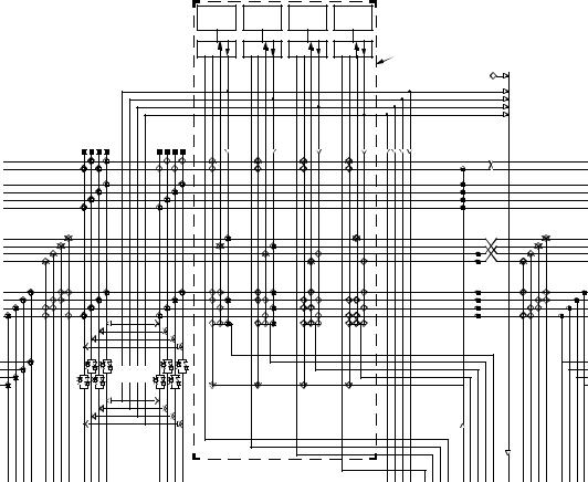
|
Data Sheet |
ORCA Series 2 FPGAs |
June 1999 |
|
|
Programmable Input/Output Cells (continued)
|
|
|
|
|
|
|
|
|
|
|
|
|
|
|
|
|
|
|
|
PA |
|
|
PB |
|
|
|
PC |
|
|
|
PD |
|
|
|
|
|
|
|
|
|
|
|
|
|
|
|
|
|
|
|
|
|
|
|
|
|
|
|
|
|
|
|
|
|
|
|
|
|
|
|
D T |
|
D T |
|
D T |
|
D T |
|
|
PIC DETAIL |
|
|
|
|
|
|
|
|
|
|
|
|
|
|
|
||||||||||
|
|
|
|
|
|
|
|
|
|
|
|
|
|
|
|
|
|
|
|
|
|
|
|
|
|
|
|
|
|
|
|
|
|
|
|
|
|
|
|
|
|
|
|
|
|
|
|
|
||||
|
|
|
|
|
|
|
|
|
|
|
|
|
|
|
|
|
|
DOUT0 |
TS0 |
OUT0 |
IN0 |
DOUT1 TS1 |
OUT1 |
IN1 |
DOUT2 |
TS2 |
OUT2 |
IN2 |
DOUT3 |
TS3 |
OUT3 |
IN3 |
|
|
|
|
|
|
|
|
|
|
|
|
|
|
|
|
|
|
|
|
|
|
|
|
|
|
|
|
|
|
|
|
|
|
|
|
|
|
|
|
|
|
|
|
|
|
|
|
|
|
|
|
F |
|
|
|
|
|
|
|
|
|
|
|
|
Q |
|
|
|
|
|
|
|
|
|
|
|
|
|
|
|
|
K BIDIH3 |
BIDIH2 |
BIDIH1 |
BIDIH0 |
|
BIDI3 |
BIDI2 |
BIDI1 |
BIDI0 |
J |
|
|
|
|
|
|
|
|
|
|
|
|
|
|
|
|
|
|
|
|
|
|
|
|
|
|
|
|
|
|
|
|
|
|
|
PXL[1] |
|
|
|
|
|
|
|
|
|
|
|
|
|
|
|
|
|
|
|
|
|
|
|
|
|
|
|
|
|
|
|
|
|
|
|
|
|
|
|
|
|
|
|
|
|
|
|
|
|
|
PXL[0] |
A PXL[0] |
|
|
|
|
|
|
|
|
|
|
|
|
|
|
|
|
|
|
|
|
|
|
|
|
|
|
|
|
|
|
|
|
|
|
|
|
|
|
|
|
|
|
|
|
|
|
|
|
|
|
PXL[1] A |
|
|
PXH[0] |
|
|
|
|
|
|
|
|
|
|
|
|
|
|
|
|
|
|
|
|
|
|
|
|
|
|
|
|
|
|
|
|
|
|
|
|
|
|
|
|
|
|
|
|
|
|
|
|
|
|
PXH[0] |
|
PXH[1] |
|
|
|
|
|
|
|
|
|
|
|
|
|
|
|
|
|
|
|
|
|
|
|
|
|
|
|
|
|
|
|
|
|
|
|
|
|
|
|
|
|
|
|
|
|
|
|
|
|
|
PXH[1] |
B PXH[2] |
|
|
|
|
|
|
|
|
|
|
|
|
|
|
|
|
|
|
|
|
|
|
|
|
|
|
|
|
|
|
|
|
|
|
|
|
|
|
|
|
|
|
|
|
|
|
|
|
|
|
PXH[2]B |
|
|
PXH[3] |
|
|
|
|
|
|
|
|
|
|
|
|
|
|
|
|
|
|
|
|
|
|
|
|
|
|
|
|
|
|
|
|
|
|
|
|
|
|
P |
|
|
|
|
|
|
|
|
|
|
|
PXH[3] |
|
|
|
|
|
|
|
|
|
|
|
|
|
|
|
|
|
|
|
|
|
|
|
|
|
|
|
|
|
|
|
|
|
|
|
|
|
|
|
|
|
|
|
|
|
|
|
|
|
|
|
|
|
|
PX2[2] |
|
|
|
|
|
|
|
|
|
|
|
|
|
|
|
|
|
|
|
|
|
|
|
|
|
|
|
|
|
|
|
|
|
|
|
|
|
|
|
|
|
|
|
|
|
|
|
|
|
|
PX2[0] |
C |
PX2[3] |
|
|
|
|
|
|
|
|
|
|
|
|
|
|
|
|
|
|
|
|
|
|
|
|
|
|
|
|
|
|
|
|
|
|
|
|
|
|
|
|
|
|
|
|
|
|
|
|
|
|
PX2[1] |
PX2[0] |
|
|
|
|
|
|
|
|
|
|
|
|
|
|
|
|
|
|
|
|
|
|
|
|
|
|
|
|
|
|
|
|
|
|
|
|
|
|
|
|
|
|
|
|
|
|
|
|
|
|
PX2[2] C |
|
|
PX2[1] |
|
|
|
|
|
|
|
|
|
|
|
|
|
|
|
|
|
|
|
|
|
|
|
|
|
|
|
|
|
|
|
|
|
|
|
|
|
|
|
|
|
|
|
|
|
|
|
|
|
|
PX2[3] |
|
|
|
|
|
|
|
|
|
|
|
|
|
|
|
|
|
|
|
|
|
|
|
|
|
|
|
|
|
|
|
|
|
|
|
|
|
|
|
|
|
C |
|
|
|
|
|
|
|
|
|
|
|
|
PX1[0] |
|
|
|
M |
|
|
|
|
|
|
|
|
|
|
|
|
|
|
|
|
|
|
|
|
|
|
|
|
|
|
|
|
|
|
|
|
|
|
|
|
|
|
|
|
|
|
|
M |
|
|
PX1[0] |
|
|
|
|
|
|
|
|
|
|
|
|
|
|
|
|
|
|
|
|
|
|
|
|
|
|
|
|
|
|
|
|
|
|
|
|
|
|
|
|
|
|
|
|
|
|
|
|
|
|
|
||
|
PX1[1] |
|
|
|
|
|
|
|
|
|
|
|
|
|
|
|
|
|
|
|
|
|
|
|
|
|
|
|
|
|
|
|
|
|
|
|
|
|
|
|
|
|
|
|
|
|
|
|
|
|
|
PX1[1] |
D PX1[2] |
|
|
|
|
|
|
|
|
|
|
|
|
|
|
|
|
|
|
|
|
|
|
|
|
|
|
|
|
|
|
|
|
|
|
|
|
|
|
|
|
|
|
|
|
|
|
|
|
|
|
PX1[2] D |
|
|
PX1[3] |
|
|
|
N |
|
|
|
|
|
|
|
|
|
|
|
|
|
|
|
|
|
|
|
|
|
|
|
|
|
|
|
|
|
|
|
|
|
|
|
|
|
|
|
|
|
|
|
|
|
|
PX1[3] |
|
|
|
|
|
|
|
|
|
|
|
|
|
|
|
|
|
|
|
|
|
|
|
|
|
|
|
|
|
|
|
|
|
|
|
|
|
|
|
|
D |
|
|
|
|
|
|
|
|
|
|
N |
|
|
|
|
|
|
|
|
|
|
|
|
|
|
|
|
|
|
|
|
|
|
|
|
|
|
|
|
|
|
|
|
|
|
|
|
|
|
|
|
|
|
|
|
|
|
|
|
|
|
|
|
||
|
|
|
|
|
|
|
|
|
|
|
|
|
|
|
|
|
|
|
|
|
|
|
|
|
|
|
|
|
|
|
|
|
|
|
|
|
|
|
|
|
|
|
|
|
|
|
|
|
|
|
|
|
|
|
|
|
|
O |
|
|
|
I |
|
|
LLIN3 |
LLIN2 LLIN1 |
LLIN0 |
|
|
|
|
|
|
|
|
|
|
|
|
|
|
|
|
|
|
|
|
|
|
|
|
|
|
|
|
|
|
|
|
|
|
|
|
|
O |
|
|
|
|
|
|
|
|
|
|
|
|
|
|
|
|
|
|
|
|
|
|
|
|
|
|
|
|
|
|
|
|
|
|
|
|
|
|
|
|
|
|
|
|
|
|
|
|
|
||||
|
|
|
|
|
|
|
|
|
|
|
|
|
|
|
|
|
|
|
|
|
|
|
|
|
|
|
|
|
|
|
|
|
|
|
|
|
|
|
|
|
|
|
|
|
|
|
|
|
|
|
|
|
|
|
|
|
|
|
|
|
|
|
|
|
|
|
|
|
|
|
|
|
|
|
|
|
|
|
|
|
P |
|
|
|
|
|
|
|
|
LLDRV |
|
|
|
|
|
|
|
|
|
|
|
|
|
|
|
|
|
|
|
|
|
|
|
|
|
|
|
|
|
|
|
|
|
|
|
|
|
|
|
|
|
|
|
|
|
|
|
|
|
|
|
|
P |
|
|
|
|
|
|
|
|
|
|
|
|
|
|
|
|
|
|
|
|
|
|
|
|
|
|
|
|
L |
|
|
|
|
|
|
|
|
|
|
|
|
|
|
|
|
|
|
|
|
|
|
|
|
|
|
|
|
|
|
|
|
|
|
|
|
|
|
|
|
|
|
|
|
|
|
|
|
|
|
|
|
|
|
|
|
|
|
|
|
|
|
|
|
|
|
|
|
|
|
|
|
|
|
|
|
|
|
|
|
|
|
|
|
Q |
|
|
|
|
|
|
|
|
VX4[7] |
VX4[6] |
VX4[5] |
VX4[4] |
VX1[7] |
VX1[6] |
VX1[5] |
VX1[4] |
VXH[3] |
VXH[2] |
VXH[1] |
VXH[0] |
|
VXL[3] |
VXL[2] |
VXL[1] |
VXL[0] |
|
|
|
|
|
|
|
|
|
|
|
|
|
|
PDINTB[3] |
PDINTB[2] |
PDINTB[1] |
PDINTB[0] |
DOUT[3] |
DOUT[2] DOUT[1] |
DOUT[0] |
XSW[4] |
XSW[3] |
XSW[2] |
XSW[1] |
XSW[0] |
CKT |
VX1[3] |
VX1[2] |
VX1[1] |
VX1[0] |
VX4[3] |
VX4[2] |
VX4[1] |
VX4[0] |
|
|
|
|
|
|
|
|
|
|
|
|
|
|
|
|
|
|
|
|
|
|
|
|
|
|
|
|
|
|
|
|
|
|
F |
|
|
E |
|
|
|
G |
|
|
|
|
|
|
|
|
|
|
|
|
|
|
|
|
|
|
|
|
|
|
|
|
|
|
|
|
|
|
|
|
|
|
|
|
|
|
|
|
|
|
|
|
|
|
|
|
|
|
|
|
|
|
|
|
|
|
|
|
|
|
|
5-2843(F).r8 |
Figure 26. PIC Architecture
PLC-PIC Routing Resources
There is no direct connection between the inter-PIC lines and the PLC lines. All connections to/from the PLC must be done through the connecting lines which are perpendicular to the lines in the PIC. The use of perpendicular and parallel lines will be clearer if the PLC and PIC architectures (Figure 23 and Figure 26) are placed side by side. Twenty-nine lines in the PLC can be connected to the 15 lines in the PIC.
Multiple connections between the PIC PX1 lines and the PLC X1 lines are available. These allow buses placed in any arbitrary order on the I/O pads to be unscrambled when placed on the PLC X1 lines. Con-
nections are also available between the PIC PX2 lines and the PLC X1 lines.
There are eight tridirectional (four TRIDI/four TRIDIH) buffers in each PIC; they can do the following:
■Drive a signal from an I/O pad onto one of the adjacent PLC’s XL or XH lines
■Drive a signal from an I/O pad onto one of the two PXL or four PXH lines in the PIC
■Drive a signal from the PLC XL or XH lines onto one of the two PXL or four PXH lines in the PIC
■Drive a signal from the PIC PXL or PXH lines onto one of the PLC XL or XH lines
30 |
Lucent Technologies Inc. |
 Loading...