

AGERE D1861D040, D1861D023, D1861D050 Datasheet
Preliminary Data Sheet
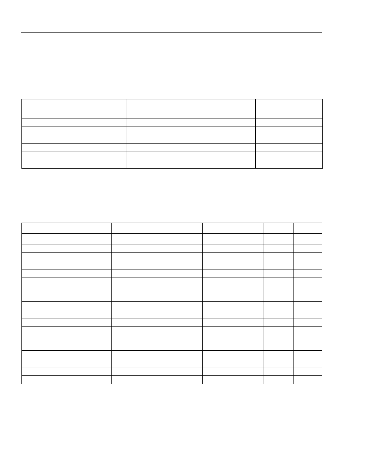
ESD
PROTECTION
TEC
7654 321
–––++
RF
R
MATCH
45
Ω
R
TH
10 kΩ @ 25 °C
ISOLATOR
RF CONNECTOR
MPD
DFB
CHOKE
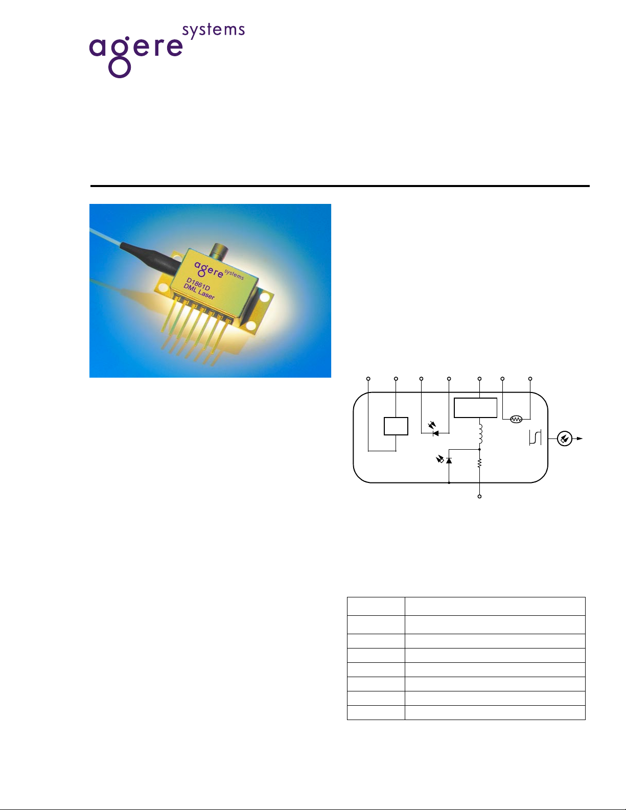
D1861D 10 Gbits/s 1310 nm DML Module (10 dBm)
Description
The D1861D direct-modulated laser (DML) module is
a cost-effective solution for 10 Gbits/s digital transmission up to 50 km using traditional intracity
SMF-28
wavelength eliminates the need for concern about
dispersion control over most installed intracity fiber
plants. The package contains a high-speed DFB
laser chip, thermoelectric cooler, thermistor, optical
isolator, and a rear-facet monitor photodiode, which
allows for external optical power control.
†
single-mode fiber links. The 1310 nm
March 2001
Features
■
Direct-modulated 1310 nm laser module characterized for use in 10 Gbits/s operations up to 50 km
■
High package slope efficiency
■
Av erage optical output power capability, 10 dBm
■
Temperature stabilized with internal thermoelectric
cooler (TEC), enabling operation within a wide
temperature range of –5 °C to +80 °C
■
Hermetically sealed optics, isolator on TEC
■
GPO*
RF connector
■
Single-mode fiber pigtail
■
High relaxation frequency at low bias
Applications
■
SONET/SDH low-cost metro applications
■
High-speed data communications
■
DWDM equipment drop-side applications
*
GPO
is a trademark of Gilbert Engineering Co., Inc.
Figure 1. D1861D DML Electrical Schematic
Pin Information
Table 1. Pin Descriptions
Pin No. Description
1Thermistor
2Thermistor
3 Laser Cathode (–), dc Bias
4 MPD Anode, (Negative Bias MPD)
5 MPD Cathode
6 Thermoelectric Cooler (+)
7 Thermoelectric Cooler (–)
1. Laser anode is case ground mAp-p drive current.
2. A positive current into this pin cools the laser.
†
SMF-28
is a trademark of Corning Incorporated.
1-1157(F)
1
2
Preliminary Data Sheet
D1861A 10 Gbits/s 1310 nm DML Module (10 dBm) March 2001
Absolute Maximum Ratings
Stresses in excess of the absolute maximum ratings can cause permanent damage to the device. These are absolute stress ratings only. Functional operation of the device is not implied at these or any other conditions in excess
of those given in the operational sections of the data sheet. Exposure to absolute maximum ratings for extended
periods can adversely affect device reliability. RF input shall be ac coupled. It is recommended that a series inductor of 100
Operating Temperature Range T
Storage Case Temperature Range Tstg — –40 85
Laser Forward Bias — TEC On — 150 mA
Pin 3, Max Positive Voltage
Pin 3, Max Positive Current
Reverse Voltage Photodiode V
TEC Current I
1. RF connector ac coupled.
µ
H be placed external to the device on Pin 3.
Parameter Symbol Condition Min Max Unit
OP
1
1
V
R
I
R
RPD
TEC
— –40 80
——1V
— — 200 mA
——20V
——1.7A
°
C
°
C
Electrical/Optical Characteristics
Table 2. Electrical and Optical Characteristics
Parameter S ymbol Condition Min Typ Max Unit
Average Optical Output Power P
Threshold Current (BOL) I
Wavelength
Wavelength Tuning Coefficient
External Efficiency
∆λ
O
TH
λ
T
η
ac Side-mode Suppression Ratio SMSR I
Chromatic Dispersion Penalty
——
(50 km, SMF28, 200 ps/nm)
Optical Isolation — — 32 — — dB
High-frequency Cutoff (3 dB) F
Low-frequency Cutoff (3 dB) F
RF Return Loss, 50 Ω
HIGH
LOW
IS
II
11
(0.1 GHz—8 GHz)
Rise/Fall Time, 10%—90% t
Thermoelectric Cooler Current I
Thermistor Resistance R
R/tF
TEC
TH
Thermistor Coef fic ient — — — –4.4 — %/°C
Monitor Photodiode Current I
1. 10 Gbits/s PRBS 223–1, ER = 8.2 dB, @ IOP, TOP = 25 °C, typical 50 mAp–p drive current.
2. Measurements made with 100 µH in series with pin 3 (laser cathode).
MPD
(Case temperature, –5 °C to +80 °C; laser temperature, 25 °C
unless otherwise noted.)
≈
I
ITH + 30 mA 7 — — mW
OP
—2—30mA
— 1290 — 1320 nm
— — 0.085 — nm/°C
—0.24——W/A
35 — — dB
——1.0dB
14 — — GHz
——30kHz
10 — — dB
— — 50 ps
I
I
OP
OP
OP
OP
—
1
2
2
1
———1.3A
— 9.5 10 10.5 k
I
OP
40 — 1500
µ
Ω
A
2
Agere Systems Inc.
 Loading...