

Preliminary Data Sheet
ESD
PROTECTION
TEC
7654 321
–––++
RF
R
MATCH
45
Ω
R
TH
10 kΩ @ 25 °C
ISOLATOR
RF CONNECTOR
MPD
DFB
CHOKE
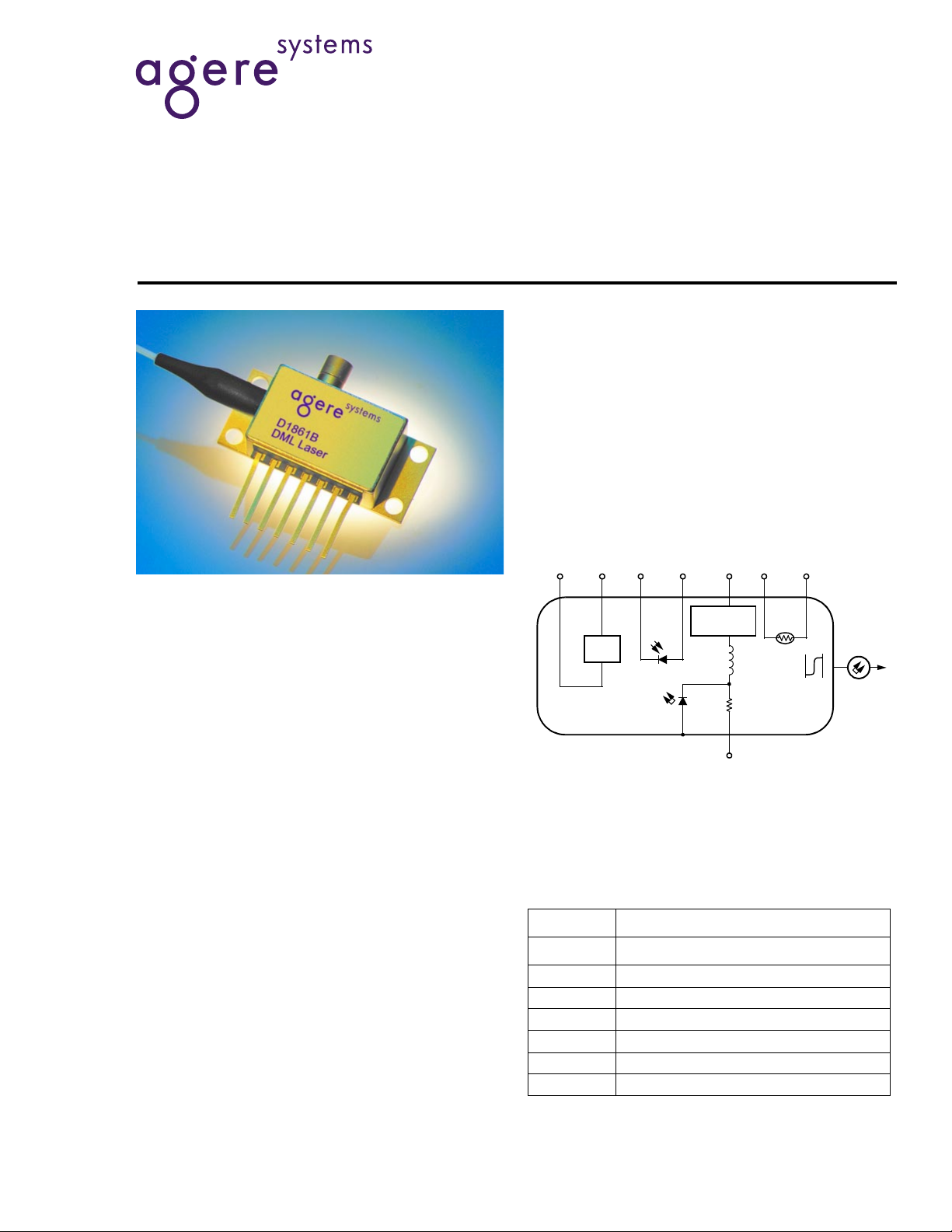
D1861B 10 Gbits/s 1310 nm DML Module (–3 dBm)
Description
The D1861B direct-modulated laser (DML) module is
a cost-effective solution for 10 Gbits/s digital transmission up to 12 km using traditional intracity
SMF-28
wavelength eliminates the need for concern about
dispersion control over most installed intracity fiber
plants. The package contains a high-speed DFB
laser chip, thermoelectric cooler, thermistor, optical
isolator, and a rear-facet monitor photodiode, which
allows for external optical power control.
†
single-mode fiber links. The 1310 nm
March 2001
Features
■
Direct-modulated 1310 nm laser module characterized for use in 10 Gbits/s operations up to 12 km
■
Av erage optical output power, –3 dBm typical
■
Temperature stabilized with internal thermoelectric
cooler (TEC), enabling operation within a wide
temperature range of –5 °C to +80 °C
■
Hermetically sealed optics, isolator on TEC
■
GPO*
RF connector
■
Single-mode fiber pigtail
■
High relaxation frequency at low bias
Applications
■
SR-1
■
SONET/SDH low-cost metro applications
■
High-speed data communications
■
DWDM equipment drop-side applications
*
GPO
is a trademark of Gilbert Engineering Co., Inc.
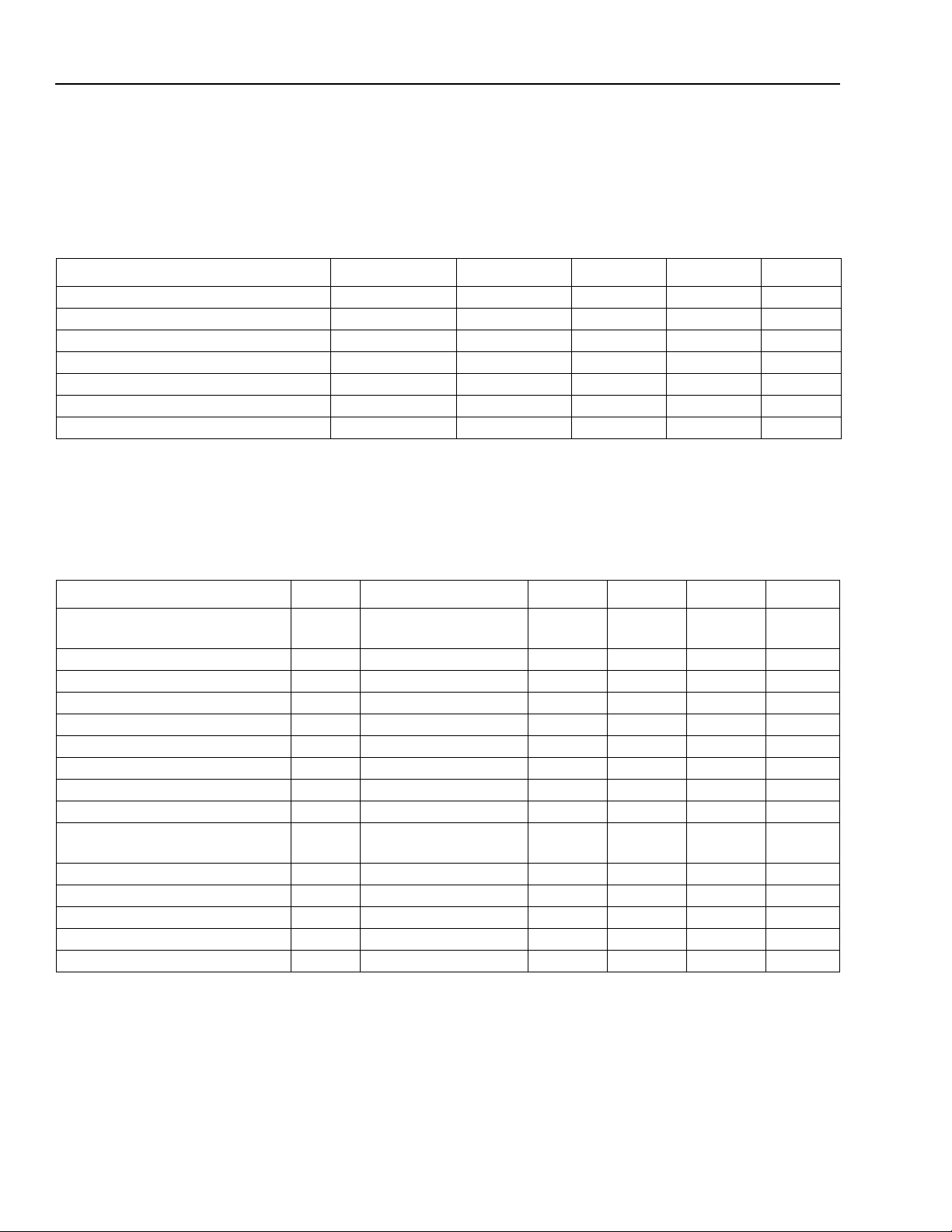
Figure 1. D1861B DML Electrical Schematic
Pin Information
Table 1. Pin Descriptions
Pin No. Description
1Thermistor
2Thermistor
3 Laser Cathode (–), dc Bias
4 MPD Anode, (Negative Bias MPD)
5 MPD Cathode
6 Thermoelectric Cooler (+)
7 Thermoelectric Cooler (–)
1. Laser anode is case ground mAp-p drive current.
2. A positive current into this pin cools the laser.
†
SMF-28
is a trademark of Corning Incorporated.
1-1157(F)
1
2
Preliminary Data Sheet
D1861B 10 Gbits/s 1310 nm DML Module (–3 dBm) March 2001
Absolute Maximum Ratings
Stresses in excess of the absolute maximum ratings can cause permanent damage to the device. These are absolute stress ratings only. Functional operation of the device is not implied at these or any other conditions in excess
of those given in the operational sections of the data sheet. Exposure to absolute maximum ratings for extended
periods can adversely affect device reliability. RF input shall be ac coupled. It is recommended that a series inductor of 100
Operating Temperature Range T
Storage Case Temperature Range Tstg — –40 85
Laser Forward Bias — TEC On — 150 mA
Pin 3, Max Positive Voltage
Pin 3, Max Positive Current
Reverse Voltage Photodiode V
TEC Current I
1. RF connector ac coupled.
µ
H be placed external to the device on Pin 3.
Parameter Symbol Condition Min Max Unit
OP
1
1
V
R
I
R
RPD
TEC
— –40 80
——1V
— — 200 mA
——20V
——1.7A
°
C
°
C
Electrical/Optical Characteristics
Table 2. Electrical and Optical Characteristics
Parameter S ymbol Condition Min Typ Max Unit
Average Optical Output Power P
Threshold Current (BOL) I
Wavelength
Wavelength Tuning Coefficient
External Efficiency
∆λ
O
TH
λ
T
η
ac Side-mode Suppression Ratio SMSR I
Optical Isolation — — 32 — — dB
High-frequency Cutoff (3 dB) F
Low-frequency Cutoff (3 dB) F
RF Return Loss, 50 Ω
HIGH
LOW
IS
II
11
(0.1 GHz—8 GHz)
Rise/Fall Time, 10%—90% t
Thermoelectric Cooler Current I
Thermistor Resistance R
R/tF
TEC
TH
Thermistor Coef fic ient — — — –4.4 — %/°C
Monitor Photodiode Current I
1. 10 Gbits/s PRBS 223–1, ER = 8.2 dB, @ IOP, TOP = 25 °C, typical 50 mAp–p drive current.
2. Measurements made with 100 µH in series with pin 3 (laser cathode).
MPD
(Case temperature, –5 °C to +80 °C; laser temperature, 25 °C
unless otherwise noted.)
I
OP = ITH
+ 30 mA –5.5
0.28
—
—
–1.5
0.71
dBm
—2—30mA
— 1290 — 1320 nm
— — 0.085 — nm/°C
—9.4—23.8mW/A
35 — — dB
14 — — GHz
——30kHz
10 — — dB
— — 50 ps
I
I
OP
OP
OP
OP
—
2
2
1
———1.3A
— 9.5 10 10.5 k
I
OP
40 — 1500
mW
µ
Ω
A
2
Agere Systems Inc.

Preliminary Data Sheet
March 2001 D1861B 10 Gbits/s 1310 nm DML Module (–3 dBm)
Characteristic Curve
Figure 2. Filtered Optical Eye Pattern (0 km, Fourth
Order Bessel Filter, 8.2 dB ER, 20 ps/div)
Outline Diagram
Dimensions are in inches and (millimeters).
RF INPUT
LIMITED DETENT
GPO OR SMP
CONNECTOR
0.164 DIA
* HYTREL
0.365
(9.45
9.09)
0.040
(1.19
0.84)
0.248
(6.45
6.12)
0.228
(5.97
5.61)
1.025
(26.21
25.86)
0.420
(10.85
10.49)
FIBER AND BEND LIMITER
MAINTAIN FIBER BEND RADIUS
GREATER THAN 1.5”
0.318
(8.26
7.90)
0.190
(5.00
4.65)
0.105 DIA
4 PLCS
0.250
(6.53
6.17)
is a trademark of E. I. du Pont de Nemours and Company.
0.350
(9.07
8.71)
0.078
(2.16
1.80)
LEADS
0.008” THICK x 0.030” WIDE
0.400” MIN. LENGTH
6 SPCS @ 0.100” (0.254)
PIN 1
0.212
(5.56
0.9 mm
0.500
(12.88
0.048
(1.40
1.04)
5.21)
HYTREL*
TIGHT-BUFFERED JACKET
0.215 ± 0.010
(5.50 ±0.30)
0.600
(15.00)
∅
OVER ACRYLATE-COATED FIBER
12.52)
0.820
(20.80)
1.180
(30.00)
1-1156(F)
Agere Systems Inc.
3

Preliminary Data Sheet
D1861B 10 Gbits/s 1310 nm DML Module (–3 dBm) March 2001
Laser Safety Information
Class IIIb Laser Product
FDA/CDRH Class IIIb laser product. All versions are Class IIIb laser products per CDRH, 21 CFR 1040 Laser
Safety requirements. All versions are Class 3B laser products per
fied with the FDA under an accession number to be determined.
This product complies with 21 CFR 1040.10 and 1040.11.
SMF28 single-mode fiber pigtail and connector
Wavelength = 1.3 µm
Maximum power = 30 mW
Because of size constraints, laser safety labeling (including an FDA Class IIIb label) is not affixed to the module but
attached to the outside of the shipping carton.
Product is not shipped with power supply.
Caution: Use of controls, adjustments, and procedures other than those specified herein may result in
hazardous laser radiation exposure.
IEC
* 60825-1:1993. The device has been classi-
DANGER
INVISIBLE LASER RADIATION
IS EMITTED FROM THE END
OF FIBER OR CONNECTOR
Avoid direct exposure to beam
Do not view beam directly with
optical instruments
INVISIBLE LASER RADIATION EMITTED FROM END OF FIBER OR CONNECTOR
Avoid exposure to beam
Class 3B Laser Product IEC-60825M 1993 Max. Output: 30 mW Wavelength: 1.3 µm
*
IEC
is a registered trademark of The International Electrotechnical Commission.
4
Agere Systems Inc.

Preliminary Data Sheet
March 2001 D1861B 10 Gbits/s 1310 nm DML Module (–3 dBm)
Ordering Information
Table 3. Ordering Information1
Device Code Description Connector Pigtail Comcode
D1861B023 10 Gbits/s DML,
1310 nm
D1861B040 10 Gbits/s DML,
1310 nm
D1861B050 10 Gbits/s DML,
1310 nm
1. Other options available. For additional ordering information, please contact an account manager at Opto West, Agere Systems Inc., 1-800362-3891 (for sales staff, please p ress option 2).
FC/SPC
SC/UPC
Standard
LC
SMF-28
SMF-28
SMF-28
(1 m min) TBD
(1 m min) TBD
(1 m min) TBD
Agere Systems Inc.
5

Preliminary Data Sheet
D1861B 10 Gbits/s 1310 nm DML Module (–3 dBm) March 2001
For additional information, contact your Agere Systems Account Ma na ger or the following:
INTERNET: http://www.agere.com
E-MAIL: docmaster@micro.lucent.com
N. AMERICA: Agere Systems Inc., 555 Union Boulevard, Room 30L-15P-BA, Allentown, PA 18109-3286
ASIA PACIFIC: Agere Systems Singapore Pte. Ltd., 77 Science Park Drive, #03-18 Cintech III, Singapore 118256
CHINA: Agere Systems (Shanghai) Co., Ltd., 33/F Jin Mao Tower, 88 Century Boulevard Pudong, Shanghai 200121 PRC
JAPAN: Agere Systems Japan Ltd., 7-18, Higashi-Gotanda 2-chome, Shinagawa-ku, Tokyo 141, Japan
EUROPE: Data Requests: DATALINE: Tel. (44) 7000 582 368, FAX (44) 1189 328 148
Agere Systems Inc. reserves the right to make changes to the product(s) or information contained herein without notice. No liability is assumed as a result of their use or application.
Copyright © 2001 Agere Systems Inc.
All Rights Reserved
March 2001
DS01-125OPTO
1-800-372-2447, FAX 610-71 2-4106 (In CANADA: 1-800-553-2448, FAX 610-712-4106)
Tel. (65) 778 8833, FA X (65) 777 7495
Tel. (86) 21 50471212, FAX (86) 21 50472266
Tel. (81) 3 5421 1600, FAX (81) 3 5421 1700
Technical Inquiries: OPTOELECTRONICS MARKETING: (44) 1344 865 900 (Ascot UK)
 Loading...