


Data Sheet
December 1999
CSP1027 Voice Band Codec for
Cellular Handset and Modem Applications
1 Features
∆-Σ (delta-sigma) A/D and D/A converters with stan-
■
dard 16-bit serial I/O interface.
■ On-chip filters meet ITU-T G.712 voice band fre-
quency response and signal to distortion plus noise
specifications. Suitable for IS-54, GSM, and JDC digital cellular applications.
■ Low-profile package (<1.5 mm) 48-pin thin quad flat
pack (TQFP) available or 44-pin EIAJ quad flat pack
(QFP).
■ Operates in systems with a 3.0 V to 5.0 V digital
power supply and a 5.0 V analog supply.
■ Low-power 0.9 µm CMOS technology, fully static
design, typical power of 68 mW when active and
0.05 mW in standby with a 3.3 V digital supply and a
5.0 V analog supply.
■ A low-power inactive (standby) state without stopping
clock or removing power supply.
■ Sampling rates up to 24 kHz.
■ On-chip programmable sampling clock generator
allows input clock to be an integer multiple of
125 times the sampling rate or an integer multiple of
the sampling rate.
■ Programmable phase adjust of both codec sampling
clock and baseband codec clock.
■ Two on-chip clock dividers for generating the output
clock for the baseband codec and the output clock
for other processors.
■ Regulated microphone power supply.
■ Microphone preamplifier, with programmable input
ranges of 0.16 Vp and 0.5 Vp.
■ Output amplifier, with programmable gain settings,
0 dB to –45 dB in –3 dB steps.
■ High-pass filters selectable via control registers.
■ Power-on reset pulse generator.
■ Standard 16-bit serial I/O interface.
■ Serial I/O multiprocessor mode compatible with the
Lucent Technologies Microelectronics Group’s
DSP16A and DSP1610/1616/1617/1618 Digital Signal Processors.
2 Description
The Lucent CSP1027 is a high-precision linear voiceband ∆-Σ (delta-sigma) codec designed for cellular
handset and modem applications. The device is fabricated in low-power CMOS technology and designed for
low-voltage (3.0 V to 5.0 V) digital systems. The
CSP1027 is packaged in a 44-pin EIAJ quad flat pack
(QFP) or a 48-pin EIAJ thin quad flat pack (TQFP). In
the 48-pin TQFP, the CSP1027 occupies a total volume
of 0.0784 cm
The CSP1027 has a variety of significant programmable features not found in standard voice band codecs.
The analog interface includes a microphone preamplifier with programmable gain settings, an output amplifier with gain programmable in 3 dB steps over a 45 dB
range, and a regulated microphone power supply. An
inactive mode allows a low-power standby state, and a
mute function provides suppression of the analog output. On-chip antialiasing and anti-imaging filtering
includes a selectable high-pass filter. The CSP1027
meets ITU-T G.712 voice band specifications.
The programmable features of the CSP1027 are set by
writing four on-chip control registers through the serial
I/O interface. The codec’s digital input/output uses a
linear 16-bit two’s complement data format that is also
transferred through the serial I/O interface. The
CSP1027 interfaces easily to the 16-bit serial ports of
digital signal processors and other devices. The serial
interface supports the Lucent fixed-point DSP family
serial multiprocessor mode. This allows up to eight
compatible devices, including two CSP1027s, to interface to each other on a common 4-wire bus using a
time-division-multiplexing scheme.
3
.

CSP1027 Voice Band Codec for Data Sheet
Cellular Handset and Modem Applications December 1999
Table of Contents
Contents Page
1 Features........................................................................................................................................... ....... .... 1
2 Description...................................... ....... ...... ....... ...... ....... ............................................ . ...... ...... . ...... ....... .... 1
3 Pin Information ........................................................................................................................................... 3
4 Architectural Information ............................................................................................................................ 5
4.1 Overview............................... ....... ...... ....... ...... ....... ...... ....... ...... ............................................. ....... .... 6
4.2 Description of Signal Paths............................................................................................................... 6
4.3 Programmable Features................................................................................................................. 13
4.4 Power-On Reset............................................................................................................................. 14
4.5 Clock Generation............................................................................................................................ 16
4.6 Serial I/O Configurations................................................................................................................. 20
5 Register Information.................................................................................................................................. 26
5.1 Codec I/O Control 0 (
5.2 Codec I/O Control 1 (
5.3 Codec I/O Control 2 (
5.4 Codec I/O Control 3 (
6 Signal Descriptions ................................................................................................................................... 30
6.1 Clock Interface................................................................................................................................ 30
6.2 Reset Interface ............................................................................................................................... 31
6.3 Serial I/O Interface.......................................................................................................................... 31
6.4 External Gain Control Interface ...................................................................................................... 32
6.5 Digital Power and Ground......................................................... ...... ....... ...... ....... ...... ....... ............... 32
6.6 Analog Interface.............................................................................................................................. 32
6.7 Analog Power and Ground ............................................................................................................. 32
7 Application Information ............................................................................................................................. 33
7.1 Analog Information.......................................................................................................................... 33
7.2 Power Supply Configuration........................................................................................................... 36
7.3 The Need for Fully Synchronous Operation ................................................................................... 36
7.4 Crystal Oscillator............................................................................................................................. 38
7.5 Programmable Clock Generation ................................................................................................... 45
8 Device Characteristics .............................................................................................................................. 47
8.1 Absolute Maximum Ratings............................................................................................................ 47
8.2 Handling Precautions...... ...... ....... ...... ....... ...... ....... ............................................. ...... ....... ............... 47
8.3 Recommended Operating Conditi ons....................................... ...... ....... ...... ....... ...... ....... ...... ....... .. 47
9 Electrical Characteristics and Requirements ............................................................................................ 48
9.1 Power Dissipation........................................................................................................................... 50
10 Analog Characteristics and Requirements................................................................................................ 51
10.1 Analog Input and Microphone Regulator........................................................................................ 51
10.2 Analog-to-Digital Path........................ ....... ............................................. ...... ....... ...... ...................... 52
10.3 Digital-to-Analog Path........................ ....... ............................................. ...... ....... ...... ...................... 53
10.4 Miscellaneous................................................................................................................................. 54
11 Timing Characteristics and Requirements................................................................................................ 55
11.1 Clock Generation............................................................................................................................ 56
11.2 Power-On Reset............................................................................................................................. 57
11.3 Reset .............................................................................................................................................. 58
11.4 Serial I/O Communication .............................................................................................................. 59
11.5 Serial Multiprocessor Communication............................................................................................ 61
12 Outline Diagrams ...................................................................................................................................... 62
12.1 44-Pin EIAJ Quad Flat Pack (QFP)............................. ....... ...... ...... ....... ......................................... 62
12.2 48-Pin EIAJ Thin Quad Flat Pack (TQFP)...................................................................................... 63
cioc0
) Register....... ...... ....... ...... ....... ...... ...... ....... ......................................... 26
cioc1
) Register....... ...... ....... ...... ....... ...... ...... ....... ......................................... 27
cioc2
) Register....... ...... ....... ...... ....... ...... ...... ....... ......................................... 28
cioc3
) Register....... ...... ....... ...... ....... ...... ...... ....... ......................................... 29
2
Lucent Technologies Inc.
Data Sheet CSP1027 Voice Band Codec for
December 1999 Cellular Handset and Modem Applications
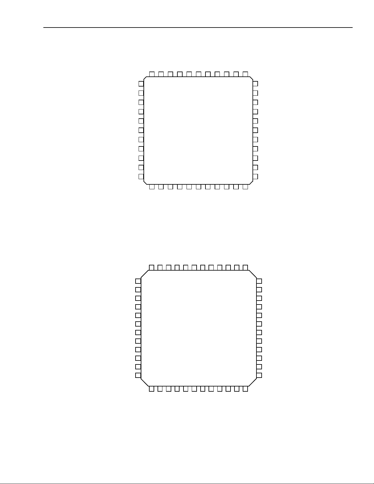
3 Pin Information
RES
RES
RES
SMODE1
SMODE0
RES
RES
RES
RES
RES
CKO1
1
2
3
4
5
6
7
8
9
10
11
DDA
V
44
12
CLK
AUXIN
43
13
XLO
REFC
42
14
XHI
SSA
MICIN
V
41
40
CPS1027-J
44-PIN QFP
15
16
CKO2
AOUTP
39
17
SS
V
RES
38
18
SADD
DDAVREGVSSA
AOUTN
V
37
36
19
20
DI
DO
35
21
DD
V
34
33
32
31
30
29
28
27
26
25
24
23
22
SYNC
EIGS
SMODE2
PORCAP
PORB
RSTB
RES
RES
RES
RES
RES
IOCK
XOSCEN
Figure 1. 44-Pin EIAJ Quad Flat Pack (QFP) Pin Diagram
5-7567 (F)
RES
RES
RES
SMODE1
SMODE0
RES
RES
RES
RES
RES
RES
CKO1 12
DDA
V
AUXIN
4847464544434241403938
1
2
3
4
5
6
7
8
9
10
11
REFC
MICIN
SSA
V
AOUTP
RES
CSP1027-S
48-PIN TQFP
AOUTN
DDAVREGVSSA
V
37 RES
EIGS
36
SMODE2
35
PORCAP
34
PORB
33
RSTB
32
RES
31
RES
30
RES
29
RES
28
RES
27
26
RES
25 IOCK
1314151617181920212223
CLK
XLO
XHI
SS
V
CKO2
SADD
DO
DD
V
RES
SYNC 24
DI
XOSCEN
Figure 2. 48-Pin EIAJ Thin Quad Flat Pack (TQFP) Pin Diagram
5-7568 (F)
Lucent T echnologies Inc.
3
CSP1027 Voice Band Codec for Data Sheet
Cellular Handset and Modem Applications December 1999
3 Pin Information
(continued)
Functional descriptions of the pins are found in Section 6 on page 30.
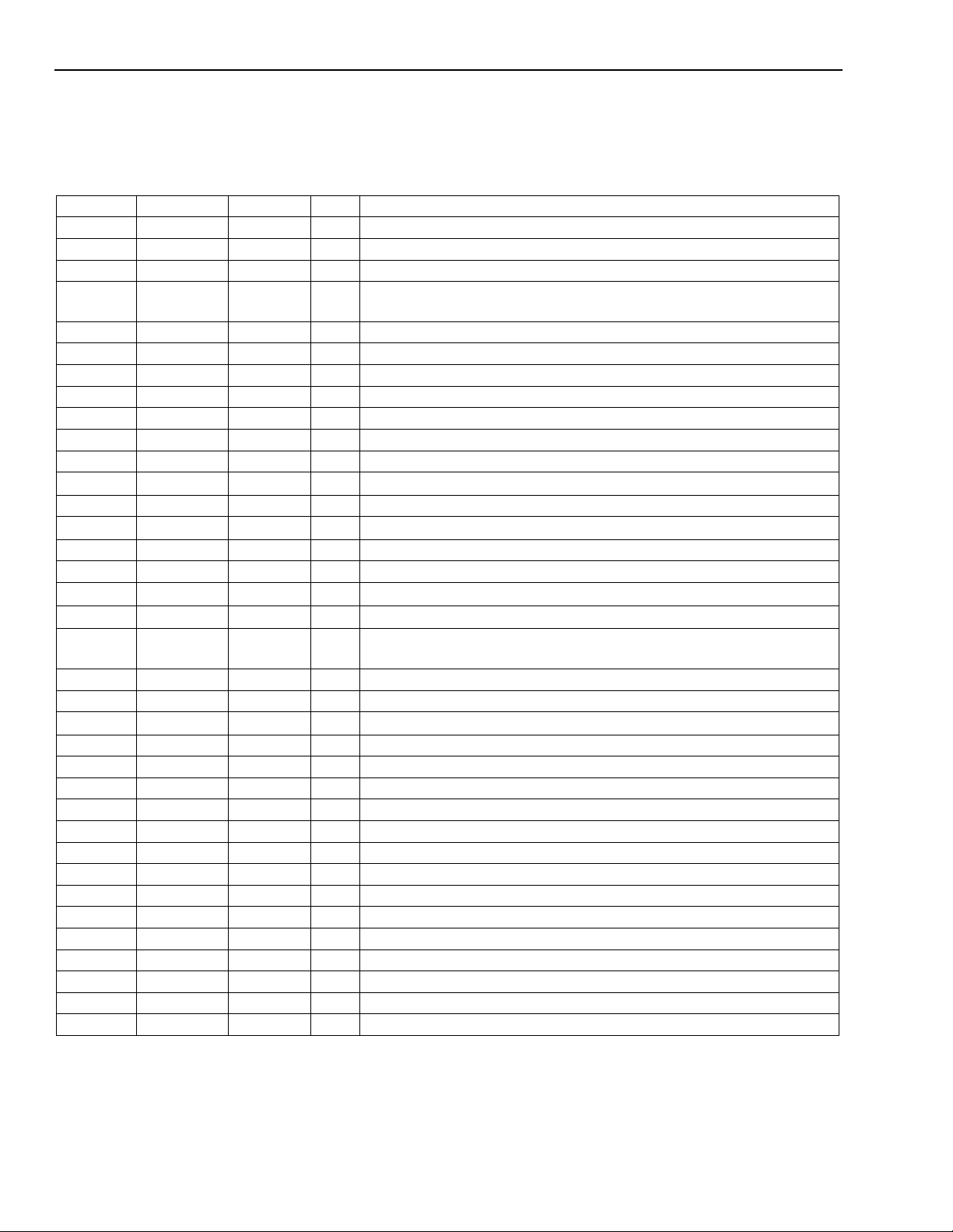
Table 1. Pin Descriptions
QFP Pin TQFP Pin Symbol Type Name/Function
1, 2, 3 1, 2, 3 RES NC* Reserved.
4 4 SMODE1 I Serial Mode Select 1.
5 5 SMODE0 I Serial Mode Select 0.
6, 7, 8,
9, 10
6, 7, 8,
9, 10, 11
RES NC* Reserved.
11 12 CKO1 O Clock Output 1.
12 13 CLK I Clock Input.
13 14 XLO I Crystal Input.
14 15 XHI O Crystal Output.
15 16 XOSCEN I Crystal Oscillator Enable.
16 17 CKO2 O Clock Output 2.
17 18 V
SS
18 19 SADD I/O
P Digital Ground.
†
Serial Address.
19 20 DI I Serial Input Data.
20 21 DO O
21 22 V
DD
†
Serial Output Data.
P Digital Power Supply.
— 23 RES NC* Reserved.
22 24 SYNC I/O
23 25 IOCK I
24, 25,
26, 27, 28
26, 27, 28,
29, 30, 31
RES NC* Reserved.
†
Serial Input/Output Load Strobe and Synchronization.
‡
Serial Clock.
29 32 RSTB I Reset.
30 33 PORB O Power-On Reset Output.
31 34 PORCAP I
§
External Capacitor Connection for Power-On Reset.
32 35 SMODE2 I Serial Mode Select 2.
33 36 EIGS I
**
External Input Gain Select.
— 37 RES NC* Reserved.
34 38 V
35 39 V
36 40 V
SSA
REG
DDA
P A nal og Ground.
A Regulated Output Voltage for Electrect Condenser Microphone.
P A nal og 5.0 V Power Supply.
37 41 AOUTN A Inverting Analog Output of Output Amplifier.
38 42 RES NC* Reserved.
39 43 AOUTP A Noninverting Analog Output of Output Amplifier.
40 44 V
SSA
P A nal og Ground.
41 45 MICIN A Analog Input for Microphone.
42 46 REFC A External Capacitor Connection for Internal Voltage Regulator.
43 47 AUXIN A Analog Input from Auxiliary.
44 48 V
* Indicates no connection.
† Indica tes 3-state output.
‡ Indica tes pull-up device on input.
§ Indicates pull-up resistor on input.
** Indicates pull-down device on input.
DDA
P A nal og 5.0 V Power Supply.
4
Lucent Technologies Inc.
Data Sheet CSP1027 Voice Band Codec for
December 1999 Cellular Handset and Modem Applications
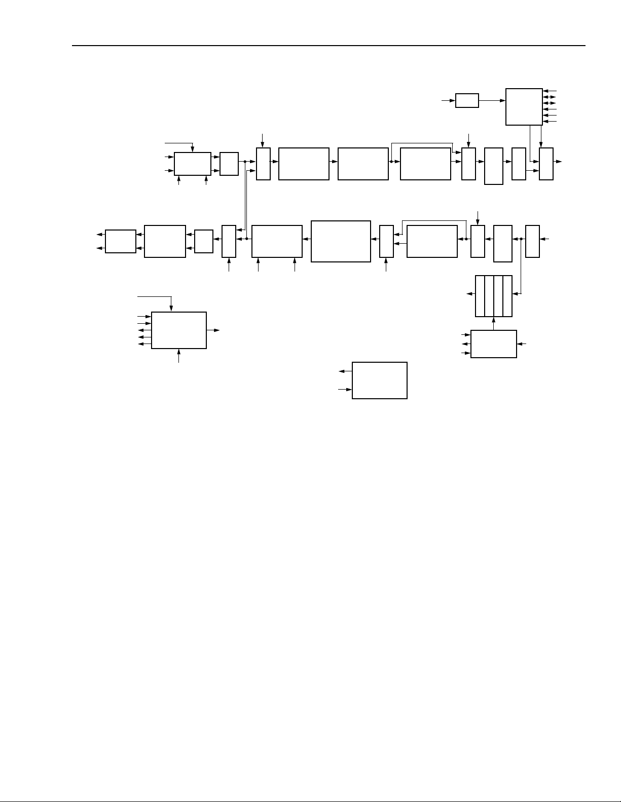
4 Architectural Information
AOUTP
AOUTN
EIGS
MIC
AUX
ANALOG
OUTPUT
AMP
XOSCEN
LOW-PASS
CLK
XLO
XHI
CKO1
CKO2
CDIV0 (cioc1), CDIV1 (cioc1),
CDIV2 (cioc0), CDIV3 (cioc2),
CDIF0 (cioc2), CDIF1 (cioc3),
CDIF2 (cioc3)
A/D INPUT
INSEL
cioc0
FILTER
(35 kHz)
CLOCK
GENERATION
BLOCK
TEST
cioc0
A/D
IRSEL
cioc0
M
U
D/A
X
TEST
DITHER
cioc0
cioc3
1 MHz OVERSAMPLING CLOCK
SYNC-CUBIC
M
U
DECIMATION
X
DIGITAL
MODULATOR
AND GAIN
ADJUST
OGSEL
cioc0
DIGITAL
FILTER
7th-ORDER
LOW-PASS
FILTER
SAMPLE/HOLD
AND 7th-ORDER
IIR
LOW-PASS
FILTER
V
REG
(3.0 V)
REFC
IIR
M
U
X
HPFE
cioc3
ON-CHIP
VOLTAGE
REFERENCE
CIRCUITS
3rd-ORDER
IIR
HIGH-PASS
FILTER
3rd-ORDER
IIR
HIGH-PASS
FILTER
PORCAP
PORB
RSTB
1/1251 MHz OVERSAMPLING CLOCK
HPFE
cioc3
M
U
X
8 kHz
(A/D)
MUTE
cioc0
M
U
T
E
c
c
i
o
o
c
c
3
2
POWER-ON
RESET
SIO
CONTROL
STATUS
C
O
D
S
X
R
C
D
X
(A/D)
c
c
i
i
i
o
o
c
c
1
0
INTERNAL RESET
M
U
X
I
S
R
TSTPOR
cioc3
IOCK
SYNC
SADD
SMODE2
SMODE1
SMODE0
DO
DI
5-7559 (F)
Figure 3. CSP1027 Block Diagram
Lucent T echnologies Inc.
5

CSP1027 Voice Band Codec for Data Sheet
Hz
()
1
25
------
1z
25
–
–
()
1z
1
–
–
()
-------------------------
×
3
=
Cellular Handset and Modem Applications December 1999
4 Architectural Information
(continued)
4.1 Overview
The CSP1027 is a complete analog-to-digital and digital-to-analog acquisition and conversion system (see
Figure 3 on page 5) that band limits and encodes analog input signals into 16-bit PCM, and takes 16-bit PCM
inputs and reconstructs and filters the resultant analog
output signal. The selectable A/D input circuits, programmable sample rates, and digital filter options allow
the user to optimize the codec configuration for either
speech coding or voice band data communications.
The on-chip digital filters meet the ITU-T G.712 voice
band frequency response and signal to distortion plus
noise specifications and are suitable for IS-54, GSM,
and JDC digital cellular applications. In addition, the
small supply current drain, when powered down,
extends battery life in mobile communication applications.
The CSP1027 is intended for both voice band voice and
data communication systems. As a result, this codec
has a variety of features not found in standard voice
band codecs:
■ 3.0 V regulated power supply for a condenser micro-
phone.
■ Microphone preamplifier with programmable input
ranges.
■ Mute control of D/A output.
■ Programmable output gain in 3 dB increments.
■ Output speaker driver.
■ Programmable master clock divider to set A/D and
D/A conversion rate.
■ Testability loopba ck mode.
■ High-quality dither scheme to eliminate idle channel
tones.
4.2.2 Analog-to-Digital Path
The analog-to-digital (A/D) conversion signal path (see
Figure 3 on page 5) begins with the analog input driving
the input block. The signal from the input block is then
encoded by a second-order ∆-Σ modulator A/D. The
bulk of the antialiasing filtering is done in the digital
domain in two stages following the ∆-Σ modulator to
give a 16-bit result. The blocks will next be covered in
more detail.
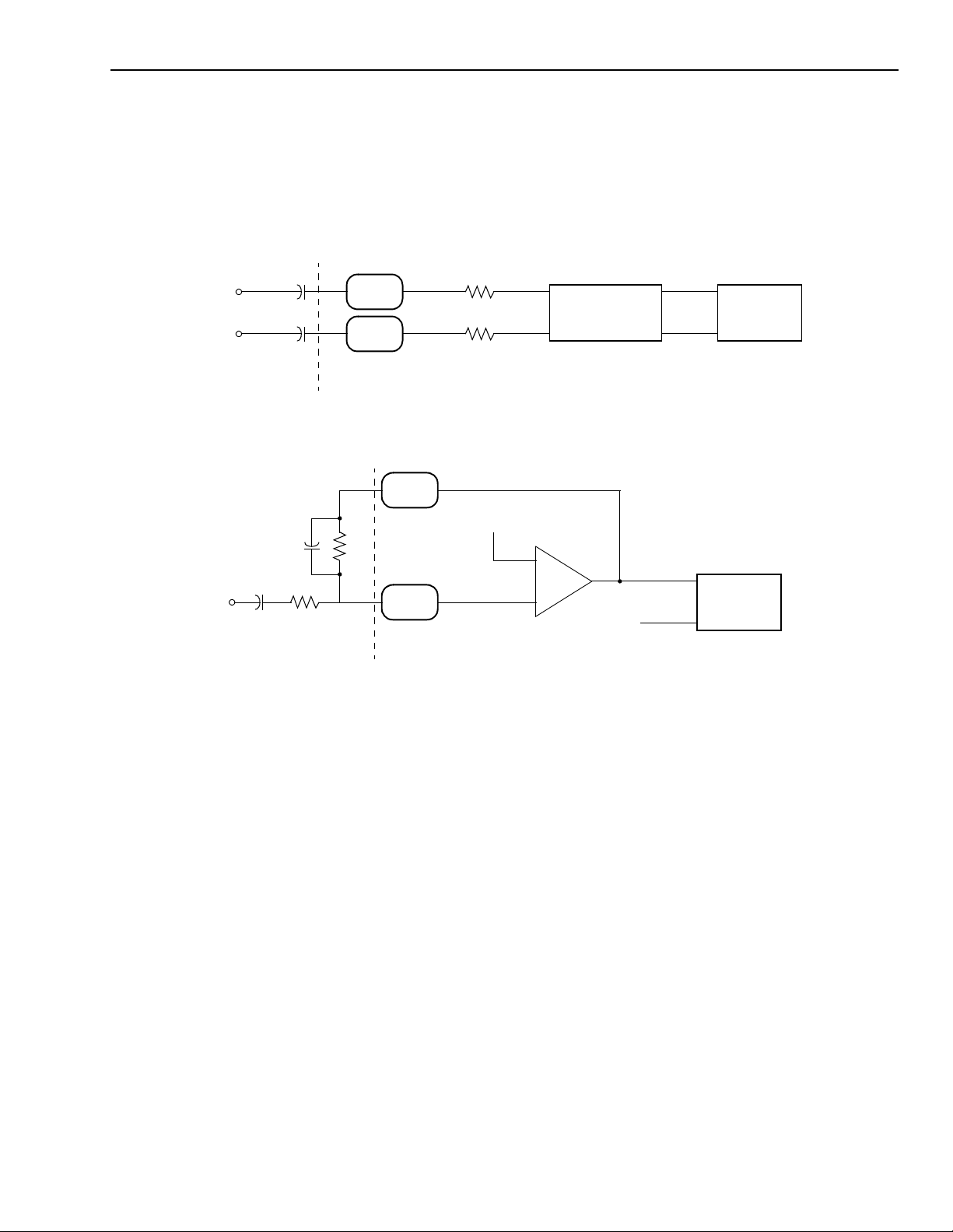
4.2.3 Analog Input Block
The A/D input block operates in two modes: when the
external input gain select (EIGS) pin is low or left
unconnected, the input goes through a preamplifier and
is band limited by a second-order 30 kHz low-pass antialiasing filter (see Figure 4 on page 7). When EIGS is
high, e xternal r esistor s, Rin and Rfb , are use d to set t he
gain of an inverting amplifier (see Figure 5 on page 7).
These resistors, in combination with Cin and Cfb, create a bandpass antialiasing filter. Note that EIGS is a
digital pin whose input levels are relative to digital
power and ground (V
and VSS).
DD
4.2.4 A/D Modulator and Digital Filters
A second-order ∆-Σ modulator quantizes the analog
signal to 1 bit (see Figure 3 on page 5). At the same
time, the resulting quantization noise is shaped such
that most of this noise lies outside of the baseband.
The modulator output is then digitally low-pass filtered
to remove the out-of-band quantization noise. After this
filtering, the output samples are decimated down to the
output sampling frequency. In the CSP1027, the filtering and decimation are completed in two stages. The
first-stage low-pass filter shapes the modulator output
according to the sinc-cubic transfer function:
4.2 Description of Signal Paths
4.2.1 Sampling Frequency
The oversampling ratio of the codec is 125:1; this is the
ratio of the frequency of the oversampling clock to the
frequency of the sampling clock. Most speech applications specify a sampling frequency of 8 kHz, yielding an
oversampling frequency of 8 kHz x 125 = 1.0 MHz. The
codec will operate at sampling frequencies up to
24 kHz, with the frequency response of the digital filters
being changed proportionally. For this architectural
description, the sampling frequency, f
be 8 kHz, with an oversampling frequency, f
1 MHz, unless otherwise stated.
6
, is assumed to
S
, of
OS
The output sampling frequency of the sinc-cubic filter is
reduced by a factor of 25 from 1 MHz to 40 kHz. The
sinc-cubic filter places nulls in the frequency response
at multiples of 40 kHz, and removes most of the quantization noise above 20 kHz so that very little energy is
aliased as a result of the decimation.
The sinc-cubic filter output is then processed by a
seventh-order IIR digital low-pass filter. This filter
removes the out-of-band quantization noise between
3.4 kHz and 20 kHz, compensates for the passband
droop caused by the sinc-cubic decimator, and decimates the sampling frequency by a factor of five from
40 kHz to 8 kHz.
Lucent Technologies Inc.
Data Sheet CSP1027 Voice Band Codec for
December 1999 Cellular Handset and Modem Applications
4 Architectural Information
(continued)
Following the low-pass filtering and decimation to 8 kHz, the 16-bit two's complement PCM can go directly to the
output register,
cdx(A/D)
, or go to a third-order IIR digital high-pass filter and then to the output register. The –3 dB
corner frequency of the high-pass filter is approximately 270 Hz. This filter exceeds the VSELP preprocessing
requirements of IS-54 for attenuation of 60 Hz and 120 Hz signals. The high-pass filter is selected by writing the
HPFE field in the
cioc3
register (see Table 10 on page 29). The default value upon reset is the high-pass filter
enabled (HPFE = 0).
Vin1
Vin2
EXTERNAL
COMPONENTS
Cin
MICIN
Cin
AUXIN
Rin
Rin
PREAMPLIFIER
AND AA-FILTER
+
AND
FILTERS
–
A/D
5-7592 (F)
Figure 4. CSP1027 A/D Path When in the Preamplifier Mode (EIGS = 0)
AUXIN
INTERNAL
SIGNAL GND
RfbCfb
RinCin
MICIN
EXTERNAL
COMPONENTS
–
+
INTERNAL
SIGNAL GND
+
FILTERS
–
A/D
AND
5-7593 (F)
Figure 5. CSP1027 A/D Path in the External Gain Select Mode (EIGS = 1)
4.2.5 A/D Path Frequency Response
The composite digital filters (decimator, LPF, and HPF)
meet the ITU-T G.712 voice band frequency response
specifications and are suitable for IS-54, JDC, and
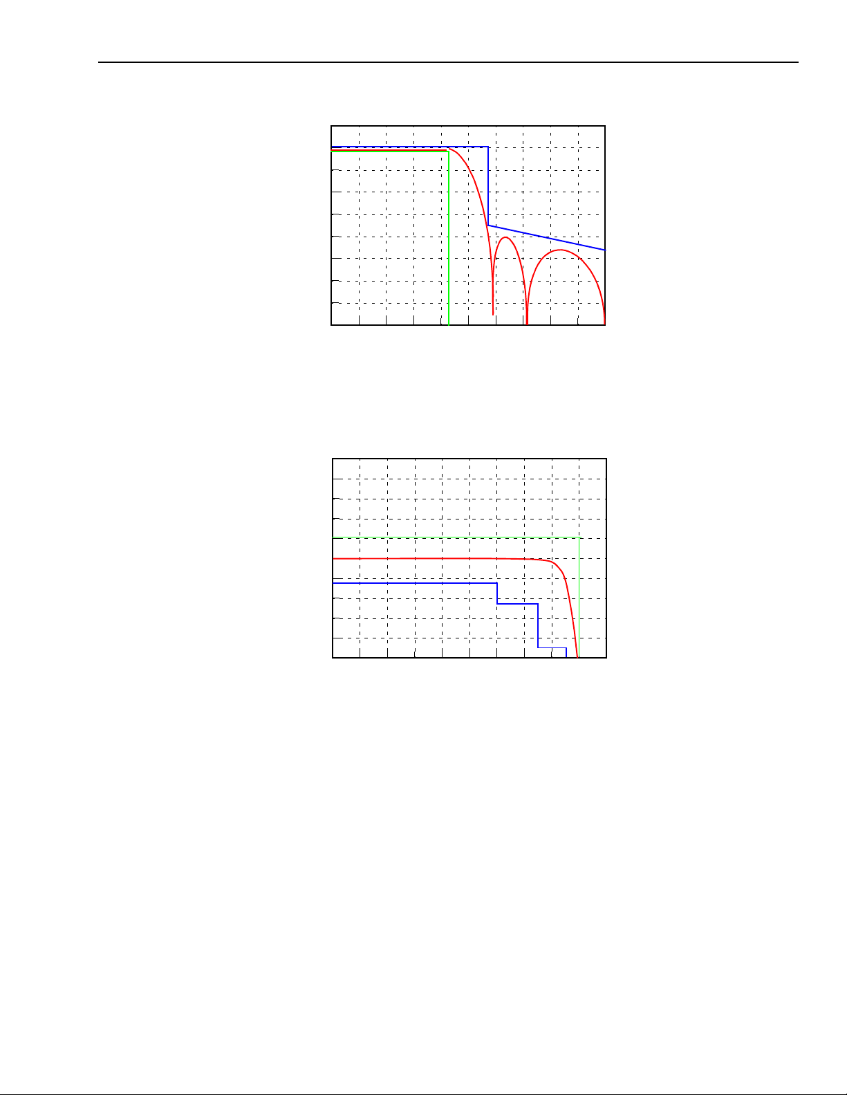
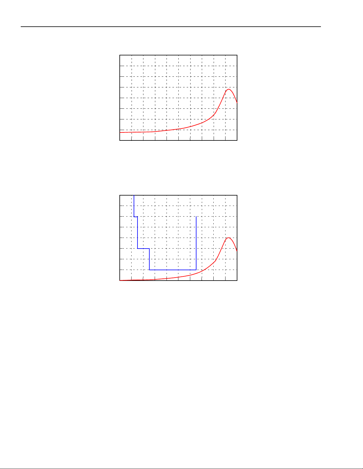
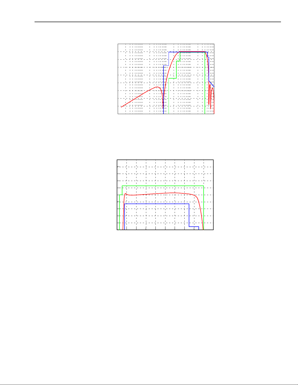
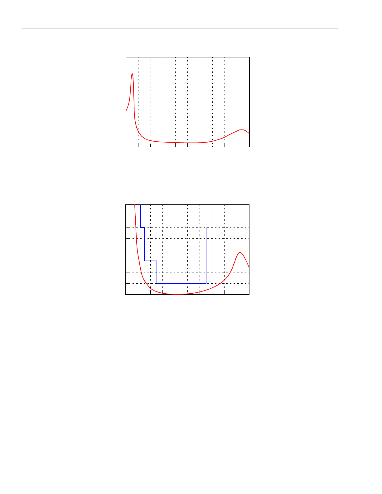
GSM digital cellular applications. Figures 6 through 9
show the A/D and D/A frequency response without the
optional high-pass filter (HPF). Figures 10 and 11 show
the group delay characteristics of the A/D and D/A without the high-pass filter. Figures 12 and 13 show the frequency response of the high-pass filter. Figures 14 and
15 show the group delay characteristics of the highpass filter. In all figures, the frequency is normalized to
the sampling frequency f
(i.e., frequency/fS). T o get the
S
actual frequency, multiply the normalized frequency by
f
. The absolute delay and delay distortion have been
S
normalized to the sampling period 1/f
(i.e., delay x fS).
S
Lucent T echnologies Inc.
To obtain the actual delay, divide the normalized delay
by f
. The templates shown in Figures 7 through 9,
S
11 through 13, and 15 correspond to the limits in the
ITU-T G.712 specification where f
= 8.0 kHz.
S
4.2.6 PCM Saturation Versus Analog Input Levels
16-bit two's complement saturation is employed to prevent wraparound during input overload conditions. The
saturation is hard-limiting:
0x7fff = maximum positive level
0x8000 = minimum negative level
The analog levels that correspond to the saturation lev-
els for the three input modes are outlined in T ab le 14 on
page 51.
7

CSP1027 Voice Band Codec for Data Sheet
Cellular Handset and Modem Applications December 1999
4 Architectural Information
–20
–40
–60
–80
LOG MAGNITUDE (dB)
–100
–120
Figure 6. A/D or D/A Path Frequency Response Over 5.0 f
10
–10
–20
–30
–40
–50
LOG MAGNITUDE (dB)
–60
–70
–80
(continued)
20
0
0.0 0.5 1.0 1.5 2.0 2.5 3.0 3.5 4.0 4.5 5.0
FREQUENCY (fs = 1)
Bandwidth (HPF Disabled)
S
0
0.0 0.5 1.0 1.5 2.0 2.5
5-7594 (F)
FREQUENCY (fs = 1)
5-7595 (F)
Figure 7. A/D or D/A Path Frequency Response Over 2.5 f
8
Bandwidth (HPF Disabled)
S
Lucent Technologies Inc.
Data Sheet CSP1027 Voice Band Codec for
)
December 1999 Cellular Handset and Modem Applications
4 Architectural Information
10
–10
–20
–30
–40
–50
LOG MAGNITUDE (dB)
–60
–70
–80
Figure 8. A/D or D/A Path Frequency Response Over f
1.0
0.8
0.6
0.4
0.2
0.0
–0.2
–0.4
LOG MAGNITUDE (dB)
–0.6
–0.8
–1.0
(continued)
0
0.0 0.1 0.2 0.3 0.4 0.5 0.6 0.7 0.8 0.9 1.0
FREQUENCY (fs = 1)
Bandwidth (HPF Disabled)
S
0.00 0.05 0.10 0.15 0.20 0.25 0.30 0.35 0.40 0.45 0.50
5-7596 (F
Figure 9. A/D or D/A Path Frequency Response Over 0.5 f
Lucent T echnologies Inc.
FREQUENCY (fs = 1)
Bandwidth (HPF Disabled)
S
5-7597 (F)
9
CSP1027 Voice Band Codec for Data Sheet
Cellular Handset and Modem Applications December 1999
4 Architectural Information
ABSOLUTE DELAY (# OF SAMPLES)
Figure 10. A/D or D/A Path Absolute Group Delay (HPF Disabled)
(continued)
8
7
6
5
4
3
2
1
0
0.0 0.05 0.10 0.15 0.20 0.25 0.30 0.35 0.40 0.45 0.50
FREQUENCY (fs = 1)
8
7
5-7598 (F)
6
5
4
3
2
1
DELAY DISTORTION (# OF SAMPLES)
0
0.0 0.05 0.10 0.15 0.20 0.25 0.30 0.35 0.40 0.45 0.50
FREQUENCY (fs = 1)
Figure 11. A/D or D/A Path Group Delay Distortion (HPF Disabled)
5-7599 (F)
10
Lucent Technologies Inc.
Data Sheet CSP1027 Voice Band Codec for
December 1999 Cellular Handset and Modem Applications
4 Architectural Information
–10
–20
–30
–40
–50
LOG MAGNITUDE (dB)
–60
–70
–80
Figure 12. A/D or D/A Path Frequency Response Over f
1.0
0.8
0.6
0.4
0.2
0.0
–0.2
–0.4
LOG MAGNITUDE (dB)
–0.6
–0.8
–1.0
(continued)
10
0
–4
10
0.00 0.05 0.10 0.15 0.20 0.25 0.30 0.35 0.40 0.45 0.50
–3
10
FREQUENCY (fs = 1)
10
–2
–1
10
Bandwidth (HPF Enabled)
S
10
0
5-7600 (F)
Figure 13. A/D or D/A Path Frequency Response Over 0.5 f
Lucent T echnologies Inc.
FREQUENCY (fs = 1)
Bandwidth (HPF Enabled)
S
5-7601 (F)
11
CSP1027 Voice Band Codec for Data Sheet
Cellular Handset and Modem Applications December 1999
4 Architectural Information
25
20
15
10
ABSOLUTE DELAY (# OF SAMPLES)
Figure 14. A/D or D/A Path Absolute Group Delay (HPF Enabled)
(continued)
5
0
0.00 0.05 0.10 0.15 0.20 0.25 0.30 0.35 0.40 0.45 0.50
FREQUENCY (fs = 1)
5-7602 (F)
8
7
6
5
4
3
2
1
DELAY DISTORTION (# OF SAMPLES)
0
0.00.050.100.150.200.250.300.350.400.450.50
FREQUENCY (fs = 1)
Figure 15. A/D or D/A Path Group Delay Distortion (HPF Enabled)
5-7603 (F)
12
Lucent Technologies Inc.

Data Sheet CSP1027 Voice Band Codec for
December 1999 Cellular Handset and Modem Applications
4 Architectural Information
(continued)
4.2.7 Digital-to-Analog Path
Starting at the bottom right of Figure 3 on page 5, the
∆-Σ D/A conversion process begins with a 16-bit two's
complement PCM signal read from the DI serial input.
The PCM is interpolated up to 1 MHz in two stages and
low-pass filtered at each stage to attenuate 8 kHz
images.
The PCM input is latched into the
cdx(D/A)
register at
a nominal word rate of 8 kHz. The signal is then optionally high-pass filtered. This filter has the same transfer
function as the A/D high-pass filter.
A digital sample-and-hold increases the word rate by a
factor of 5 from 8 kHz to 40 kHz. The seventh-order IIR
digital low-pass filter then removes the spectral images
between 4 kHz and 20 kHz and predistorts the passband to compensate for the filtering done during the
interpolation up to the 1 MHz word rate. The transfer
function of this low-pass filter is the same as the one
employed in the A/D converter.
The output of the low-pass filter feeds a programmable
gain adjustment block that serves as a volume control.
The gain can be changed in 3 dB increments from
0 dB to –45 dB. The attenuation level is set by writing
the OGSEL field in the
cioc0
register (see Table 7 on
page 26).
The digital modulator block further increases the word
rate by a factor of 25 from 40 kHz to 1 MHz. Through
quantization and noise shaping, the digital ∆-Σ modulator creates 1-bit output words at 1 MHz.
The modulator 1-bit output drives a structure combining
a 1-bit D/A converter and a second-order switchedcapacitor filter having a cutoff frequency of 8 kHz
(based on a 1 MHz clock). This is all shown as the D/A
block in Figure 3 on page 5.
4.3 Programmable Features
4.3.1 Active/Inactive Modes
The CSP1027 has active and inactive modes of operation which are selected by the ACTIVE field in the
cioc0
register (see Table 7 on page 26). The default
value upon reset and powerup is ACTIVE = 0 (i.e.,
inactive). In the inactive mode, the codec clocks are
disabled, data transfers by the codec are disabled, and
analog bias currents are shut off. This state is useful in
battery-powered applications when prolonged periods
of inactivity are expected. It takes approximately
600 ms for the codec to reach full steady-state performance in going from inactive to active. This is primarily
due to the charging of the large external capacitors,
C
and C
REF
useful after 100 ms.
4.3.2 Input Select
When the A/D preamplifier is selected (EIGS = 0), the
INSEL field of
the preamp input between the MICIN and AUXIN
inputs. When external gain select is used (EIGS = 1),
the INSEL field has no effect.
4.3.3 A/D Input Ranges
When the preamplifier is used (EIGS = 0), the IRSEL
field of the
selects the 500 mVp range when IRSEL = 0 and the
160 mVp range when IRSEL = 1. IRSEL has no effect
when the external gain select mode is used (EIGS = 1).
When EIGS = 1, the inverting amplifier of Figure 5 on
page 7 replaces the preamplifier. The input range in
this mode is the following:
. However, the codec is functionally
REG
cioc0
(see Table 7 on page 26) switches
cioc0
register (see T able 7 on page 26)
Rin
--------- -
FULL-SCALE
V
=
Rfb
1.578 V p
×
This is followed by a second-order active Chebychev filter having a cutoff frequency of 35 kHz.
The passband ripple of the analog filters is small
enough such that they have virtually no effect on the
passband response.
The output amplifier buffers the analog filter output.
The frequency responses of the A/D and D/A paths are
essentially the same. See Figures 6 through 15 for the
magnitude and delay responses versus frequency.
Lucent T echnologies Inc.
4.3.4 Output Mute Function
The D/A converter output can be selectively muted with
the MUTE field in the
cioc0
register (see Table 7 on
page 26). The default value upon reset is muted
(MUTE = 0). The mute function is implemented (Figure
3 on page 5) internally by a MUX following the D/A
input. Placing the mute function here causes the signal
at the analog output to gradually decay/rise over
approximately 1 ms upon muting/unmuting. This effect
is due to the impulse response and group delay of the
digital filters. This implementation will reduce any
potentially undesirable transient effects such as pops,
when the D/A is muted.
13

CSP1027 Voice Band Codec for Data Sheet
Cellular Handset and Modem Applications December 1999
4 Architectural Information
(continued)
4.3.5 Output Gains
The D/A converter output can be programmed in 3 dB
increments with the OGSEL field in the
cioc0
register
(see Table 7 on page 26) to serve as a volume control.
4.3.6 Loopback Mode
The codec has a programmable loopback mode, represented by the TEST field in the
cioc0
register, (see
Table 7 on page 26). As shown in Figure 3 on page 5,
when TEST = 0, the codec is in its normal mode of
operation. When TEST = 1, the loopback mode is activated. In loopback mode, the 1-bit PDM output signal
from the analog modulator is received by the analog
demodulator. At the same time, the 1-bit signal output
from the digital modulator is received by the sinc-cubic
filter in the A/D. This results in the analog input being
looped back to the analog output through the A/D and
D/A, and the digital input being looped back to the digital output through the digital filters. The loopback mode
can be useful for evaluating analog performance of the
codec in the target system without going through the
digital filters. This mode is also useful for evaluating the
response of the digital filters or in evaluating the read/
write functions of the
codec
and
cdx
registers without
having to provide an analog input to the A/D.
4.3.7 High-Pass Filter Select
The high-pass filter in the A/D and D/A can be enabled
or disabled with the HPFE field in the
cioc3
register
(see Table 10 on page 29).
4.3.8 Dither
A dithering scheme is employed in the CSP1027 which
decorrelates the periodic quantization noise of the D/A
modulator to make it white noise.
The DITHER field in the
cioc3
register (see Table 10
on page 29) disables this feature. The default value
upon reset is DITHER = 0 (i.e., enabled). When the
DITHER is disabled, the signal-to-noise ratio will generally be about 2 dB higher. The DITHER should be
enabled if the CSP1027 is used in an audio application,
i.e., where this device interfaces to an audio transducer. If the CSP1027 is used in an application other
than audio, such as data communications, the DITHER
can be disabled if so desired.
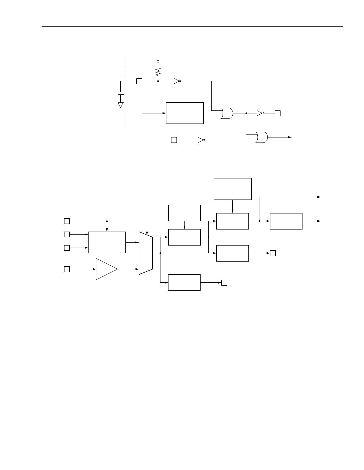
4.4 Power-On Reset
4.4.1 Internal
The CSP1027 has a power-on reset circuit that is
ORed internally with the inversion of the reset pin,
RSTB, to form the internal reset (see Figure 16 on
page 15). The power-on reset circuit’s inverted output
is also an output pin, PORB. The PORB can be used to
provide power-on reset to the system.
The power-on reset circuit is composed of two pulsegenerating elements, its output being the OR of the
two. One element is entirely internal and generates a
power-on pulse of 1.5 ms to 7.0 ms. The second element is composed of an input pin, PORCAP, a resistor
connected between PORCAP and V
ing input buffer. The user selects the capacitor value to
connect between PORCAP and ground that will generate a power-on pulse of desired width. The pin
PORCAP allows the user to lengthen the power-on
reset pulse to a width greater than the internal poweron element provides. The nominal value of the resistor
is 155 kΩ, and the threshold of the inverting input buffer
is 0.6 x V
. The formula that relates the power-on
DD
reset pulse delay to the PORCAP capacitor is as follows:
D
T
= –R x C x loge (1 – 0.6)
D
T
= 0.9163 x R x C
, and an invert-
DD
∆-Σ converters are popular due to their high tolerance
to component mismatch present in integrated circuit
fabrication processes. However, ∆-Σ converters may
suffer from periodic noise and spurious tone generation
(in-band and out-of-band) due to the coarse quantization and feedback of the ∆-Σ modulator. Although this
periodic noise may exist at very low levels (f or example,
at about –90 dBm), it may be very objectionable to the
listener while having virtually no impact on the resolution of the converter. The CSP1027 D/A uses a robust
dithering scheme which eliminates any potential problems due to this phenomenon.
14
Hence, to generate a 14.2 ms power-on reset pulse,
one would use a 0.1 µF capacitor connected between
PORCAP and V
SS
.
An internal power-on pulse can be initiated after poweron by writing a one to the TSTPOR field in the
cioc3
register (see T able 10 on page 29). This causes the
internal power-on pulse of 1.5 ms to 7.0 ms to be generated. The pulse resets the device and appears on the
PORB output pin.
Lucent Technologies Inc.
Data Sheet CSP1027 Voice Band Codec for
December 1999 Cellular Handset and Modem Applications
4 Architectural Information
PORCAP
C
EXTERNAL
COMPONENT
XOSCEN
XLO
XHI
CLK
ENABLE
OSCILLATOR
(continued)
DD
V
R
TSTPOR
POWER-ON
PULSE
GENERATOR
RSTB
Figure 16. Power-On Reset Diagram
CDIFS, CDIF0,
CDIF1, CDIF2,
CDIV3
ADJMOD,
ADJ
÷
F1
÷
ICLK
CDIV0
÷
CDIV2
1
M
U
X
0
ICLK0
CKO2
÷
CDIV1
CKO1
PORB
INTERNAL
RESET
CK
÷
125
OS
CK
5-7604 (F)
S
Lucent T echnologies Inc.
5-7560 (F)
Figure 17. Clock Generation
15
CSP1027 Voice Band Codec for Data Sheet
Cellular Handset and Modem Applications December 1999
4 Architectural Information
(continued)
4.5 Clock Generation
Figure 17 on page 15 shows the clock generation and
distribution for the CSP1027. The programmable dividers can customize the codec sample and master clock
rates for a variety of applications in addition to standard
8 kHz sampling, while allowing a range of values for
the crystal-controlled input clock. In Figure 17 on page
15, XOSCEN is a chip input to enable the crystal oscillator circuit. XLO and XHI are the two leads for the
crystal. CLK is the chip clock input if the crystal is not
used. CK
8 kHz. CK
typically 1 MHz. CKO1 and CKO2 are general-purpose
clocks brought out to chip pins. CDIV1 and CDIV2 are
programmable dividers with a range fr om 1 to 31.
CDIV0 is programmed to be 1 or 2, but extra clock
pulses can be added or subtracted at the output for one
period of time following a write to the control register
cioc1
ber of clocks is programmed by ADJMOD and ADJ and
causes a phase shift in the CKO1 and CK
is an integral or a fractional divider controlled by the
five programmable coefficients shown connected to it.
With the fractional divide, the period of CK
but the period of CK
The following discussion begins with the crystal oscillator and is followed by a detailed description of each
divisor block. Section 7.5 on page 45 provides some
examples of how to program the clocks.
4.5.1 Crystal Oscillator
The CSP1027 has a selectable on-chip clock oscillator.
A logic 1 on the XOSCEN pin enables the crystal oscillator. A logic 0 disables the oscillator, powers it down,
and selects the input buffer connected to the CLK pin.
To use the oscillator, select a 20 MHz to 30 MHz fundamental-mode crystal with a series resistance less than
60 Ω and a mutual capacitance less than 7.0 pF. Connect the crystal between the XLO and XHI pins, and
add 10 pF capacitors between XLO and ground, and
XHI and ground. The XOSCEN pin enables and disables the crystal oscillator. See the application information on optimizing the oscillator performance.
is the internal codec sample clock, typically
S
is the internal codec oversampled clock,
OS
. This one-time increase or decrease in the num-
output. F1
S
will vary,
OS
will be constant.
S
4.5.2 Clock Divider 2
ICLK CKO2
÷
CDIV2
5-7589 (F)
Figure 18. Clock Divider 2
The CDIV2 field in
cioc0
(see Table 7 on page 26) sets
the clock divider that generates the output clock,
CKO2. The clock output is a general-purpose clock that
can be used to clock external logic or processors.
CDIV2 ranges from 1 to 31, with 0 holding the output
low. RSTB going low sets CDIV2 to ÷16. CKO2 is
active while RSTB is low and synchronized by RSTB
going high.
4.5.3 Clock Divider 0
ADJMOD,
ADJ
ICLK ICLK0
÷
CDIV0
5-7588 (F)
Figure 19. Clock Divider 0
The CDIV0 field in
cioc1
(see Table 8 on page 27) sets
the clock divider that generates the internal clock 0
(ICLK0) to either divide by one or divide by two. The
ADJMOD and ADJ fields in
cioc1
are used to adjust
the phase of ICLK0 by increasing or decreasing the
rate of ICLK0 for a burst of pulses, one time only. This
event occurs each time control register
cioc1
is written
with nonzero values of ADJ. For example, let CDIV0 be
set to ÷2, ADJ to seven, and ADJMOD to one
(advance). After this word is written to the
cioc1
register, seven ICLK0 pulses will occur at the same rate as
ICLK, not divided by two. These seven clock pulses
shift the phase of CK
, CKS, and CKO1 earlier, thus
OS
advancing these clocks. If ADJMOD is set to zero
(retard), the ÷2 becomes a ÷3 for seven pulses of
ICLK0. The CDIV0 clock divider is temporarily changed
internally so that it divides by one greater, to retard the
clocks, or one less, to advance the clocks, for the specified number of ICLK0 cycles. Note that the CDIV0
clock divider must be set to divide by two in order to
advance and retard the clocks. If CDIV0 clock divider is
set to divide by 1, one can only retard the clocks.
16
Lucent Technologies Inc.
Data Sheet CSP1027 Voice Band Codec for
F1 M S
N
125
--------- -
×
+=
fSf
OS
125÷f
ICLK
0
MS
N
125
--------- -
×+
÷
125
÷==
f
ICLK
0
f
S
----------------
125 M
×()
SN
×()+=
1
f
S
---- -
125 N
–()
M
f
ICLK
0
----------------
×
N
MS
+()
f
ICLK
0
--------------------
×+=
December 1999 Cellular Handset and Modem Applications
4 Architectural Information
(continued)
CDIV0 has values of 1 or 2, ADJMOD is 0 or 1, and
ADJMOD ranges from 1 to 127, with 0 selecting no
clock adjust. RSTB going low sets CDIV0 to ÷2. ICLK0
is active while RSTB is low and synchronized by RSTB
going high.
4.5.4 Clock Divider 1
ICLK0 CKO1
÷
CDIV1
5-7587 (F)
Figure 20. Clock Divider 1
The CDIV1 field in
cioc1
(see Table 8 on page 27) sets
a clock divider that generates the CKO1 output clock.
This general-purpose clock output can be used for
clocking another codec in the system, such as the
CSP1084. The ability to phase adjust the output clock
and the codec sampling clock simultaneously is an
important feature. CDIV1 ranges from 1 to 31, with 0
disabling the output. RSTB going low sets CDIV1
to ÷16. CKO1 is active while RSTB is low and synchronized by RSTB going high.
4.5.5 Sampling Clocks Generation
CDIFS, CDIF0, DSIF1,
CDIF2, CDIV3
OS
CK
The CSP1027 solves this problem in a unique way, by
providing a programmable, fractional divider, F1.
F1 is the programmable ratio between ICLK0 and
CK
. The equation for F1 is:
OS
where 3 ≤ M ≤ 64, 0 ≤ N ≤ 62, and S = {1, –1};
or M = 2, 0 ≤ N ≤ 62, and S = 1;
or M = 1, N = 0, and S = 1.
M is encoded by CDIV3 (see Table 3 on page 18), N is
encoded by CDIF0, CDIF1, and CDIF2 (see Table 5 on
page 19), and S is encoded by CDIFS (see Table 4 on
page 18).
CK
is generated by dividing CKOS by 125. The fre-
S
quency of CK
can be described by:
S
Note that when N = 0, ICLK0 is simply divided by the
integer M to create the oversampling clock, CK
OS
. This
is the preferred method for generating the sampling
clock. If N ≠ 0, the fractional division results in an oversampling clock, CK
, whose period varies with time
OS
such that the average period is the desired fraction.
This vari ation in the oversampling clock period is minimized by the clock generator but can cause distortion
in the codec. Because the denominator of the fraction
is fixed at 125, the period of the sampling clock, CK
S,
will be an integer multiple of the period of the internal
clock, ICLK0, and will not vary. This is more clearly
shown by the following equation:
ICLK0
÷
F1
÷
125
CK
S
The expanded equation below explains what is happening in the time domain:
5-7586 (F)
Figure 21. Sampling Clocks Generation
1
During each sampling period, , there are (125 – N)
The oversampling codec clock CK
is used in the front sections of the A/D and the back
, typically 1 MHz,
OS
oversampling clock cycles of period and N
sections of the D/A. The lower-frequency codec clock,
CK
, typically 8 kHz, is the sample clock at th e output
S
oversampling clock cycles of period . The N
of the A/D and the input to the D/A. The sampling clock
frequency, f
, is the oversampling clock frequency, fOS,
S
divided by 125 (the fixed oversampling ratio). The
divide by 125 must remain fixed, since it is constrained
by the architecture of the codec digital filters. Many systems, however, have fixed high-frequency clocks and
fixed sampling clocks, so it is necessary to have a great
deal of flexibility in the creation of the codec clock CK
oversampling clock cycles are evenly distributed
among the (125 – N) oversampling clock cycles to minimize the distortion due to oversampling clock cycles of
differing period. The values for CDIF[0—2] in Table 5
on page 19 have been selected to achieve the even
distribution.
.
S
Lucent T echnologies Inc.
---- -
f
S
M
----------------
f
ICLK
0
MS
()
+
------------------- -
f
ICLK
0
17
CSP1027 Voice Band Codec for Data Sheet
Cellular Handset and Modem Applications December 1999
4 Architectural Information
The procedure for selecting M, S, and N is illustrated in Section 7.5 on page 45. The ranges for the programmable
dividers are summarized in Table 2.
Table 2. Programmable Divider Summary
Clock Ratio ICLK/ICLK0 ICLK0/CK
Variable Name CDIV0
Range of Values 1, 2 1, 2 to 64.496 125, 250 to 8062 Off, 1 to 31 Off, 1 to 31
Encoding 0, 1 See Tables 3
Table 3. CDIV3 Value for Each M
M CDIV3
1 00 0001
2 00 0010
.
.
62 11 1110
63 11 1111
64 00 0000
.
.
(continued)
N
--------- -
M
±
125
through 5.
OS
ICLK0/CKS ICLK/CKO2 ICLK0/CKO1
125M ± N
See Tables 3
through 5.
CDIV2 CDIV1
0 to 31 0 to 31
Table 4. CDIFS Value for Each S
S CDIFS
+1 0
–1 1
18
Lucent Technologies Inc.

Data Sheet CSP1027 Voice Band Codec for
December 1999 Cellular Handset and Modem Applications
4 Architectural Information
Table 5. CDIF0, CDIF1, CDIF2 Values for Each N
N CDIF0 CDIF1 CDIF2 N CDIF0 CDIF1 CDIF2
0 00 0000 00 0000 0 0000 32 00 0100 10 1000 0 0010
1 11 1111 00 0000 0 0000 33 00 0100 10 0100 0 0010
2 11 1101 00 0010 0 0000 34 00 0011 00 0010 1 0010
3 10 1001 00 0010 0 0000 35 00 0011 00 0010 1 0100
4 01 1111 00 0000 0 0000 36 00 0011 00 0010 0 0100
5 01 1001 00 0000 0 0000 37 00 0011 00 0011 1 0010
6 01 0101 10 0110 0 0000 38 00 0011 00 0011 0 0010
7 01 0010 10 0100 0 0000 39 00 0011 00 0100 0 0010
8 00 1111 00 0010 0 0000 40 00 0011 00 0111 0 0000
9 00 1110 10 0101 0 0000 41 00 0011 00 1110 0 0000
10 00 1100 00 0010 0 0000 42 00 0011 11 0110 0 0000
11 00 1011 00 0010 0 0010 43 00 0011 10 1001 0 0000
12 00 1010 00 0010 0 0010 44 00 0011 10 0110 0 0000
13 00 1001 00 0010 1 0010 45 00 0011 10 0100 0 0010
14 00 1001 10 0111 0 0010 46 00 0011 10 0011 0 0010
15 00 1000 00 0011 0 0000 47 00 0010 00 0010 1 0010
16 00 1000 10 0100 0 0010 48 00 0010 00 0010 1 0011
17 00 0111 00 0011 0 0000 49 00 0010 00 0010 1 0101
18 00 0111 10 1001 0 0010 50 00 0010 00 0010 0 0000
19 00 0110 00 0010 1 0011 51 00 0010 00 0010 0 0011
20 00 0110 00 0011 0 0010 52 00 0010 00 0010 0 0010
21 00 0110 10 1011 0 0000 53 00 0010 00 0011 1 0011
22 00 0101 00 0010 1 0010 54 00 0010 00 0011 0 0011
23 00 0101 00 0010 0 0010 55 00 0010 00 0011 0 0010
24 00 0101 00 0100 0 0010 56 00 0010 00 0100 0 0010
25 00 0101 00 0000 0 0000 57 00 0010 00 0101 0 0000
26 00 0101 10 0100 0 0010 58 00 0010 00 0110 0 0000
27 00 0100 00 0010 1 0011 59 00 0010 00 0111 0 0010
28 00 0100 00 0010 0 0011 60 00 0010 00 1010 0 0010
29 00 0100 00 0011 0 0000 61 00 0010 00 1111 0 0010
30 00 0100 00 0101 0 0010 62 00 0010 00 0000 0 0000
31 00 0100 00 0000 0 0000
(continued)
Lucent T echnologies Inc.
19

CSP1027 Voice Band Codec for Data Sheet
Cellular Handset and Modem Applications December 1999
4 Architectural Information
(continued)
4.6 Serial I/O Configurations
4.6.1 Codec Data Transfer
When the codec is active, ACTIVE = 1 (see Table 7 on
page 26), it loads data into the
data from the
cdx(D/A)
register (see Figure 3 on page
5) at the sampling frequency, f
on a 1 MHz oversampling frequency). The codec data
transfers occur independent of the serial input/output
data transfers described below. The data is double
buffered, allowing the codec to transfer data to or from
cdx
the
the shift registers (
while the serial I/O is shifting data into or out of
isr
and
to inactive, ACTIVE = 0, there are no codec data transfers to the
cdx(A/D)
or from the
The internal STATUS flag is set high when
loaded and
cdx(A/D)
cdx(D/A)
is emptied. Loading data from the
into the output shift register (
data from the input shift register (
due to a serial I/O transaction, clears the internal STATUS flag. The internal STATUS flag can be observed
on the data output (DO) pin in the passive mode and
causes data transfers in the active and multiprocessor
modes.
4.6.2 Codec Control Writes
The four control registers are written through the serial
port. The serial address (SADD) selects between control and data transfers. Bits 15 and 14 of the control
word being transferred select which control register,
cioc0, cioc1, cioc2
Bit[15:14] = 00,
cioc1
cioc3
, or
: Bit[15:14] = 01, etc.).
4.6.3 Serial I/O Port Overview
The CSP1027 serial I/O unit is an asynchronous, fullduplex, double-buffered channel operating at up to
20 Mbits/s that easily interfaces with other Lucent fixedpoint DSPs (i.e., DSP16A and DSP1610/1616/1617/
1618) in a single or multiple DSP environment. Commercially available codecs and time-division multiplexed (TDM) channels can be interfaced to the
CSP1027 device with little, if any, external logic.
cdx(A/D)
(which is 8 kHz based
S
osr
). When the codec is set
cdx(D/A)
and empties
.
cdx(A/D)
osr
) or loading
isr
) into the
, is written (i.e.,
cdx(D/A)
cioc0
is
:
The serial interface is a subset of the standard Lucent
DSP serial I/O and is comprised of eight pins:
■ A single passive serial input/output clock (IOCK).
■ A combined input load, output load, and synchroni-
zation (SYNC).
■ Serial data input (DI).
■ Serial data output (DO).
■ Serial address (SADD).
■ Three serial mode select pins (SMODE[2:0]).
The CSP1027's serial I/O is different from the standard
Lucent serial I/O in a number of ways:
■ The SMODE[1:0] pins configure the serial I/O port
into one of four possible ways: a passive SIO configuration, an active SIO configuration, and two multiprocessor SIO configurati ons.
■ A fixed most significant bit (MSB) first data format.
■ A fixed 16-bit data mode.
■ The serial address (SADD) is an input during the
passive and active SIO configurations to select
between data and control SIO transfers. It is
intended to be connected to the DSP’s SADD pin,
which is an output during passive and active SIO.
Note that the DSP's SADD output is inverted and is
composed of two 8-bit fields that are shifted out least
significant bit (LSB) first.
■ The multiprocessor mode time slots and serial
addresses are restricted to two sets, one of which is
selected based on the state of SMODE0.
■ The SMODE2 pin should always be tied low for the
serial I/O port to operate as described.
■ The frequency of the serial I/O interface clock input
IOCK (F
the internal oversampling clock (F
IOCK
) must be greater than the frequency of
IOCK
).
20
Lucent Technologies Inc.

Data Sheet CSP1027 Voice Band Codec for
December 1999 Cellular Handset and Modem Applications
4 Architectural Information
SMODE0
SMODE1
SMODE2
DO
DI
(continued)
IOCK
SADD
SYNC
D/A DATA
A/D DATA
CLOCK
CONTROL/DATA ADDRESS
INPUT/OUTPUT LOAD
Figure 22. Passive Communication and Connections
4.6.4 Passive I/O Configuration (SMODE[1:0] = 00)
The passive SIO configuration allows the user maximum flexibility in interfacing the CSP1027 to a variety
of system hardware configurations. It requires that the
user supply a serial input/output clock (IOCK) and perform data transfers at the sampling rate, f
. Serial data
S
transfers can be made to occur at the sampling rate by
applying a clock that is synchronous with the codec
clock, ICLK, to the SYNC pin or by polling the codec
STATUS flag, which indicates that the
ter is full and the
cdx(D/A)
register is empty. The STA-
cdx(A/D)
regis-
TUS flag appears on DO when the SADD pin selects a
control word.
Passive SIO is selected by setting both SMODE1 and
SMODE0 low. The input/output clock (IOCK) is an input
and the common input/output load, SYNC, (equivalent
to a DSP16A's ILD and OLD tied together) is also an
input. Serial data input (DI) is an input and serial data
output, DO, is an output. The serial address (SADD) is
an input, which determines if the transfer is to the control registers,
cioc
[0:3], or the data register,
cdx(D/A)
.
A high-to-low transition of SYNC pin signal, latched by
the next rising edge of IOCK, initiates the start of an
input and output transaction. If the CSP1027's output
DSPCSP1027
DO
cdx(A/D)
buffer,
shift register (
ICK
DI
, is full, it will be loaded into the output
osr
) and shifted out on the DO pin. The
OCK
SADD
ILD
OLD
5-7590 (F)
CSP1027 shifts in the data from the DI pin into its input
shift register (
isr
). A serial transmit address on the
SADD line is received simultaneously with data on the
DI line. If SADD is high for the first 15 bits, corresponding to a zero serial transmit address, this causes the
to be latched into
cdx(D/A)
after 16 bits have been
isr
shifted in. If SADD is low for any of the first 15 bits, corresponding to a nonzero transmit address, this causes
isr
the
to be latched into
cioc
[0:3] and also changes
the output data stream on DO to display the internal
codec STATUS flag. If SADD is low for any clock cycle,
while not involved in a serial transaction, the codec
STATUS flag is displayed on the DO pin until the next
data transfer.
An example of the passive SIO configuration is shown
in Figure 22. The DSP supplies both the serial clock
(IOCK) and the sampling synchronization signal to
SYNC, or polls the internal codec STATUS flag to
determine when a data transmission is needed. This
configuration allows the user maximum flexibility in
interfacing the CSP1027 to a variety of other system
hardware configurations.
Lucent T echnologies Inc.
21

CSP1027 Voice Band Codec for Data Sheet
Cellular Handset and Modem Applications December 1999
4 Architectural Information
DD
V
SMODE0
SMODE1
SMODE2
DO
DI
(continued)
IOCK
SADD
SYNC
D/A DATA
A/D DATA
CLOCK
CONTROL/DATA ADDRESS
INPUT/OUTPUT LOAD
Figure 23. Active Communication and Connections
4.6.5 Active I/O Configuration (SMODE[1:0] = 01)
The active SIO configuration causes the CSP1027 to
generate an active input/output load (SYNC) to perform
input/output transmissions when needed. The user
supplies only a serial input/output clock (IOCK).
The active SIO is selected by setting SMODE1 low and
SMODE0 high. The input/output clock (IOCK) is an
input and the input/output load (SYNC) is an output.
While the codec is inactive, ACTIVE = 0 (see Table 7
on page 26), SYNC generates serial I/O transfers at an
IOCK ÷ 16 rate to allow loading the codec control regis-
cioc
ters,
[0:3]. While the codec is active, ACTIVE = 1
(see Table 7 on page 26), SYNC generates serial I/O
transfers at the sampling rate, synchronized to the
codec's emptying of the
cdx(A/D)
. The serial address (SADD) functions as
cdx(D/A)
and loading of the
described previously for the passive SIO configuration,
but with the SYNC pin being active and determining
DSPCSP1027
DO
ICK
DI
ILD
OCK
OLD
SADD
5-7591 (F)
data transfers, the need for polling the codec STATUS
flag is eliminated. The serial address during the data
stream still is used to determine whether data in the
input shift register is latched into
cdx(D/A)
at the end of the transaction. Note that
or
cioc0
cioc
, with
[0:3]
ACTIVE = 1, should be written last since this will
change the rate of serial I/O transfers from IOCK ÷ 16
to the sampling rate.
An example of the active SIO configuration is shown in
Figure 23. The DSP supplies the serial clock (IOCK)
while the CSP1027 supplies the input/output load,
SYNC. The serial address (SADD) is connected so that
writing the DSP's
srta
when
when
writing the
= 0x0, or the
srta
= 0x1. The DSP can activate the codec by
cioc0
srta
register addresses the
cioc0, cioc1, cioc2, cioc3
register in the CSP1027, and then let-
cdx(D/A)
ting its input buffer full flag (IBF) indicate when the
CSP1027 has transferred data. This is the preferred
interface for a single DSP and a CSP1027.
22
Lucent Technologies Inc.

Data Sheet CSP1027 Voice Band Codec for
December 1999 Cellular Handset and Modem Applications
4 Architectural Information
DD
V
SMODE1
SMODE0
SMODE2
DEV0
DO
IOCK
SADD
DI
SYNC
(continued)
DATA
CK
ADD
SYN
Figure 24. Multiprocessor Communication and Connections
4.6.6 Multiprocessor Configuration (SMODE[1:0] = 1X)
The CSP1027 serial I/O supports a multiprocessor mode
that allows multiple devices to be connected together to
provide data transmission between any of the individual
devices. This mode requires no external hardware and
uses a time-division multiplex (TDM) interface with eight
time slots per frame.
Figure 24 shows an example of a multiprocessor system
with multiple DSPs and a CSP1027. The following pins
are connected together to form a four-wire bus:
■ DI and DO from the CSP1027s and DSPs form a data
line referred to as DATA.
■ IOCK from the CSP1027s and ICK and OCK from the
DSPs form a clock line referred to as CK.
■ SADD from the CSP1027s and DSPs form an address
line referred to as ADD.
■ SYNC from the CSP1027s and DSPs form a synchro-
nization line referred to as SYN.
Figure 25 on page 25 shows the time-slot allocation timing used in multiprocessor mode. One frame is defined
as the time between SYN high-to-low transitions. Each
frame is divided into eight time slots of 16 bits each. A
DO
DI
DEV1
ICK
OCK
SADD
SYNC
DO
DI
(DSP1616)(DSP1610)(CSP1027)
DEV7
ICK
OCK
SADD
SYNC
5-4181 (F).
high-to-low transition of SYN defines the beginning of
time slot 0 and also resynchronizes any devices which
are operating on the multiprocessor bus with SYN as an
input. Note that the DSP device which drives the multiprocessor bus during time slot 0 also drives the SYN line.
Each CSP1027 sends data in a time slot determined by
its SMODE0 pin. Each DSP sends data in a time slot or
time slots determined by its
tdms
register. Only one
device can be assigned a particular time slot, and each
of the eight time slots must be assigned to a device (note
that one device can be assigned more than one time
slot). These requirements must be met by the user's
choice of CSP1027’s SMODE0 connections and the
tdms
DSP’s
register contents. A CSP1027 is assigned to
time slot 2 if SMODE0 is low or to time slot 5 if SMODE0
is high. This allows up to two CSP1027s to be placed on
a multiprocessor bus.
The DSP input/output format can be configured to either
most significant bit (MSB) first or least significant bit
(LSB) first. The CSP1027 only supports MSB first format;
hence, the DSPs connected on a multiprocessor bus
must be using MSB first data format, configured in the
sioc
register, when transferring and receiving data and
control words with the CSP1027.
C
Lucent T echnologies Inc.
23

CSP1027 Voice Band Codec for Data Sheet
Cellular Handset and Modem Applications December 1999
4 Architectural Information
(continued)
During each time slot (see Figure 26 on page 25), the
device that is assigned to that time slot drives the ADD
and DATA lines. If the assigned device's output buffer is
full, it loads its output shift register and shifts the 16 bits
of data, MSB first, out DO onto the DATA line. The 8-bit
transmit address is inverted and shifted out, LSB first,
onto the ADD line at the same time as the first 8 bits of
data. The inverted 8-bit protocol information is then
shifted out, LSB first, on the ADD line at the same time
as the last 8 bits of data. The CSP1027’s transmit
address, AT[7:0], is determined by the SMODE0 pin
(see Table 6 on page 25). The DSP’s transmit address
is determined by the
srta
register. The CSP1027’s protocol information is always all zeros, which is inverted
to appear as all ones on the ADD line. The DSP’s protocol information is determined by the
saddx
register. If
during a time slot the assigned device's output buffer is
empty, then zeros are shifted out on the DATA line and
zeros are shifted and inverted to become ones on the
ADD line.
During each time slot, each device receives the data on
the DATA line and inverts and receives the address and
protocol information on the ADD line. Each device
compares the transmitted 8-bit address with its receive
address. If the transmitted address and the device's
receive address have at least one occurrence of a one
in the same bit location, the address matches and the
device transfers the data from the input shift register to
its input buffer. If the transmitted address and the
receive address do not match, the data remains in the
input shift register and is overwritten during the next
time slot. The DSP's receive address is determined by
srta
its
register. Each CSP1027 has two receive
addresses, one for data and another for control, the
values of these two addresses are determined by the
SMODE0 pin (see Tab le 7 on page 26). When the data
receive address matches, the input shift register is
loaded into the
cdx(D/A)
register. When the control
receive address matches, the input shift register is
loaded into one of the four
cioc
registers, based upon
the two most significant bits of the 16-bit word. The
CSP1027 ignores the protocol information.
Multiprocessor communication with a CSP1027 is
intended to follow the sequence:
■ The DSP writes the control registers,
cioc
[0:3], in the
CSP1027 to configure the clock dividers and codec.
The codec is also activated.
■ The CSP1027’s A/D fills the output buffer,
and empties the input buffer,
cdx(D/A)
cdx(A/D)
, at the same
time. This causes the A/D data to be transmitted by
the CSP1027 to the DSP during the next CSP1027
time slot. The DSP’s receive address is set to match
the CSP1027’s transmit address.
■ When the DSP receives A/D data from the CSP1027,
it responds by sending D/A data to the CSP1027 during the DSP’s next time slot. The DSP’s transmit
address is set to match the CSP1027’s data receive
address. The new data is loaded into the CSP1027’s
cdx(D/A)
■ If the DSP wants to send a control word to the
register to be used as the next D/A sample.
CSP1027 to change the configuration or inactivate
the codec, this can be done by setting the DSP's
transmit address to match the codec's control
receive address.
Note that since the CSP1027 sends all zeros for the
protocol information, this will have to be used to identify
the A/D data from the CSP1027. If two CSP1027s are
connected to the multiprocessor bus and the DSP's
receive address is set to match both CSP1027's transmit addresses, the DSP will have to identify which A/D
data came from which CSP1027 by the order in which
the data arrives, since both CSP1027s will be sending
the same protocol information.
,
24
Lucent Technologies Inc.

Data Sheet CSP1027 Voice Band Codec for
December 1999 Cellular Handset and Modem Applications
4 Architectural Information
TIME
SLOT
CK
SYN
DATA
ADD
01 2
D[15:0] D[15:0]
A[15:0] A[15:0]A[15:0] A[15:0]A[15:0]A[15:0]A[15:0] A[15:0]A[15:0]
D[15:0]
(continued)
D[15:0]
3
456 7
D[15:0]
D[15:0]
D[15:0]
D[15:0] D[15:0]
Figure 25. Multiprocessor Frame Timing
Table 6. Hardwired CSP1027 Multiprocessor Time Slot and Addresses
SMODE0 = 0 SMODE0 = 1
Transmit Time Slot 2 5
cdx(A/D)
Data,
cdx(D/A)
Data,
Control,
cioc
, Transmit Address [7:0] 0000 0100 0010 0000
, Receive Address [7:0] 0000 1000 0100 0000
[0:3], Receive Address [7:0] 0001 0000 1000 0000
0
5-4185 (F).a
CK
SYN
DATA
ADD
D15 D14 D15 D14
AD0
AD7 AS0 AS7 AD0
D0
Figure 26. Multiprocessor Time-Slot Timing
5-7605 (F)
Lucent T echnologies Inc.
25

CSP1027 Voice Band Codec for Data Sheet
Cellular Handset and Modem Applications December 1999
5 Register Information
Tables 7 through 10 describe the programmable registers of the CSP1027 device.
5.1 Cod ec I/O Co ntrol 0 (cioc0) Register
Table 7. Codec I/O Control 0 (cioc0) Register
Bit
Field
ACTIVE 0* Codec set to inactive mode (i.e., powerdown).
OGSEL 1111 Output gain adjustment of 0 dB.
* Value upon reset.
15—14 13 12 11—8 7 6 5 4—0
Reg TEST ACTIVE OGSEL MUTE IRSEL INSEL CDIV2
Field Value Description
Reg 00 Indicates control register 0.
TEST 0*
1
1 Codec set to active mode.
1110 Output gain adjustment of –3 dB.
1101 Output gain adjustment of –6 dB.
.
.
.
0001 Output gain adjustment of –42 dB.
0000* Output gain adjustment of –45 dB.
MUTE 0* Output signal muted.
1 Output signal not muted.
IRSEL 0* Microphone preamplifier input range: 500 mVp.
1 Microphone preamplifier input range: 160 mVp.
INSEL 0* Select microphone input, MICIN.
1 Select auxiliary input, AUXIN.
CDIV2 0 0000 Output clock 2, CKO2, disabled.
0 0001 Output clock 2, CKO2 = ICLK ÷ 1.
0 0010 Output clock 2, CKO2 = ICLK ÷ 2.
.
.
.
1 0000* Output clock 2, CKO2 = ICLK ÷ 16.
.
.
.
1 1110 Output clock 2, CKO2 = ICLK ÷ 30.
1 1111 Output clock 2, CKO2 = ICLK ÷ 31.
Normal operation.
Testability mode—analog and digital loopback.
.
.
.
.
.
.
.
.
.
26
Lucent Technologies Inc.

Data Sheet CSP1027 Voice Band Codec for
December 1999 Cellular Handset and Modem Applications
5 Register Information
(continued)
5.2 Codec I/O Control 1 (cioc1) Register
Table 8. Codec I/O Control 1 (cioc1) Register
Bit
Field
Field Value Description
Reg 01 Indicates control register 0.
ADJMOD 0*
ADJ 000 0000* Internal clock, ICLK0, not adjusted.
CDIV0 0 Internal clock, ICLK0 = ICLK ÷ 1.
CDIV1 0 0000 Output clock 1, CKO1, disabled.
* Value upon reset.
15—14 13 12—6 5 4—0
Reg ADJMOD ADJ[6:0] CDIV0 CDIV1
Select retard mode for internal clock, ICLK0, adjustment.
1 Select advance mode for internal clock, ICLK0, adjustment.
000 0001 Internal clock, ICLK0, adjusted by one ICLK cycle for one ICLK0 cycle.
000 0010 Internal clock, ICLK0, adjusted by one ICLK cycle for two ICLK0 cycles.
.
.
.
111 1110 Internal clock, ICLK0, adjusted by one ICLK cycle for 126 ICLK0 cycles.
111 1111 Internal clock, ICLK0, adjusted by one ICLK cycle for 127 ICLK0 cycles.
1* Internal clock, ICLK0 = ICLK ÷ 2.
0 0001 Output clock 1, CKO1 = ICLK0 ÷ 1.
0 0010 Output clock 1, CKO1 = ICLK0 ÷ 2.
.
.
.
1 0000* Output clock 1, CKO1 = ICLK0 ÷ 16.
.
.
.
1 1110 Output clock 1, CKO1 = ICLK0 ÷ 30.
1 1111 Output clock 1, CKO1 = ICLK0 ÷ 31.
.
.
.
.
.
.
.
.
.
Lucent T echnologies Inc.
27

CSP1027 Voice Band Codec for Data Sheet
Cellular Handset and Modem Applications December 1999
5 Register Information
(continued)
5.3 Codec I/O Control 2 (cioc2) Register
Table 9. Codec I/O Control 2 (cioc2) Register
Bit
Field
Field Value Description
Reg 10 Indicates control register 0.
Reserved 0*
CDIFS 0* Sampling rate, CKS = ICLK0 ÷ (CDIV3 x 125).
CDIF0 00 0000* Sampling rate, CKS = ICLK0 ÷ (CDIV3 x 125).
CDIV3 00 0001 Oversampling clock, CKOS = ICLK0 ÷ 1.
* Value upon reset.
15—14 13 12 11—6 5—0
Reg Reserved CDIFS CDIF0 CDIV3
Reserved, always write 0.
Sampling rate, CK
1 Sampling rate, CKS = ICLK0 ÷ 1458. (
W Sampling rate, CKS = ICLK0 ÷ (125 x M + S x N). See Section 4.5 on page 16.
01 0101 Sampling rate, CKS = ICLK0 ÷ 256. (
00 0011 Sampling rate, CKS = ICLK0 ÷ 1458. (
WW WWWW Sampling rate, CKS = ICLK0 ÷ (125 x M + S x N). See Section 4.5 on page 16.
00 0010 Oversampling clock, CKOS = ICLK0 ÷ 2.
.
.
.
11 1111 Oversampling clock, CKOS = ICLK0 ÷ 63.
00 0000* Oversampling clock, CKOS = ICLK0 ÷ 64.
WW WWWW Sampling rate, CKS = ICLK0 ÷ (125 x M + S x N). See Section 4.5 on page 16.
= ICLK0 ÷ 256. (
S
Note:
CDIV3 must be set to 2.)
Note:
CDIV3 must be set to 12.)
Note:
CDIV3 must be set to 2.)
Note:
CDIV3 must be set to 12.)
.
.
.
28
Lucent Technologies Inc.

Data Sheet CSP1027 Voice Band Codec for
December 1999 Cellular Handset and Modem Applications
5 Register Information
(continued)
5.4 Codec I/O Control 3 (cioc3) Register
Table 10. Codec I/O Control 3 (cioc3) Register
Bit
Field
Field Value Description
Reg 11 Indicates control register 0.
TSTPOR 0*
HPFE 0* Enable high-pass filter in A/D and D/A.
DITHER 0* Enable dither on D/A converter.
CDIF2 0 0000* Sampling rate, CKS = ICLK0 ÷ (CDIV3 x 125).
CDIF1 00 0000* Sampling rate, CKS = ICLK0 ÷ (CDIV3 x 125).
* Value upon reset.
15—14 13 12 11 10—6 5—0
Reg TSTPOR HPFE DITHER CDIF2 CDIF1
Normal operation.
1
1 Disable high-pass filter in A/D and D/A.
1 Disable dither on D/A converter.
0 0000 Sampling rate, CKS = ICLK0 ÷ 256. (
0 0000 Sampling rate, CKS = ICLK0 ÷ 1458. (
W WWWW Sampling rate, CKS = ICLK0 ÷ (125 x M + S x N). See Section 4.5 on page 16.
10 0110 Sampling rate, CKS = ICLK0 ÷ 256. (
11 0110 Sampling rate, CKS = ICLK0 ÷ 1458. (
WW WWWW Sampling rate, CKS = ICLK0 ÷ (125 x M + S x N). See Section 4.5 on page 16.
Test on-chip power-on reset pulse generator.
Note:
CDIV3 must be set to 2.)
Note:
CDIV3 must be set to 12.)
Note:
CDIV3 must be set to 2.)
Note:
CDIV3 must be set to 12.)
Lucent T echnologies Inc.
29

CSP1027 Voice Band Codec for Data Sheet
Cellular Handset and Modem Applications December 1999
6 Signal Descriptions
CLOCK
INTERFACE
RESET
INTERFACE
SERIAL
INTERFACE
EXTERNAL
GAIN SELECT
INTERFAC E
CLK
XOSCEN
XLO
XHI
CKO1
CKO2
RSTB
PORCAP
PORB
IOCK
SYNC
DI
DO
SADD
SMODE0
SMODE1
SMODE2
EIGS
Figure 27. CSP1027 Pinout by Interface
Figure 27 shows the pinout by interface for the
CSP1027. The signals can be separated into five interfaces as shown. These interfaces and the signals that
comprise them are described below.
6.1 Clock Interface
The clock interface consists of the clock input, crystal
oscillator, and clock outputs for the codec.
6.1.1 CLK
Clock Input:
the XOSCEN is a logic low. Codec operation restricts
CLK to integer frequencies from 1 MHz to 40 MHz or
specific multiples of 8 kHz. When XOSCEN is tied to
logic high, the CLK input is not selected but should be
tied low or high to minimize input buffer power.
The input clock for the CSP1027 when
MICIN
CSP1027
AUXIN
REG
V
AOUTP
AOUTN
REFC
ANALOG
INTERFAC E
6.1.2 XLO
Crystal Input:
The crystal for CSP1027 voice band
codec is connected between XLO and XHI. When the
crystal is not being used, this pin is to be left floating
and the CMOS clock applied to CLK.
6.1.3 XHI
Crystal Output:
The crystal for CSP1027 handset
codec is connected between XLO and XHI. When the
crystal is not being used, this pin is to be left floating
and the CMOS clock applied to CLK.
6.1.4 XOSCEN
Crystal Oscillator Enable:
When a logic high, the
crystal oscillator is selected for XLO and XHI pins.
When a logic low, the input buffer is selected for CLK
pin and the crystal oscillator is powered down.
5-7606 (F)
30
Note:
The XOSCEN pin does not have a pull-up or
pull-down device. Make sure that it is tied to V
tied to V
, or driven by valid logic levels.
SS
Lucent Technologies Inc.
DD
,

Data Sheet CSP1027 Voice Band Codec for
December 1999 Cellular Handset and Modem Applications
6 Signal Descriptions
6.1.5 CKO1 Clock Out 1:
General-purpose output clock that can be used by a
baseband codec, such as the CSP1084.
6.1.6 CKO2 Clock Out 2:
General-purpose output clock that can be used by a
processor, such as the DSP1616.
ICLK ÷ CDIV1 (see Table 8 on page 27).
CLK ÷ CDIV2 (see Table 7 on page 26).
(continued)
6.2 Reset Interface
The reset interface consists of the reset input, poweron reset input, and power-on reset output for the codec.
6.2.1 RSTB Reset:
reset state. The
default states.
6.2.2 PORB
A high-to-low transition causes entry into the
cioc
[0:3] register bits are set to their
6.3.2 SMODE1
Serial Mode 1:
interface to multiprocessor mode when active-high; otherwise, active/passive mode is selected when low.
6.3.3 SMODE2
Serial Mode 2:
CSP1027 serial I/O interface as described.
6.3.4 DI
Serial Data Input:
edge of IOCK, MSB first. DI and DO should be connected together when in multiprocessor mode.
6.3.5 DO
Serial Data Output:
shift register (
cdx(A/D)
control registers,
put, DO changes on the rising edges of IOCK. DI and
DO should be connected together when in multiprocessor mode, SMODE1 high.
Configures the CSP1027 serial I/O
Must be tied low to configure the
Serial data input is latched on rising
Serial data output from the output
osr
), MSB first, when the data register,
, is selected or codec status flag when the
cioc
[0:3], are selected. When an out-
Power-On Reset:
entry into the power-on reset state.
6.2.3 PORCAP Power-On Reset Capacitor:
attached to this pin for the power-on reset circuit. PORCAP has an internal resistor (nominal value of 155 kΩ)
connected to digital power, V
A high-to-low transition indicates
A capacitor is to be
.
DD
6.3 Serial I/O Interface
The serial I/O interface consists of the serial clock
input, synchronizing signal, data input, data output,
serial address, and serial modes for the codec.
6.3.1 SMODE 0
Serial Mode 0:
interface. When in active/passive mode (SMODE1 low),
SYNC is an output when SMODE0 is high, and SYNC
is an input when SMODE0 is low. In multiprocessor
mode (SMODE1 high), SMODE0 selects between two
possible time slots, and between two possible transmit
and receive address combinations. See Table 6 on
page 25 in the architectural information for the
addresses.
Configures the CSP1027 seri al I/O
6.3.6 IOCK
Serial Input/Output Clock:
input and output data.
Note:
The frequency of the serial I/O interface clock
input IOCK (F
quency of the internal oversampling clock CK
(F
CKOS
6.3.7 SYNC
Serial Input/Output Load Strobe and Sync:
not in multiprocessor mode, the falling edge of SYNC
indicates the beginning of a serial input and a serial
output word. The falling edge of SYNC loads the output
shift register (
cdx(A/D)
(
edge of SYNC, the codec data (
register (
isr
(
and an output when the SMODE0 pin is high.
In multiprocessor mode, SYNC is the multiprocessor
synchronization input signal. A falling edge of SYNC
indicates the first word of a TDM I/O stream and
causes the resynchronization of the internal input and
output load generators.
). Sixteen IOCK clock cycles after the falling
cioc
). SYNC is an input when the SMODE0 pin is low
IOCK
).
osr
) from the codec data register
) is loaded from the input shift register
Input clock for serial PCM
) must be greater than the fre-
OS
When
cdx(D/A)
) or control
Lucent T echnologies Inc.
31

CSP1027 Voice Band Codec for Data Sheet
Cellular Handset and Modem Applications December 1999
6 Signal Descriptions
6.3.8 SADD Serial Address:
SADD is an input that selects between the codec data
registers,
registers,
rising edge of IOCK and compared against a zero for
data and a one for control, to determine if input data on
DI is loaded from the input shift register (
cdx(D/A)
control word, the internal codec status flag appears on
DO, replacing
transmission, SADD low causes the internal codec status flag to be output on DO.
In multiprocessor mode, SADD is an output when the
tdms
erwise, it is an input. While an output, SADD is the
inverted 8-bit serial transmit address output, LSB first.
SADD changes on the rising edges of IOCK. While an
input, SADD is inverted and latched on the rising edge
of IOCK and compared against the
cioc
data on DI is loaded from the input shift register (
cdx(D/A)
or one of
time slot dictates a serial output transmission; oth-
[0:3] serial receive addresses to determine if input
or
When not in multiprocessor mode,
cdx(D/A)
cioc
cioc
and
[0:3]. SADD is inverted and latched on the
cioc
cdx(A/D)
. While not performing a serial
.
(continued)
cdx(A/D)
[0:3]. Once SADD indicates a
, and codec control
isr
) into
cdx(D/A)
and
isr
) into
6.4 External Gain Control Interface
6.6.1 MICIN Analog Input from Microphone:
nal from electret condenser microphone selected by
INSEL bit in codec control register,
on page 26).
6.6.2 AUXIN Analog Input from Auxiliary:
fier mode (EIGS = 0), AUXIN is a low-level analog signal
selected by INSEL bit in codec control register,
(see Table 7 on page 26). The characteristics of AUXIN
are identical to MICIN.
When used in external gain select mode (EIGS = 1),
AUXIN is the output of the inverting amplifier. The INSEL
bit has no effect in this mode.
6.6.3 AOUTP Noninverting Analog Output:
AOUTN, this output can drive a 2 kΩ load in differential
mode or a 1 kΩ load ac-coupled to analog ground.
6.6.4 AOUTN Inverting Analog Output:
this output can d riv e a 2 kΩ load in differential mode or a
1 kΩ load ac-coupled to ground.
In conjunction with AOUTP,
Low-level analog sig-
cioc0
(see Table 7
When used in preampli-
cioc0
In conjunction with
The external gain control interface consists of one input.
6.4.1 EIGS External Input Gain Select:
selects the microphone preamplifier. A logic high selects
the single op amp input mode where external resistors
set the A/D input range. Note that EIGS is a digital pin
whose input levels are relative to digital power and
ground (V
and VSS).
DD
A logic low or no connect
6.5 Digital Power and Ground
V
DD
Digital Power Supply:
V
SS
Digital Ground:
3.0 V to 5.0 V supply.
0 V.
6.6 Analog Interface
The analog interface consists of the two inputs, two outputs, a regulated output voltage reference, and a capacitor connection for the codec.
32
6.6.5 V
Regulated Output Voltage:
microphone. Vout = 3 V ± 10%, Iout = 250 µA max. A
1 µF and 0.1 µF ceramic type X7R capacitor to ground
must be provided at this pin (see Figure 28 on page 34).
6.6.6 REFC External Capacitor Connection:
lator bypassing. A 0.22 µF ceramic type X7R capacitor
to ground must be provided at this pin.
REG
For electret condenser
Internal voltage regu-
6.7 Analog Power and Ground
V
DDA
Analog Power Supply:
V
SSA
Analog Ground:
5.0 V supply.
0 V.
Lucent Technologies Inc.

Data Sheet CSP1027 Voice Band Codec for
f
LO
1
2π Rin× Cin×
---------------------------------------
f
HI
1
2π Rfb× Cfb×
-------------------------------------- -==
V
OUT
V
O
R
L
ROR
L
+
--------------------- -
×=
December 1999 Cellular Handset and Modem Applications
7 Application Information
This section begins with application information for the
analog section, followed by power distribution, crystal
oscillator, and codec clock generation programming
examples.
7.1 Analog Information
The A/D input block is covered first, followed by the
D/A, and the microphone voltage regulator.
7.1.1 A/D in the Preamplifier Mode
Figure 28 on page 34 shows a typical telephone handset application. The codec is shown with the preamp
mode (EIGS = V
phone. The analog-to-digital conversion path begins
with an on-chip preamplifier front end having two
single-ended inputs. The preamp inputs are MICIN and
AUXIN. Selection of MICIN or AUXIN is made via the
INSEL field in the
27) and can be dynamically changed, as desired. The
electrical specifications for both inputs are the same.
) selected and connected to a micro-
SS
cioc0
register (see Table 8 on page
3. The A/D input sampling switches have an effective
bandwidth on the order of 15 MHz. The amplifier
unity gain frequency is on the order of 3 MHz. Highfrequency noise in the 1 MHz to 50 MHz range that
couples to the AUXIN pin will be somewhat attenuated by the amplifier output impedance, but a significant portion will be sampled by the A/D and aliased
down to the baseband. Special care in circuit board
layout is required to keep noise sources from coupling into the AUXIN or MICIN pins so that the noise
and distortion performance shown in Table 16 on
page 52 can be achieved.
The codec is not as sensitive to wideband noise
when the preamplifier is used (EIGS = V
) because
SS
the A/D inputs are driven from an on-chip low-pass
filter.
4. The external gain mode input circuitry of Figure 5 on
page 7 is an integrator with a great deal of loss. The
frequency response of Table 16 on page 52
assumes that the Rfb × Cfb corner frequency is
25 kHz so the 3 kHz droop is less than 65 dBm. Similarly, the Cin × Rin corner frequency is set to 7 Hz.
These RC combinations create a bandpass antialiasing filter with corner frequencies given by:
An off-chip ac-coupling capacitor, Cin, is required
before each input. However, if either input is unused, it
may be left unconnected (floating). The input resistance (Rin) to either MICIN or AUXIN is approximately
40 kΩ
. The recommended value of Cin is 0.15 µF. This
creates a high-pass filter pole at approximately 26 Hz.
A larger capacitor value may be used if desired, in
order to allow lower frequencies to pass to the A/D converter, but smaller capacitor values are not recommended.
7.1.2 A/D in the External Input Gain Select Mode
The external input gain select (EIGS = V
) is used
DD
when the input range is set by the user (see Section
4.3 on page 13). The A/D input circuitry of Figure 28 on
page 34 is modified as shown in Figure 5 on page 7.
When EIGS = V
, the following notes apply.
DD
1. The recommended range of values for the feedback
resistor and capacitor are the following:
10 kΩ ≤ Rfb ≤ 45 kΩ and 150 pF ≤ Cfb ≤ 680 pF.
Rfb
2. The external resistor ratio accuracy directly
--------- -
Rin
impacts the absolute accuracy of the A/D path. A 1%
ratio error adds 86 mdB of absolute gain error.
When selecting component values, verify that the
A/D frequency response will still meet the application
requirement s.
7.1.3 D/A Analog Output
The CSP1027 D/A has two analog outputs, AOUTP
and AOUTN, capable of operating as two single-ended
drivers, or a single fully differential driver. The output
impedance of each is no more than 6 Ω (12 Ω if con fig ured as fully di ff ere ntial ) ov er th e dc to 4 kHz fr equen cy
range.
The maximum open-circuit output levels are 2.1 Vp
(4.2 Vp-p) if fully differential, and one-half of these levels if single-ended. These levels correspond to a fullscale 16-bit two's complement PCM input into the D/A
converter, with the output gain setting (OGSEL) at
0 dB. For any given PCM input, the output levels will be
reduced by a voltage division of the D/A output and the
load impedance:
The driver linearity is only guaranteed for the singleended output load resistance (R
and the differential output load resistance (R
least 2000 Ω
.
L
) of at least 1000 Ω
L
) of at
Lucent T echnologies Inc.
33

CSP1027 Voice Band Codec for Data Sheet
Cellular Handset and Modem Applications December 1999
7 Application Information
(continued)
Figure 29 (A—E) on page 35 illustrates five different analog output configurations. In Figure 29A, the output load is
driven in a fully differential manner. It is assumed that the load is floating, having no path to ground. Figure 29B is
similar, but ac-coupling capacitors are used. A low-pass pole is created, whose frequency should be less than
30 Hz in order to not interfere with the voice band frequency response.
In Figure 29C—E, different variations of single-ended loads are shown. In any single-ended configuration, accoupling capacitors are required.
SHIELDING
MICROPHONE
C
(1 µF)
REG
V
REG
C
–
2
REG
(0.1 µF)
Cin
(0.15 µF)
ANALOG
GND PLANE
MICIN
AUXIN
EIGS
REFC
CSP1027
C
REF
(0.22 µF)
V
1
V
SSA
+
Vin2
Vo
Vo
SSA
Ro
+
–
–
+
AOUTP
Ro
AOUTN
V
V
V
DDA
DIGITAL
GND
PLANE
RL
DD
SS
V
V
SSA
C
(10 µF)
C
V
SSA
A2
(0.1 µF)
A1
Ra
(3 Ω)
SS
TO 5.0 V
REGULATOR
V
SS
Notes:
Analog (V
Capacitors C
Capacitors C
SSA
) and digital (VSS) ground pins are tied together to prevent substrate currents from ground bounce.
A2
A1
REF
, CD2, C
, C
REG
1, and C
REG
2 should be type X7R ceramic.
and CD1 should be tantalum or low ESR aluminum.
All capacitors should be located as close to the chip pins as possible.
Keep analog and digital grounds separate, and then join at the V
SSA
pin.
Keep the regulator as close to the chip as possible.
The power connections are shown when the analog and digital are run from 5.0 V. When the digital is run from a 3.3 V power supply, C
D2
go from the 3.3 V regulator to ground, and Ra goes to the 5.0 V regulator.
C
Figure 28. Analog External Configurations in Preamplifier Mode (EIGS = 0)
5-7607 (F)
D1
and
34
Lucent Technologies Inc.

Data Sheet CSP1027 Voice Band Codec for
December 1999 Cellular Handset and Modem Applications
7 Application Information
Ro
AOUTP
Vo
Ro
AOUTN
Vo
A. Fully Differential
Ro
AOUTP
Vo
Ro
AOUTN
Vo
C. Single-Ended, AOUTP
CL
NC
(continued)
RL
RL
CL
RL
CL
Vo
Vo
Ro
Ro
AOUTP
AOUTN
B. Fully Differential, with Capacitive Coupling
Vo
Vo
Ro
Ro
AOUTP
AOUTN
NC
CL
RL
D. Single-Ended, AOUTN
CL
CL
Vo
Vo
Ro
Ro
AOUTP
AOUTN
E. Dual Single-Ended
RL
RL
5-7608 (F)
Figure 29. Analog Output Configurations
Lucent T echnologies Inc.
35

CSP1027 Voice Band Codec for Data Sheet
Cellular Handset and Modem Applications December 1999
7 Application Information
(continued)
7.1.4 Microphone Regulator
V
is a 3.0 V regulated supply that provides up to
REG
250 µA to an external microphone or other device (see
Figure 28 on page 34). The regulator uses the external
capacitors C
and for frequency compensation. The C
REG
1 and C
2 to band limit its noise
REG
REG
1 off-chip
capacitor (1 µF) is required in order to meet the noise
specification of 100 µV on V
should be placed in parallel with C
REG
. C
REG
REG
2 (0.1 µF)
1 to improve
high-frequency noise filtering. The minimum value of
the C
to be stable. If V
REG
1 and C
2 combination is 0.1 µF for V
REG
is not used, this pin should be
REG
REG
either connected through a 0.1 µF capacitor to analog
ground (V
V
to ground will produce a dc current of 250 µA to
REG
400 µA out the V
supply current. Do not leave the V
) or tied directly to ground. Connecting
SSA
pin, but will not change the total
REG
pin unconnected
REG
because it will oscillate.
7.2 Power Supply Configuration
Figure 28 on page 34 illustrates the recommended
configuration for the analog and digital power and
grounds.
An external supply feeds an off-chip voltage regulator.
Capacitor C
decoupling the noise on the V
Capacitors C
coupling the noise on the analog power bus (V
The Ra resistor (3 Ω) decouples the analog and digital
power buses when a common 5.0 V power supply is
used. The analog and digital circuits shar e the same
substrate since this codec is a monolithic device. In the
technology used to fabricate the device, the substrate
is connected to ground. To avoid large substrate currents caused by digital ground-bounce, it is recommended that the analog and digital grounds be tied
together at the package, as shown in Figure 28 on
page 34. It is recommended that the analog and digital
ground planes also meet at this point. In a typical application where the CSP1027 is interfaced to a DSP, it is
advisable to place the DSP as close to the codec as
possible, with the DSP's digital ground plane extending
to the points where the SIO lines meet the CSP1027.
7.2.1 REFC Capacitor
An off-chip capacitor, C
REFC in order to meet the noise requirements for the
internal signal paths.
(10 µF) and CD2 (0.1 µF) are used for
D1
digital power bus.
DD
(10 µF) and CA2 (0.1 µF) are for de-
A1
(0.22 µF), is required on pin
REF
DDA
).
7.2.2 Capacitor Proximity to Pins
In all cases, the external capacitors should be placed
as closely as possible to the CSP1027 pins, in order to
meet the noise specifications.
7.3 The Need for Fully Synchronous Operation
7.3.1 Introduction to Sampled Data System s
The analog circuits in the A/D and D/A converters are
sampled data circuits. This means that there are
switches that close to sample the signal and then open
to hold the signal. An example of this kind of discrete
time analog circuit is the well-known switched capacitor
technique used to implement A/D and D/A converter
circuits as well as filters.
A fundamental property of any sampled data system is
that any noise or signal that is in the signal path when
the sampling switches open is sampled. The sampling
process modulates the noise and signal about multiples of the sample clock rate. For a sample rate of f
and a noise tone at a frequency of f
process produces new tones at
(k x f
) ± fn,
S
where k = 1, 2, 3 . . . . For noise near a multiple of f
the difference term can modulate all the way down to
baseband and be heard as a tone.
A typical source of noise is that generated by the normal operation of the digital circuits. The digital circuits
tend to have fast edge transitions (large dv/dt and
di/dt). The dv/dt changes couple into the analog signal
path through parasitic capacitance on-chip and in the
circuit board. The di/dt changes cause voltages to be
generated across parasitic inductance and cause
ground-bounce on-chip. The ground-bounce can turn
on intrinsic parasitic diodes to the substrate of the
CSP1027, and the subsequent substrate currents can
couple the noise into the analog circuits. The di/dt transients are also inductively coupled into the off-chip
analog routing and thus added to the analog signals.
Layout techniques help reduce the dv/dt and di/dt coupling, but it is very difficult to eliminate it.
To gauge the magnitude of the problem, consider the
numbers from the CSP1027. The digital logic swing is
ground to V
, which can be as large as 5.5 V. The
DD
full-scale preamplifier input level (when IRSEL = 1) is
160 mVp, and the A/D path has a noise floor that is
guaranteed to be 70 dB below full scale. For the digital
noise to raise the noise floor by less than 3 dB, the
, this modulation
n
S
,
S
36
Lucent Technologies Inc.

Data Sheet CSP1027 Voice Band Codec for
December 1999 Cellular Handset and Modem Applications
7 Application Information
noise must be less than 36 µVrms referred to the
preamplifier input. As a worst-case analysis, assume
that all the digital noise is in the baseband (noise
source of 2.5 Vrms for a 5.0 V digital signal). The attenuation (isolation) between the digital signal and the
preamplifier for this case must be
2.5 V
----------------
isolation
Usually , only a small portion of a particular digital signal
ac-couples into the signal path, but this is tempered by
having many digital signals. It is the sum of these noise
sources that must be held to less than 36 µVrms. In
audio applications, the needed isolation is actually
greater than calculated above because the human ear
can detect tones that are 10 dB below the noise floor.
7.3.2 Typical Ways Digital Noise Couples into
Analog Circuits
1. Digital signals have overshoot or undershoot
because of circuit board impedance mismatches.
These reflections can turn on internal I/O protection
diodes. The diodes then inject the noise current into
the substrate as well as the chip power rails, and the
noise is distributed throughout the chip.
2. Fine-line CMOS (like that used to fabricate the
CSP1027) generates hot electron currents when the
logic gates change state. This current is injected into
the substrate and adds to the supply current. The
substrate current can couple directly into the analog
circuits, and the supply current transients can couple
through common supply impedance and by inductive
coupling.
3. Coupling off-chip, such as the package bond wires
and package pins, and coupling into the analog signals on the circuit board.
4. The classic coupling method: common power and
ground impedance.
≈
36 µV
= 70,000:1 (97 dB)
(continued)
7.3.3 The Problem with an Asynchronous Codec
Clock
When the I/O and sample clocks are not derived from
the same time base, their edges will drift with time.
Even if the I/O and sample time bases use master
oscillators that are stated to be the same frequency (or
one being a multiple of the other), they will differ by
some amount from their intended values. This difference in frequency will cause the digital circuit clock
edges to slide past the analog sample clock edges in a
periodic way, causing the sampled digital noise to also
vary in the same periodic way (noise tones in the baseband).
7.3.4 The Advantage of Fully Synchronous
Operation
When all the clocks that are used in or connected to the
codec are generated from the same master time base,
the sampling switches sample in the quiet time before
the digital circuits change state, or at least sample the
same portion of the ground bounce transient. The portion of the noise that does not change from one sample
to the next will alias to the signal path as a dc offset.
The portion that is signal dependent (like a data line
coupling into the analog signal path) can show up as a
tone even though its transitions occur synchronously
with the sample clock unless care is taken to ensure
that the analog sampling switches only open during a
quiet time (usually before the digital circuits change
state).
Lucent T echnologies Inc.
37

CSP1027 Voice Band Codec for Data Sheet
Cellular Handset and Modem Applications December 1999
7 Application Information
(continued)
7.4 Crystal Oscillator
If the option for using the external crystal is chosen, the following electrical characteristics and requirements apply.
7.4.1 External Components
The crystal oscillator is enabled by connecting a crystal across XLO and XHI, along with one external capacitor
from each of these pins to ground (see Figure 30). For most applications, 10 pF external capacitors are recommended; however , larger values may be necessary if precise frequency tolerance is required (see Section 7.4.5 on
page 43). The crystal should be either fundamental or overtone mode, be parallel resonant, have a power dissipation of at least 1 mW, and be specified at a load capacitance equal to the total capacitance seen by the crystal
(including external capacitors and strays). The series resistance of the crystal should be specified to be less than
half
the absolute value of the negative resistance shown in Figures 31 or 32 on page 39 for the crystal frequency.
The frequency of the internal clock will be equal to the crystal frequency.
XLO XHI
XTAL
1
C
2
C
5-7609 (F)
Figure 30. Fundamental Crystal Configuration
7.4.2 Power Dissipation
Figures 33 and 34 on page 40 indicate the typical power dissipation of the on-chip crystal oscillator circuit versus
frequency.
38
Lucent Technologies Inc.

Data Sheet CSP1027 Voice Band Codec for
December 1999 Cellular Handset and Modem Applications
7 Application Information
0
–20
EXT
C
=
50 pF
–40
–60
)
–80
Ω
–100
–120
Re (Z) (
–140
–160
–180
–200
5101520253035404550
FREQUENCY (MHz)
(continued)
PROC
5.0 V
3.0 V
5.0 V
3.0 V
5.0 V
3.0 V
EXT
C
20 pF
C
10 pF
10 pF
20 pF
20 pF
50 pF
50 pF
EXT
XLO XHI
EXT
C
=
10 pF
=
1
C
0
C
2
C
Z(ω)
C1 = C2 = C
C0 = PARASITIC CAPACITANCE OF
CRYSTAL (7 pF MAXIMUM)
EXT
5-7610 (F)
Figure 31. Negative Resistance of Crystal Oscillator Circuit, V
= 4.75 V
DD
0
–20
–40
EXT
C
50 pF
=
–60
)
–80
Ω
XLO XHI
–100
EXT
C
–120
Re (Z) (
–140
–160
EXT
C
20 pF
=
10 pF
=
0
1
C
C
2
C
–180
–200
8 1216202428323640
61014182226303438
Z(ω)
FREQUENCY (MHz)
PROC
5.0 V
3.0 V
5.0 V
3.0 V
5.0 V
3.0 V
EXT
C
10 pF
10 pF
20 pF
20 pF
50 pF
50 pF
C1 = C2 = C
0
C
= PARASITIC CAPACITANCE OF
CRYSTAL (7 pF MAXIMUM)
EXT
5-7611 (F)
Figure 32. Negative Resistance of Crystal Oscillator Circuit, V
Lucent T echnologies Inc.
DD
= 3.0 V
39

CSP1027 Voice Band Codec for Data Sheet
Cellular Handset and Modem Applications December 1999
7 Application Information
AVERAGE OSCILLATOR CURRENT (mA)
Figure 33. Typical Supply Current of Crystal Oscillator Circuit, V
(continued)
7.0
6.5
6.0
5.5
5.0
4.5
4.0
3.5
3.0
2 8 14 18 22 26 30 34 38
4 1216202428323640106
FREQUENCY (MHz)
2.0
C1 = C2 = 10 pF
C1 = C2 = 50 pF
= 5.0 V, 25 °C
DD
5-7612 (F)
1.5
1.0
C1 = C2 = 10 pF
0.5
C1 = C2 = 50 pF
AVERAGE OSCILLATOR CURRENT (mA)
0.0
2 8 14 18 22 26 30
4 1216202428106
0
FREQUENCY (MHz)
Figure 34. Typical Supply Current of Crystal Oscillator Circuit, V
= 3.3 V, 25 °C
DD
5-7613 (F)
40
Lucent Technologies Inc.

Data Sheet CSP1027 Voice Band Codec for
December 1999 Cellular Handset and Modem Applications
7 Application Information
(continued)
7.4.3 Printed-Circuit Board Layout Considerations
The following guidelines should be followed when designing the printed-circuit board layout for a crystal-based
application:
1. Keep crystal and external capacitors as close to XLO and XHI pins as possible to minimize board stray capacitance.
2. Keep high-frequency digital signals such as CKO1 and CKO2 away from XLO and XHI traces to avoid coupling
into the oscillator.
7.4.4 LC Network Design for Third Overtone Crystal Circuits
For operating frequencies of greater than 30 MHz, it is usually cost advantageous to use a third overtone crystal as
opposed to a fundamental mode crystal. When using third overtone crystals, it is necessary, howe ver, to filter out
the fundamental frequency so that the circuit will oscillate only at the third overtone. There are several techniques
that will accomplish this; one of these is described below.
Figure 35 shows the basic setup for third overtone operation.
XLO XHI
XTAL
1
1
C
L
3
C
2
C
5-7614 (F)
Figure 35. Third Overtone Crystal Configuration
The parallel combination of L
and C1 forms a resonant circuit with a resonant frequency between the first and third
1
harmonic of the crystal such that the LC network appears inductive at the fundamental frequency and capacitive at
the third harmonic. This ensures that a 360
frequency but not at the fundamental. The blocking capacitor, C
should be chosen to be large compared to C
°
phase shift around the oscillator loop will occur at the third overtone
, provides dc isolation for the trap circuit and
3
.
1
For example, suppose it is desired to operate with a 40 MHz, third overtone, crystal.
Let: f
= operating frequency of third overtone crystal (40 MHz in this example)
3
f
= fundamental frequency of third overtone crystal, or f3/3 (13.3 MHz in this example)
1
1
fT = resonant frequency of trap =
--------------------------
2π L1C1
C
= external load capacitor (10 pF in this example)
2
C
= dc blocking capacitor (0.1 µF in this example)
3
Lucent T echnologies Inc.
41

CSP1027 Voice Band Codec for Data Sheet
Cellular Handset and Modem Applications December 1999
7 Application Information
Arbitrarily set trap resonance to geometric mean of f
At the third overtone frequency, f
impedance of C
Selecting C
For a capacitor, where ω = 2πf.
For an inductor,
Solving for C
Hence, for C
impedance of a 10 pF capacitor, the negative resistance and supply current curves for C
(XC2), i.e.,
2
so that XC3 << XL1 yields,
3
, and realizing that L1C1 = 3/ω
1
= 10 pF, C
2
= 15 pF. Since the impedance of the trap circuit in this example would be equal to the
1
(continued)
and f3. Since f1 = f3/3, the geometric mean would be:
1
3
40 M H z
f
T
f
-------
--------------------- - 23 M H z== =
3
, it is desirable to have the net impedance of the trap circuit (XT) equal to the
3
T
X
C2
X
T
X
==
2
yields,
3
3
||
C1
X
C2
X
C
X
L
X
1
C
C3XL1
X
+()==
||
C1
X
--------=
ωC
L1
X
j–
jωL=
3
-- -
2
C
=
2
= 10 pF at 40 MHz
= C
1
2
would apply to this example.
Finally, solving for the inductor value, L
For the above example, L
would be 3.2 µH.
1
,
1
--------------------------- -=
4π
1
2
2
2
f
TC
1
L
42
Lucent Technologies Inc.

Data Sheet CSP1027 Voice Band Codec for
December 1999 Cellular Handset and Modem Applications
7 Application Information
(continued)
7.4.5 Frequency Accuracy Considerations
For most applications, clock frequency errors in the hundreds of parts per million (ppm) can be tolerated with no
adverse effect. Howev er, for applications where precise frequency tolerance on the order 100 ppm is required, care
must be taken in the choice of external components (crystal and capacitors) as well as in the layout of the printedcircuit board. Several factors determine the frequency accuracy of a crystal-based oscillator circuit. Some of these
factors are determined by the properties of the crystal itself. Generally, a low-cost, standard crystal will not be sufficient for a high-accuracy application, and a custom crystal must be specified. Most crystal manufacturers provide
extensive information concerning the accuracy of their crystals, and an applications engineer from the crystal vendor should be consulted prior to specifying a crystal for a given application.
In addition to absolute, temperature, and aging tolerances of a crystal, the operating frequency of a crystal is also
determined by the total load capacitance seen by the crystal. When ordering a crystal from a vendor, it is necessary to specify a load capacitance at which the operating frequency of the crystal will be measured. Variations in
this load capacitance due to temperature and manufacturing variations will cause variations in the operating frequency of the oscillator. Figure 36 illustrates some of the sources of this variation.
XLO
EXT
C
B
C
D
C
XTAL
Notes:
EXT
C
= External load capacitor (one each required for XLO and XHI).
D
= Parasitic capacitance of the CSP1027 itself.
C
B
C
= Parasitic capacitance of the printed-wiring board.
0
C
= Parasitic capacitance of crystal (not part of CL, but still a source of frequency variation).
O
C
XHI
EXT
C
L
C
B
C
D
C
5-7615 (F)
Figure 36. Components of Load Capacitance for Crystal Oscillator
The load capacitance, C
that the frequency of oscillation will be correct when the crystal sees this load capacitance. Note that C
capacitance seen across the crystal leads, meaning that for the circuit shown in Figure 36, C
nation of the two external capacitors (C
, must be specified to the crystal vendor. The crystal manufacturer will cut the crystal so
L
refers to a
L
is the series combi-
L
/2) plus the equivalent board and device strays (CB/2 + CD/2). For exam-
EXT
ple, if 10 pF external capacitors were used and parasitic capacitance is neglected, then the crystal should be
specified for a load capacitance of 5 pF. If the load capacitance deviates from this value due to the tolerance on the
external capacitors or the presence of strays, then the frequency will also deviate.
Lucent T echnologies Inc.
43

CSP1027 Voice Band Codec for Data Sheet
Cellular Handset and Modem Applications December 1999
7 Application Information
(continued)
This change in frequency as function of load capacitance is known as pullability and is expressed in units of ppm/
pF. For small deviations of a few pF, pullability can be determined by the equation below.
1
()106()
C
------------------------------- -
L
2C
C
+()
0
2
where C
pullability (ppm/pF) =
= parasitic capacitance of crystal.
0
C
= motional capacitance of crystal (usually around 1 fF—25 fF, value can be obtained from
1
crystal vendor).
C
= total load capacitance seen by crystal.
L
Note that for a given crystal, the pullability can be reduced, and hence, the frequency stability improved, by making
C
as large as possible while still maintaining sufficient negative resistance to ensure start-up per the curves
L
shown in Figures 31 and 32 on page 39.
Since it is not possible to know the exact values of the parasitic capacitance in a crystal-based oscillator system,
the external capacitors are usually selected empirically to null out the frequency offset on a typical prototype board.
Thus, if a crystal is specified to operate with a load capacitance of 10 pF, the external capacitors would have to be
made slightly less than 20 pF each in order to account for strays. Suppose, for instance, that a crystal for which
C
= 10 pF is specified is plugged into the system and it is determined empirically that the best frequency accuracy
L
occurs with C
= 18 pF. This would mean that the equivalent board and device strays from each lead to ground
EXT
would be 2 pF.
As an example, suppose it is desired to design a 26 MHz, 3.3 V system with ±100 ppm frequency accuracy. The
parameters for a typical high-accuracy, custom, 26 MHz fundamental mode crystal are as follows:
Initial Tolerance 10 ppm
Temperature Tolerance 25 ppm
Aging Tolerance 6 ppm
Series Resistance 20 Ω max
Motional Capacitance (C
Parasitic Capacitance (C
) 15 pF max
1
) 7 pF max
0
In order to ensure oscillator start-up, the negative resistance of the oscillator with load and parasitic capacitance
must be at least twice the series resistance of the crystal, or 40 Ω
. Interpolating from Figure 32 on page 39, external capacitors plus strays can be made as large as 30 pF while still achieving 40 Ω of negative resistance. Assume
for this example that external capacitors are chosen so that the total load capacitance including strays is 30 pF per
lead, or 15 pF total. Thus, a load capacitance, C
= 15 pF would be specified to the crystal manufacturer.
L
From the above equation, the pullability would be calculated as follows:
1
()106()
C
pullability = = = 15.5 ppm/pF
-------------------------------
0CL
2C
+()
0.015()10
----------------------------------
2
27 15+()
6
()
2
If 2% external capacitors are used, the frequency deviation due to this variation is equal to
(0.02)(15 pF)(15.5 ppm/pF) = 4.7 ppm.
Note:
To simplify analysis, C
is considered to be 30 pF. In practice, it would be slightly less than this value to
EXT
account for strays. Also, temperature and aging tolerance on the capacitors have been neglected.
Typical capacitance variation of oscillator circuit in the CSP1027 itself across process, temperature, and supply
voltage is ±1 pF. Thus, the expected frequency variation due to the CSP1027 is as follows:
(1 pF)(15.5 ppm/pF) = 15.5 ppm.
Approximate variation in parasitic capacitance of crystal = ±0.5 pF.
Frequency shift due to variation in C
0
= (0.5 pF)(15.5 ppm/pF) = 7.75 ppm.
Approximate variation in parasitic capacitance of printed-circuit board = ±1.5 pF.
Frequency shift due to variation in board capacitance = (1.5 pF)(15.5 ppm/pF) = 23.25 ppm.
44
Lucent Technologies Inc.

Data Sheet CSP1027 Voice Band Codec for
December 1999 Cellular Handset and Modem Applications
7 Application Information
(continued)
Thus, the contributions to frequency variation add up
as follows:
Initial Tolerance of Crystal 10.0 ppm
Temperature Tolerance of Crystal 25.0 ppm
Aging Tolerance of Crystal 6.0 ppm
Load Capacitor Variation 4.7 ppm
CSP1027 Circuit Variation 15.5 ppm
0
C
Variation 7.8 ppm
Board Variation 23.3 ppm
Total 92.3 ppm
This type of detailed analysis should be performed for
any crystal-based application where frequency accuracy is critical.
7.5 Programmable Clock Generation
Refer to Figure 17 on page 15 for the following discussion.
The programmable clock divider is set by writing the
6-bit CDIV3 field of the
page 28). The user can select an appropriate integer
value which sets the ratio of the CLK input clock to the
oversampling rate of the codec. The following examples
illustrate this feature.
cioc2
register (see T able 9 on
7.5.2 Application Example 2
■ IS-54 application.
■ Input clock, CLK, rate: 40 MHz (25.0 ns).
■ Codec PCM rate required: 8 kHz (oversampling
rate = 1 MHz).
Solution:
■ CLK/CK
CK
OS
■ Set CDIV0 = 0 and CDIV3 = 40 (101000).
= 40, so set CLK/ICLK0 = 1 and ICLK0/
OS
to 40.
7.5.3 Application Example 3
■ Modem data pump.
■ Codec sampling frequency required = 9.6 kHz
(instead of 8 kHz).
■ Need highest possible input clock, CLK, rate (allow-
able by the DSP).
Solution:
■ Codec oversampling rate = 9.6 kHz * 125 = 1.2 MHz.
■ Assuming a DSP16A or DSP1616 with
maximum rate of 40 MHz,
CLK = 39.6 MHz = 1.2 MHz x 33, so
CLK/ICLK0 = 1 and ICLK0/CK
OS
= 33.
7.5.1 Application Example 1
■ GSM application.
■ Input clock, CLK, rate: 26 MHz (38.46 ns).
■ Codec PCM rate required: 8 kHz (oversampling
rate = 1 MHz).
Solution:
■ CLK/CK
CK
OS
■ Set CDIV0 = 0 and CDIV3 = 26 (011010).
= 26, so set CLK/ICLK0 = 1 and ICLK0/
OS
to 26.
■ Set CDIV0 = 0 and CDIV3 = 33 (100001).
■ Disable the high-pass filters (HPFE = 1) because the
–3 dB corner frequency is now too high
(270 Hz x 1.2 = 324 Hz).
■ Low-pass filter –3 dB corner frequency is now
4.08 kHz (= 3.4 kHz x 1.2). (Note that external DSP
software can provide additional postfiltering, if
desired.)
Lucent T echnologies Inc.
45

CSP1027 Voice Band Codec for Data Sheet
Cellular Handset and Modem Applications December 1999
7 Application Information
(continued)
7.5.4 Enhanced Oversampling Clock Generation
If system constraints make the requirement of integer
multiples of 125 x the sampling rate (typically integer
multiples of 1.0 MHz) difficult to provide, the CSP1027
can also operate with the ICLK0 internal clock rate at
integer multiples of the sampling rate (typically integer
multiples of 8 kHz). See Section 4.5 on page 16 for
more information.
The following two examples illustrate the usage:
Application Example 4
■ Standard codec application.
■ CLK input clock rate: 2.048 MHz.
■ Codec sampling rate, f
: 8 kHz.
S
Solution:
OS
■ CK
= 125 x 8 kHz = 1.0 MHz, so CLK/CKOS =
2.048 or CLK/CK
= 2.048 x 125 = 256. Values of M
S
and N must be found to satisfy this requirement, as
shown below.
■ Set CDIV0 for ÷1 (CDIV0 = 0); hence, f
■ Using the equations from Section 4.5 on page 16,
ICLK0
F
---------------- - 125 M×()S2×()+=
S
F
ICLK0
F
---------------- -
F
2.048 MHz
----------------------------- - 256 125 2×()16×()+===
S
8 kHz
ICLK
= f
CLK.
Hence, M = 2, S = 1, and N = 6. (Note that if CDIV0
set for ÷ 2, then M = 1, S = +1, and N = 3, which is
not allowed.)
■ Using Tables 2 through 4 on page 18:
CDIV3 = 00 0010.
CDIFS = 0.
CDIF0 = 01 0101.
CDIF1 = 10 0110.
CDIF2 = 0 0000.
Application Example 5
■ IS-54 application.
■ Codec sampling rate, f
■ CLK needs to be a common multiple of 8 kHz and
: 8 kHz.
S
48 x 48.6 kHz.
■ Need phase adjustment.
Solution:
■ 48 x 48.6 = 2.3328E6
2.3328E6 ÷ 8E3 = 291.6
To get a common multiple, 291.6 must be multiplied
by a factor to become an integer: 291.6 x 10 = 2916
(an integer). So, CLK/CK
= 2916 and CLK/ICLK0 =
S
2 CLK = 2916 x 8E3 = 23.328E6.
■ CLK input clock rate: 23.328 MHz.
■ Set CDIV0 for ÷2 (CDIV0 = 1) to allow advance/
retard for phase adjustment.
■ ICLK0 internal clock rate is 11.664 MHz.
■ Using the equations from Section 4.5 on page 16,
ICLK0
F
---------------- -
F
11.664 M H z
--------------------------------- 1458 125 12×()1– 42×()+===
S
8 kHz
Hence, M = 12, S = –1, and N = 42.
■ Using Tables 2 through 4 on page 18:
CDIV3 = 00 1100.
CDIFS = 1.
CDIF0 = 00 0011.
CDIF1 = 11 0110.
CDIF2 = 0 0000.
46
Lucent Technologies Inc.

Data Sheet CSP1027 Voice Band Codec for
December 1999 Cellular Handset and Modem Applications
8 Device Characteristics
8.1 Abso lute M aximum Ratings
Stresses in excess of the absolute maximum ratings can cause permanent damage to the device. These are absolute stress ratings only. Functional operation of the device is not implied at these or any other conditions in excess
of those given in the operational sections of the data sheet. Exposure to absolute maximum ratings for extended
periods can adversely affect device reliability.
External leads can be bonded and soldered safely at temperatures of up to 300 °C.
Voltage Range on any Pin with Respect to Ground.................................................................–0.5 V to +6 V
Power Dissipation................................................................................................................................. 0.3 W
Ambient Temperature Range...............................................................................................–40 °C to +85 °C
Storage Temperature Range
8.2 Handling Precautions
All MOS devices must be handled with certain precautions to avoid damage due to the accumulation of static
charge. Although input protection circuitry has been incorporated into the devices to minimize the effect of this
static buildup, proper precautions should be taken to avoid e xposure to electrostatic discharge during handling and
mounting. Lucent Technologies employs a human-body model for ESD-susceptibility testing. Since the failure voltage of electronic devices is dependent on the current, voltage, and, hence, the resistance and capacitance, it is
important that standard values be employed to establish a reference by which to compare test data. Values of
100 pF and 1500 Ω are the most common and are the values used in the Lucent human-body model test circuit.
The breakdown voltage for the CSP1027 is greater than 1000 V.
....................................................................................................... –
65 °C to +150 °C
8.3 Recommended Operating Conditions
Table 11. Recommended Operating Conditions
Parameter Symbol Min Max Unit
Analog Supply Voltage V
Digital Supply Voltage V
Ambient Temperature T
DDA
DD
A
8.3.1 Package Thermal Considerations
The recommended operating temperature specified above is based on the maximum power, package type, and
maximum junction temperature. The following equation describes the relationship between these parameters. Certain applications' maximum power may be less than the worst-case value and can use this relationship to determine
the maximum ambient temperature allowed.
T
= TJ – P x Θ
A
Maximum Junction Temperature (TJ) in 44-Pin QFP. ...... ....... ...... ...... ....... ..........................................1 25 °C
44-pin QFP Maximum Thermal Resistance in Still-Air-Ambient (Θ
Maximum Junction Temperature (T
) in 48-Pin TQFP ............................................ ...... ....... ...... ....... ...125 °C
J
48-pin TQFP Maximum Thermal Resistance in Still-Air-Ambient (Θ
4.5 5.5 V
2.7 5.5 V
–40 85 °C
JA
).............................................. 39 °C/W
JA
) ........................................... 90 °C/W
JA
Lucent T echnologies Inc.
47

CSP1027 Voice Band Codec for Data Sheet
Cellular Handset and Modem Applications December 1999
9 Electrical Characteristics and Requirements
The following electrical characteristics are preliminary and are subject to change. Electrical characteristics refer to
the behavior of the device under specified conditions. Electrical requirements refer to conditions imposed on the
user for proper operation of the device. The parameters below are valid for the following conditions:
DD
V
= 5 V ± 10% (See Section 8.3 on page 47 for exceptions.)
Table 12. Digital Electrical Characteristics and Requirements
Parameter Symbol Min Max Unit
Input Voltage (except PORCAP):
Low
High
PORCAP Input Voltage:
Low
High
Input Current (except EIGS, IOCK, PORCAP):
Low (V
High (V
= 0 V)
IL
= 5.5 V)
IH
Input Current (EIGS):
Low (V
High (V
= 0 V)
IL
= 5.5 V)
IH
Input Current (IOCK):
Low (V
High (V
= 0 V)
IL
= 5.5 V)
IH
Input Current (PORCAP):
Low (V
High (V
= 0 V)
IL
= 5.5 V)
IH
Output Low Voltage:
Low (I
Low (I
= 2.0 mA)
OL
= 50 µA)
OL
Output High Voltage:
High (I
High (I
= –2.0 mA)
OH
= –50 µA)
OH
Output 3-State Current:
Low (V
High (V
= 5.5 V, VIL = 0 V)
DD
= 5.5 V, VIH = 5.5 V)
DD
Input Capacitance C
V
V
V
V
I
I
IH
I
I
IH
I
I
IH
I
I
IH
V
V
V
OH
V
OH
I
OZL
I
OZH
IL
IH
IL
IH
IL
IL
IL
IL
OL
OL
—
0.7 x V
DD
—
0.7 x V
DD
–5
—
–5
—
–100
—
–100
—
—
—
VDD – 0.7
V
– 0.2
DD
–10
—
I
— 10 pF
0.3 x V
—
0.5 x V
—
—
5
—
100
—
5
—
5
0.4
0.2
—
—
—
10
DD
DD
V
V
V
V
µA
µA
µA
µA
µA
µA
µA
µA
V
V
V
V
µA
µA
48
Lucent Technologies Inc.

Data Sheet CSP1027 Voice Band Codec for
December 1999 Cellular Handset and Modem Applications
9 Electrical Characteristics and Requirements
5.0
4.8
4.6
4.4
(V)
4.2
OH
V
4.0
3.8
3.6
3.4
0.0 0.5 1.0 1.5 2.0 2.5 3.0 3.5 4.0 4.5 5.0
OH
I
(mA)
Figure 37. Plot of V
0.50
0.45
0.40
0.35
0.30
(V)
0.25
OL
V
0.20
0.15
0.10
0.05
0.00
0.0 0.5 1.0 1.5 2.0 2.5 3.0 3.5 4.0 4.5 5.0
I
vs. IOH Under Typical Operating Conditions
OH
OL
(mA)
(continued)
DEVICE
UNDER
TEST
DEVICE
UNDER
TEST
OH
V
OH
I
5-7616 (F)
OL
V
OL
I
5-7617 (F)
Figure 38. Plot of V
Lucent T echnologies Inc.
vs. IOL Under Typical Operating Conditions
OL
49

CSP1027 Voice Band Codec for Data Sheet
Cellular Handset and Modem Applications December 1999
9 Electrical Characteristics and Requirements
(continued)
9.1 Power Dissipation
Power dissipation is highly dependent on the frequency of operation. The typical power dissipation listed is for a
selected application. The following electrical characteristics are preliminary and are subject to change.
Table 13. Power Dissipation
Operating Mode Analog Supply
(V
DDA
5.0 V 5.0 V 3.3 V 3.0 V
Typ
5.0 V
Codec Active,
Crystal Osc. Disabled
cioc0
(
: ACTIVE = 1,
XOSCEN = 0,
11.0 mA
55.0 mW
CLK at 25 MHz,
IOCK at 6.25 MHz,
CK
at 1 MHz)
OS
Codec Inactive,
Crystal Osc. Disabled
cioc0
(
: ACTIVE = 0,
XOSCEN = 0,
0.01 mA
0.05 mW
CLK at 25 MHz,
IOCK at 6.25 MHz)
Codec Active,
Crystal Osc. Enabled
cioc0
(
: ACTIVE = 1,
XOSCEN = 1,
11.0 mA
55.0 mW
25 MHz crystal,
IOCK at 6.25 MHz,
CK
at 1 MHz)
OS
Codec Inactive,
Crystal Osc. Enabled
cioc0
(
: ACTIVE = 0,
XOSCEN = 1,
0.01 mA
0.05 mW
25 MHz crystal,
IOCK at 6.25 MHz)
)
Max
5.5 V
12.2 mA
67.1 mW
0.02 mA
0.11 mW
12.2 mA
67.1 mW
0.02 mA
0.11 mW
Typ
5.0 V
4.6 mA
23.0 mW
3.7 mA
18.5 mW
10.2 mA
51.0 mW
9.3 mA
46.5 mW
Max
5.5 V
5.8 mA
31.9 mW
4.9 mA
26.9 mW
11.4 mA
62.7 mW
10.5 mA
57.8 mW
Digital Supply
(V
DD
Typ
3.3 V
3.0 mA
9.9 mW
2.5 mA
8.2 mW
4.1 mA
13.5 mW
3.6 mA
11.9 mW
)
Max
3.6 V
3.8 mA
13.7 mW
3.2 mA
11.5 mW
5.0 mA
18.0 mW
4.4 mA
15.8 mW
Typ
3.0 V
2.8 mA
8.4 mW
2.2 mA
6.6 mW
3.9 mA
11.7 mW
3.3 mA
9.9 mW
Max
3.3 V
3.5 mA
11.5 mW
2.9 mA
9.6 mW
4.7 mA
15.5 mW
4.1 mA
13.5 mW
The power dissipation listed is for internal power dissipation only. Total power dissipation can be calculated on the
basis of the application by adding C x V
2
x f for each output, where C is the additional load capacitance and f is
DD
the effective output frequency.
Power dissipation due to the input and I/O buffers is highly dependent on the input voltage level. At full CMOS lev-
els, essentially no dc current is drawn. However, for levels near the threshold of 0.5 x V
can flow. Therefore, all unused input pins should be tied inactive to V
tied inactive through a 10 kΩ resistor to V
dc levels, V
DD or VSS
.
or VSS. Table 13 shows the input buffer power dissipation for inputs at
DD
or VSS, and all unused I/O pins should be
DD
50
, high and unstable levels
DD
Lucent Technologies Inc.

Data Sheet CSP1027 Voice Band Codec for
December 1999 Cellular Handset and Modem Applications
10 Analog Characteristics and Requirements
The following analog characteristics and requirements are preliminary information and are subject to change. Analog characteristics refer to the behavior of the device under specified conditions. Analog requirements refer to conditions imposed on the user for proper operation of the device. All analog data is valid for the following conditions
unless otherwise speci fie d:
■ T
= –40 °C to +85 °C.
A
■ V
■ Sampling frequency = 8 kHz, oversampling clock (CK
■ 0.22 µF capacitors connected to the REFC pin.
■ 0.15 µF coupling capacitors connected to the MICIN and AUXIN pins when EIGS = 0.
■ Rfb = Rin = 24 kΩ, Cfb = 270 pF, and Cin = 1 µF when in the external input gain select mode (EIGS = 1).
■ 2 kΩ differential output load connected between AOUTP and AOUTN pins.
■ 1 µF and 0.1 µF bypass capacitors connected between the V
■ 0 dBm0 is the level that corresponds to a sine wave that is 3.14 dB below the clipping (overload) level at the out-
= 5 V ± 10% (See Section 8.2 on page 47.)
DDA
) = 1.0 MHz, input clock (CLK) = 25 MHz.
OS
REG
and V
SSA
.
put of the A/D or input to the D/A.
■ All noise and distortion measurements are flat weighted and integrated over the 300 Hz to 4 kHz frequency band.
10.1 Analog Input and Microphone Regulator
Table 14. Analog Input Characteristics and Requirements
Symbol Parameter Min Typ Max Unit
Rin A/D Input Resistance of AUXIN and MICIN:
EIGS = 0
EIGS = 1
Cin A/D Input Capacitance on AUXIN and MICIN — — 20 pF
— A/D Input Clipping Level at AUXIN or MICIN:
EIGS = 0,
EIGS = 0,
cioc0
cioc0
: IRSEL = 0
: IRSEL = 1
— A/D Input Clipping Level at AUXIN:
EIGS = 1
— Gain Referred to Nominal Clipping Level:
EIGS = 0,
EIGS = 0,
cioc0
cioc0
: IRSEL = 0
: IRSEL = 1
EIGS = 1
Note: The input clipping level corresponds to an A/D path output of 3.14 dBm0.
40
1000
0.490
0.143
—
—
0.500
0.160
—
—
0.510
0.180
1.49 1.578 1.67 Vp
–0.18
–1.0
–0.5
0
0
0
0.18
1.0
0.5
kΩ
kΩ
Vp
Vp
dB
dB
dB
Table 15. Microphone Regulator Characteristics
Parameter Min Typ Max Unit
V
Output Voltage 2.7 3.0 3.3 Vrms
REG
V
Output Current — — 250 µA
REG
V
Output Noise — — 100 µVrms
REG
REG
Note: V
must be bypassed to analog ground through a 1 µF low ESR capacitor to meet this noise specification. The minimum bypass capac-
itance for stable V
REG
operation is 0.1 µF, with a maximum noise of 200 µVrms.
Lucent T echnologies Inc.
51

CSP1027 Voice Band Codec for Data Sheet
Cellular Handset and Modem Applications December 1999
10 Analog Characteristics and Requirements
(continued)
10.2 Analog-to-Digital Path
Table 16. A/D Signal to Distortion Plus Noise Ratio
Output Signal Level Preamp
(EIGS = 0)
0.5 Vp Range
(cioc0: IRSEL = 0)
Min Max Min Max Min Max
0 dBm0 71 — 68 — 71 — dB
–10 dBm0 62 — 59 — 62 — dB
–30 dBm0 42 — 39 — 42 — dB
–40 dBm0 32 — 29 — 32 — dB
–45 dBm0 27 — 24 — 27 — dB
–55 dBm0 17 — 14 — 17 — dB
Notes:
The signal to distortion plus noise ratio is from the MICIN or AUXIN input to the PCM output when EIGS = 0, and from Vin (of Figure 5 on page
7) to PCM output when EIGS = 1.
The A/D signal to distortion plus noise ratio is valid for sampling rates up to 16 kHz. For sampling rates between 16 kHz and 24 kHz, the signal
to distortion plus noise ratio is no better than 60 dB.
Table 17. A/D Relative Gain Accuracy*
Output Signal Level Min Max Unit
+3 dBm0 to –40 dBm0 –0.1 0.1 dB
–40 dBm0 to –50 dBm0 –0.4 0.4 dB
–50 dBm0 to –55 dBm0 –1.2 1.2 dB
* Gain is relative to the 0 dBm0 signal level with EIGS = 0 and IRSEL = 0.
Preamp
(EIGS = 0)
0.16 Vp Range
(cioc0: IRSEL = 1)
Ext. Gain Select
(EIGS = 1)
1.578 Vp Range
Unit
Table 18. A/D Frequency Response Relative to 1 kHz Output Level (f
Frequency High-Pass Filter Enabled
(HPFE = 0)
= 1 MHz and fS = 8 kHz)
OS
High-Pass Filter Disabled
(HPFE = 1)
Unit
Min Max Min Max
50 Hz — –40 –0.25 0.25 dB
60 Hz — –40 –0.25 0.25 dB
100 Hz –34 –18 –0.25 0.25 dB
200 Hz –12 0 –0.25 0.25 dB
300 Hz –0.25 0.25 –0.25 0.25 dB
3000 Hz –0.25 0.25 –0.4 0.25 dB
3400 Hz –0.9 0.25 –0.9 0.25 dB
4000 Hz — –6 — –6 dB
4600 Hz — –35 — –35 dB
8000 Hz — –45 — –45 dB
Note: The frequency response scales linearly with codec oversampling clock rate. Frequencies greater than 4000 Hz are affected by antialias
filtering attenuation.
52
Lucent Technologies Inc.

Data Sheet CSP1027 Voice Band Codec for
December 1999 Cellular Handset and Modem Applications
10 Analog Characteristics and Requirements
(continued)
10.3 Digital-to-Analog Path
Table 19. D/A Signal to Distortion Plus Noise Ratio (0 dB Output Setting)
Output Signal Level Min Max Unit
0 dBm0 72 — dB
–10 dBm0 62 — dB
–30 dBm0 42 — dB
–40 dBm0 32 — dB
–45 dBm0 27 — dB
–55 dBm0 17 — dB
Notes:
The D/A signal to distortion plus noise ratio decreases by 3 dB for each 3 dB gain step below 0 dB . The D/A SDNR is specified with a dif f erenti al
load. For a single-ended load, the D/A SDNR is d egraded by about 6 dB.
The D/A signal to distortion plus noise ratio is valid for sampling rates up to 16 kHz. For sampling rates between 16 kHz and 24 kHz, the signal
to distortion plus noise ratio is no better than 60 dB.
Table 20. D/A Relative Gain Accuracy*
Output Signal Level Min Max Unit
+3 dBm0 to –40 dBm0 –0.1 0.1 dB
–40 dBm0 to –50 dBm0 –0.4 0.4 dB
–50 dBm0 to –55 dBm0 –1.2 1.2 dB
* Gain is relative to the 0 dBm0 signal level. Absolute gain accuracy at the 0 dBm0 signal level is ±0.18 dB. Digital-to-analog path gain is spec-
ified with a differential load; a single-ended load adds ±0.1 dB to absolute gain.
Table 21. D/A Output Gain Adjustment
Gain Setting Min Typ Max Unit
0 dB –0.2 0 0.2 dB
–3 dB –3.21 –3.01 –2.81 dB
–6 dB –6.22 –6.02 –5.82 dB
–9 dB –9.23 –9.03 –8.83 dB
–12 dB –12.24 –12.04 –11.84 dB
.
.
.
–42 dB –42.34 –42.14 –41.94 dB
–45 dB –45.35 –45.15 –44.95 dB
.
.
.
.
.
.
.
.
.
.
.
.
Lucent T echnologies Inc.
53

CSP1027 Voice Band Codec for Data Sheet
Cellular Handset and Modem Applications December 1999
10 Analog Characteristics and Requirements
(continued)
Table 22. D/A Frequency Response Relative to 1 kHz Output Level (fOS = 1 MHz and fS = 8 kHz)
Frequency High-Pass Filter Enabled
(HPFE = 0)
High-Pass Filter Disabled
(HPFE = 1)
Unit
Min Max Min Max
50 Hz — –40 –0.25 0.25 dB
60 Hz — –40 –0.25 0.25 dB
100 Hz –34 –18 –0.25 0.25 dB
200 Hz –12 0 –0.25 0.25 dB
300 Hz –0.25 0.25 –0.25 0.25 dB
3000 Hz –0.25 0.25 –0.25 0.25 dB
3400 Hz –0.9 0.25 –0.9 0.25 dB
4000 Hz — –6 — –6 dB
4600 Hz — –35 — –35 dB
8000 Hz — –45 — –45 dB
10.4 Miscellaneous
Table 23. Other Analog Characteristics and Requirements*
Parameter Min Max Unit
D/A Differential Output Resistance (0 kHz to 4 kHz) — 12
D/A Single-ended Out put Res ist an ce (0 kH z to 4 kHz) — 6
Analog-to-Digital Power Supply Rejection Ratio at 3 kHz 30 — dB
Digital-to-Analog Power Supply Rejection Ratio at 3 kHz 40 — dB
Analog Input Coupling Capacitor Input Leakage Current — 30 nA
Idle Channel Noise at Analog-to-Digital Output with Input Gain Setting of
— –65 dBm0
500 mVp or 160 mVp
Idle Channel Noise at Digital-to-Analog Output — 300 µVrms
A/D to D/A and D/A to A/D Crosstalk — –65 dB
Digital-to-Analog Image Frequency Attenuation Above 4600 Hz 35 — dB
Digital-to-Analog Output Amplifier Differential Swing for 2 kΩ Load — 1.5 Vrms
Codec Filter Group Delay for Frequencies Less than 800 Hz — 2.8 ms
Codec Filter Group Delay for Frequencies Greater than 800 Hz — 0.8 ms
Recovery Time of Digital-to-Analog Output Due to a Change from Inac-
— 100 ms
tive Mode to Active Mode, Muted to Not Muted, or Change in Output
Gain (See
Recovery Time of Analog-to-Digital PCM Output and V
Change from Inactive Mode to Active Mode (See
cioc0
register, ACTIVE, MUTE, OGSEL.)
REG
cioc0
Due to a
register,
— 600 ms
ACTIVE.)
Recovery Time of Analog Circuits Due to a Change in Input Select or
Input Range (See
cioc0
register, INSEL and IRSEL.)
— 100 ms
Allowable CLK Input Jitter –5 5 ns
Allowable CLK Frequency Error –1 1 %
* The codec is intended to drive a floating 2 kΩ load, such as a telephone handset speaker, or 1 kΩ loads ac-coupled to ground on both ana-
log outputs. Since the codec outputs A OUTP and AOUTN have common-mode dc voltage, ac coupling must be used if there is a dc path t o
DD
V
or VSS (ground) through the load.
Ω
Ω
54
Lucent Technologies Inc.

Data Sheet CSP1027 Voice Band Codec for
December 1999 Cellular Handset and Modem Applications
11 Timing Characteristics and Requirements
The following timing characteristics and requirements are preliminary information and are subject to change. Timing characteristics refer to the behavior of the device under specified conditions. Timing requirements refer to conditions imposed on the user for proper operation of the device. All timing data is valid for the following conditions:
T
= –40 °C to +85 °C or 0 °C to 70 °C (See Section 8.2 on page 47.)
A
V
= 5 V ± 0.5 V, 3.3 V ± 0.3 V, or 3.0 V ± 0.3 V, VSS = 0 V (See Section 8.2 on page 47.)
DD
Capacitance load on outputs (C
) = 50 pF
L
Output characteristics can be derated as a function of load capacitance (C
All outputs: dt/dC
≤ 0.06 ns/pF for 0 ≤ CL ≤ 100 pF at VIH for rising edge
L
dt/dC
≤ 0.05 ns/pF for 0 ≤ CL ≤ 100 pF at VIL for falling edge
L
).
L
For example, if the actual load capacitance is 30 pF instead of 50 pF, the derating for a rising edge is
(30 pF – 50 pF) x 0.06 ns/pF = 1.2 ns
less
than the specified rise time or delay which includes a rise time.
Test conditions for inputs:
■ Rise and fall times of 4 ns or less
■ Timing reference levels for delays = V
IH
, V
IL
Test conditions for outputs:
■ C
■ Timing reference levels for delays = V
■ 3-state delays measured to the high-impedance state of the output driver
LOAD
= 50 pF
IH
, V
IL
Lucent T echnologies Inc.
55

CSP1027 Voice Band Codec for Data Sheet
Cellular Handset and Modem Applications December 1999
11 Timing Characteristics and Requirements
11.1 Clock Generation
t1
t3
IH–
V
*
CLK
CKO1
CKO2
* OSCEN = 0 shown.
† CDIV0 = 2, CDIV1 = 1 configuration shown (see Table 8 on page 27).
‡ CDIV2 = 4 option shown (see Table 8 on page 27).
IL–
V
OH–
V
†
OL–
V
OH–
V
‡
OL–
V
Table 24. Timing Requirements for Input Clock
Abbreviated
Parameter 5.0 V 3.3 V 3.0 V Unit
Reference
t1 Clock In Period (high to high) 25 —* 42 —* 60 —* ns
t2 Clock In Low Time (low to change) 11 — 19 — 27 — ns
t3 Clock In High Time (high to change) 11 — 19 — 27 — ns
* Device is fully static, t1 is tested at 500 ns.
t2
t7
t8
Figure 39. Clock Timing Diagram
(continued)
5-7618 (F)
Min Max Min Max Min Max
Table 25. Timing Characteristics for Output Clocks
Abbreviated
Parameter 5.0 V 3.3 V 3.0 V Unit
Reference
t7 Clock Out 1 Delay (valid to valid) — 30 — 54 — 66 ns
t8 Clock Out 2 Delay (valid to valid) — 20 — 40 — 50 ns
56
Min Max Min Max Min Max
Lucent Technologies Inc.

Data Sheet CSP1027 Voice Band Codec for
December 1999 Cellular Handset and Modem Applications
11 Timing Characteristics and Requirements
(continued)
11.2 Power-On R eset
The CSP1027 has a power-on reset circuit that automatically clears the device upon power-on. If the supply voltage
falls below V
on and a power-on following a drop in the power supply.
* See Table 11 on page 47.
Table 26. Timing Requirement for Power-On Reset
Abbreviated
Reference
MIN*, the device must be reset. Figure 40 on page 57 shows two separate events: an initial power-
DD
DD
V
DD
V
RAMP
PORB
0 V
V
V
OH
OL
DD
MIN
V
t9 t9
t10 t10
0.5 V
MIN
Figure 40. Power-On Reset Timing Diagram
Parameter Min Max Unit
t9 VDD Ramp — 1 ms
5-7619 (F)
Table 27. Timing Characteristic for Power-On Reset
Abbreviated
Parameter Min Max Unit
Reference
t10 PORB Pulse Width (low to change) 1.5 7 ms
Note: The device needs to be clocked for at least six CLK cycles during reset after power-on. Otherwise, high and unstable current may flow.
Lucent T echnologies Inc.
57

CSP1027 Voice Band Codec for Data Sheet
Cellular Handset and Modem Applications December 1999
11 Timing Characteristics and Requirements
(continued)
11.3 Reset
IH–
V
CLK
IL–
V
t5
IH–
V
RSTB
CKO1
CKO2
Note: CKO1 and CKO2 are active during reset and synchronized by the rising edge of reset.
IL–
V
t6
OH–
V
OL–
V
OH–
V
OL–
V
Figure 41. Reset Timing
Table 28. Timing Requirements for Reset Timing
Abbreviated
Parameter Min Max Unit
Reference
t4 Reset Hold (high to change) 2 — ns
t5 Reset Setup (valid to high) 4 — ns
t6 Reset Pulse (low to high) 6T — ns
t4
5-7620 (F)
58
Lucent Technologies Inc.

Data Sheet CSP1027 Voice Band Codec for
December 1999 Cellular Handset and Modem Applications
11 Timing Characteristics and Requirements
11.4 Serial I/O Communication
t11
t16
t17
B15 B14 B8 B0
t19
AD0
t21
B15 B14 B8 B0
IOCK
SYNC
SADD
DO
t13 t12
IH–
V
IL–
V
t16 t15
t14
IH–
V
IL–
V
IH–
V
DI
IL–
V
IH–
V
IL–
V
OH–
V
OL–
V
Figure 42. Serial Input/Output Timing Diagram
(continued)
t18
t20
AD1 AS0 AS7
t22 t22
t18
t20
5-7621 (F)
Table 29. Timing Requirements for Serial Input/Output
Abbreviated
Reference
t11 Clock Period (high to high) 50 —*
Parameter 5.0 V 3.3 V 3.0 V Unit
Min Max Min Max Min Max
84 —* 120 —* ns
t12 Clock Low Time (low to change) 20 — 33 — 48 — ns
t13 Clock High Time (high to change) 20 — 33 — 48 — ns
t14 Sync High Setup (high to high) 6 — 11 — 13 — ns
t15 Sync Low Setup (low to high) 9 — 15 — 20 — ns
t16 Sync Hold (high to invalid) 0 — 0 — 0 — ns
t17 Data Setup (valid to high) 6 — 11 — 13 — ns
t18 Data Hold (high to invalid) 0 — 0 — 0 — ns
t19 Address Setup (valid to high) 9 — 15 — 20 — ns
t20 Address Hold (high to invalid) 0 — 0 — 0 — ns
* Device is fully static; t11 is tested at 100 ns. The frequency of IOCK must be greater than the frequency of the internal oversampling clock
CKOS (F
CKOS
).
Table 30. Timing Characteristics for Serial Input/Output
Abbreviated
Reference
Parameter 5.0 V 3.3 V 3.0 V Unit
Min Max Min Max Min Max
t21 Data/Status Delay (high to valid) — 26 — 50 — 57 ns
t22 Data/Status Hold (high to invalid) 2 — 2 — 2 — ns
Lucent T echnologies Inc.
59

CSP1027 Voice Band Codec for Data Sheet
Cellular Handset and Modem Applications December 1999
11 Timing Characteristics and Requirements
OH–
V
IOCK
OL–
V
t24
t23
OH–
V
SYNC
OL–
V
(continued)
t24
t23
Figure 43. Serial I/O Active Mode Timing Diagram
Table 31. Timing Characteristics for Active Mode
Abbreviated
Reference
Parameter 5.0 V 3.3 V 3.0 V Unit
Min Max Min Max Min Max
t23 Sync Delay (high to valid) — 26 — 50 — 55 ns
t24 Sync Hold (high to invalid) 2 — 2 — 2 — ns
5-7622 (F)
60
Lucent Technologies Inc.

Data Sheet CSP1027 Voice Band Codec for
December 1999 Cellular Handset and Modem Applications
11 Timing Characteristics and Requirements
(continued)
11.5 Serial Multiprocessor Communication
IOCK
t27 t26
IH–
V
SYNC
DO/DI
SADD
V
V
V
OH–
OL–
IL–
Figure 44. SIO Multiprocessor Timing Diagram
Table 32. Timing Requirements for Multiprocessor Communication
Abbreviated
Parameter 5.0 V 3.3 V 3.0 V Unit
Reference
t25 Sync High Setup (high to high) 10 — 16 — 23 — ns
t26 Sync Low Setup (low to high) 22 — 35 — 44 — ns
t27 Sync Hold (high to invalid) 2 — 0 — 0 — ns
t28
t30
t27t25
B15 B14 B8 B7B0 B15B0
t31
AD0 AD1 AD7 AS0 AD0AS7
t32
Min Max Min Max Min Max
t29
t33
5-7623 (F)
Table 33. Timing Characteristics for Multiprocessor Communication
Abbreviated
Reference
Parameter 5.0 V 3.3 V 3.0 V Unit
Min Max Min Max Min Max
t28 Data Delay (bit 0 only) (low to valid) — 24 — 48 — 55 ns
t29 Data Disable Delay (high to 3-state) — 18 — 26 — 35 ns
t30 Address Delay (bit 0 only) (low to valid) — 26 — 50 — 57 ns
t31 Address Delay (high to valid) — 22 — 40 — 48 ns
t32 Address Hold (low to valid) 2 — 2 — 2 — ns
t33 Address Disable Delay (high to 3-state) — 18 — 28 — 35 ns
Note: Capacitance load on DO, SYNC, and SADD = 100 pF.
Lucent T echnologies Inc.
61

CSP1027 Voice Band Codec for Data Sheet
Cellular Handset and Modem Applications December 1999
12 Outline Diagrams
12.1 44-Pin EIAJ Quad Flat Pack (QFP)
Controlling dimensions are in millimeters.
13.20 ± 0.20
10.00 ± 0.20
44
PIN #1 IDENTIFIER ZONE
34
1.60 REF
11
1
12 22
DETAIL A
0.80 TYP
DETAIL B
0.25 MAX
33
10.00 ±
23
0.20
1.95/2.10
2.35
MAX
13.20 ±
0.20
SEATING
PLANE
0.10
GAGE PLANE
SEATING PLANE
0.25
DETAIL A
0.30/0.45
0.73/1.03
DETAIL B
0.130/0.230
0.20
M
5-2111 (F) r.12
Note: The production line has been qualified at Lucent-SGP for this outline; also second-source (Shinko) tolerances have been accommodated
on the above diagram.
62
Lucent Technologies Inc.

Data Sheet CSP1027 Voice Band Codec for
December 1999 Cellular Handset and Modem Applications
12 Outline Diagrams
(continued)
12.2 48-Pin EIAJ Thin Quad Flat Pack (TQFP)
Controlling dimensions are in millimeters.
9.00 ± 0.20
7.00 ± 0.20
PIN #1
IDENTIFIER ZONE
48
1
12
37
36
7.00
± 0.20
9.00
± 0.20
25
1.00 REF
0.25
GAGE PLANE
SEATING PLANE
0.45/0.75
DETAIL A
13
DETAIL A
0.50 TYP
Note: The above outline fully meets JEDEC Standard MO-136 dated April 1993.
24
DETAIL B
0.05/0.15
1.40 ± 0.05
1.60 MAX
SEATING PLANE
0.08
0.19/0.27
DETAIL B
0.106/0.200
0.08
M
5-2363 (F) r.8
Lucent T echnologies Inc.
63

For additional information, contact your Microelectronics Group Account Manager or the following:
INTERNET:
E-MAIL:
http://www.lucent.com/micro
docmaster@micro.lucent.com
N. AMERICA: Microelectronics Group, Lucent Technologies Inc., 555 Union Bou levard, Room 30L-15P-BA , Allentown, PA 18103
1-800-372-2447
, FAX 610-712-4106 (In CANADA:
1-800-553-2448
, FAX 610-712-4106)
ASIA PACIFIC: Microelectronics Group, Lucent Tech nologies Singapore Pte. Ltd., 77 Science Park Drive, #03-18 Cintech III, Singapore 118256
Tel. (65) 778 8833
, FAX (65) 777 7495
CHINA: Microelectroni c s Group, Lucent Technologies (China) Co., Ltd., A-F2, 23/F , Zao Fong Universe Bui l ding, 1800 Zhong Shan Xi Road, Shanghai
200233 P. R. China
Tel. (86) 21 6440 0468, ext. 316
, FAX (86) 21 6440 0652
JAPAN: Microelectronics Group, Lucent Technologies Japan Ltd., 7-18, Higashi-Gotanda 2-chome, Shinagawa-ku, Tokyo 141, Japan
EUROPE: Data Requests: MICROELECTRONICS GROUP DATALINE:
Tel. (81) 3 5421 1600
Technical Inquiries:GERMANY:
Lucent Technologies Inc. reserves the right to make changes to the product(s) or information contained herein without notice. No liability is assumed as a result of their use or application. No
rights under any patent accompany the sale of any such product(s) or information.
, FAX (81) 3 5421 1700
(49) 89 9508 6 0
FRANCE:
ITAL Y:
(33) 1 40 83 68 00
(39) 02 6608131
(Munich), UNITED KINGDOM:
Tel. (44) 7000 582 368
(Paris), SWEDEN:
(Milan), SPAIN:
(34) 1 807 1441
(46) 8 594 607 00
(44) 1344 865 900
(Madrid)
, FAX (44) 1189 328 148
(Ascot),
(Stockholm), FINLAND:
(358) 9 4354 2800
(Helsinki),
Copyright © 1999 Lucent Technologies Inc.
All Rights Reserved
December 1999
DS00-063AUTO (Replaces DS99-081WDSP)
 Loading...