

AGERE CA16A2CAA, CA16B2Fnn, CA16B2FAA, CA16B2Cnn, CA16B2CAA Datasheet
...
CA16-Type 2.5 Gbits/s DWDM Transponder with
16-Channel 155 Mbits/s Multiplexer/Demultiplexer
Multiple alarms:
■
— Loss of signal.
— Loss of reference clock.
— Loss of framing.
— Laser degrade alarm.
Applications
Telecommunications:
■
— Inter- and intraoffice SONET/SDH
— Subscriber loop
— Metropolitan area networks
Advance Data Sheet
March 2001
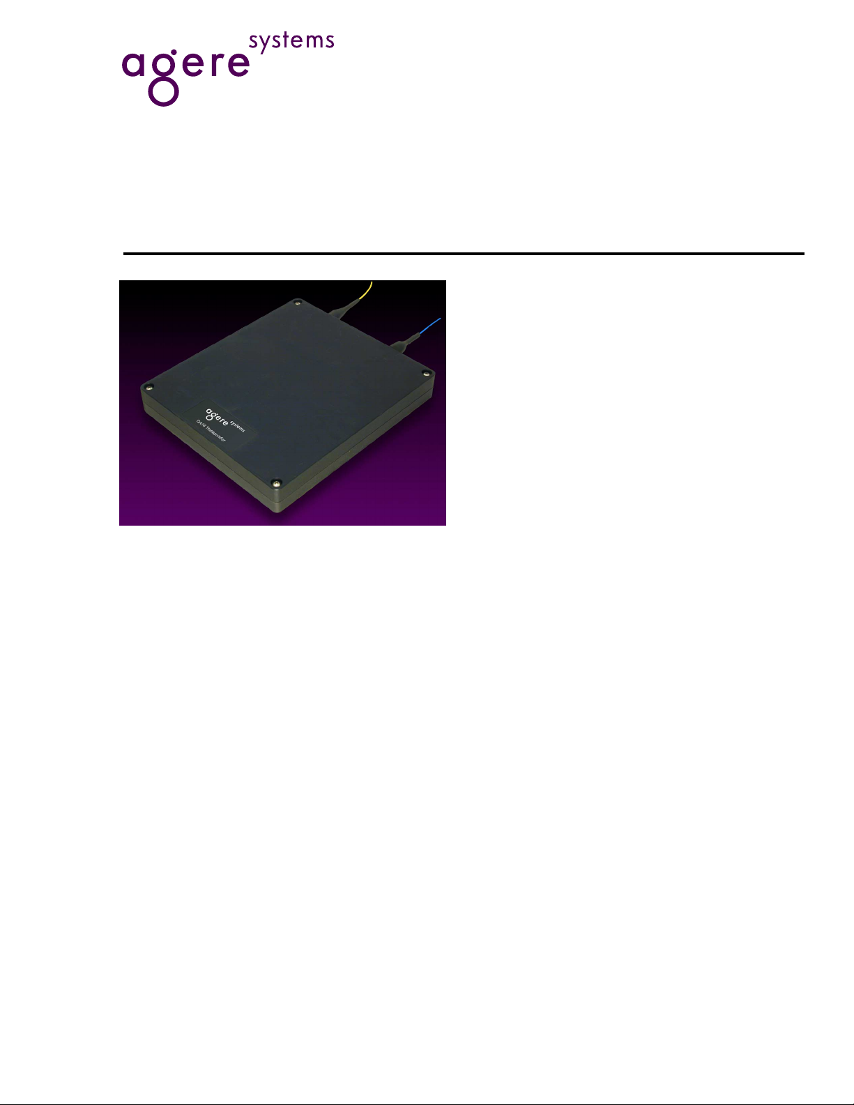
The CA16-type transponder s integrate up to 15 discre te
ICs and optical components, including a 2.5Gbits/s op-
tical transmitter and receiver pair, all in a single, compact packag e.
Features
2.5 Gbits/s optical transmitter and receiver with
■
16-channel 155 Mbits/s multiplexer/demultiplexer.
Available with 1.55 µm cooled DFB laser transmit-
■
ter and an APD receiver for long-reach applications:
— Offers 45 standard ITU wavelengths with
100 GHz spacing.
— Each module is capable of two wavelengths
under user control.
Pig ta iled, low- p r o file pack age.
■
Differential LVPECL data interface.
■
Operating case temperature range: 0 °C to 65 °C.
■
Automatic transmitter optical power control.
■
High-speed data communications
■
Description
The CA16-type transponder performs the parallel-toserial-to-optical transport and optical transport-toserial-to-parallel function of the section and photonic
layers of the SONET/SDH protocol. The CA16 transmitter se ctio n performs the bit ser i al i z a ti o n and op tical transmission of SONET/SDH OC-48/STM-16
data that has been formatted into standard SONET/
SDH compliant 16-bit parallel format. The CA16
receiver performs the optical-to-electrical conversion
function and is then able to detect frame and byte
boundaries and demultiplex the serial data into 16-bit
parallel OC-48/STM-16 format.
The CA16 transponder does not perform byte-level
multiplexing or interleaving.
Laser bias monitor outp ut.
■
Trans mitter laser disable input.
■
Line loopback and diagnostic loopback capability.
■

CA16-Type 2.5 Gbits/s DWDM Transponder with Advance Data Sheet
16-Chann el 155 Mb its/s Mu ltip lexer/Demu ltip le x er March 2001
Table of Contents
Contents Page Tables Page
Features ................................................................... 1
Applications .............................................................. 1
Description ............................................................... 1
Absolute Maximum Ratings...................................... 3
Block Diagram........................................................... 4
Pin Information ......................................................... 5
Pin Descriptions....................................................... 6
Functional Description .......... ................................. 12
Receiver ............................................................ 12
Transmitter ........................................................ 12
Loopback Modes............................................... 13
Transponder Interfacing..................................... 13
Optical Charac te r i stics ............................. ............ ..15
Electrical Characteristics ........................................ 16
Timing Characteristics........................................... 18
Transmitter Data Input Timing ........................... 18
Input Timing Mode 1 .......................................... 19
Input Timing Mode 2 .......................................... 20
Forward Clocking ...............................................21
PC
-to PICLK Timing........................................ 22
LK
PHERR/PHINIT.................................................. 2 3
Receiver Framing...............................................25
Wavelength Selection ............................................. 26
Qualification and Reliability .................................... 27
Laser Safety Information ....................................... 27
Class I Laser Product......................................... 27
Electromagnetic Em iss ions and Immunit y.......... 27
Outline Diagram ..................................................... 28
Ordering Information .............................................. 29
Related Product Information................................... 29
Table 1. CA16-Type Transponder Pinout .................6
Table 2. CA16-Type Transponder Input Pin
Descriptions...............................................10
Table 3. CA16-Type Transponder Output Pin
Descriptions ...............................................11
Table 4. OC-48/STM-1 6 Transmitter Optical
Characteristics .......................................... 15
Table 5. OC-48/STM-16 Receiver Optical
Characteristics .......................................... 15
Table 6. Power Supply Characteristics....................16
Table 7. Transmitter Electrical I/O Characteristics...16
Table 8. Receiver Electrical I/O Characteristics ......17
Table 9. Transmitter ac Timing Characteristics .......24
Table 10. Receiver ac Timing Characteristics .........24
Table 11. Ordering Information................................29
Table 12. Related Product Information ....................29
Figures Page
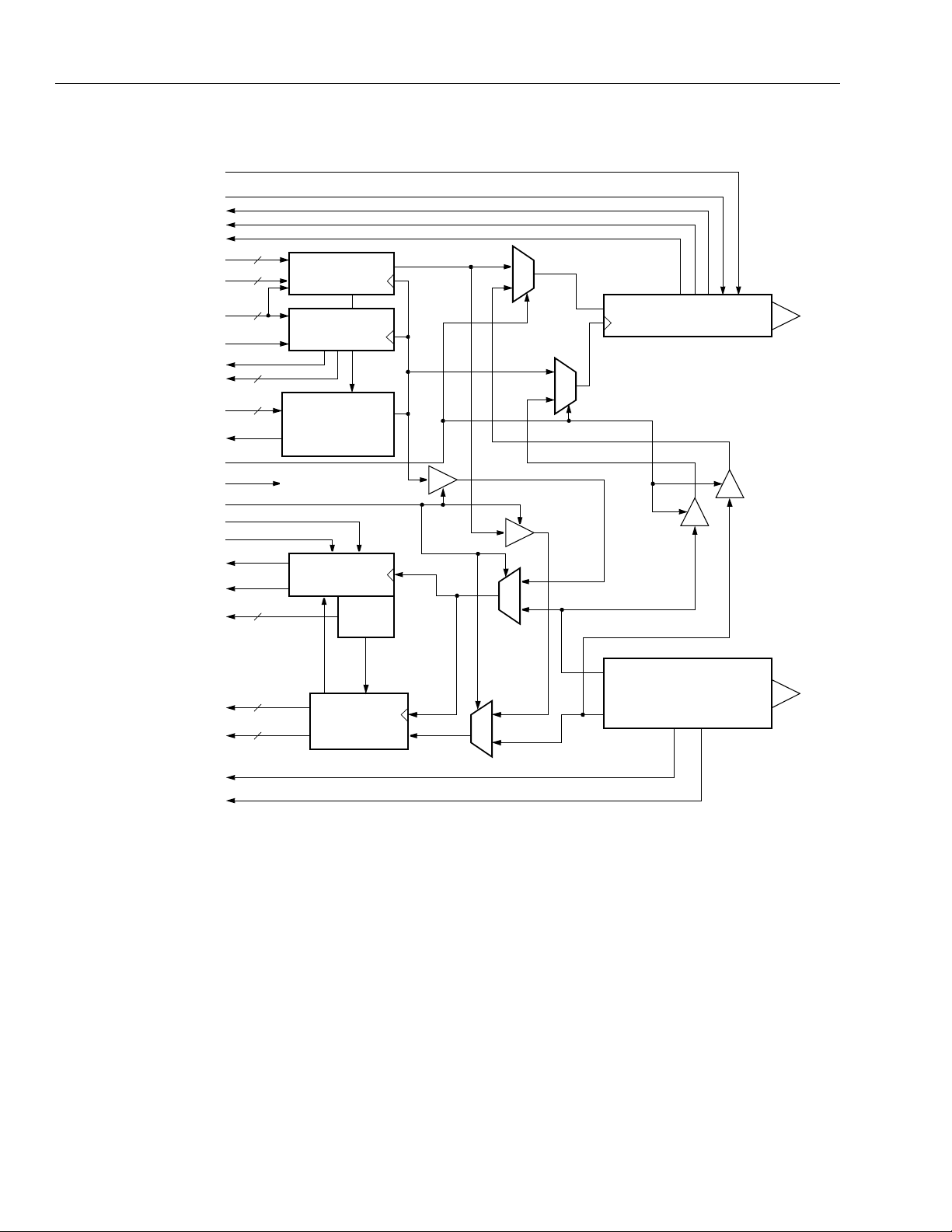
Figure 1. CA16-Type Tra nsponder Block Diagram ....4
Figure 2. CA16-Type Transponder Pinout.................5
Figure 3. Transponder Interfacing............................13
Figure 4. Interfacing to the T
Figure 5. Block Diagram Timing Mode 1..................19
Figure 6. Block Diagram Timing Mode 2..................20
Figure 7. Forward Clocking of the
CA16 Transponder ..................................21
Figure 8. PC
Figure 9. PHERR/PHINIT Timing. ........... .................23
Figure 10. ac Input Timing .......................................24
Figure 11. Receiver Output Timing Diagram ...........24
Figure 12. Frame and Byte Detection......................25
Figure 13. OOF Timing (FRAMEN = High)............ ..25
Figure 14. FRAME N Tim ing.................... ............ .....26
-to PICLK Timing...............................22
LK
XREFCLK
Input.............14
2
Agere Systems Inc..

Advance Data Sheet CA16-Type 2.5 Gbits/s DWDM Transponder with
March 2001 16-Channel 155 Mbits/s Multiplexer/Demultiplexer
Description
(continued)
Figure 1 shows a simplified block diagram of the CA16Type transponder. This device is a bidirectional module
designed to provide a SONET or S DH compliant electro-optical interface between the SONET/SDH photonic
physical layer and the electrical section layer. The module contains a wavelength-tunable (two channels at
100 GHz) 2.5 Gbits/s optical transmitter and a
2.5 Gbits/s optical receiver in the same physical package along with the electronics necessary to multiplex
and demultiplex sixteen 155 Mbits/s electrical channels.
Clock synthesis, clock recovery , and SONET/SDH
frame detection ci rcuits are also included within the
module.
In the transmit direction, the transponder module multiplexes sixteen 155 Mbits/s PECL electrical data signals
into an optical signal at 2488.32 Mbits/s for launching
into optical fiber. An internal 2.488 GHz reference oscillator is phase-locked to an external 155.52 MHz data
timing refe rence.
Absolute Maximum Ratings
The optical transmitter is available at any ITU grid
wavelength with a 1.55 µm cooled DFB laser for longreach applications. Th e optical outp u t signal is S ONET
and ITU compliant for OC-48/STM-16 applications as
shown in Table 4, OC-48/STM-1 6 Transmitter Optical
Characteristics.
In the receive direction, the transponder module
receives a 2488.32 Mbits/s optical signal and converts
it to an electrical signal, and then extracts a clock signal and demultiplexes the data into sixteen 155 Mbits/s
differential LV PECL data signals. When enabled, the
module can also detect SONET/SDH frame boundaries. The optical receiver is available with an APD
photodetector. The receiver operates over the wavelength range of 1.1 µm to 1.6 µm and is fully com pliant
to SONET/SDH OC-48/STM-16 physical layer specifications as shown in Table 5, OC-48/STM-16 Receiver
Optical Characteristics.
Stresses in excess of the absol ute maximum ratings can cause permanent damage to the dev ice. These are absolute stress ratin gs onl y. Function al operatio n of the device is not implied at thes e or any o ther conditions in excess
of those given in the operations sections of the data sheet. Exposure to absolute maximum ratings for extended
periods can adversely affect reliability.
Parameter Symbol Min Max Unit
Operating Case Temperature Range T
Storage Case Temperature Range T
C
S
075°C
–40 85 °C
Supply Voltage — –0.5 5.5 V
Voltage o n Any LV PECL P in — 0 V
CC
—
High-speed LVPECL Output Source Current — — 50 mA
Static Discharge Voltage
1
ESD — 500 V
Relative Humidity (noncondensing) RH — 85 %
Receiver Optical Input Power—Biased APD P
IN
—0dBm
Minimum Fiber Bend Radius — 1.25 (31.8) — in. (mm)
1. Human body model.
Agere Systems Inc.
3
CA16-Type 2.5 Gbits/s DWDM Transponder with Advance Data Sheet
16-Chann el 155 Mb its/s Mu ltip lexer/Demu ltip le x er March 2001
Block Diagram
WS (WAVELENGTH
SELECT)
TXDIS
WDEA
LSR ALRM
LPM
TXD[0:15]P
TXD[0:15]N
PICLKP/N
PHINIT
PHERR
PCLKP/N
TXREFCLKP/N
LOCKDET
LLOOP
RESET
DLOOP
OOF
FRAMEN
SEARCH
FP
POCLKP/N
16
16
2
2
2
CLOCK DIVIDER
PHASE DETECT
2
16:1 PARALLEL
TO SERIAL
TIMING
GENERATION
AND
FRAME/BYTE
DETECT
TIMING
GEN
MUX
D
OC-48/STM-16
OPTICAL TRANSMITTER
MUX
MUX
RXQ[0:15]P
RXQ[0:15]N
LOS
IPDMON
16
16
1:16 SERIAL
TO PARALLEL
MUX
Figure 1. CA16-Type Transponder Block Diagram
CK
OC-48/STM-16
OPTICAL RECEIVER
W/CLOCK RECOVERY
D
1-1011(F).f
4
Agere Systems Inc.
Advance Data Sheet CA16-Type 2.5 Gbits/s DWDM Transponder with
March 2001 16-Channel 155 Mbits/s Multiplexer/Demultiplexer
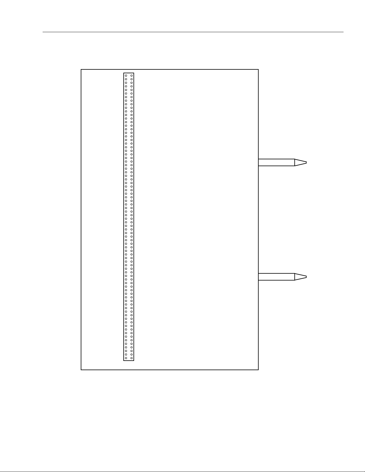
Pin Information
60
50
40
30
20
10
1
FGND
NC
NC
NC
NC
RXDGND
RXQ00N
RXQ00P
RXQ02N
RXQ02P
RXDGND
RXQ04N
RXQ04P
RXQ06N
RXQ06P
RXDGND
RXQ08N
RXQ08P
RXQ10N
RXQ10P
RXDGND
RXQ12N
RXQ12P
RXQ14N
RXQ14P
RXDGND
VTEC
VTEC
VTEC
RXDGND
RXAGND
RXAGND
RX3.3A
RXAGND
RXAGND
NC
RX3.3D
RX3.3D
RXDGND
FRAMEN
WDEA
DLOOP
NC
LSRBIAS
LSRALM
LPM
TXAGND
TX3.3A
TX3.3A
TXAGND
TX3.3D
TX3.3D
TXDGND
LOCKDET
PICLKN
PICLKP
TXDGND
TXD01N
TXD01P
TXD03N
TXD03P
TXDGND
TXD05N
TXD05P
TXD07N
TXD07P
TXDGND
TXD09N
TXD09P
TXD11N
TXD11P
TXDGND
TXD13N
TXD13P
TXD15N
TXD15P
TXDGND
IPDMON
FGND
FGND 16080
NC
NC
NC
NC
RXDGND
RXQ01N
RXQ01P
RXQ03N
RXQ03P
RXDGND 15070
RXQ05N
RXQ05P
RXQ07N
RXQ07P
RXDGND
RXQ09N
RXQ09P
RXQ11N
RXQ11P
RXDGND 140
RXQ13N
RXQ13P
RXQ15N
RXQ15P
RXDGND
VTEC
VTEC
WS
NC
POCLKN
POCLKP
RX3.3A
RXAGND
RXAGND
SEARCH
RX3.3D
RX3.3D
RXDGND
OOF
FP
RXDGND
LOS
LLOOP
PHERR
NC
TXDIS
PHINIT
NC
TX3.3A
TX3.3D
TXAGND
TXDGND
PCLKN
PCLKP
TXDGND
TXD00N
TXD00P
TXDGND
TXD02N
TXD02P
TXD04N
TXD04P
TXDGND
TXD06N
TXD06P
TXD08N
TXD08P
TXDGND
TXD10N
TXD10P
TXD12N
TXD12P
TXDGND
TXD14N
TXD14P
TXREFCLKN
TXREFCLKP
TXDGND
RESET
FGND
130
120
110
100
90
81
RX
TX
TOP VIEW
Agere Systems Inc.
1-1014(F).d
Figure 2. CA16-Type Transponder Pinout
5

CA16-Type 2.5 Gbits/s DWDM Transponder with Advance Data Sheet
16-Chann el 155 Mb its/s Mu ltip lexer/Demu ltip le x er March 2001
Pin Descriptions
Table 1. CA16-Type Transponder Pinout
Pin # Pin Name I/O Logic Description
01 FGND I Supply Frame Ground
02 IPDMON O Analog Receiver Photodiode Curren t Monitor
03 TxDGND I Supply Transmitter Digital Ground
04 TxD15P I LVPECL Trans mi tter 155 Mbits/s MSB Data Input
05 TxD15N I LVPECL Transmitter 155 Mbits/s MSB Data Input
06 TxD13P I LVPECL Transmitter 155 Mbits/s Data Input
07 TxD13N I LVPECL Transmitter 155 Mbits/s Data Input
08 TxDGND I Supply Transmitter Digital Ground
09 TxD11P I LVPECL Transmitter 155 Mbits/s Data Input
10 TxD11N I LVPECL Transmitter 155 Mbits/s Data Input
11 TxD09P I LVPECL Transmitter 155 Mbits/s Data Input
12 TxD09N I LVPECL Transmitter 155 Mbits/s Data Input
13 TxDGND I SUPPLY Transmitter Digital Ground
14 TxD07P I LVPECL Transmitter 155 Mbits/s Data Input
15 TxD07N I LVPECL Transmitter 155 Mbits/s Data Input
16 TxD05P I LVPECL Transmitter 155 Mbits/s Data Input
17 TxD05N I LVPECL Transmitter 155 Mbits/s Data Input
18 TxDGND I Supply Transmitter Digital Ground
19 TxD03P I LVPECL Transmitter 155 Mbits/s Data Input
20 TxD03N I LVPECL Transmitter 155 Mbits/s Data Input
21 TxD01P I LVPECL Transmitter 155 Mbits/s Data Input
22 TxD01N I LVPECL Transmitter 155 Mbits/s Data Input
23 TxDGND I Supply Transmitter Digital Ground
24 PIC
25 PIC
P I LVPECL Byte-Aligned Parallel Input Clock at 155 MHz
LK
N I LVPECL Byte-Aligned Parallel Input Clock at 155 MHz
LK
26 LOCKDET O LVTTL Lock Detect
27 TxDGND I Supply Transmitter Digital Ground
28 Tx3. 3D I Supply Trans mi tter 3.3 V Digital Supply
29 Tx3. 3D I Supply Trans mi tter 3.3 V Digital Supply
30 TxAGND I Supply Transmitter Analog Ground
31 Tx3.3A I Supply Transmitter 3.3 V Analog Supply
32 Tx3.3A I Supply Transmitter 3.3 V Analog Supply
33 TxAGND I Supply Transmitter Analog Ground
34 LPM O Analog Laser Power Monitor
35 LSRALM O 5 V CMOS Laser Degrade Alarm
36 LSRBIAS O Analog Not Implemented on the CA16-Type Transponder
37 NC — — No User Connection Permitted
38 D
LOOP
I LVTTL Diagnostic Loopback
39 WDEA O 5 V CMOS Wavelength Deviation Error Alarm
40 FP O LVPECL Frame Pulse
41 FRAMEN I LVTTL Frame Enable
1. Frame ground is connected to the housing and is isolated from all circu it grounds (TxDGND, TxAGND, RxDGND, RxAGND).
2. Pins labeled no connec t i on must rem ain open c i rc uits; they have internal voltages and must not be con nected to V
or any signal node.
1
2
CC
, Grou nd,
6
Agere Systems Inc.

Advance Data Sheet CA16-Type 2.5 Gbits/s DWDM Transponder with
March 2001 16-Channel 155 Mbits/s Multiplexer/Demultiplexer
Pin Descriptions
(continued)
Table 1. CA16-Type Transponder Pinout (continued)
Pin # Pin Name I/O Logic Description
42 RxDGND I Supply Receiver Digital Ground
43 Rx3.3D I Supply Receiver 3.3 V Digital Supply
44 Rx3.3D I Supply Receiver 3.3 V Digital Supply
45 NC — — No User Connection Permitted
2
46 RxAGND I Supply Receiver Analog Ground
47 RxAGND I Supply Receiver Analog Ground
48 Rx3.3A I Supply Receiver 3.3 V Analog Supply
49 RxAGND I Supply Receiver Analog Ground
50 RxAGND I Supply Receiver Analog Ground
51 RxDGND I Supply Receiver Digital Ground
52 VTEC I Supply TEC Cooler 3 V Anal og Supply V ol ta ge
53 VTEC I Supply TEC Cooler 3 V Anal og Supply V ol ta ge
54 VTEC I Supply TEC Cooler 3 V Anal og Supply V ol ta ge
55 RxDGND I Supply Receiver Digital Ground
56 RxQ14P O LV PECL Receiver 155 M b i ts/s Data Output
57 RxQ14N O LVPECL Receiver 155 Mbits/s Data Output
58 RxQ12P O LV PECL Receiver 155 M b i ts/s Data Output
59 RxQ12N O LVPECL Receiver 155 Mbits/s Data Output
60 RxDGND I Supply Receiver Digital Ground
61 RxQ10P O LV PECL Receiver 155 M b i ts/s Data Output
62 RxQ10N O LVPECL Receiver 155 Mbits/s Data Output
63 RxQ08P O LV PECL Receiver 155 M b i ts/s Data Output
64 RxQ08N O LVPECL Receiver 155 Mbits/s Data Output
65 RxDGND I SUPPLY Receiver Digital Ground
66 RxQ06P O LV PECL Receiver 155 M b i ts/s Data Output
67 RxQ06N O LVPECL Receiver 155 Mbits/s Data Output
68 RxQ04P O LV PECL Receiver 155 M b i ts/s Data Output
69 RxQ04N O LVPECL Receiver 155 Mbits/s Data Output
70 RxDGND I Supply Receiver Digital Ground
71 RxQ02P O LV PECL Receiver 155 M b i ts/s Data Output
72 RxQ02N O LVPECL Receiver 155 Mbits/s Data Output
73 RxQ00P O LVPECL Receiver 155 Mbits/s LSB Data Output
74 RxQ00N O LVPECL Receiver 155 Mbits/s LSB Data Output
75 RxDGND I Supply Receiver Digital Ground
76 NC — — No User Connection Permitted
77 NC — — No User Connection Permitted
78 NC — — No User Connection Permitted
79 NC — — No User Connection Permitted
80 FGND I Supply Frame Ground
81 FGND I Supply Frame Ground
1
1
2
2
2
2
82 Reset I — Master Reset
1. Frame ground is connected to the housing and is isolated from all circuit grounds (TxDGND, TxAGND, RxDGND, RxAGND).
2. Pin s lab eled no c onnection must remain open circuits; they have internal voltages and must not be connected to V
or any signal node.
CC
, Grou nd,
Agere Systems Inc.
7

CA16-Type 2.5 Gbits/s DWDM Transponder with Advance Data Sheet
16-Chann el 155 Mb its/s Mu ltip lexer/Demu ltip le x er March 2001
Pin Descriptions
(continued)
Table 1. CA16-Type Transponder Pinout (continued)
Pin # Pin Name I/O Logic Description
83 TxDGND I Supply Transmitter Digital Ground
84 TxR
85 TxR
P I LVPECL T ransmitter 155 Mbits/s Reference Clock Input
EFCLK
N I LVPECL Transmitter 155 Mbits/s Reference Clock Input
EFCLK
86 TxD14P I LVPECL Transmitter 155 Mbits/s Data Input
87 TxD14N I LVPECL Transmitter 155 Mbits/s Data Input
88 TxDGND I Supply Transmitter Digital Ground
89 TxD12P I LVPECL Transmitter 155 Mbits/s Data Input
90 TxD12N I LVPECL Transmitter 155 Mbits/s Data Input
91 TxD10P I LVPECL Transmitter 155 Mbits/s Data Input
92 TxD10N I LVPECL Transmitter 155 Mbits/s Data Input
93 TxDGND I SUPPLY Transmitter Digital Ground
94 TxD08P I LVPECL Transmitter 155 Mbits/s Data Input
95 TxD08N I LVPECL Transmitter 155 Mbits/s Data Input
96 TxD06P I LVPECL Transmitter 155 Mbits/s Data Input
97 TxD06N I LVPECL Transmitter 155 Mbits/s Data Input
98 TxDGND I Supply Transmitter Digital Ground
99 TxD04P I LVPECL Transmitter 155 Mbits/s Data Input
100 TxD04N I LVPECL Transmitter 155 Mbits/s Data Input
101 TxD02P I LVPECL Transmitter 155 Mbits/s Data Input
102 TxD02N I LVPECL Transmitter 155 Mbits/s Data Input
103 TxDGND I SUPPLY Transmitter Digital Ground
104 TxD00P I LVPECL Transmitter 155 Mbits/s LS B Data Input
105 TxD00N I LVPECL Transmitter 155 Mbits/s LSB Data Input
106 TxDGND I Supp ly Transmitter Digital Ground
107 PC
108 PC
P O LVPECL Transmitter Parallel Reference Clock Output
LK
N I LVPECL Transmitter Parallel Reference Clock Output
LK
109 TxDGND I Supp ly Transmitter Digital Ground
110 TxAGND I Supply Transmitter Analog Ground
111 Tx3.3D I Supply Transmitter Digital 3.3 V Supply
112 Tx3.3A I Supply T r ansmitter Analog 3.3 V Supply
113 NC — — Future Function (I
2
C Clock)
114 PHINIT I LVPECL Phase Initialization
115 T
116 NC — — Future Function (I
DIS I TTL Transmitter Di sable
X
2
C Data)
117 PHERR O L VPECL Phase Error
118 L
LOOP
I LVTTL Line Loopback (active-low)
119 LOS O LVTTL Loss of Sign al
120 RxDGND I Supply Receiver Digital Ground
121 OOF I LVTT L Out of Frame (enable frame detection)
122 RxDGND I Supply Receiver Digital Ground
123 Rx3.3D I Supp ly Receiver Digital 3.3 V Supply
1. Frame ground is connected to the housing and is isolated from al l cir cu it g rounds (TxDGND, TxAGND, RxDGND, RxAGND).
2. Pins labeled no connec t i on must rema in open circui ts; they have internal voltages and must not be con nected to V
or any signal node.
CC
, Grou nd,
8
Agere Systems Inc.

Advance Data Sheet CA16-Type 2.5 Gbits/s DWDM Transponder with
March 2001 16-Channel 155 Mbits/s Multiplexer/Demultiplexer
Pin Descriptions
(continued)
Table 1. CA16-Type Transponder Pinout (continued)
Pin # Pin Name I/O Logic Description
124 Rx3.3D I SUPPLY Receiver Digital 3.3 V Supply
125 SE ARCH O LVTTL Frame Search Output
126 RxAGND I Supply Receiver Analog G r ound
127 RxAGND I Supply Receiver Analog G r ound
128 Rx3.3A I Supply Receiver Analog 3.3 V Supply
129 POC
130 POC
131 NC — — No User Connection Permitted
P O LV PECL Byte-Aligned Parallel Output Clock at 155 MHz
LK
N O LVPECL Byte-Aligned Parallel Output Clock at 155 MHz
LK
2
132 WS I L VTTL Binary Input to Select One of Two Grid Wavelengths
133 VTEC I Supply TEC Cooler 3 V Analog Supply Vol tage
134 VTEC I Supply TEC Cooler 3 V Analog Supply Vol tage
135 RxDGND I Supply Receiver Digital Ground
136 RxQ15P O LVPECL Receiver MSB 155 Mbits/s Data Output
137 RxQ15N O LVPECL Receiver MSB 155 Mbits/s Data Output
138 RxQ13P O LVPECL Receiver 155 Mbits/s Data Output
139 RxQ13N O LVPECL Receiver 155 Mbits/s Data Output
140 RxDGND I Supply Receiver Digital Ground
141 RxQ11P O LVPECL Receiver 155 Mbits/s Data Output
142 RxQ11N O LVPECL Receiver 155 Mbits/s Data Output
143 RxQ09P O LVPECL Receiver 155 Mbits/s Data Output
144 RxQ09N O LVPECL Receiver 155 Mbits/s Data Output
145 RxDGND I Supply Receiver Digital Ground
146 RxQ07P O LVPECL Receiver 155 Mbits/s Data Output
147 RxQ07N O LVPECL Receiver 155 Mbits/s Data Output
148 RxQ05P O LVPECL Receiver 155 Mbits/s Data Output
149 RxQ05N O LVPECL Receiver 155 Mbits/s Data Output
150 RxDGND I Supply Receiver Digital Ground
151 RxQ03P O LVPECL Receiver 155 Mbits/s Data Output
152 RxQ03N O LVPECL Receiver 155 Mbits/s Data Output
153 RxQ01P O LVPECL Receiver 155 Mbits/s Data Output
154 RxQ01N O LVPECL Receiver 155 Mbits/s Data Output
155 RxDGND I Supply Receiver Digital Ground
156 NC — — No User Connection Permitted
157 NC — — No User Connection Permitted
158 NC — — No User Connection Permitted
159 NC — — No User Connection Permitted
160 FGND I Supply Frame Ground
1. Frame ground is connected to the housing and is isolated from all circuit grounds (TxDGND, TxAGND, RxDGND, RxAGND).
2. Pins labeled no connection must remain open circuits; they have internal voltages and must not be connected to V
node.
1
2
2
2
2
CC
, Ground, or any signa l
Agere Systems Inc.
9
 Loading...