

AGERE BTF1A16G Datasheet

Dual Differential Transceiver BTF1A
With Idle Bus Indicator
■
Features
Driver Features
■
Produces a logic zero in third state
■
400 mV difference voltage in third state
■
Two line drivers per package
■
Logic to convert TTL input logic levels to differential, pseudo-emmiter coupled logic (ECL) output
logic levels
■
No line loading when VCC = 0 V
■
High output driver for 50 Ω loads
■
200 mA short-circuit current (typical)
■
2.0 ns maximum propagation delay
■
<0.2 ns output skew (typical)
Receiver Features
■
Two line receivers per package
■
High input impedance ≅ 8 kΩ
■
Logic that converts differential input logic levels to
TTL output logic levels
■
4.0 ns maximum propagation delay
■
<0.20 V input sensitivity (typical)
−1.2 V to +7.2 V common-mode range
■
Common Device Features
■
Common enable for each driver/receiver pair
■
Operating temperature range: –40 °C to +125 °C
(wider than the 41 Series)
Electrostatic discharge (ESD) performance better
than the 41 Series
■
Lower power requirement than the 41 Series
Description
The BTF1A device is a dual differential transceiver
circuit that transmits and receives digital data over
balanced transmission lines and is compatible with
Lucent Technologies Microelectronics Group differential drivers and receivers. It is designed to provide
a strong logic zero when in the third state. The minimum difference voltage in the third state is 400 mV. It
is designed specifically for bus applications where a
well-defined logic state is needed when the bus is
idle. The driver puts out a logic
state mode, which is easily overriden by an active
buffer on the bus. When all the buffers on the bus are
inactive (third state), the signal on the bus is a
indicating that the bus is idle.
The dual drivers translate input TTL logic levels to differential pseudo-ECL output levels. The dual receiver
converts differential input logic levels to TTL output
levels. Each driver/receiver pair has its own common
enable control allowing serial data and a control clock
to be transmitted and received on a single integrated
circuit. The BTF1A tr ansceiv er re quires the customer
to supply termination resistors on the circuit board.
The powerdown loading characteristics of the
receiver input circuit are approximately 8 kΩ relative
to the power supplies; hence, it will not load the
transmission line when the circuit is powered down.
For those circuits with termination resistors, the line
will remain impedance matched when the circuit is
powered down. The driver does not load the line
when it is powered down.
Data Sheet
March 2001
when in the third
zero
zero
■
Single 5.0 V ± 5% supply
■
400 Mbits/s maximum data rate
■
Meets enhanced small device interface (ESDI)
standards
Dual Differential Transceiver BTF1A
With Idle Bus Indicator
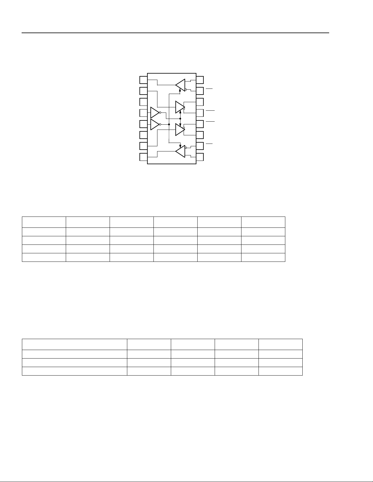
Pin Information
Data Sheet
March 2001
RO1
DI1
V
ED
ER
GND
DI2
RO2
1
2
CC
3
4
5
6
7
8
R1
D1
D2
R2
BTF1A
RI1
16
RI1
15
DO1
14
DO1
13
DO2
12
DO2
11
RI2
10
RI2
9
Figure 1. Differential Transceiver Logic Diagram
Table 1. Enable Truth Table
ED ER D1 D2 R1 R2
0 0 Active Active Active Active
1 0 Disabled Disabled Active Active
0 1 Active Active Disabled Disabled
1 1 Disabled Disabled Disabled Disabled
12-2747.a(F)
Absolute Maximum Ratings
Stresses in excess of the absolute maximum ratings can cause permanent damage to the device. These are absolute stress ratings only. Functional operation of the device is not implied at these or any other conditions in excess
of those given in the operational sections of the data sheet. Exposure to absolute maximum ratings for extended
periods can adversely affect device reliability.
Table 2. Absolute Maximum Ratings
Parameter Symbol Min Max Unit
Power Supply Voltage V
Ambient Operating Temperature T
Storage Temperature T
CC
A
stg
—6.5V
−40 125 °C
−55 150 °C
2 Agere Systems Inc.

Data Sheet
March 2001
Dual Differential Transceiver BTF1A
With Idle Bus Indicator
Electrical Characteristics
For variations in electrical characteristics over the temperature range, see Figure 10 through Figure 12.
Table 3. Power Supply Current Characteristics
A
= −40 °C to +125 °C, V
T
CC
= 5 V ± 0.25 V.
Parameter Symbol Min Typ Max Unit
Power Supply Current (V
All Outputs Disabled
All Outputs Enabled
CC
= 5.5 V)
I
I
CC
CC
—
—
40
20
65
35
mA
mA
Third State
The BTF1A driver produces pseudo-ECL levels, and has a third-state mode, which is different than a conventional
TTL device. When a driver is placed in the third state, the base of the output transistors are pulled low, bringing the
outputs below the active-low level. The BTF1A is unique because it provides a logic zero at its output when in the
third state. If all the buffers on the bus are in the third state, the BTF1A is designed to deliver a logic zero to the bus
to act as an indicator that the bus is idle. The guaranteed zero level, Vdo
– Vdo, is 0.4 V.
Agere Systems Inc. 3

Dual Differential Transceiver BTF1A
With Idle Bus Indicator
Data Sheet
March 2001
Electrical Characteristics
(continued)
Table 4. Driver Voltage and Current Characteristics
A
For variations in output voltage over the temperature range, see Figure 10 and Figure 11. T
= −40 °C to +125 °C.
Parameter Symbol Min Typ Max Unit
Output Voltages:
1
Low
1
High
:V
Differential Voltage (V
OH
– VOL)V
V
DIFF
OL
OH
OH –
V
1.4 V
CC
− 1.8 V
V
OH
− 1.1 V
CC
− 1V
OH
− 0.65 V
CC
− 0.8 V
0.65 1.1 1.4 V
Output Voltage Third State:
Difference Voltage Vdo
Third State, I
Output Voltages (T
1
Low
1
High
:V
OH
= –1.0 mA, VCC = 4.75 V V
A
Differential Voltage (V
- Vdo V
= 0 °C to 85 °C):
OH
– VOL)V
DIFZ
V
DIFF
OZ
OL
OH
0.4 0.6 — V
OL
——V
OH –
V
1.4 V
CC
− 1.5 V
V
OH
− 1.1 V
CC
− 1V
− 0.2 V
OH
− 0.8 V
CC
− 0.8 V
0.8 1.1 1.4 V
Input Voltages:
IH
OS
IH
IH
2
IL
3
IL
3
IL
2
IK
——0.8V
——0.8V
——0.7V
2.0 — — V
——−1.0 V
–100 — — mA
IL
——−400 µA
——20 µA
— — 100 µA
CC
Low, V
= 5.25 V: V
Data Input V
Enable Input V
High, V
Clamp, V
Short-circuit Output Current, V
Input Currents, V
Low, V
High, V
Reverse, V
1. Values are with terminations as per Figure 7.
2. The input levels and diff erence voltage provide zero noise immunity and should be tested only in a static, noise-free environment.
3. Test must be performed one lead at a time to prevent damage to the devi ce .
CC
= 4.75 V V
CC
= 4.75 V, II = –5.0 mA V
CC
= 5.25 V I
CC
= 5.25 V:
I
= 0.4 V I
I
= 2.7 V I
I
= 5.25 V I
4 Agere Systems Inc.

Data Sheet
March 2001
Dual Differential Transceiver BTF1A
With Idle Bus Indicator
Electrical Characteristics
(continued)
Table 5. Receiver Voltage and Current Characteristics
OH
For variation in minimum V
and maximum VOL over the temperature range, see Figure 10. TA = –40 °C to +125 °C.
Parameter Symbol Min Typ Max Unit
CC
Output Voltages V
OL
Low, I
High, I
= 8.0 mA
OH
= −400 µA V
= 4.75 V:
1
OL
V
OH
——0.5V
2.4 — — V
Enable Input Voltages:
CC
Low, V
High, V
Clamp, V
Minimum Differential Input Voltages, V
−0.80 V < V
= 5.25 V V
CC
= 4.75 V V
CC
= 4.75 V, II = –5.0 mA V
IH – VIL
IH
< 7.2 V, −1.2 V < VIL < 6.8 V V
2
:
Input Offset Voltage V
Output Currents, V
Off-state (high Z), V
Off-state (high Z), V
CC
= 5.25 V:
O
= 0.4 V I
O
= 2.4 V I
Short Circuit I
Enable Input Currents, V
IN
Low, V
High, V
Reverse, V
= 0.4 V I
IN
= 2.7 V I
IN
= 5.5 V I
CC
= 5.25 V:
IL
IH
IK
TH
OFF
OZL
OZH
OS
IL
IH
IH
1
1
——0.7V
2.0 — — V
——−1.0 V
1
—0.10.20V
0.03 0.05 V
——–20µA
——20µA
3
–25 — –100 mA
— — –400 µA
——20µA
——100µA
Differential Input Currents:
IN
Low, V
High, V
1. The input levels and difference voltage provide zero noise immunity and should be tested only in a static, noise-free environment.
2. Outputs of unused receivers assume a logic 1 level when the inputs are left open. (It is recommended that all unused positive inputs
be tied to the positive power supply. No external series resistor is required.)
3. Test must be performed one lead at a time to prevent damage to the device.
= –1.2 V I
IN
= 7.2 V I
IL
IH
——−1.0 mA
——1.0mA
Agere Systems Inc. 5
 Loading...