

AGERE BRT1A16P, BRT1A16NB, BRT1A16G, BRT1A16E, BRR1A16P Datasheet
...
Quad Differential Receivers
BRF1A, BRF2A, BRS2B, BRR1A, and BRT1A
Data Sheet
April 2001
Features
■
Pin equivalent to the general-trade 26LS32 device,
with improved speed, reduced power consumption,
and significantly lower levels of EMI
■
High input impedance approximately 8 kΩ
■
Four line receivers per package
■
400 Mbits/s maximum data rate when used with
Agere Systems Inc. data transmission drivers
■
Meets enhanced small device interface (ESDI)
standards
■
4.0 ns maximum propagation delay
■
<0.20 V input sensitivity
■ −1.2 V to +7.2 V common-mode range
■ −40 °C to +125 °C ambient operating temperature
range (wider than the 41 Series)
■
Single 5.0 V ± 10% supply
■
Output defaults to logic 1 when inputs are left
open*
■
Available in four package types
■
Lower power requirement than the 41 Series
Description
These quad differential receivers accept digital data
over balanced transmission lines. They translate
differential input logic levels to TTL output logic
levels. All devices in this family have four receivers
with a common enable control. These receivers are
pin equivalent to the general-trade 26LS32, but offer
increased speed and decreased power consumption.
They replace the Agere 41 Series receivers.
* This feature is available on BRF1A and BRF2A.
The BRF1A device is the generic receiver in this
family and requires the user to supply external
resistors on the circuit board for impedance
matching.
The BRF2A is identical to the BRF1A, but has an
electrostatic discharge (ESD) protection circuit
added to significantly improve the ESD human-body
model (HBM) characteristics on the differential input
terminals.
The BRS2B is identical to the BRF2A, but has a
preferred state feature that places the output in the
high state when the inputs are open, shorted to
ground, or shorted to the power supply.
The BRR1A is equivalent to the BRF1A, but has a
110 Ω resistor connected across the differential
inputs. This eliminates the need for an external
resistor when terminating a 100 Ω impedance line.
This device is designed to work with the DP1A or
PNPA in point-to-point applications.
The BRT1A is equivalent to the BRF1A; however, it
is provided with a Y-type resistor network across the
differential inputs and terminated to ground. The
Y-type termination provides the best EMI results.
This device is not recommended for applications
where the differences in ground voltage between the
driver and the receiver exceed 1 V. This device is
designed to work with the DG1A or PNGA in point-topoint applications.
The powerdown loading characteristics of the
receiver input circuit are approximately 8 kΩ relative
to the power supplies; hence, they will not load the
transmission line when the circuit is powered down.
For those circuits with termination resistors, the line
will remain impedance matched when the circuit is
powered down.
The packaging options that are available for these
quad differential line drivers include a 16-pin DIP; a
16-pin, J-lead SOJ; a 16-pin, gull-wing small-outline
integrated circuit (SOIC); and a 16-pin, narrow-body,
gull-wing SOIC.
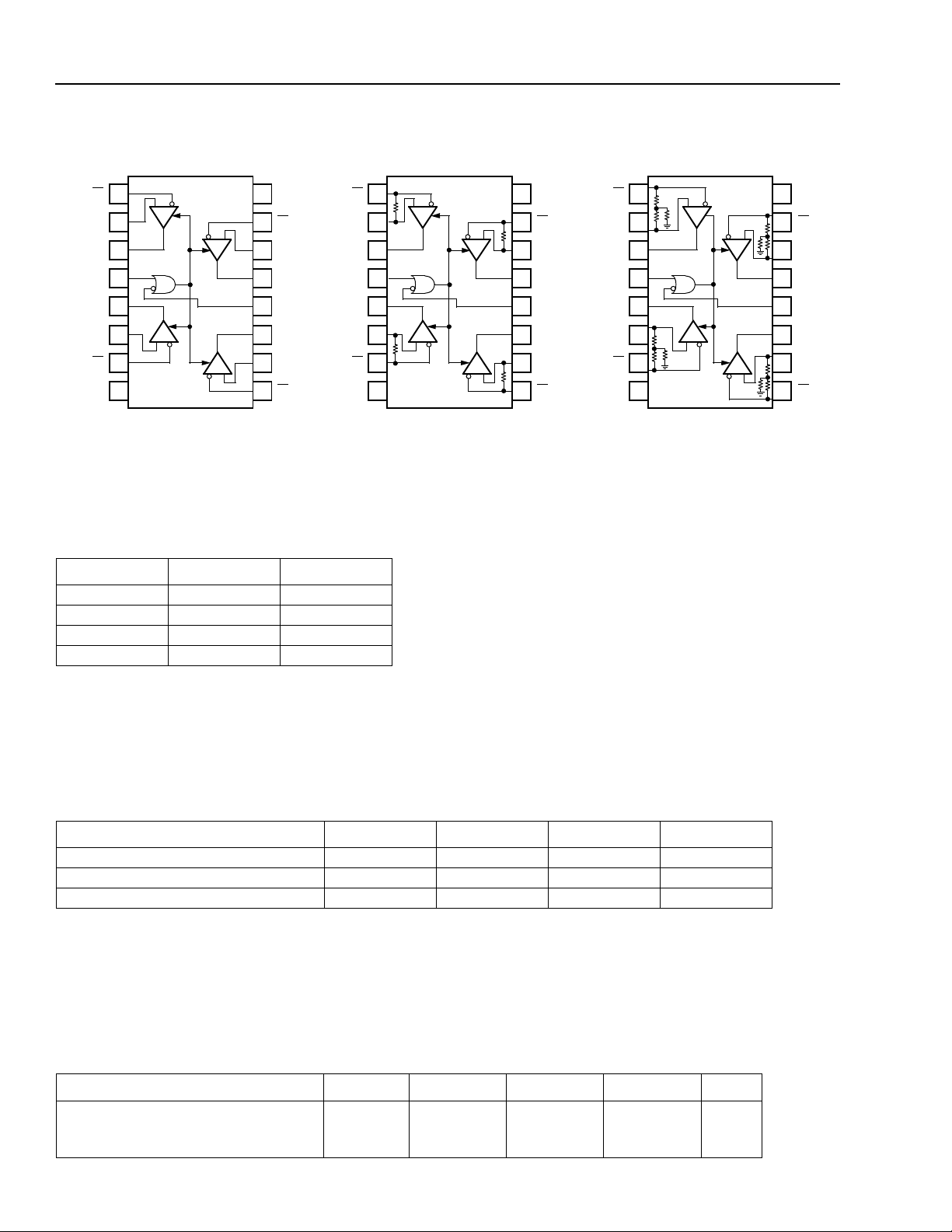
Quad Differential Receivers
BRF1A, BRF2A, BRS2B, BRR1A, and BRT1A
Pin Information
Data Sheet
April 2001
AI
1
AI
AO
E1
BO
BI
BI
GND
A
2
BRF1A
BRF2A
BRS2B
D
C
3
4
5
B
6
7
8
Table 1. Enable Truth Table
E1 E2 Condition
00Active
10Active
01Disabled
11Active
V
CC
16
DI
15
DI
14
DO
13
E2
12
CO
11
CI
10
CI
9
AO
E1
BO
GND
AI
1
AI
BI
BI
A
2
3
4
5
B
6
7
8
D
C
BRR1A BRT1A
V
CC
16
DI
15
DI
14
DO
13
E2
12
CO
11
CI
10
CI
9
AI
AI
AO
E1
BO
BI
BI
GND
Figure 1. Quad Differential Receiver Logic Diagrams
V
1
2
3
4
5
6
7
8
A
D
B
C
CC
16
DI
15
DI
14
DO
13
E2
12
CO
11
CI
10
CI
9
12-2281.a(F)
Absolute Maximum Ratings
Stresses in excess of the absolute maximum ratings can cause permanent damage to the device. These are
absolute stress ratings only. Functional operation of the device is not implied at these or any other conditions in
excess of those given in the operational sections of the data sheet. Exposure to absolute maximum ratings for
extended periods can adversely affect device reliability.
Parameter Symbol Min Max Unit
Power Supply Voltage V
Ambient Operating Temperature T
Storage Temperature T
CC
A
stg
—6.5V
−40 125 °C
−40 150 °C
Electrical Characteristics
For electrical characteristics over the temperature range, see Figure 7 through Figure 10.
Table 2. P ower Supply Current Characteristics
CC
See Figure 7 for variati on in I
over the temperature range. T
Parameter Symbol Min Typ Max Unit
Power Supply Current (V
All Outputs Disabled
All Outputs Enabled
CC
= 5.5 V):
CC
I
CC
I
2 Agere Systems Inc.
A
= –40 °C to +125 °C, V
30
20
CC
= 5 V ± 0.5 V.
45
32
mA
mA

Data Sheet
April 2001
Quad Differential Receivers
BRF1A, BRF2A, BRS2B, BRR1A, and BRT1A
Electrical Characteristics
(continued)
Table 3. Voltage and Current Characteristics
For variation in minim um V
OH
and maximum VOL over the temperature range, see Figure 8. T
A
= –40 °C to +125 °C.
Parameter Sym Min Typ Max Unit
Output Voltages, V
OL
Low, I
High, I
= 8.0 mA V
OH
= −400 µA V
CC
= 4.5 V:
OL
OH
——0.5V
2.4 — — V
Enable Input Voltages:
CC
Low, V
High, V
Clamp, V
Differential Input Voltages, V
−0.80 V < V
= 5.5 V V
CC
= 5.5 V V
CC
= 4.5 V, II = –5.0 mA V
2
IH – VIL
:
IH
< 7.2 V, −1.2 V < VIL < 6.8 V V
Input Offset Voltage V
Input Offset Voltage BRS2B V
Output Currents, V
Off-state (high Z), V
Off-state (high Z), V
CC
= 5.5 V:
O
= 0.4 V I
O
= 2.4 V I
Short Circuit I
Enable Currents , V
IN
Low, V
High, V
= 0.4 V I
IN
= 2.7 V I
Reverse, V
Differential Input Currents, V
IN
Low, V
High, V
= –1.2 V I
IN
= 7.2 V I
CC
= 5.5 V:
IN
= 5.5 V I
CC
= 5.5 V:
IL
IH
IK
TH
OFF
OFF
OZL
OZH
OS
IL
IH
IH
IL
IH
1
1
——0.7V
2.0 — — V
——–1.0V
1
—0.10.20V
0.02 0.05 V
0.1 0.15 V
——–20µA
——20µA
3
–25 — –100 mA
— — –400 µA
——20µA
——100µA
——−1.0 mA
——1.0mA
Differential Input Impedance (BRR1A):
Connected Between RI and RI
Differential Input Impedance (BRT1A)
1. The input levels and difference voltage provide zero noise immunity and should be tested only in a static, noise-free environment.
2. Outputs of unused receivers assume a logic 1 level when the inputs are left open. (It is recommended that all unused positive inputs
be tied to the positive power supply. No external series resistor is required.)
3. Test must be performed one lead at a time to prevent damage to the device.
4. See Figure 2.
4
O
R
1
R
2
R
— 110 — Ω
—60—Ω
—90—Ω
R1 R1
RI
R2
RI
12-2819.a(F)
Figure 2. BRT1A Terminating Resistor Configuration
Agere Systems Inc. 3
Quad Differential Receivers
BRF1A, BRF2A, BRS2B, BRR1A, and BRT1A
Timing Characteristics
Data Sheet
April 2001
Table 4. Timing Characteristics
For propagation delays (t
PLH
(See Figure 4 and Figure 5.)
PHL
and t
) over the temperature range, see Figure 9 and Figure 10.
Propagation delay test circuit connected to output is shown in Figure 6.
A
T
= –40 °C to +125 °C, V
CC
= 5 V ± 0.5 V.
Parameter Symbol Min Typ Max Unit
Propagation Delay:
Input to Output High t
Input to Output Low t
Disable Time, C
L
= 5 pF:
High-to-high Impedance t
Low-to-high Impedance t
PLH
PHL
PHZ
PLZ
1.5 2.5 4.0 ns
1.5 2.5 4.0 ns
—512ns
—512ns
Pulse Width Distortion, ltpHL − tpLHI:
Load Capacitance (C
Load Capacitance (C
L
) = 15 pF tskew1 — — 0.7 ns
L
) = 150 pF tskew1 — — 4.0 ns
Output Waveform Skews:
Part-to-Part Skew, T
Part-to-Part Skew, T
A
= 75 °C ∆tskew1p-p — 0.8 1.4 ns
A
= –40 °C to +125 °C ∆tskew1p-p — — 1.5 ns
Same Part Skew ∆tskew — — 0.3 ns
Enable Time:
High Impedance to High t
High Impedance to Low t
Rise Time (20%—80%) t
Fall Time (80%—20%) t
PZH
PZL
tLH
tHL
—812ns
—812ns
——3.0ns
——3.0ns
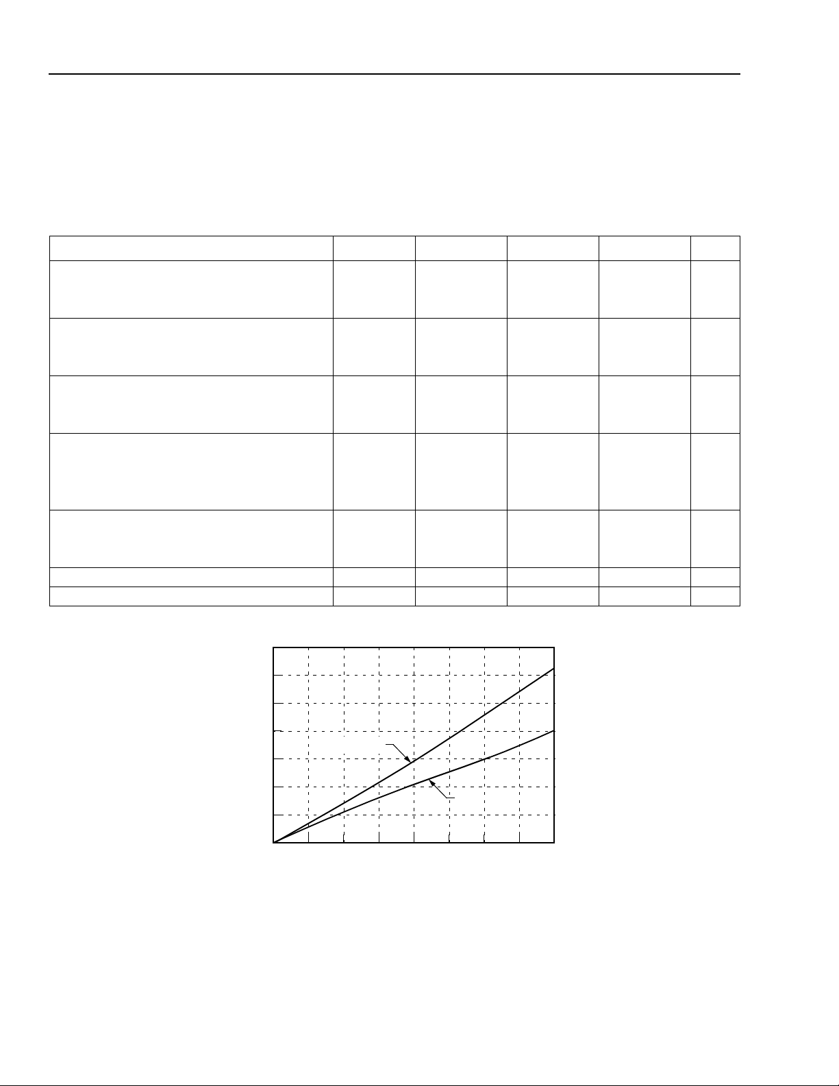
7
(ns)
P
6
5
4
3
2
1
0
EXTRINSIC PROPAGATION DELAY, t
Note: This graph is included as an aid to the system designers. Total circuit delay varies with load capacitance. The total delay is the sum of the
delay due to the external capacitance and the intrinsic delay of the device.
PLH
t
(TYP)
PHL
t
(TYP)
25 50 75 100 125 150
LOAD CAPACITANCE, C
L
(pF)
175 2000
12-3462(F)
Figure 3. T ypical Extrinsic Propagation Delay vs. Load Capacitance at 25 °C
4 Agere Systems Inc.
 Loading...