

AGERE BPPGA16P, BPPGA16G, BPPGA16E, BPNPA16P, BPNPA16G Datasheet
...
Data Sheet
January 1999
Quad Differential Drivers
BDG1A, BDP1A, BDGLA, BPNGA, BPNPA, and BPPGA
Features
Pin-equivalent to the general-trade 26LS31 device,
■
with improved speed, reduced power consumption,
and significantly lower levels of EMI
Four line drivers per package
■
Meets ESDI standards
■
2.0 ns maximum propagation delay
■
Single 5.0 V ± 10% supply
■
Operating temperature range: −40 °C to +125 °C
■
(wider than the 41 Series)
400 Mbits/s maximum data rate
■
Logic to convert TTL input logic levels to differen-
■
tial, pseudo-ECL output logic levels
No line loading when VCC = 0 (BDG1A, BDP1A
■
only)
High output driver for 50 Ω loads
■
<0.2 ns output skew (typical)
■
On-chip 220 Ω loads available
■
Third-state outputs available
■
Surge-protection to ±60 V for 10 ms available
■
(BPNGA, BPNPA, BPPGA)
Available in four package types
■
ESD performance better than the 41 Series
■
Lower power requirement than the 41 Series
■
Description
These quad differential drivers are TTL input-topseudo-ECL-differential-output used for digital data
transmission over balanced transmission lines. All
devices in this family have four drivers with a single
enable control in a common package. These drivers
are compatible with many receivers, including the
Lucent Technologies Microelectronics Group 41
Series receivers and transceivers. They are pin
equivalent to the general-trade 26LS31, but offer
increased speed, decreased power consumption,
and significantly lower lev els of electromagnetic interference (EMI). They replace the Lucent 41 Series
drivers.
The BDG1A device is the generic driver in this family
and requires the user to supply external resistors on
the circuit board for impedance matching.
The BDGLA is a low-power version of the BDG1A,
reducing the power requirement by more than one
half. The BDGLA features a 3-state output with a typical third-state level of 0.2 V.
The BDP1A is equivalent to the BDG1A but has
220 Ω termination resistors to ground on each driver
output. This eliminates the need for external pulldown resistors when driving a 100 Ω impedance line.
The BPNGA and BPNPA are equivalent to the
BDG1A and BDP1A, respectively, except that a lightning protection circuit has been added to the driver
outputs. This circuit will absorb large transitions on
the transmission lines without destroying the device.
The BPPGA combines the features of the BPNGA
and BPNPA. Two of the gates have their outputs terminated to ground through 220 Ω resistors while the
two remaining gates require external termination
resistors.
When the BDG1A and the BDP1A devices are powered down, the output circuit appears as an open circuit relative to the power supplies; hence, they will
not load the transmission line. For those circuits with
termination resistors, the line will remain impedance
matched when the circuit is powered down. The
BPNGA, BPNPA, BPPGA, and BDGLA will load the
transmission line, because of the protection circuit,
when the circuit is powered down.
The packaging options that are available for these
quad differential line drivers include a 16-pin DIP; a
16-pin, J-lead SOJ; a 16-pin, gull-wing SOIC; and a
16-pin, narrow-body, gull-wing SOIC.
Quad Differential Drivers
BDG1A, BDP1A, BDGLA, BPNGA, BPNPA, and BPPGA
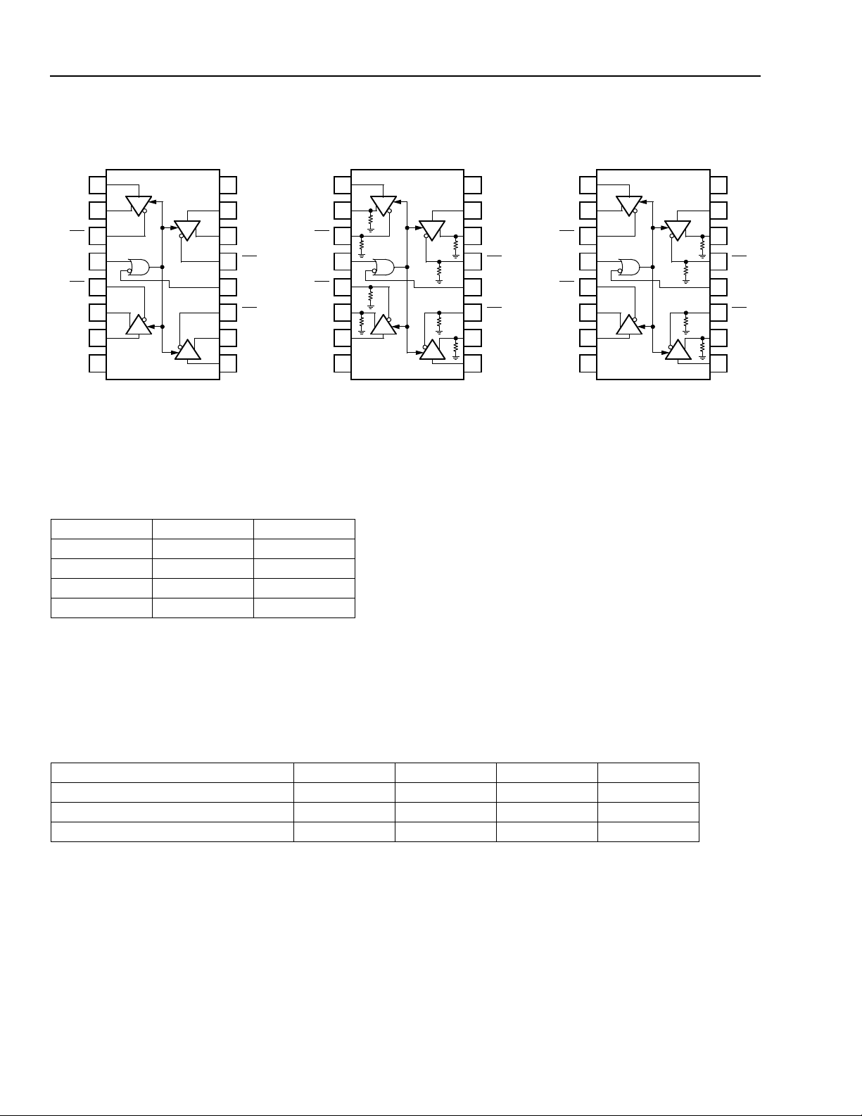
Pin Information
Data Sheet
January 1999
AI
1
AO
AO
E1
BO
BO
BI
GND
A
2
3
4
5
6
B
7
8
D
C
BDG1A
BDGLA
BPNGA
Table 1. Enable Truth Table
E1 E2 Condition
00Active
10Active
01Disabled
11Active
V
CC
16
DI
15
DO
14
DO
13
E2
12
CO
11
CO
10
CI
9
AO
AO
E1
BO
BO
GND
AI
1
A
2
3
4
5
6
BI
B
7
8
D
C
V
CC
16
DI
15
DO
14
DO
13
E2
12
CO
11
CO
10
CI
9
BDP1A
BPNPA
Figure 1. Quad Differential Driver Logic Diagrams
AO
AO
E1
BO
BO
GND
AI
1
A
2
3
4
5
6
BI
B
7
8
D
C
V
CC
16
DI
15
DO
14
DO
13
E2
12
CO
11
CO
10
CI
9
BPPGA
12-2038b (F)
Absolute Maximum Ratings
Stresses in excess of the absolute maximum ratings can cause permanent damage to the device. These are absolute stress ratings only. Functional operation of the device is not implied at these or any other conditions in excess
of those given in the operational sections of the data sheet. Exposure to absolute maximum ratings for extended
periods can adversely affect device reliability.
Parameter Symbol Min Max Unit
Power Supply Voltage V
Ambient Operating Temperature T
Storage Temperature T
2 Lucent Technologies Inc.
CC
A
stg
—6.5V
40 125 °C
−
55 150 °C
−
Data Sheet
January 199 9
BDG1A, BDP1A, BDGLA, BPNGA, BPNPA, and BPPGA
Quad Differential Drivers
Electrical Characteristics
For electrical characteristics over the entire temperature range, see Figures 7 through 9.
Table 2. Power Supply Current Characteristics
A
= –40 °C to +125 °C, V
T
CC
= 5 V ± 0.5 V.
Parameter Symbol Min Typ Max Unit
Power Supply Current (V
CC
= 5.5 V):
All Outputs Disabled:
BDG1A*, BPNGA* I
BDP1A
†
, BPNPA
†
BDGLA* I
BPPGA*
†
CC
CC
I
CC
CC
I
45 65 mA
120 160 mA
35 55 mA
85 115 mA
All Outputs Enabled:
BDG1A*, BPNGA* I
BDP1A
†
, BPNPA
†
BDGLA* I
BPPGA*
* Measured with no load (BPPGA has no load on drivers C and D).
† The additional power dissipation is the result of integrating the termination resistors into the device. I
across the driver outputs (BPPGA has terminating resistors on drivers A and B).
†
CC
CC
I
CC
CC
I
25 40 mA
150 200 mA
14 20 mA
90 115 mA
CC
is measured with a 100 Ω resistor
Third State
These drivers produce pseudo-ECL levels, and the third-state mode is different than the conventional TTL devices.
When a driver is placed in the third state, the bases of the output transistors are pulled low, bringing the outputs
below the active-low levels. This voltage is typically 2 V for most drivers. In the bidirectional bus application, the
driver of one device, which is in its third state, may be back driven by another driver on the bus whose voltage in the
low state is lower than the third-stated device. This could come about due to differences in the drivers’ independent
power supplies. In this case, the device in the third state will control the line, thus clamping the line and reducing
the signal swing. If the difference voltage between the independent power supplies and the drivers is small, then
this consideration can be ignored. In the typical case, the difference voltage can be as much as 1 V without significantly affecting the amplitude of the driving signal.
Lucent Technologies Inc. 3

Quad Differential Drivers
BDG1A, BDP1A, BDGLA, BPNGA, BPNPA, and BPPGA
Data Sheet
January 1999
Electrical Characteristics
(continued)
Table 3. Voltage and Current Characteristics
For the variation in V
A
T
= –40 °C to +125 °C.*
OH
and V
OL
over the temperature range, see Figures 7 and 8.
Parameter Symbol Min Typ Max Unit
Output Voltages:
Low* V
OL
V
OH –
1.4 V
OH
1.1 V
−
OH
0.65 V
−
High*:
BDG1A, BDP1A, BPNGA, BPNPA, BPPGA V
BDGLA V
OH
Differential Voltage (V
Output Voltages (T
A
= 0 °C to 85 °C):
– VOL)V
Low* V
OH
OH
DIFF
OL
CC
V
CC
V
1.8 V
−
2.5 V
−
CC
1V
−
CC
2V
−
CC
0.8 V
−
CC
1.6 V
−
0.65 1.1 1.4 V
V
OH –
1.4 V
OH
1.1 V
−
OH
0.8 V
−
High*:
BDG1A, BDP1A, BPNGA, BPNPA, BPPGA V
BDGLA V
OH
Differential Voltage (V
Third State, I
OH
= –1.0 mA, VCC = 4.5 V:
– VOL)V
BDG1A, BDP1A, BPNGA, BPNPA, BPPGA V
BDGLA V
OH
OH
DIFF
OZ
OZ
CC
V
CC
V
1.5 V
−
2.5 V
−
CC
1V
−
CC
2V
−
CC
0.8 V
−
CC
1.6 V
−
0.8 1.1 1.4 V
—V
OL
0.5 V
−
OL
0.2 V
−
—0.20.5V
Input Voltages:
CC
Low, V
Data Input V
Enable Input V
High, V
Clamp, V
Short-circuit Output Current, V
Input Currents, V
Low, V
High, V
Reverse, V
= 5.5 V:
†
CC
= 4.5 V V
CC
= 4.5 V, II = –5.0 mA V
CC
= 5.5 V I
CC
= 5.5 V:
I
= 0.4 V I
I
= 2.7 V I
I
= 5.5 V I
OS
IL
†
IL
IH
IK
‡
IL
IH
IH
——0.8V
——0.7V
2.0 — — V
——−1.0 V
–100 — — mA
——−400
——20 µA
— — 100
Output Resistors:
BDP1A, BPNPA, BP PGA
* Values are with terminations as per Figure 4 or equivalent.
† The input levels and diff erence voltage provide zero noise immunity and should be tested only in a static, noise-free environment.
‡ Test must be performed one lead at a time to prevent damage to the device.
§ See Figure 1 for BPPGA terminations.
§
O
R
— 220 —
µ
µ
A
A
Ω
4 Lucent Technologies Inc.
Data Sheet
January 199 9
BDG1A, BDP1A, BDGLA, BPNGA, BPNPA, and BPPGA
Timing Characteristics
Table 4. Timing Characteristics (See Figures 2 and 3.)
P1
For t
and tP2 propagation delays over the temperature range, see Figure 9.
Propagation delay test circuit connected to output (see Figure 6).
Quad Differential Drivers
A
T
= –40 °C to +125 °C, V
CC
= 5 V ± 0.5 V.
Parameter Symbol Min Typ Max Unit
Propagation Delay:
Input High to Output
Input Low to Output
Capacitive Delay
†
†
tP1* 0.8 1.2 2.0 ns
tP2* 0.8 1.2 2.0 ns
p
t
∆
— 0.02 0.03 ns/pF
Disable Time (either E1 or E2):
High-to-high Impedance t
Low-to-high Impedance t
PHZ
PLZ
4 8 12 ns
4 8 12 ns
Enable Time (either E1 or E2):
High Impedance to High t
High Impedance to Low t
Output Skew, |t
PHH – tPHL
|t
P1
– tP2|t
PLH
|, |t
PLL
– t
|t
Difference Between Drivers
Rise Time ( 20%—80%) t
Fa ll Time (80%—20%) t
*tP1 and tP2 are measured from the 1.5 V point of the input to the crossover point of the outputs (see Figure 2).
† CL = 5 pF. Capacitor is connected from each output to ground.
PZH
PZL
skew1
skew2
t
∆
skew
tLH
tHL
4 8 12 ns
4 8 12 ns
—0.10.3ns
—0.20.5ns
——0.3ns
—0.7 2 ns
—0.7 2 ns
Lucent Technologies Inc. 5
 Loading...