

AGERE ATTL7591AS, ATTL7591AB Datasheet
Data Sheet
October 1997
L7591 Subscriber Line Interface Circuit Protector
Features
■
Shunts lightning pulses to ground
— Positive or negative 30 A, 10 x 1000 µs
— Positive or negative 40 A, 5 x 320 µs
— Positive or negative 80 A, 2 x 10 µs
■
Power-cross protection
— 3.5 A
— 5.0 A
■
Gate trigger current, 15 mA max
■
Up to –80 V capability
■
Holding current, 150 mA min
PEAK
, 50 Hz to 60 Hz, 1 s
PEAK
, 50 Hz to 60 Hz, 10 ms
Pin Information
Table 1. Pin Description
(Applies to DIP and SONB packages)
Pin Symbol Name/Function
1 TIP Tip signal from customer.
2V
3 — Test Point, do not use.
4 RING Ring signal from customer.
5 PR Protected ring signal to line-feed-
6 GND Device ground/fault current
7 GND Device ground/fault current
8 PT Protected tip signal to line-feed
Note: Pins 1 and 4 must always be connected to the protection
S
Supply voltage to gate
(–20 V to –80 V).
circuitry.
return.
return.
circuitry.
resistors shown in Figures 4 and 5 (Line Feed Circuitry). The
SLIC can be connected either to the protected outputs (pins
5 and 8) or to the inputs (pins 1 and 4).
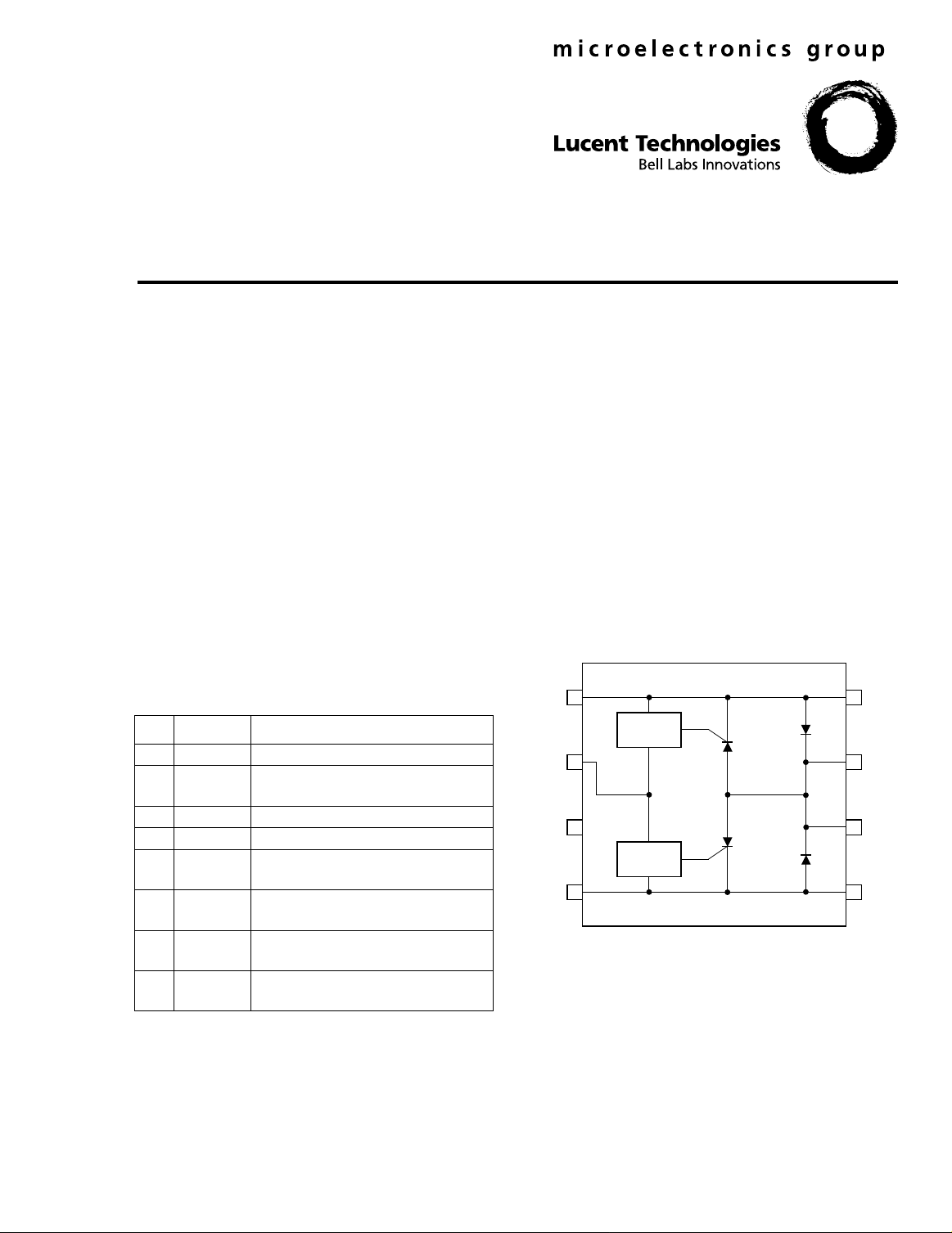
Description
The L7591 Subscriber Line Interface Circuit (SLIC)
Protector is designed to protect line-feed circuitry
from fault-induced lightning and power-cross surge
pulses. If a fault current forces TIP and/or RING to a
more negative voltage than VS, current is conducted
through the trip circuit. When the specified trip current level is reached, transistors PNPN1 and/or
PNPN2 will turn on and "crowbar" the majority of the
current to ground. If similar pulses force TIP and/or
RING to a more positive state than ground, diodes
D1 and/or D2 will conduct the pulse to ground. The
L7591 SLIC Protector is available in an 8-pin, plastic
DIP (L7591AB) and in an 8-pin, plastic SONB package (L7591AS).
PT
D1
D2
8
GND
7
6
GND
5
PR
12-1590 (C)
TIP
1
TRIP
TEST
POINT
RING
CIRCUIT
S
V
2
3
TRIP
CIRCUIT
4
PNPN1
PNPN2
Figure 1. Functional and Pin Diagram
L7591 Subscriber Line Interface Circuit Protector
Data Sheet
October 1997
Absolute Maximum Ratings
(At 25 °C)
Stresses in excess of the Absolute Maximum Ratings can cause permanent damage to the device. These are
absolute stress ratings only. Functional operation of the device is not implied at these or any other conditions in
excess of those given in the operational sections of the data sheet. Exposure to Absolute Maximum Ratings for
extended periods can adversely affect the device reliability.
Parameter Symbol Value Unit
Ambient Operating Temperature T
Storage Temperature Range T
Pin Soldering Temperature (t = 15 s max) — 300
Supply V oltage V
A
stg
–40 to +85
–40 to +125
S
–83 V
°
C
°
C
°
C
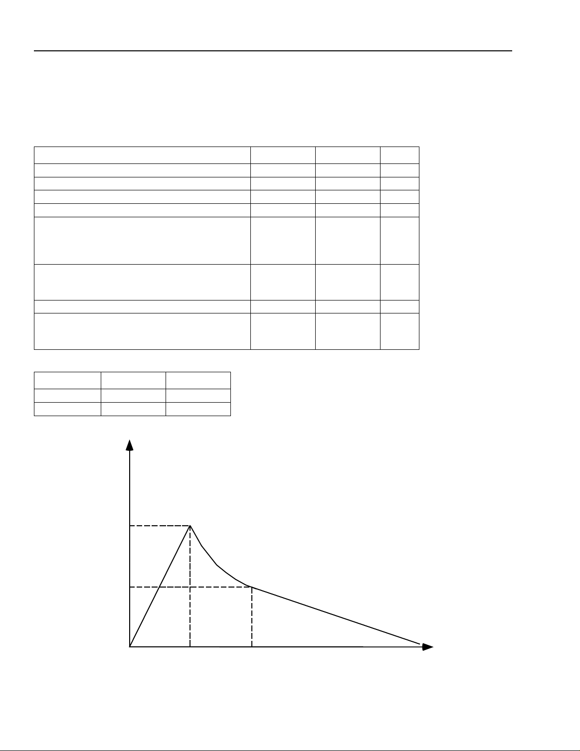
Peak Pulse Current: * (See Figure 2.)
10 x 1000 µs
5 x 320 µs
2 x 10 µs
—
—
—
30
40
80
A
A
A
Nonrepetitive Peak ON-state Current:
t = 1 s, f = 50 Hz to 60 Hz
t = 10 ms, f = 50 Hz to 60 Hz
—
—
3.5
5
A
A
Maximum Gate Current (Half Sine Wave 10 ms) — 2 A
Maximum V oltage:
TIP or RING to Gnd
VS to Gnd
—
—
–100
–80
V
V
*Pulse Wav ef orm Data:
10 x 1000 µs tr = 10 µs tp = 1000 µs
5 x 320 µs tr = 5 µs tp = 320 µs
2 x 10 µs tr = 2 µs tp = 10 µs
% IPP
100
50
0
tr tp t
Figure 2. Pulse Waveform
2 Lucent Technologies Inc.

Data Sheet
October 1997
L7591 Subscriber Line Interface Circuit Protector
Electrical Specifications
(TA = 25 °C)
The minimum and/or maximum limits specified for the parameters are based on the absolute system. The algebraic sign only applies to the direction of the parameter. These requirements apply to either the TIP or RING terminal; how e v er, the device is capab le of simultaneous Tip and Ring surges and continuous current, as noted below in
Tip and Ring leads. See Figure 3 and Table 5 for symbol and test condition definition.
Table 2. Electrical Characteristics D1 and D2
Characteristic Symbol Test Conditions Min Typ Max Unit
Forward Voltage V
Peak Forward Voltage V
FP
F
IP = 5 A, tP = 1 ms — 1.6 3 V
IPP = 30 A, 10 x 1000 µs — 5.2 15 V
Table 3. Electrical Characteristics, PNPN Circuitry
Characteristic Symbol Test Conditions Min Typ Max Unit
Gate Trigger Current I
Holding Current I
Trip V oltage V
Dynamic Trip V oltage V
GT
H
T
SGL
VS = 48 V 0.2 — 15 mA
tP = 10 ms, VS = 48 V –150 –250 — mA
dc — VS –2.0 VS –2.8 V
IPP = 30 A, VS = –48 V,
— –51 –63 V
10 x 1000 µs
Reverse Leakage Current:
I
RG
VS = –75 V
VS to Tip or Ring
TA = 25 °C
TA = 70 °C
dv/dt Sensitivity — Tip or Ring Lead
On-state V oltage: V
—
—
ON
—
—
tP = 1 ms
—
—
±
1000 — — V/µs
0.12
—
5
50
µ
A
µ
A
IT = 0.5 A — — — –1.3 — V
IT = 3.0 A — — — –2.3 — V
Table 4. Electrical Characteristics, Diode and PNPN Circuitry
Characteristic Symbol Test Conditions Min Typ Max Unit
Reverse Leakage Current:
I
R
VR = –85 V
(Gate Open)
TA = 25 °C
TA = 70 °C
Off-state Capacitance:
VR = –3 V
VR = –48 V
—
—
C
off
—
—
—
—
f = 1 MHz
—
—
—
—
—
—
0.14
—
50
40
5
50
—
—
µ
µ
pF
pF
A
A
Lucent Technologies Inc. 3
 Loading...