

AGERE ATTL7583DF, ATTL7583DAJ-D, ATTL7583CF, ATTL7583CAJ-D, ATTL7583BF Datasheet
...
Data Sheet
February 2001
L7583A/B/C/D Line Card Access Switch
Features
■ Small size/surface-mount packaging
■ Monolithic IC reliability
■ Low impulse noise
■ Make-before-break, break-before-make operation
■ Clean, bounce-free switching
■ Low, matched ON-resistance
■ Built-in current limiting, thermal shutdown, and
SLIC protection
■ 5 V only operation, very low power consumption
■ Battery monitor, all OFF state upon loss of battery
■ No EMI
■ Latched logic level inputs, no driver circuitry
■ Only one external protector required
Applications
■ Central office
■ DLC
■ PBX
■ DAML
■ HFC/FITL
The L7583A/B has seven states: the idle talk state
(line break switches closed, all other switches open),
the power ringing state (ringing access switches
closed, all other switches open), loop access state
(loop access switches closed, all switches open),
SLIC test state (test in switches closed, all other
switches open), simultaneous loop and SLIC
access state (loop and test in switches closed, all
others open), ringing generator test state (ring test
switches closed, all others open), and an all OFF
state. The seven states in the L7583A/B are also in
the L7583C/D, with an additional simultaneous testout and ring-test state, making the L7583C/D appropriate for digital loop carrier and other Bellcore TR-57
applications.
The L7583 offers break-before-make or makebefore-break switching, with simple logic level input
control. Because of the solid-state construction, voltage transients generated when switching into an
inductive ringing lead during ring cadence or ring trip
are minimized, possibly eliminating the need for
external zero cross switching circuitry. State control
is via logic level inputs, so no additional driver circuitry is required.
The line break switch is a linear switch that has
exceptionally low ON-resistance and an excellent
ON-resistance matching characteristic. The ringing
access switch has a breakdown voltage rating
>480 V which is sufficiently high, with proper protection, to prevent breakdown in the presence of a transient fault condition (i.e., passing the transient on to
the ringing generator).
Description
The L7583A/B/C/D Line Card Access Switch is a
monolithic solid-state device providing the equivalent
switching functionality of three 2 form C switches.
The L7583 is designed to provide power ringing
access, line test access (test out), and SLIC test
access (test in) to tip and ring in central office, digital
loop carrier, private branch exchange, digitally added
main line, and hybrid fiber coax/fiber-in-the-loop analog line card applications. An additional pair of solidstate contacts are also available to provide access
for testing of the ringing generator.
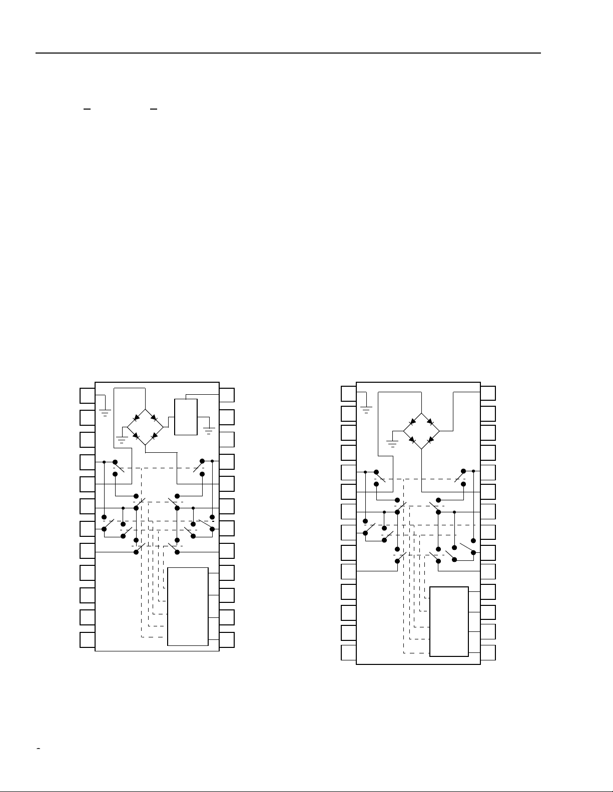
Incorporated into the L7583A
xx and L7583Cxx is a
diode bridge/SCR clamping circuit, current-limiting
circuitry, and a thermal shutdown mechanism to provide protection to the SLIC device and subsequent
circuitry during fault conditions. This is shown in Figure 1 as version A. Positive and negative lightning is
reduced by the current-limiting circuitry and steered
to ground via diodes and the integrated SCR. Power
cross is also re duced
by the current-limiting and ther-
mal shutdown circuits.
24
23
22
21
20
19
18
17
16
15
14
13
1
2
3
4
5
6
7
V
BAT
RBAT
RLINE
NC
F
GND
NC
NC
T
LINE
VDD
SW1
8
9
10
LATCH
R
RINGING
TTESTout
SW2
SW3 SW4
SW5
SW7
SW9
SW8
SW10
SW6
TTESTin
TBAT
TRINGING
NC
IN
TESTin
RTESTout
RTESTin
NC
11
12
IN
RING
DGND
TSD
INTESTout
CONTROL
LOGIC
SCR
AND
TRIP
CKT
L7583A/B/C/D Line Card Access Switch
Data Sheet
February 2001
Description (continued)
The L7583B
integrated diode bridge along with current limiting and
thermal shutdown (see Figure 2 for version B). This will
cause positive faults to be directed to ground and negative faults to battery. In either polarity, faults are
reduced by the current-limit and/or thermal shutdown
mechanisms.
To protect the L7583 from an overvoltage fault condition, use of a secondary protector is required. The secondary protector must limit the voltage seen at the tip/
ring terminals to prevent the breakdown voltage of the
switches from being exceeded. To minimize stress on
the solid-state contacts, use of a foldback- or crowbartype secondary protector is recommended. With proper
choice of secondary protection, a line card using the
L7583 will meet all relevant ITU-T, LSSGR, FCC, or
UL
* protection requirements.
xx and L7583Dxx versions provide only an
Pin Information
The L7583 operates off of a 5 V supply only. This gives
the device extremely low idle and active power dissipation and allows use with virtually any range of battery
voltage. This makes the L7583 especially appropriate
for remote power applications such as DAM L or FOC/
FITL or other Bellcore TA 909 applications where
power dissipation is particularly critical.
A battery voltage is also used by the L7583, only as a
reference for the integrated protection circuit. The
L7583 will enter an all OFF state upon loss of battery.
During power ringing, to turn on and maintain the ON
state, the ring access switch and ring test switch will
draw a nominal 2 mA or 4 mA from the ring generator.
The L7583A/B/C/D device is packaged in a 24-pin,
plastic DIP (L7583AF/BF/CF/DF) and in a 28-pin,
plastic SOG (L7583AAJ/BAJ/CAJ/DAJ).
* UL is a registered trademark of Underwriters Laboratories, Inc.
SW2
SW6
SW8
28
27
26
25
24
23
22
21
20
19
18
17
16
15
BAT
V
NC
NC
NC
RTESTin
RBAT
RLINE
NC
RINGINGNC
R
RTESTout
LATCH
INTESTin
RING
IN
INTESTout
12-2365.d (F)
12-2364.a (F)
Note: Shown with A/C version protection. The 24-pin DIP is avail-
able with either A/C or B/D version protection.
Figure 1. 24-Pin, Plastic DIP (600 mil)
1
F
GND
2
NC
3
NC
4
NC
TTESTin
TBAT
LINE
T
TRINGING
TTESTout
NC
VDD
TSD
DGND
Note: Shown with B/D version protection. The 28-pin SOG is avail-
able with either A/C or B/D version protection.
SW1
5
6
SW3 SW4
7
SW5
8
SW7
9
10
11
12
13
14
SW9
SW10
CONTROL
LOGIC
Figure 2. 28-Pin, Plastic SOG
22 Lucent Technologies Inc.
Data Sheet
February 2001
L7583A/B/C /D Line Card Access Swi t ch
Pin Information (continued)
Table 1. Pin Descriptions
DIP SOG Symbol Description DIP SOG Symbol Description
11F
2 2 NC No connection. 23 27, 26 NC No connection.
3 3, 4 NC No connection. 22 25, 21 NC No connection.
45T
56 T
67T
78T
810T
9 9, 11 NC No connection. 16 18 LATCH Data input control, active-high,
10 12 V
11 13 T
12 14 D
GND Fault ground. 24 28 VBAT Battery voltage. Used as a ref-
erence for protection circuit.
TESTin Test (in) access on TIP . 21 24 RTESTin Test (in) access on RING.
BAT Connect to TIP on SLIC side. 20 23 RBAT Connect to RING on SLIC
side.
LINE Connect to TIP on line side. 19 22 RLINE Connect to RING on line side.
RINGING Connect to return ground for ring-
18 20 RRINGING Connect to ringing generator.
ing generator.
TESTout Test (out) access on TIP. 17 19 RTESTout Test (out) access on RING.
transparent low.
DD 5 V supply. 15 17 INTEST in Logic level switch input control.
SD Temperature shutdown pin. Can
14 16 IN
RING Logic level switch input control.
be used as a logic le vel inpu t or an
output. See Tables 16 and 17,
Truth Tables, and the Switching
Behavior section of this data sheet
for input pin description. As an
output fla g, wi l l r ead 5 V w he n th e
device is in its operational mode
and 0 V in the thermal shutdown
mode. T o disable the thermal shutdown mechanism, tie this pin to
5 V (not recommended).
GND Digital ground. 13 15 INTESTout Logic level switch input control.
Absolute Maximum Ratings
Stresses in excess of the absolute maximum ratings can cause permanent damage to the device. These are absolute stress ratings only. Functional operation of the device is not implied at these or any other conditions in excess
of those given in the operational sections of the data sheet. Exposure to absolute maximum ratings for extended
periods can adversely affect device reliability.
Table 2. Absolute Maximum Ratings
Parameter Min Max Unit
Operating Temperature Range –40 110 °C
Storage Temperature Range –40 150 °C
Relative Humidity Range 5 95 %
Pin Soldering Temperature (t = 10 s max) — 260 °C
5 V Power Supply — 7 V
Battery Supply — –85 V
Logic Input Voltage — 7 V
Input-to-output Isolation — 330 V
Pole-to-pole Isola tion — 330 V
Lucent Technologies Inc. 3
L7583A/B/C/D Line Card Access Switch
Data Sheet
February 2001
Handling Precautions
Although protection circuitry has been designed into this device, proper precautions should be taken to avoid exposure to electrostatic discharge (ESD) during handling and mounting. Lucent Technologies Microelectronics Group
employs a human-body model (HBM) and a charged-device model (CDM) for ESD-susceptibility testing and protection design evaluation. ESD voltage thresholds are dependent on the circuit parameters used to define the
model. No industry-wide standard has been adopted for CDM. However, a standard HBM (resistance = 1500 Ω,
capacitance = 100 pF) is widely used and therefore can be used for comparison purposes. The HBM ESD threshold presented here was obtained by using these circuit parameters.
Table 3. HBM ESD Threshold Voltage
Device Rating
L7583 1000 V
Electrical Characteristics
TA = –40 °C to +85 °C, unless otherwise specified.
Minimum and maximum values are testing requirements. Typical values are characteristics of the device and are
the result of engineering evaluations. Typical values are for information purposes only and are not part of the testing requirements.
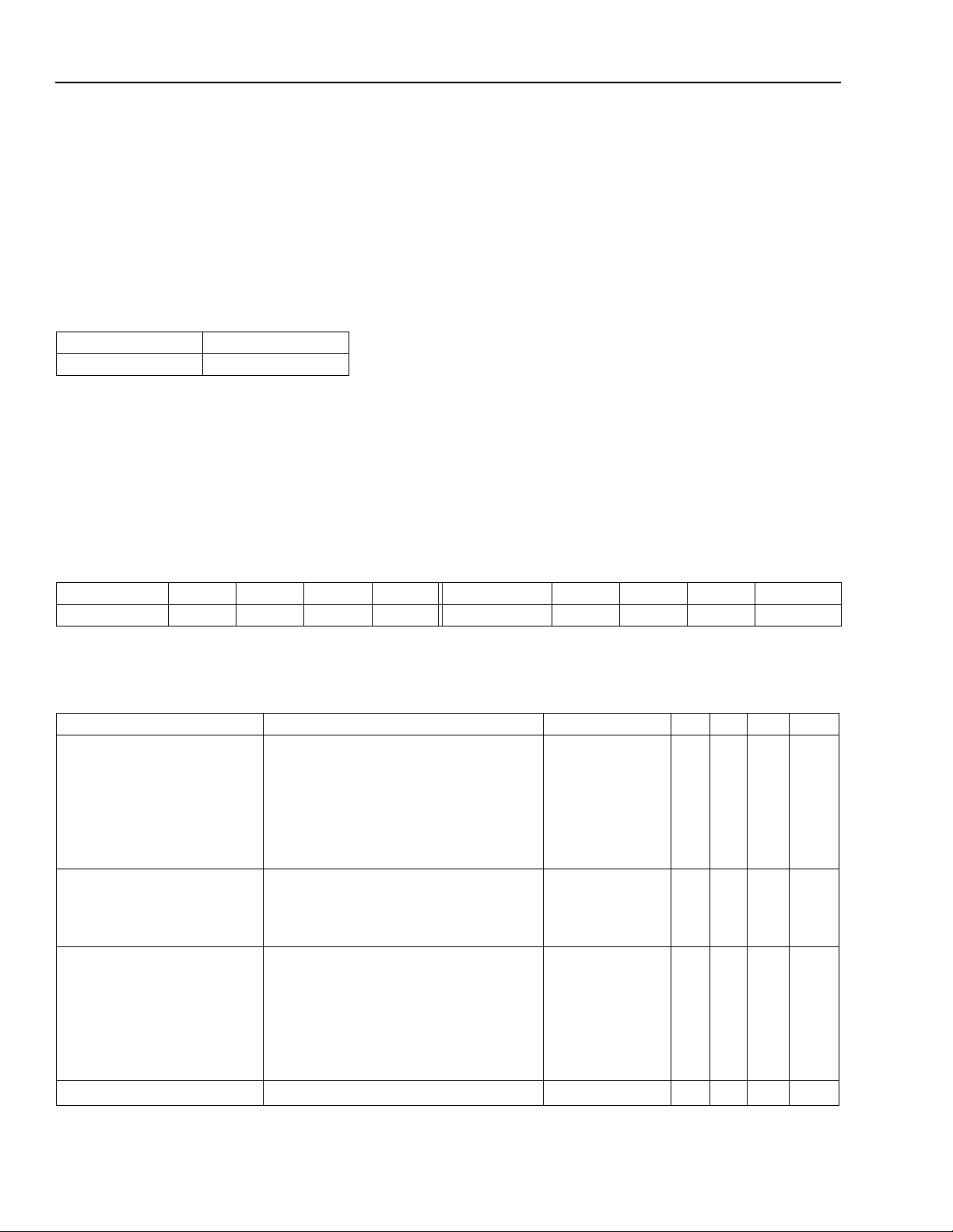
Table 4. Power Supply Specifications
Supply Min Typ Max Unit Supply Min Typ Max Unit
DD 4.5 5 5.5 V VBAT* –19 — –72 V
V
*VBAT is used only as a reference for internal protection circuitry . If VBAT rises above –10 V, the device will enter an all OFF state and remain in
this state until the battery voltage drops below –15 V.
Table 5. Test In Switches, 1 and 2
Parameter Test Condition Measure Min Typ Max Unit
OFF-state Leakage Current:
+25 °C
+85 °C
–40 °C
ON-resistance:
+25 °C
+85 °C
–40 °C
Isolation:
+25 °C
+85 °C
–40 °C
dV/dt Sensitivity*
Vswitch (differential) = –320 V to Gnd
Vswitch (differential) = –60 V to +260 V
Vswitch (differential) = –330 V to Gnd
Vswitch (differential) = –60 V to +270 V
Vswitch (differential) = –310 V to Gnd
Vswitch (differential) = –60 V to +250 V
Iswitch (on) = ±5 mA, ±10 mA
Iswitch (on) = ±5 mA, ±10 mA
Iswitch (on) = ±5 mA, ±10 mA
Vswitch (both poles) = ±320 V,
Logic inputs = Gnd
Vswitch (both poles) = ±330 V,
Logic inputs = Gnd
Vswitch (both poles) = ±310 V,
Logic inputs = Gnd
———200—V/µs
Iswitch
Iswitch
Iswitch
ON
V
∆
∆ VON
∆ VON
Iswitch
Iswitch
Iswitch
—
—
—
—
—
—
—
—
—
—
—
—
45
—
33
—
—
—
1
1
1
—
70
—
1
1
1
µA
µA
µA
Ω
Ω
Ω
µA
µA
µA
* Applied voltage is 100 Vp-p square wave at 100 Hz.
4 Lucent Technologies Inc.

Data Sheet
February 2001
Electrical Characteristics (continued)
Table 6. Break Switches, 3 and 4
Parameter Test Condition Measure Min Typ Max Unit
OFF-state Leakage
Current:
+25 °C
+85 °C
–40 °C
ON-resistance:
+25 °C
+85 °C
–40 °C
ON-resistance Match Per ON-resistance test
ON-state Voltage* Iswitch = I
dc Current Limit:
+85 °C
–40 °C
Dynamic Current Limit
(t = <0.5 µs)
Isolation:
+25 °C
+85 °C
–40 °C
dV/dt Sensitivity
†
Vswitch (differential) = –320 V to Gnd
Vswitch (differential) = –60 V to +260 V
Vswitch (differential) = –330 V to Gnd
Vswitch (differential) = –60 V to +270 V
Vswitch (differential) = –310 V to Gnd
Vswitch (differential) = –60 V to +250 V
LINE = ±10 mA, ±40 mA, TBAT = –2 V
T
LINE = ±10 mA, ±40 mA, TBAT = –2 V
T
LINE = ±10 mA, ±40 mA, TBAT = –2 V
T
condition of SW3, SW4
LIMIT @ 50 Hz/60 Hz VON — — 220 V
Vswitch (on) = ±10 V
Vswitch (on) = ±10 V
Break switches in ON state; ringing
access switches OFF; apply ±1000 V at
10/1000 µs pulse; appropriate second-
ary protection in place
Vswitch (both poles) = ±320 V,
Logic inputs = Gnd
Vswitch (both poles) = ±330 V,
Logic inputs = Gnd
Vswitch (both poles) = ±310 V,
Logic inputs = Gnd
— — — 200 — V/µs
L7583A/B/C /D Line Card Access Swi t ch
Iswitch
Iswitch
Iswitch
V
ON
∆
V
∆
ON
V
∆
ON
Magnitude
ON SW3 – RON SW4
R
Iswitch
Iswitch
Iswitch — 2.5 — A
Iswitch
Iswitch
Iswitch
—
—
1
—
—
1
—
—
1
—
—
—
19.5
14.5
—
—
28
—
—0.21.0
80————
250mAmA
—
—
1
—
—
1
—
—
1
µA
µA
µA
Ω
Ω
Ω
Ω
µA
µA
µA
* This parameter is not tested in production. Choice of secondary protector should ensure this rating is not exceeded.
† Applied voltage is 100 Vp-p square wave at 100 Hz.
Lucent Technologies Inc. 5
L7583A/B/C/D Line Card Access Switch
Electrical Characteristics (continued)
Table 7. Ring Test Return Switch, 5
Parameter Test Condition Measure Min Typ Max Unit
OFF-state Leakage Current:
+25 °C
+85 °C
–40 °C
ON-resistance Iswitch (on) = ±0 mA, ±10 mA
Isolation:
+25 °C
+85 °C
–40 °C
dV/dt Sensitivity*
Vswitch (differential) = –320 V to Gnd
Vswitch (differential) = –60 V to +260 V
Vswitch (differential) = –330 V to Gnd
Vswitch (differential) = –60 V to +270 V
Vswitch (differential) = –310 V to Gnd
Vswitch (differential) = –60 V to +250 V
Vswitch (both poles) = ±320 V,
Logic inputs = Gnd
Vswitch (both poles) = ±330 V,
Logic inputs = Gnd
Vswitch (both poles) = ±310 V,
Logic inputs = Gnd
———200—V/µs
February 2001
—
Iswitch
Iswitch
Iswitch
V
ON —50100
∆
Iswitch
Iswitch
Iswitch
—
—
—
—
—
—
—
—
—
—
—
Data Sheet
µA
1
µA
1
µA
1
Ω
µA
1
µA
1
µA
1
* Applied voltage is 100 Vp-p square wave at 100 Hz.
Table 8. Ringing Test Switch, 6
Parameter Test Condition Measure Min Typ Max Unit
OFF-state Leakage Current:
+25 °C
Vswitch (differential) = –60 V to +190 V
Iswitch
—
1
—
Vswitch (differential) = +60 V to –190 V
+85 °C
Vswitch (differential) = –60 V to +200 V
Iswitch
—
1
—
Vswitch (differential) = +60 V to –200 V
–40 °C
Vswitch (differential) = –60 V to +180 V
Iswitch
—
1
—
Vswitch (differential) = +60 V to –180 V
ON-resistance Iswitch (on) = ±70 mA, ±80 mA
V
ON ——20
∆
ON Vo ltage Iswitch (on) = ±1 mA — — — 1.5 V
Steady-state Current* — — — — 100 mA
Release Current — — — 500 — µA
Isolation:
+25 °C
Vswitch (both poles) = ±320 V,
Iswitch
—
1
—
Logic inputs = Gnd
+85 °C
Vswitch (both poles) = ±330 V,
Iswitch
—
1
—
Logic inputs = Gnd
–40 °C
Vswitch (both poles) = ±310 V,
Iswitch
—
1
—
Logic inputs = Gnd
dV/dt Sensitivity
* Choice of secondary protector and series current-limit resistor should ensure these ratings are not exceeded.
† Applied voltage is 100 Vp-p square wave at 100 Hz.
†
———200—V/µs
µA
µA
µA
Ω
µA
µA
µA
6 Lucent Technologies Inc.
 Loading...