


AGERE A1750A62RRSC10, A1750A62RRSC08, A1750A62RRSC06, A1750A62RRFC10, A1750A62RRFC08 Datasheet
...
Data Sheet, Rev. 4
June 2001
A1750A DWDM Analog
Forward-Path or Return-Path Laser Module
Features
■Low adiabatic chirp
■Excellent linearity
■Standard ITU wavelengths
■Advanced analog chip design
■Tested for forward-path or return-path applications
■Reduces equipment requirements in the hub
■Exceeds Telcordia Technologies* 468 specification.
Description
The A1750A laser module is a dense wavelengthdivision multiplexing laser with a DFB chip designed specifically for analog RF applications. The device features low adiabatic chirp to maximize signal quality in short and long lengths of fiber. The laser’s excellent inherent linearity minimizes degradation of the broadcast signals caused by the QAM channels.
Wavelength-division multiplexing (WDM) has gained widespread acceptance in the telecommunications market and is being designed into emerging cable television network architectures. Dense WDM, a method for delivering targeted QAM signals to different locations, allows multiple signal sets to be combined onto a single strand of fiber for transmission from a headend to a hub. At the hub, individual QAM signals can be selected and combined with broadcast analog channels. The A1750A DWDM laser module reduces cable network architecture fiber requirements and lessen equipment requirements in the hub.
The A1750A is available at a variety of standard ITU wavelengths. The lasers are offered as either for- ward-path (40 MHz–860 MHz) or return-path modules (5 MHz–210 MHz).
Applications
■Networks with limited fiber
■Architectures using separate optical wavelengths to carry targeted services
*Telcordia Technologies is a trademark of Telcordia Technologies Inc.
A1750A DWDM Analog |
Data Sheet, Rev. 4 |
Forward-Path or Return-Path Laser Module |
June 2001 |
|
|
Absolute Maximum Ratings
Stresses in excess of the absolute maximum ratings can cause permanent damage to the device. These are absolute stress ratings only. Functional operation of the device is not implied at these or any other conditions in excess of those given in the operational sections of the data sheet. Exposure to absolute maximum ratings for extended periods can adversely affect device reliability.
Parameter* |
Symbol |
Min |
Max |
Unit |
|
|
|
|
|
Operating Case Temperature Range |
TC |
–25 |
65 |
°C |
|
|
|
|
|
Storage Temperature Range |
Tstg |
–40 |
70 |
°C |
|
|
|
|
|
Monitor Photodiode Reverse Voltage |
VMPD |
— |
10 |
V |
|
|
|
|
|
Laser Forward Current |
IF |
— |
150 |
mA |
|
|
|
|
|
Reverse Voltage (Laser) |
VR |
— |
2 |
V |
|
|
|
|
|
TEC Current |
ITEC |
–1.5 |
1.5 |
A |
|
|
|
|
|
RF Input Power |
PRFIN |
— |
62 |
dBm V |
|
|
|
|
|
* The device can withstand continuous exposure to the specified limits without damage.
Characteristics
Table 1. Key Characteristics
Parameter |
Symbol |
Conditions |
Min |
Typ |
Max |
Unit |
|
|
|
|
|
|
|
Frequency Range:1 |
F |
— |
|
|
|
|
Return Path |
|
|
5 |
— |
210 |
MHz |
Forward Path |
|
|
40 |
— |
860 |
MHz |
|
|
|
|
|
|
|
Frequency Response:1 |
|S21| |
IF = 60 mA, |
|
|
|
|
5 MHz—210 MHz |
|
TOP = 25 °C, |
— |
±0.5 |
— |
dB |
40 MHz—860 MHz |
|
|
— |
±0.5 |
— |
dB |
|
|
|
|
|
|
|
RF Return Loss:1 |
|S21| |
IF = 60 mA, |
— |
|
|
|
5 MHz—210 MHz |
|
|
|
>16 |
— |
dB |
40 MHz—860 MHz |
|
|
|
>16 |
— |
dB |
|
|
|
|
|
|
|
Optical Output Power |
PO |
IF = IOP |
6, 8, or |
— |
— |
mW |
|
|
|
10 |
|
|
|
|
|
|
|
|
|
|
Laser Relative Intensity |
RIN |
IF = ITH + 70 mA, |
— |
< –155 |
— |
dB/Hz |
Noise |
|
T = 25 °C |
|
|
|
|
|
|
|
|
|
|
|
Composite Second Order 2, 3 |
CSO |
IF = IOP, OMI = 10% |
— |
< –50 |
— |
dBc |
Composite Triple Beat 2, 4 |
CTB |
IF = IOP, OMI = 10% |
— |
< –60 |
— |
dBc |
Available Wavelengths5 |
λ |
IP = IOP, T = TOP |
1528 |
— |
1563 |
nm |
Wavelength Drift6 |
ΔλOP |
IF = 60 mA, |
— |
— |
0.04 |
nm |
|
|
T = TOP, |
|
|
|
|
|
|
TC varied from min—>max |
|
|
|
|
|
|
|
|
|
|
|
Adiabatic Chirp |
FM |
IF = 60 mA, |
40 |
— |
100 |
MHz/mA |
|
|
TOP = 25 °C, |
|
|
|
|
|
|
measured at 500 MHz |
|
|
|
|
|
|
|
|
|
|
|
Operating Case Tempera- |
TC |
IF = IOP |
–20 |
— |
65 |
°C |
ture Range |
|
|
|
|
|
|
|
|
|
|
|
|
|
1.Tested in a 50 Ω system with 27 Ω series matching resistor.
2.Eight-channel loading, 10% OMI, 40 km fiber.
3.Measured at 42 MHz.
4.Measured at 553.25 MHz, 577.25 MHz. and 595.25 MHz.
5.Consult an Agere Systems account manager for other wavelengths.
6.Change in wavelength as case temperature is changed.
2 |
Agere Systems Inc. |
Data Sheet, Rev. 4 |
A1750A DWDM Analog |
June 2001 |
Forward-Path or Return-Path Laser Module |
|
|
Characteristics (continued)
Table 2. Additional Characteristics
Parameter |
Symbol |
Conditions |
Min |
Max |
Unit |
|
|
|
|
|
|
Bias Current1 (Operating Current) |
IB |
BOL |
— |
120 |
mA |
Threshold Current |
ITH |
25 °C, BOL |
— |
30 |
mA |
|
|
|
|
|
|
Slope Efficiency2 |
η |
IP = ITH + 20 and |
0.10 |
— |
mW/mA |
|
|
ITH + 60 |
|
|
|
|
|
|
|
|
|
Monitor Photocurrent |
IMON |
IOP = 0 mA, VRM = 5 V, |
10 |
200 |
μA/mW |
|
|
TOP = 25 °C |
|
|
|
|
|
|
|
|
|
Operating Chip Temperature3 |
TOP |
IF = IOP |
15 |
35 |
°C |
TEC Current |
ITEC |
–20 °C < TC < 65 °C, |
–1.5 |
1.5 |
A |
|
|
TOP = 15 °C—35 °C, |
|
|
|
|
|
IF = 60 mA |
|
|
|
|
|
|
|
|
|
TEC Voltage |
VTEC |
TOP = 15 °C—35 °C over T C |
–2 |
2 |
V |
|
|
|
|
|
|
Thermistor Resistance |
RTH |
TOP = 25 °C |
9.5 |
10.5 |
k Ω |
|
|
|
|
|
|
Optical Return Loss |
ORL |
TC |
40 |
— |
dB |
|
|
|
|
|
|
Side Mode Suppression Ratio |
SMSR |
IF = IOP |
30 |
— |
dB |
|
|
|
|
|
|
1.Bias point at which all specifications apply.
2.For 10 mW output power. Minimum slope efficiency is lower for lower power lasers.
3.Chip temperature at which wavelength specification is met. Operating chip temperature is reported for each laser.
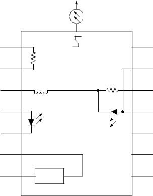
Electrical Schematics
|
1 |
|
NC |
14 |
|
|
|
|
|
|
|
|
|
|
ISOLATOR |
|
|
|
2 |
|
|
13 |
(+) |
|
3 |
|
|
12 |
(–) |
(–) |
4 |
|
|
11 |
(+) |
(+) |
5 |
|
NC |
10 |
|
|
|
|
|
|
|
(+) |
6 |
|
CASE |
9 |
|
|
|
|
|
|
|
|
|
|
GROUND |
|
|
(–) |
7 |
TEC |
CASE |
8 |
|
|
|
|
|
||
|
|
GROUND |
|
|
|
|
|
|
|
|
|
|
|
|
|
|
1-1233F |
Figure 1. A1750A Laser Schematic
Agere Systems Inc. |
3 |
 Loading...