

Page 1
SERVICE SERVICE
MANUALMANUAL
Page 2

CONTENTS
X-RAY RADIATION PRECAUTION………………………………………………………1
SAFETY PRECAUTION
…………………………………………………………………..
1
PRODUCT SAFETY NOTICE…………………………………………………………….2
GENERAL INSTRUCTION……………………………………………………………………2
ALIGNMENT ITEMS AND PROCEDURE………………………………………………..2
FACTORY ADJUSTMENT MODE
…………………………………………………………
4
ADJUSTMENT METHOD………………………………………………………………………4
CHECKING POINTS……………………………………………………………………………6
OUT-FACTORY MODE PRESET……………………………………………………………7
POWER ADAPTABILITY CHECK
……………………………………………………………
USA CHANNEL FREQUENCY TABLE (181 CH)
………………………………………
7
16
WIRING DIAGRAM……………………………………………………………………….18
BLOCK DIAGRAM………………………………………………………………………...19
IC BLOCK DIAGRAM……………………………………………………………………..20
SCHEMATIC DIAGRAM
………………………………………………………………….
28
ELECTRICAL PARTS LIST………………………………………………………………30
1
Page 3

CAUTION: THIS SERVICE MANUAL IS ONLY FOR PROFESSIONAL SERVICE PERSONNEL’S
REFERENCE. BEFORE SERVICING THIS CHASSIS, PLEASE READ THE FOLLOWING
NOTICE ITEMS.
1. SAFETY INSTRUCTION AND GENERAL INSTRUCTION
Before servicing and aligning this equipment, please read the following “X-RAY RADIATION
PRECAUTION” ,“SAFETY PRECAUTION” and “PRODUCT SAFETY NOTICE”.
1.1 X-RAY RADIATION PRECAUTION
1. Excessive high voltage can produce potentially hazardous X-RAY RADIATION. To avoid such hazards,
the high voltage must not be above the specified limit. The normal value of the high voltage of this receiver is
under 32 kV at zero beam current (minimum brightness) under DC135V main power(B+) , the high voltage
must not, under any circumstances, exceed 35 kV.
2. Each time a receiver requires servicing, the high voltage should be checked following the HIGH
VOLTAGE CHECK procedure in this manual. It is recommended the reading of the high voltage be recorded as
a part of service record. It is important to use an accurate and reliable high voltage meter.
* When checking, main power (B+) should be kept at 135 V.
3. The primary source of X-RAY RADIATION in this TV receiver is the picture tube. For continuous X-RAY
RADIATION protection, the replacement tube must be exactly the same type tube as specified in the parts list.
4. Some parts in this receiver have special safety-related characteristics for X-RAY RADIATION protection.
For continuous safety, parts replacement should be undertaken only after referring to the PRODUCT SAFETY
NOTICE below.
1.2 SAFETY PRECAUTION
WA RN I N G:
Service should not be attempted by anyone unfamiliar with the necessary precaution on this receiver. The
following are the necessary precautions to be observed before servicing this chassis.
1) Since the power supply circuit of this receiver is directly connected to the AC power line, an isolation
transformer should be used during any dynamic service to avoid possible shock hazard.
2) Always discharge the picture tube anode to the CRT conductive coating before handling the picture tube.
The picture tube is highly evacuated and if broken, glass fragments will be violently expelled. Use shatter
proof goggles and keep picture tube away from the unprotected body while handling.
3) When replacing a chassis in the cabinet, always be certain that all the protective devices are put back in
place, such as: non-metallic control knobs, insulating covers, shields, isolation resistor-capacitor network
etc.
4) When replacing parts or circuit boards, disconnect the power cord.
5) When replacing a high wattage resistor (oxiode metal film resistor) on the circuit board, keep the resistor
10mm (1/2in) away from circuit board.
6) Connection wires must be kept away from components with high voltage or high temperature.
1
Page 4

7) If any fuse in this TV receiver is blown, replace it with the FUSE specified in the chassis parts list.
1.3 PRODUCT SAFETY NOTICE
Many electrical and mechanical parts in the chassis have special safety-related characteristics. These
characteristics are often passed unnoticed by a visual inspection and the X-RAY RADIATION protection
afforded by them cannot necessarily be obtained by using replacement components rated for higher
wattage, etc. Replacement parts which have these special safety characteristics are identified in this manual
and its supplement electrical components having such features are shaded on the schematic diagram and
the parts list.
Before replacing any of these components, read the parts list in this manual carefully. The use of substitute
replacement parts which do not have the same characteristics as specified in the parts list may create shock,
fire, X-RAY RADIATION or other hazards.
1.4 General instruction
1.4.1 This chassis’ EEPROM(N801 M24C08) should copy standard data first, if necessary, deal it with
2
“factory adjustment”. If directly use blank EEPROM, should first preset I
C data, then go on other
common alignment. For factory adjustment method, refer to The appendix: Factory adjustment
mode.
If without special indication, the alignment is conducted on the below condition:
1.4.2
a)
AC power supply 120 V/60 Hz.
The whole unit is preheated for more than 30 min.
b)
(North America area) or others (depending on selling market).
1.4.3
There is built-in auto degaussing circuit, it will degauss automatically within 1second after turning on.
And the auto degaussing circuit can effect only when turning off the set and waiting for at least 30min
and then turning on.
1.4.4
If CRT is with magnetism and affects color purity and convergence, the internal degaussing can not
degauss completely, can use degaussor to degauss externally. If color purity and convergence is still poor,
then do color purity and convergence adjustment.
2 Alignment items and procedure
2.1 B+ voltage check
2.2 OSD character center adjustment
2.3 RFAGC voltage adjustment
2.4 Focus adjustment
2.5 Screen-grid voltage and white balance adjustment
2.6 SECAM colour adjustment
2.7 Horizontal, vertical scanning center adjustment
2.8 Horizontal, vertical scanning amplitude adjustment
2.9 Raster correction adjustment
2.10 The alignment flow chart see below figure.
2
Page 5
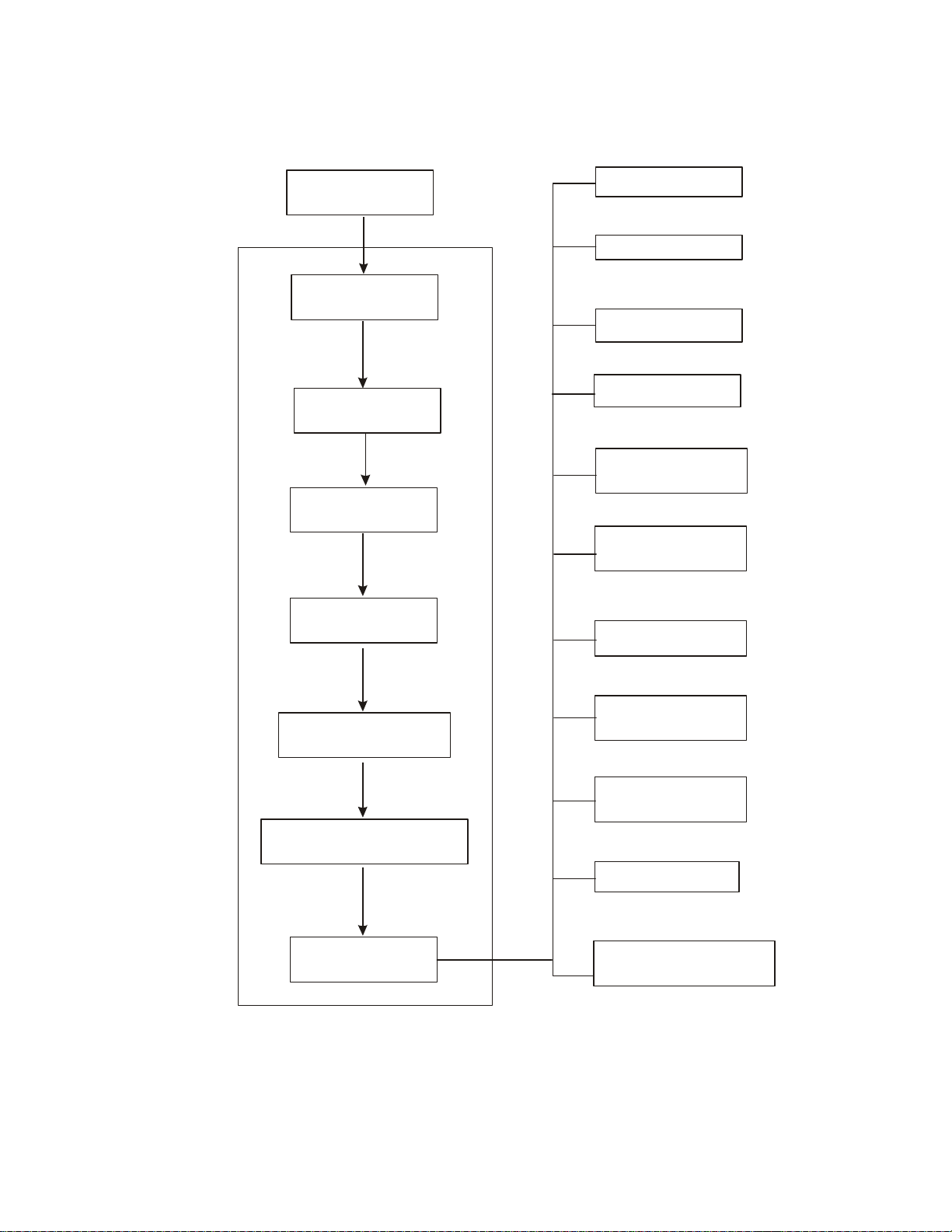
EEPROM copy
High voltage check
X-ray protection check
B+ check
Filament voltage check
OSD position
SELF CHECK
RFAGC adjustment
Picture and sound
Stereo/mono/SAP
Sub-brightness check
FOCUS
White balance check
Screen-grid voltage
White balance adjustment
Color purity
convergence check
¡¢
Scanning amplitude center &
raster correction adjustment
AV terminals
Video/S-VHS/DVD
Self alignment
Check
The TV set & remote
controller's function check
Figure 1: Alignment flow chart
3
Page 6

3 Factory adjustment mode
3.1 Enter into factory adjustment menu
Press SLEEP→PIC→DSP→MENU button on the remote controller in order (the period of two press
should be less than 5 seconds), the screen will appear factory alignment menu.
3.2 Factory menu operation
Repeatedly press“MENU” button, then the menu will enter into PAGE 1→PAGE 2→PAGE 3→
PAGE 4→PAGE 5 and recycle: press ▲ or ▼ button can select adjustment items upward or
downward, and press ◄ or ► button to confirm or adjust the item’s value.
3.3 To exit the factory menu
Press “SLEEP”button to exit the factory adjustment menu.
4 Adjustment method
4.1 B+ voltage adjustment
a) Make sure the power supply is AC120 V/60 Hz(for America or Canada area).
b) Connect the digital voltmeter to B+ testing point, receive A7 signal, set the picture control to
“NATURAL”status, adjust RP501 to make B+ voltage be 135 V±0.3 V.
c) In STAND BY mode, the B+ voltage will be about 84 V.
4.2 OSD position adjustment
Receive NTSC signal, change the factory adjustment menu page 3 OSD item’s value to make user’s
menu be in screen’s center position.
4.3 AGC adjustment
a) Receive 60 dB split field (or grey-scale) signal.
b) Use oscilloscope or digital voltmeter to monitor tuner 1 pin’s voltage (RFAGC pin).
c) Select factory adjustment menu page 4 R-AGC item, making use of [←][ →] button to increase the
value from down to up until the voltage just reach 4.0 V, at this time picture noisy spots should
disappear basically. Otherwise continue to fine tune R-AGC item.
d) Exit the factory menu.
4.4 Focus adjustment
4.4.1 Receive A12 signal, set picture mode to “MEMORY 2”status.
4.4.2 Adjust FBT FOCUS potentiometer to make screen’s B area’s focus optimum.
4.5 Screen-grid voltage,white balance adjustment
4.5.1 Receive A7 split field signal, set picture mode to “MEMORY 3” status.
4.5.2 Keep RCUT’s value, not change it (for example set it to 60), roughly adjust GCUT and BCUT
value to make white balance basically normal.
4.5.3 Set colour,contrast to minimum, set brightness to 50. Use oscilloscope to monitor CRT board red
gun waveform, adjust PAGE 4 BRTS value to make black level be 180 V.
4.5.4 Adjust SCREEN(accelerating electrode) potentiometer to make picture brighten 4 lattices.
4.5.5 Fine adjust white balance (colour temperature) 12000K±8MPCD X=0.270±0.008 Y=0.283±
4
Page 7

0.008).
4.5.6 Adjust PAGE 2 BRTN value to make colour ,brightness,contrast all be minimum, picture“white
block”slightly lights up.
4.6 Horizontal,vertical scanning center adjustment
4.6.1 PAL(50 Hz)horizontal,vertical center adjustment
Receive G23 signal, set picture mode to “ MEMORY 2 ” status, fine tune vertical center
VP50,horizontal center HPOS, to make picture center be in accordance with screen center.
4.6.2 NTSC(60 Hz)H-center,V-center adjustment
Receive A6 signal, set picture mode to “MEMORY 2” status, adjust V-center VP60, H-center HPS,
to make picture center be in accordance with screen center.
4.7 Vertical scanning amplitude adjustment
4.7.1 PAL(50 Hz)vertical amplitude adjustment
Receive D35 signal, set picture mode to “MEMORY 2” status, adjust vertical amplitude HIT, to
make picture up/down overscanning be screen size’s 8%.
4.7.2 NTSC(60 Hz)vertical amplitude adjustment
Receive A12 signal, set picture mode to “MEMORY 2”status, adjust V-amplitude HITS, to make
picture up/down overscanning be screen size’s 8%.
4.8 Raster correction adjustment,H-amplitude adjustment
4.8.1 PAL(50 Hz)raster correction adjustment ,H-amplitude adjustment.
Receive PAL white crosshatch signal, set picture mode to “MEMORY 2” status, adjust DPC to
make raster distortion be in minimum, adjust WID to make picture left/right overscanning be
screen size’s 8%.
4.8.2 NTSC(60 Hz)raster correction adjustment
Receive NTSC A21 signal, set picture mode to “MEMORY 2” status, adjust DPCS to make raster
distortion minimum, adjust WIDS to make picture left/right overscanning be screen size’s 8%.
4.9 If scanning linearity distortion and raster geometrical distortion can not reach the requirements, and
if necessary, can make use of factory adjustment menu to adjust the following items:
VLIN V-linearity adjustment(PAL)
VLIS V-linearity adjustment (NTSC)
VSC Vertical S-correction adjustment (PAL)
VSS Vertical S-correction adjustment (NTSC)
CNRT Top corners’ correction
CNRB Bottom corners’ correction
KEY Trapezoid correction (PAL)
KEYS Trapezoid correction(NTSC)
4.10 Maximum sound output power
Receive single tone signal, set volume to maximumthe sound output power is 2×8 W. (can fine adjust
factory menu V100)
5
Page 8

5 Checking points
5.1 High voltage check
5.1.1 Connect high voltmeter to CRT second anode and GND.
5.1.2 Receive A7 signal, set picture mode to “MEMORY 2” status, measure the high voltage value, the
reading should be 30.0 kV±1 kV.
5.1.3 When setting brightness and contrast to minimumzero beam currentmeasure the high voltage
value, the reading should not exceed 32 kV.
5.2 CRT filament voltage check
Receive A7 signal, set picture mode to “NATURAL” status, use effective value voltmeter to measure
CRT filament voltage, the reading should be (6.3±0.3)Vrms.
5.3 X-ray protection check
5.3.1 Receive A7 signal, set picture mode to “MEMORY 2” status.
5.3.2 Short S301, X-ray protection circuit should effect.
5.4 “Self-check”function check
Press “SELF-CHECK”button, the screen will display the following information:
M
SELF CHECK
BUS LINE:
OK
BUS CONT: OK
SYNC: OK
“OK” means bus, SYNC status, etc are normal.
If display “SCL-GND”, means SCL short to GND. ;
“SDA-GND”means SDA short to GND.
“SCL-SDA” means SCL short to SDA.
5.5 Picture and sound check
5.5.1 Receive standard TV signal.
5.5.2 Make use of picture control buttons to check colour,contrast,brightness,sharpenss,tint’s control
function.
5.5.3 Make use of sound control buttons to check sound control function.
5.6 Sub-brightness check.
Receive A7 signal, set colour,contrast,brightness all to 0, picture left one lattice slightly lights up.
5.7 This set can produce 14 kinds of testing signals by itself. In factory menu when select some
adjustment item, every press of AV button for one time, it will produce one testing signal.
5.8 Colour purity and convergence check(in normal way)
5.9 AV terminal input/output check
6
Page 9

5.10 Other control buttons on the set/remote controller function check
e
t
n
h
l
r
t
6 Out-factory mode preset
Press“SHOP OUT” button, out-factory status will be preset to:
6.1 Picture menu: Colour 70
Brightness 70
Contrast 100
Sharpness 50
Tint 50
Blue background On
6.2 Volume preset to: 30
6.3 Language menu: ENGLISH
6.4 Colour system : AUTO
6.5 NOISE REDUCE: OFF
6.6 TV mode: Channel positionA2
6.7 SVM: MILD
6.8 V-CHIP PASSWORD: 0000
6.9 CHILD LOCK MENU
PAS SW OR D:
0000
6.10 SOUND MODE: MEMORY 1
6.11 TV/CATV CHANNEL: Both set to ADD
6.12 CCD CHANNEL: Set to C1
6.13 V-OHIP: Set all ratings and contents to IGNORE
6.14 V-CHIP BLOCK ON/OFF: Set to ON
7 Power adaptability check
AC 120 V/60 Hz (for North America area. If have other special AC power supply requirements, then
check with requirements).
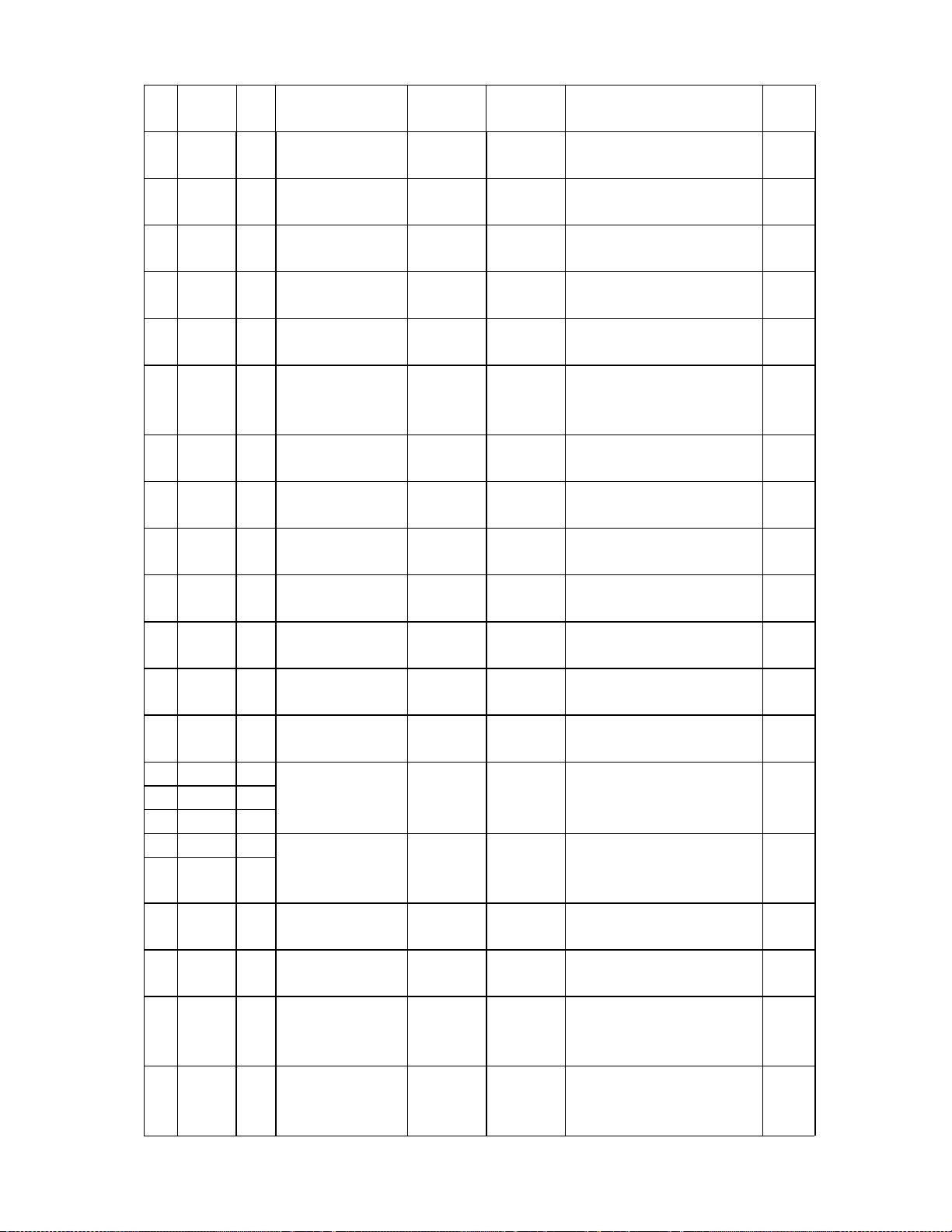
Appendix1 factory adjustment menu
Item
OSD
NO.
character
1 HPOS OF 50Hz H-center MEMORY 2 D35
2 WID 16 50Hz H-amplitude MEMORY 2 D35
3 VP50 06 50Hz V-center MEMORY 2 D35
4 VLIN 0E 50Hz V-linearity MEMORY 2 D35
5 VSC 07
6 HIT 2B 50Hz V-amplitude MEMORY 2 D35
7
Preset Adjustment item
50Hz vertica
S-correction
Analogue
setting
MEMORY 2 D35
Input
signal
Adjustment method
To make picture horizontal center b
in accordance with CRT center
To make horizontal amplitude mee
standard
To make picture vertical center be i
accordance with CRT center
To make upper,lower crosshatc
height be equal.
To make upper,middle,lowe
crosshatch height be equal.
To make Vertical amplitude mee
standard
Te st in g
point
Screen
Screen
Screen
Screen
Screen
Screen
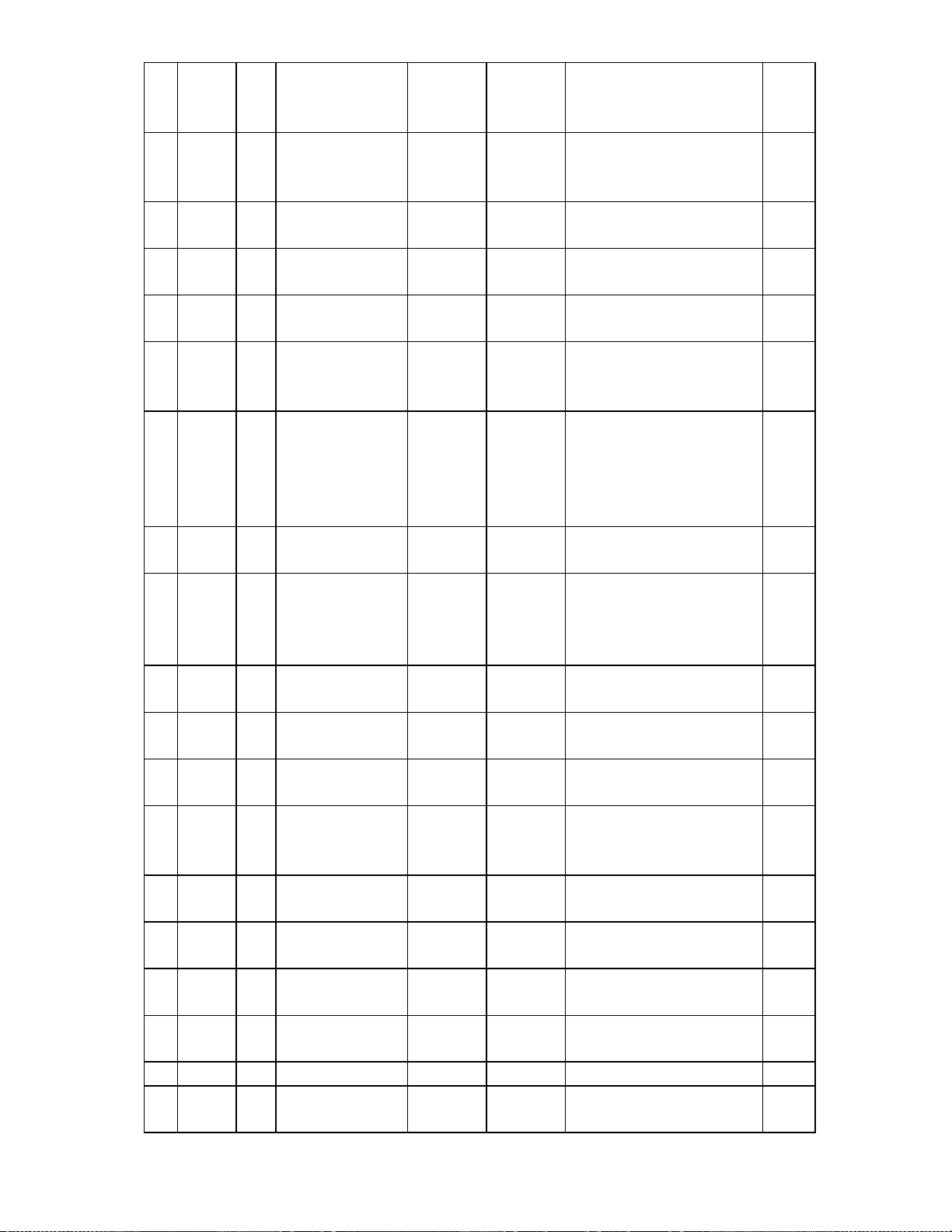
Page 10
d
n
r
r
e
e
t
n
h
l
r
t
d
n
r
r
e
e
n
e
n
m
e
m
m
7 KEY 22
8 DPC 18
9 CNRT 08
10 VEHT 05
11 HPS 04 60Hz H-center MEMORY 2 A12
12 WIDS FD 60Hz H-amplitude MEMORY 2 A12
13 VP60 02 60Hz V-center MEMORY 2 A12
14 VLIS FF 60Hz V-linearity MEMORY 2 A12
15 VSS FE
16 HITS FD 60Hz V-amplitude MEMORY 2 A12
17 KEYS 01
18 DPCS FF
19 CNRB 07
20 HEHT 02
21 RCUT 60
22 GCUT 60
23 BCUT 60
24 GDRV 30
25 BDRV 30
26 CNTX 4E
27 CNTC 30
28 CNTN 18
29 BRTX 70
50Hz trapezoi
correction
50Hz pincushio
correction
Top edge and corne
correction
Vertical high voltag
compensation
60Hz vertica
S-correction
60Hz trapezoi
correction
60Hz pincushio
correction
Bottom edge and corne
correction
Horizontal high voltag
compensation
Dark area white balanc
Bright area whit
balance
Contrast maximu
value setting
Contrast middle valu
setting
Contrast minimu
value setting
Brightness maximu
value setting
MEMORY 2 D35 To correct picture trapezoid
MEMORY 2 D35 To correct picture E/W pincushion
MEMORY 2 D35/A12
MEMORY 2 D35/A12 fix
MEMORY 2 A12
MEMORY 2 A12 To correct picture trapezoid
MEMORY 2 A12 To correct picture E/W pincushion
MEMORY 2 D35/A12
MEMORY 2 D35/A12 Fix
Black/white
MEMORY 1
MEMORY 1 Gray scale Fix
Contrast 50 Gray scale Fix
Contrast 0
Colour 0
Brightness 50
Contrast 50
Brightness 100
Colour 0
signal or A7
signal
Black/white
signal or A7
signal
Gray scale Fix
A7 signal Fix
To correct top edge and corne
vertical line
To make picture horizontal center b
in accordance with CRT center.
To make horizontal amplitude mee
standard.
To make picture vertical center be i
accordance with CRT center.
To make upper,lower crosshatc
height be equal
To make upper,middle,lowe
crosshatch height be equal.
To make vertical amplitude mee
standard
To correct bottom edge and corne
vertical line
To make picture dark area to obtai
standard “white colour”
To make picture bright area to obtai
standard “white colour”
Screen
Screen
Screen
Screen
Screen
Screen
Screen
Screen
Screen
Screen
Screen
Screen
Screen
Screen
Screen
Screen
Screen
Screen
Screen
Screen
8
Page 11
e
Contrast 0
m
e
e
e
e
Brightness 50
A7 signal Fix
Colour 0
Contrast 0
Brightness 0
A7 signal Refer to adjustment method
Colour 0
MEMORY 1 A7 signal Fix
MEMORY 2 A7 signal Fix
MEMORY 2 AVPA L Fix
Contrast 100
Brightness 50
A7 signal To make picture without colour
Colour 0
Screen
Screen
Screen
Screen
Screen
Screen
30 BRTC 50
31 BRTN 2C
32 COLX 4F
33 COLC 38
34 COLP 38
35 COLN 00
Brightness middle valu
setting
Brightness minimu
value setting
Colour maximum valu
setting
Colour middle valu
setting (NTSC)
Colour middle valu
setting (PAL)
Colour minimum valu
setting
Contrast
100
Tint 100
brightness70
A7 signal Fix Screen
36 TNTX 6F
NTSC tint maximum
value setting
colour 70
37 TNTC 38
38 TNTN 00
39 SCOL 04
40 SCNT OF
41 ASSH 00
NTSC tint middle
value setting
NTSC tint minimum
value setting
Sub-colour
adjustment
Sub-contrast
adjustment
Non-symmetry
sharpness
MEMORY 2
Contrast 100
Tint 0
brightness70
colour 70
MEMORY 2
MEMORY 2
A7 signal Fix Screen
A7 signal Fix Screen
A7 signal Fix Screen
Gray scale Fix Screen
Fix Screen
ABL control (refer to
42 ABL 27
appendix 2 for
MEMORY 1
A7 signal Fix Screen
details)
43 DEF 01
44 FLG 0 52
45 FLG 1 05
46 STBY 00
Set interlace scan to
01
Refer to appendix 2
for details
Refer to appendix 2
for details
Refer to appendix 2
for details
MEMORY 2
A7signal Fix Screen
Fix Screen
Fix Screen
Fix Screen
47 TNCD 40 Tint center(DVD) Fix Screen
48 VBLK 00
Refer to appendix 2
for details
Fix Screen
9
Page 12
49 MOD 03
50 UCOM 80
51
MODE
3
80
52 OPT 17
Refer to appendix 2
for details
Refer to appendix 2
for details
Refer to appendix 2
for details
Refer to appendix 2
for details
Fix Screen
Fix Screen
Fix Screen
Fix Screen
A2 MTS/no GAME
53
OPTM 1
(Refer to
appendix
2 for
details)
A6 MTS/ GAME
22 No MTS/no GAME
26 No MTS/ GAME
A0 MTS/no GAME/AV3
Fix Screen
A4 MTS/GAME/AV3
54
OPTM 2
(Refer to
appendix
2 for
details)
Rotation/P4.43/N4.43
C5
/M-N
Rotation/N-M/P-M/P
85
-N
No rotation
45
/N-M/P-4.43/ N-4.43
No rotation
05
/N-M/P-M/P-N
RF:N▲AV:
P/N
South
America
tri-system
RF:N;AN:P
/N
South
America
system
Fix Screen
55 TUNR 02 Tuner select Fix
Any TV
signal
display
MENU
Character in screen center Screen
56 OSD 18
OSD horizontal
position setting
content
57 OSDF 55
CCD
58
59
OSD
CCD
OSDF
16
50
60 ST3 20
61 SV3 30
OSD oscillation
frequency
CCD horizontal
position setting
CCD OSD oscillation
frequency
NTSC3.58 TV input’s
sub-sharpness middle
value
NTSC3.58 AV input’s
sub-sharpness middle
value
Fix
Display
CCD
CCD character be in screen center Screen
caption
Fix
MEMORY
2
MEMORY
2
A12 Fix Screen
AV-N3.58 Fix Screen
10
Page 13
62 SV4 30
Non NTSC3.58 AV
input’s sub-sharpness
middle value
MEMORY 2
AV-P4.43
N4.43
Fix Screen
DVD input’s
63 SVD 30
sub-sharpness middle
MEMORY 2
DVD Fix Screen
value
64 SHPX 1A
65 SHPN 1D
66 TXCX 1F
67 RGCN 1F
69 CLTM 0F
70 CLVO 4F
71 CLVD 58
Sharpness maximum
value setting
Sharpness minimum
value setting
DVD sub-colour
maximum value
DVD sub-colour
minimum value
Refer to appendix 2
for details
Refer to appendix 2
for details
Refer to appendix 2
for details
72 BRTS 20 Sub-brightness
73 RAGC 30 RF AGC
Sharpness
100
A12 Fix Screen
Sharpness 0 A12 Fix Screen
MEMORY 1
MEMORY 2
MEMORY 2
MEMORY 2
MEMORY 2
Contrast 0
Brightness 50
Colour 0
MEMORY 2
DVD Fix Screen
DVD Fix Screen
A12 Fix Screen
AV signal Fix Screen
DVD signal Fix Screen
Gray scale Refer to alignment method Screen
A7 Refer to alignment method Screen
74 HAFC 05 AFC gain Fix Screen
75
VCEN 00
76 NSHP 10
IC output vertical
signal center
Noise reduction
degree
Fix
MEMORY 2
Fix Screen
77 SYCT 08 (TEST) Fix
78 NOIS 01 (TEST) Fix
79 ONTM 00
80 V25 36
81 V50 40
82 V100 76
83 SUR 1 03
POWER ON MUTE
TIMER
VOL-25% volume
setting
VOL-50% volume
setting
VOL-100% volume
setting
At sound register 1’s
surround sound data
Fix
VOL-25
VOL-50
VOL-100
Fix
Single tone
signal
Single tone
signal
Single tone
signal
Fix
Fix
Refer to adjustment methods
Not
use
11
Page 14

Sound
84 BASC 30
85 BASX 40
86 TREC 39
87 BALC 43
88 WOFC 3D
89 BAS 1 32
90 BAS 2 5A
91 TRB 1 32
92 TRB 2 28
93 WCTL 30 Woofer control Fix
94 WON 1 00
Note 1: firstly adjust PAL signal(D35)then adjust NTSC signal (A12), and then recheck PAL signal (D35) again, prior to
guarantee NTSC signal raster.
Note 2: when checking PAL system colour, inputting signal is AV signal.
Bass middle value
setting
Bass maximum value
setting
Treble middle value
setting
Balance center value
setting
Woofer middle value
setting
At sound register 1’s
bass data
At sound register 2’s
bass data
At sound register 1’s
treble data
At sound register 2’s
treble data
At sound register 1’s
“woofer on ”
VOL-50
VOL-50 Fix
VOL-50 Fix
VOL-50 Fix
Fix
VOL-50 Fix
VOL-50 Fix
VOL-50 Fix
VOL-50 Fix
Fix
sweep
frequency
signal
Fix
Appendix 2: factory adjustment menu remarks
Bit 0 FJP-SVM USE 0:SVM OUT 1:MONITOR OUT
Bit 1 AV SELECT 0:AV1-AV2(DVD)-AV3 1:AV1-AV2-DVD
Bit 2 FJP-GAME 0:without GAME 1: has GAME
OPTM 1
OPTM 2
Bit 3 On-timer indication 0:low level, On-timer ON 1: high level, On-timer ON
Bit 4
Bit 5
Bit 6 FJP-M-PAL 0;others 1: Only PAL-M
Bit 7 FJP-stereo 0: without stereo 1: have stereo
Bit 0 FJP-Y.U.V 0: without Y.U.V 1: have Y.U.V
Bit 4 FJP-display button 0: timer display OSD 1: always display
Bit 5 FJP-woofer 0:without woofer 1: have woofer
Bit 6 FJP-AUDO 1
Bit 7 FJP-rotation 0: without rotation 1: have rotation
0:AUDO
2(35N,M-PAL,N-PAL)
1:AUDO 1(44P,35N,SECAM,44N)
Not
use
Not
use
Not
use
12
Page 15

Bit 1,0 ABL gain 00:-0.17V;01:-0.35V; 10:-0.50V;11:-0.65V;
Bit 3,2 ABL starting point 00:0V;01:-0.15V; 10:-0.28V;11:-0.38V
ABL
FLG 0
Bit 4 2IN1 VCD-WPS
Bit 5 2IN1 VCD-PGB ABL
Bit 0 OVER MODE SWITCH
Bit 1 AFT window
Bit 2 Buzz reduction
0:white peaking value is
limited at 105 IRE
0:ABCL has function to
OSD
0; normal 1:PIF over-modulation switch is
0:OUT OF AFT
WINDOW
0:NYQUIST BUZZ
CANCEL ON
Bit 3 Orthogonal detection gain 0: not use 1: not use
1: no limitation to white peaking
value
1: without function
connected .
1:IN THE AFT WINDOW
1:OFF
Bit 4 LOCAL SECAM 0: not use 1: not use
Bit 5 5.65MHz SIF 0: not use 1: not use
Bit 6 5.74MHz SIF 0: not use 1: not use
Bit 7
Frequency select no need
VCO adjustment
0: have VCO 1: without VCO
Bit 0 CW on/off 0:OFF 1:ON CW OUTPUT FROM IC-26#
Bit 1 Y OUT ON 0: not use 1: not use
FLG 1
Bit 2 MIZ GAIN
0:SIF 1MHz CONVERT
GAIN,
LOW GAIN
1:HIGH GAIN
Bit 5 C TRAP PASS (TEST) 0: not use 1: not use
Bit 6 Detection NTSC 3.58 0: not use 1: not use
Bit 7 TELETEXT 0: not use 1: not use
MOD
VCOM
[CHROMA
S/N]
(80)
Bit 0
Bit 1
CUT OFF gain X10
Bit 2 CO MAX
Bit 0
Bit 1
Bit 2
Bit 3
Inner ADC
REST PATTERN FROM
UCOM
USE UCOM SYNC
SWITCH
00:AKB CUT OFF
sensitivity X9.75
01:X10
0:CUT OFF range-0.65
TO +6.5
00:GND
01:R OUT
0: normal 1:
0: normal 1:USE U-COM SYNC
Bit 4 SYNC TO UCOM 0: not use 1: not use
10:X10.25
11:X10.50
1:-0.65 TO +0.85
10:B OUT
11:MONITOR RF AGC VIA ADC
Bit 5 V-SWITCH OUT UCOM 0: not use 1: not use
Bit 6
MODE 3
Bit 7
OSD HD input polarity
selection
Bit 4-0 VIDEO MUTE time MUTE time =data×8 ms
Bit 7 VIDEO MUTE type 0:Y MUTE 1:RGB OUT CUT OFF DC
0: not use 1: always setting 1
13
Page 16

Bit 0 FBB-MUTE
Bit 1 FBB-EXMUTE
OPT
DCBS
CLTM
[in TV
mode]
CLVO
[in AV
mode]
Bit 2 FYMUTE USE
Bit 3 Sound gain SW 0:50Hz 1:500mVrms-25kHz/dev
Bit 4 Vertical frequency force 0:50Hz 1:60Hz
Bit 5 SYNC detection way 0: external 1: internal
Bit 6 Not use
Bit 7 SYNC distinguish way 0: 1: gain noise detection
Bit 0
Bit 1
Bit 2
Bit 3
Bit 4
Bit 5
Bit 0
Bit 1
Bit 2
Bit 3
Bit 4
Bit 5 C-GAMMA 0: Chroma γcorrection off 1: chroma γcorrection on( in effect)
Bit 6 Color killer off
Bit 7 P/N ID
Bit 0
Bit 1
Bit 2
Bit 3
Bit 4
Bit 5 C-GAMMA
Bit 6 Color killer off
Bit 7 P/N ID
Black level stretching point
Y-GAMMA
OSD level
Y delay ( in TV mode)
NTSC matrix
Y delay (in AV mode)
NTSC matrix
0: 1: when blue background off, not do
MUTE
0: 1: when blue background off, not do
EXT-MUTE
0: 1: when switching channels, use
Y- M UT E
00:
01:25 IRE
00:OFF
01:Yγ 90 IRE,-3dB
00:80 IRE
01:70 IRE
000:-40ns
001:0
010:40ns
011:80s
00:NTSC 1(93°)
01:NTSC 2(108°)
0: normal 1: color killer always off (always
0:P/N color killing
sensitivity 1.2/1.5mVp-p
000:-40ns
001:0
010:40ns
011:80ns
00:NTSC 1(93°)
01:NTSC 2(108°)
0: chroma γ correction
off
0: normal 1: color killer always off (always
0:P/N color killing
sensitivity 1.2/1.5mVp-p
10:33 IRE
11:43 IRE
10:82 IRE
11:75 IRE
10:60 IRE
11:50 IRE
100:120ns
101:160ns
110:200ns
111:240 ns
10,11:FOR DVD
have color)
1:6.6/6.4 mVp-p
100:120ns
101:160ns
110:200ns
111:240 ns
10,11:FOR DVD
1: on
have color)
1:6.6/6.4 mVp-p
14
Page 17

Bit 0
Bit 1
Bit 2
CLVD
[in DVD
mode ]
NSHP When NOISE REDUCE ON, sharpness register’s content=OSD sharpness value-NSHP value
Bit 3
Bit 4
Bit 5 C-GAMMA
Bit 6 Color killer off
Bit 7 P/N ID
Y delay ( I n DVD mode)
NTSC matrix
000:-40ns
001:0
010:40ns
011:80ns
00:NTSC 1(93°)
01:NTSC 2(108°)
0: chroma γ correction
off
0: normal 1: color killer always off ( always
0:P/N color killing
sensitivity 1.2/1.5mVp-p
100:120ns
101:160ns
110:200ns
111:240 ns
10,11:FOR DVD
1: on
have color)
1:6.6/6.4 mVp-p
15
Page 18

BAN
D
VHF
Low
VHF
High
USA CHANNEL FREQUENCY TABLE (181 CH)
P IF=45.75 MHz
C IF=42.17MHz
S IF=41.25MHz
UNIT: MHz
CHANNE
L
W+1
W+2
W+3
W+4
W+5
W+6
W+7
W+8
W+9
W+10
P
CARRIER
2 55.25 59.75 101
3 61.25 65.75 107
4 67.25 71.75 113
5 77.25 81.75 123
6 83.25 87.75 129
A-6
A-5
A-4
A-3
A-2
A-1
A
B
C
D
E
F
G
H
I
7 175.25 179.75 221 15 477.25 481.75 523
8 181.25 185.75 227 16 483.25 487.75 529
9 187.25 191.75 233 17 489.25 493.75 535
10 193.25 197.75 239 18 495.25 499.75 541
11 199.25 203.75 245 19 501.25 505.75 547
12 205.25 209.75 251 20 507.25 511.75 553
13 211.25 215.75 257 21 513.25 517.75 559
J
K
L
M
N
O
P
Q
R
S
T
U
V
W
S
CARRIER
85.25 89.75 131
91.25 95.75 137
97.25 101.75 143
103.25 107.75 149
109.25 113.75 155
115.25 119.75 161
121.25 125.75 167
127.25 131.75 173
133.25 137.75 179
139.25 143.75 185
145.25 149.75 191
151.25 155.75 197
157.25 161.75 203
163.25 167.75 209
169.25 173.75 215 14 471.25 475.75 517
217.25 221.75 263 22 519.25 523.75 565
223.25 227.75 269 23 525.25 529.75 571
229.25 233.75 275 24 531.25 535.75 577
235.25 239.75 281 25 537.25 541.75 583
241.25 245.75 287 26 543.25 547.75 589
247.25 251.75 293 27 549.25 553.75 595
253.25 257.75 299 28 555.25 559.75 601
259.25 263.75 305 29 561.25 565.75 607
265.25 269.75 311 30 567.25 571.75 613
271.25 275.75 317 31 573.25 577.75 619
277.25 281.75 323 32 579.25 583.75 625
283.25 287.75 329 33 585.25 589.75 631
289.25 293.75 335 34 591.25 595.75 637
295.25 299.75 341 35 597.25 601.75 643
301.25 305.75 347 36 603.25 607.75 649
307.25 311.75 353 37 609.25 613.75 655
313.25 317.75 359 38 615.25 619.75 661
319.25 323.75 365 39 621.25 625.75 667
325.25 329.75 371 40 627.25 631.75 673
331.25 335.75 377 41 633.25 637.75 679
337.25 341.75 383 42 639.25 643.75 685
343.25 347.75 389 43 645.25 649.75 691
349.25 353.75 395 44 651.25 655.75 697
355.25 359.75 401
LOCAL BAND CHANN
EL
W+11
UHF
W+12
W+13
W+14
W+15
W+16
W+17
W+18 403.25
W+19
W+20
W+21
W+22
W+23
W+24
W+25
W+26
W+27
W+28
W+29
45 657.25 661.75 703
P
CARRIER
S
CARRIER
361.25 365.75 407
367.25 371.75 413
373.25 377.75 419
379.25 383.75 425
385.25 389.75 431
391.25 395.75 437
397.25 401.75 443
409.25 413.75 455
415.25 419.75 461
421.25 425.75 467
427.25 431.75 473
433.25 437.75 479
439.25 443.75 485
445.25 449.75 491
451.25 455.75 497
457.25 461.75 503
463.25 467.75 509
469.25 473.75 515
LOC
AL
407.75 449
16
Page 19

USA CHANNEL FREQUENCY TABLE (181 CH)
P IF=45.75 MHz
C IF=42.17MHz
S IF=41.25MHz
UNIT: MHz
BAND CHANNEL P CARRIER S CARRIER LOCAL
UHF
46 663.25 667.75 709
47 669.25 673.75 715
48 675.25 679.75 721
49 681.25 685.75 727
50 687.25 691.75 733
51 693.25 697.75 739
52 699.25 703.75 745
53 705.25 709.75 751
54 711.25 715.75 757
55 717.25 721.75 763
56 723.25 727.75 769
57 729.25 733.75 775
58 735.25 739.75 781
59 741.25 745.75 787
60 747.25 751.75 793
61 753.25 757.75 799
62 759.25 763.75 805
63 765.25 769.75 811
64 771.25 775.75 817
65 777.25 781.75 823
66 783.25 787.75 829
67 789.25 793.75 835
68 795.25 799.75 841
69 801.25 805.75 847
17
Page 20

5
CRT GROUND
X405
782-W2935-0200
1
X402
X414
ROTATE
5
2
WIRING DIAGRAM
XAA1
XAA3
XS01
782-Q2735- 2900
-
-
+
+
X1
782-13Y90-0500
2
15
X201
1
5
X403
1
X801
6
6
XAA2
XAA4
XAA7
XAA5
TUNER201
782-Q2735-3100
2
8
1
X203
X802
6
X202
1
X901
782-Q2716-0500
WOOFER
X102
X101
8
4
N603
X603
602
X
601
X
X401
1
6
X407
1
3
502
X
DEGAUSING COIL
505
X
504
501
X
X
L
503
N
X
T502
DY
782-Q2735-0100
X301
POWER CORD
15
X302
18
Page 21

BLOCK DIAGRAM
V503
H
VCC
AC 120V
R
D501
V
L
A
IN
V2
V.L .R
Y. L. R
AV S WITCH
N501
T502
SECONDARY
RECTIFIE R
30V
V506
V507
9V-1
5V-2
N503
POWER
SCL
SDA
TV-R
R
B+ 135V
L
TA1304
SOUND
PROCESSOR
MTS DECODER
AN5832
TV
TV-L
V202
Z601
V604
C
V
L
R
Y
A
IN
V1
V. L.R
M52797
V2-OUT
V1-OUT
V606
FOR PAL
Y.C
£¨£©
TC90A45P/F
Y/C SEPERATOR
Y C
F
SC
5V-1
C
C
L
R
b
R
DVD
IN
R
Y
AV
OUT
L L
R
V V
V602
V603
V605
V804
V803
V802
POWER
TV-SYC MCU
IR
KEY
F
SC
C
b
Y
C
r
YC
TV OUT
SCL1
SDA1
RGB OUT
IF IN
EEPROM
M24C08
N801
SAWF
SIF
EW
G
B
AN7582
AUDIO
AMPLIF IER
ROT
VM
RFAGC
SDA
HEATER
SCL
ANODE
CRT
28V
19
Page 22

IC BLOCK DIAGRAM
+
-
+
-
Protection Circuits:
Load short
+
Att.
Ripple
Filter
ATT. Con
Thermal
Over-current
Ch1
In
24 13241
++ ++++
1
¦Ì
Ch.1 Input
NC Vcc
10K
GND
(Input)
R
234
F
100
¦Ì
1
¦Ì
Ch.2 Input
Ch2
In
-
+
OUT
NC NC
5
10K
Ch2
67
1000
¦Ì
RL=8
20W
ON
5V
Thermal
Protection
GND
Mute
(Output)
89
Mute
OFF
AMP
Pump
Up
OUT
10 11 12
1000
Vcc
Ch1
¦Ì
RL=8
20W
1000
¦Ì
12 45637
INVERTING INPUT
2.6V 2.5V
20
Vcc
27V
PUMP UP OUT
GND Ver.OUTPUT NON INV.INPUT
0V 13V
OUTPUT
STAGE
Vcc
32V
2.6V
Page 23

/
/
/
TMPA8807
P60/ADC 8 bit
8MHz
-
+
-
-
+
1
2
Interrupt
Ext. 5 Int. 11
IIC bus interfece
Ext. 1 Int. 1
¡Á¡Á
¡Á¡Á
3
Int. 1
Romote preprocessor
16-bit int.timer 2
8-bit int.timer 2
Wat chdog ti mer
¡Á
¡Á
¡Á
I/O
12 I/O port
14-bit PWM 1
7-bit PWM 1
8-bit ADC Ext. 3
¡Á
¡Á
¡Á
64
P63/LED2
63
P30/Int3/RXIN
62 61 60 59 58
P31/Int4/TC3
4
5
ROM: 32KB
RAM: 2KB
ROM correction
P20/Int5/Stop
P40/PWM14 bit
6
7
8
9
10 11 12 13 14 15 16 17 18 19 20 21 22 23 24 25 26 27 28 29 30 31 32
Hor.Proc.
Sync.sepa
Hor.VCD HAFC-1
HAFC-2 H-shift
+
Vert.Proc.
V. C/ D
V. ra m p
V. ge o me t r y
V. Dr i ve
870X CPU core
STOP/ IDLE mod e
OSD R,G,B,Y/BL,I
Font:16
Display: 32C 12L
Color:8
Character:384
Half-tone Test signal
Transparent
¡Á18
¡Á
AKB
Brightness
Half-tone
Transparent
1H DL Int/Ext switc h
Color Uni-color
RGB Matrix
Base Band Proc.
C-Trap
Black stretch
Y gamma
Sharpness
YProc.
TINT
RGB switch
C-BPF
PAL
Chroma Proc.
NTSC
SECAM
AGC
IF
P51/SCL
57
P52/SDA
56 55 54 53 52 51 50 49 48 47 46 45 44 43 42 41 40 39 38 37 36 35 34 33
P56
+
-
UP AV 5V
DD
UP MPAGND
TV AGND
Cut-off Drive
BOUT
GOUT
ROUT
-
+
RGB V 9V
CC
Ikin
-
+
APC Fil
+
-
Black Det
SVM out
-
+
YC V 5V
CC
RF AGC
AGC
TRAP
-
-
SIF out
EHT in
Fsc
+
EW
PAL
+
Auto. VCO
alignment
PIF Proc.
NTSC demod
DET
IF GND
IF AGC
-
+
Audio out
Reg.
DEMO
FM
AFT
BPF
Deemp
S-Reg.F
-
+
IF V 5V
CC
-
+
-
+
PIF PLL
-
+
DC NF
H.correc/SIF in
21
Page 24

5V 3.3V
1
64
2
4.2V 5V
362
5V 4.4V
0V 5V
461
560
5V 0V
2.25V 4.6V
659
2.0V 5V
758
857
0V 5V
5V 0V
956
0V 5V
10 55
0V 0V
11 54
12 53
1.17V 0V
1.5V 3.3V
13 52
14 51
6.7V 3.3V
4.15V 3.5V
15 50
4.37V 9V
16 49
9V 0V
17 48
0V 2.5V
18 47
63
2.5V 2.4V
19 46
2.5V 2.4V
20 45
21 44
2.5V 5V
22 43
0V 4V
2.5V 0.5V
23 42
2.7V 0.5V
24 41
25 40
3.4V 0V
1.9V 2V
26 39
4.7V 4.35V
27 38
5V 2.1V
28 37
9.1V 5V
29 36
3.6V 2.4V
30 35
1.8V 2.1V
31 34
3.6V 3V
32
33
22
Page 25

Port 1 SDA
C
r
Port 2
Port 3
Port 4
24
1
2
3
4
IC bus
Interface
2
I/O
Interface
Control logic
Level
Control
DAC
242424
23
SCL
Woofer Filter
22
Volume Filter
21
O.
L-ch Input
GND
R-ch Input
Bias Filte
Bass LPF (R)
Treble HPF(R)
W-ch Output
5
6
7
8
9
10
11 12
1324
Bias Reg.
Input Matrix
Woofer Level
Volume
- 5 dB
Control
Bass & Treble
+
Balance
Control
Bass
boost
L.P.F
Control
&
Control
- 5 dB
Bass & Treble
sw
AGC
Det
20
ALS SW
19
18
17
16
+
15
14 13
13
+
Vcc (9V)
Woofer LPF3
Woofer LPF2
Woofer LPF1
L-ch Output
Bass LPF(L)
Treble HPF(L)
R-ch Output
23
Page 26

REG
/
START O.V.P LATCH DRIVE
18V
4
Vin
O.S.C
+
Vth2
+--
Vth1
STR-G9656
0V
2
0.3V
S
1.7V
5
O.C.P
3
GND
150V
1D
F. B
24
Page 27

VCC
1
2
TUNER IN
VIDEO 2 IN
VIDEO 3 IN
VIDEO 4 IN
Rch T IN
Rch 2 IN
Rch 3 IN
Rch 4 IN
Lch T IN
Lch 2 IN
Lch 3 IN
Lch 4 IN
26
+
4
+
7
+
10
+
V-SW
0/6dB
0dB
26
20
V 1 OUT
V 2 OUT
M52797SP/FP
25
+
5
+
8
+
11
+
27
+
3
+
6
+
9
+
R-SW
L-SW
R-MODE
R
M
L
L-MODE
R
M
L
0/6dB
0/6dB
22
24
Rch 1 OUT
Lch 1 OUT
Lch 4 IN
BIAS
+
21
+
BIAS
IC Control
NC
GND
25
2
13
12
SDA
SCL
17181916152814
D4 D5
CHIP SELECT
Page 28

16
14
X-COMMON
A
B
INH
OUT
11
OUT
OUT
10
OUT
OUT
IN
c
IN
c
IN
c
IN
c
IN
c
12
0X
1X
13
0Y
2
1
1Y
5
0Z
9C
OUT
LOOIC LEVEL CONVERTER
6
IN
c
3
1Z
Z-
4
COMMON
Y-
15
COMMON
TC4053BP
8
VSS
7
VEE
OUT
TRUTH TABLE
CONTROL
C
H
L
* See Electrical Characteristics
26
Impedance Between
IN-OUT *
0.5~5 10
¡µ10
IN
c
2
¡Á
2
Page 29

TC90A45P/F
Composite
Video input
4
ADC
Clamp
1H Line
Memory
F
10
SC
PLL
System Clock
TERMINAL CONNECTION DIAGRAM
AV
VRB
VRT
ADIN
+
+
Color killer
BPF
BPF
1
SS
2
3
4
Dynamic
Comb Filter
+
+
-
1/2
16
15
14
13
BPF
AV
DD
Y
OUT
BIAS2
C
OUT
ADC
-
DAC
15
13
7
Y
OUT
Color
Killer
C
OUT
BIAS1
TEST
KILLER
DV
5
6
7
8
DD
12
11
10
9
BIAS3
VFIL
CKIN
DV
SS
(TOP VIEW)
27
Page 30

CAUTION: All the parts in the schematic
diagram marked with red frame and the signs
of are extremely important a safety. In case of
replacement of any part of the components. Be
sure to consult the service manual carefully.
1. The schematic diagram is characteristic. The
various values in the electric circuits are
basic data, which are changeable
according to the various basic circuits.
2. Testing waves are obtained by inputting the
standard color bar of the signed.
3. Resistance unit is in Ohm, namely:
K=1000 M=1000K
Capacitance unit is in F.
P= F( =10
-6)
4. Unless otherwise noted inside, all resistors
are 1/6W, the withstand voltage of all
capacitor are 50V.
5. Inductance unit is in H.
6. The mark in the diagram means Ferrite
ring.
7. The symbols of various types of resistors and
capacitors are listed as follows:
Carbon Film
Metal Film
M
Potentiometer
1/2W
1W
2W
3W
1
2
3
Ceramic
AC Ceramic
AC
Ployester
Ploypropylene
Metal Polyester
Aluminium
Tantalum
+
+
T
Page 31

Page 32

Page 33

Page 34

D1
544A2
Q1
2001/C1815
R4
10
GND
D2
RED LED
C
B
E
VCC
GND
GND
R1
100UH
R5
100K
C2
104
R3
U1
BHURC-001P/BHRC-001M
20
VDD
XT1
22
C1
47uF
GND
R2
100
220
JP1
JP2
JP3
4.00M
OSC2
21
OSC1
11
VSS
19
RES
10
PBO/PFO
12
PFO/INT
18
PC5/TMR1
17
PC4
16
PC3
15
PC2
14
PC1
13
PC0
C?
JP4
VCC
23
PA7
24
PA6
25
PA5
26
PA4
3
PA3
4
PA2
5
PA1
6
PA0
27
PB7
28
PB6
1
PB5
2
PB4
7
PB3
8
PB2
9
PB1
PA0 PA1 PA2 PA3 PA4 PA5 PA6 PA7
PB4
PB3
PB2
PB1
K31
UP
K26
CH-
K16
8
PB5
K13
5
K01
POWER
K34
DOWN
2
1
K24
VOL-
2
1
K8
MUTE
2
1
K07
AV
2
1
K03
VCR
2
1
1
1
1
1
1
2
2
2
2
2
K32
RIGHT
2
1
K22
MENU
2
1
K18
PREVIOUS CH
2
1
K09
3
2
1
K38
2
1
K29
SOUND
2
1
K27
PIC
2
1
K15
9
2
1
K12
6
2
1
K02
HIFI/VCD/DVD
2
1
K35
GAME
1
K21
CH+
1
K19
0
1
K10
2
1
K04
TV
1
2
2
2
2
2
K36
CCD
1
K25
VOL+
1
K05
CATV/SAT
1
2
2
2
K30
STEREO
1
K28
SLEEP
1
K17
7
1
K14
4
1
K06
SET
1
K33
LEFT
2
2
2
2
K23
DSP
K20
BAR
K11
1
2
1
2
1
2
1
2
1
K39
2
2
1
JP5
JP6
100N
GND
301-SQ2716-10
CS01
10UF
CS02
0.33UF
CS03
3.3UF
CS04
0.1UF
CS05
0.022UF
+5V
GND
GND
2 1
2 1
CS06
0.1UF
CS07
0.033UF
CS08
2.2UF
NS01
1
2
3
4
5
6
7
8
9
10
11
12
13
14
15
16
AN5832SA
NC
WB TIME
WB DET
SPE TIME
SPE DET
SPE FIL
I2C/PARA
AGC SW
MODE
FOMO
MUTE
SIF/BB
NOISE DET
SAP DET
L+R REF
NC
L-R DEF
AGC DET
SCL/STID
SDA/
STEREO
SIFREF
PILOT
Lout
Rout
GND
SAPID
REF
INPUT
NC
VCC
PLL
DET
NC
PE
C901
1N
R901
5.6K
5
0.1UF
VD902
4
C902
VD901
LAA2
RAA2
47K
R906
750
100UF
3
R910
750
GND
2
CS18
32
2.2UF
31
RS03
1K
30
RS08
1K
29
RS02
28
180K
CS16
2.2UF
27
RS07
100
26
25
RS06
100
24
CS15
2.2UF
23
CS14
22
4.7UF
21
VS02
GND
GND
1000P
CS13
RS10
680
5V
CS19
100UF
GND
RS04
100
RS09
100
CS20
2.2UF
680VS01
RS05
CS21
0.1UF
LS01
0.68UH
GND
CS17
2.2UF
Rout
Lout
GND
SCL
SDA
+5V
GND
SIF
8
7
6
5
4
3
2
1
XS01
20
19
R101
3.3K
CS11
18
17
CS09
0.33UF
0.22UF
CS10
0.1UF
782-Q2735-3100
KEY
RMT
HVcc
GND
ON-TIME
CAA1
X901
1
5V
2
3
R907
4
1K
5
6
R909
5.1K
V901
1815
XAA3
1
2
3
4
5
6
GND
LAA1
CAA2
RAA3
1N
47K
L R VIDEO
6
XAA1
RC901
1 3
GND
S901 S902 S903
R901
5.6K
R902
10K
R905
GND
120K
782-Q2735-0500
XAA5
RAA1
75
123
1
GND
123
4
4 7
RAA8
330
8
5
11
10
782-Q2735-2900
R904
30K
123
XAA7
9
6
R903
15K
S904S905S906
4
XAA4
GND
RAA9
330
Page 35

N
f
WARNING: BEFORE SERVICING THIS CHASSIS, READ THE “X-RAY RADIATION
PERCAUTION”, “SAFETY PRECAUTION” AND “PRODUCT SAFETY NOTICE” O
PAGE 1&2 OF THIS MANUAL.
CAUTION: 1. The shaded areas makes in the schematic diagram and the parts list designate components
which have special characteristics important for safety and should be replaced only with type
identical to those in the original circuit or specified in the parts list. Before replacing any o
these components, read carefully the PRODUCT SAFETY NOTICE on page 2.
2. Do not degrade the safety of the receiver through improper servicing.
ELECTRICAL PARTS LIST
MAIN BOARD
SYMBOL PART NO. DESCRIPTION
782-Q2735-010A MAIN PCB
CRYSTAL
Z801 329-58001-00 8MHZ
DIODE
D309 340-00001-003 1N4148
D103 340-00001-003 1N4148
D104 340-00001-003 1N4148
D806 340-00001-003 1N4148
D804 340-00001-003 1N4148
D802 340-00001-003 1N4148
D801 340-00001-003 1N4148
D204 340-00001-003 1N4148
D524 340-00001-003 1N4148
D525 340-00001-003 1N4148
D510 340-00001-003 1N4148
D508 340-00001-003 1N4148
D507 340-00001-003 1N4148
D101 340-00001-003 1N4148
D102 340-00001-003 1N4148
D105 340-00001-003 1N4148
D361 340-00001-003 1N4148
D513 340-00001-003 1N4148
D520 340-00001-003 1N4148
D307 340-00010-003 S5295G
D302 340-00010-003 S5295G
D313 340-00288-003 TFR155
30
Page 36

SYMBOL PART NO. DESCRIPTION
D301 340-00288-003 TFR155
D303 340-00288-003 TFR155
D305 340-00086-003 TVR-1B
D503 340-00005-003 S5295J
D304 340-00288-00 TFR155
D315 340-00257-00 BYT56J
D512 340-00257-00 BYT56J
D514 340-00283-00 TRU3YX
D515 340-00283-00 TRU3YX
D516 340-00284-00 TRU4YX
D312 340-00297-00 ERD07-15
REGULATED DIODE
D311 340-50270-003 *HZ3A2
D807 340-50390-003 HZ4B2
D522 340-50560-003 HZ6B1
D517 340-50610-003 HZ6C2
D523 340-50650-003 HZ7A2
D203 340-50820-003 HZ9A3
D202 340-50820-003 HZ9A3
D201 340-50820-003 HZ9A3
D207 340-50820-003 HZ9A3
D208 340-50820-003 HZ9A3
D211 340-50820-003 HZ9A3
D205 340-50820-003 HZ9A3
D206 340-50820-003 HZ9A3
D314 340-50910-003 HZ9C1
D210 340-50910-003 HZ9C1
D518 340-50950-003 HZ9C3
D521 340-50950-003 HZ9C3
D360 340-51260-003 HZ12B1
D310 340-51850-003 HZ18-3
D509 340-51850-003 HZ18-3
D504 340-51850-003 HZ18-3
D363 340-51850-003 HZ18-3
D505 340-52490-003 HZ24-3
RECTIFIER
D506 340-80010-00 RUIP
D501 340-80019-00 T3SB60
TRANSISTOR
D519 343-00420-404 SFORIB42
V501 343-04000-304 2SD400 E/F
V608 343-10150-104 2SA1015Y Pr2.5
31
Page 37

SYMBOL PART NO. DESCRIPTION
V609 343-10150-104 2SA1015Y Pr2.5
V805 343-10150-104 2SA1015Y Pr2.5
V804 343-10150-104 2SA1015Y Pr2.5
V304 343-10150-104 2SA1015Y Pr2.5
V303 343-10150-104 2SA1015Y Pr2.5
V306 343-10150-104 2SA1015Y Pr2.5
V604 343-10150-104 2SA1015Y Pr2.5
V201 343-10150-104 2SA1015Y Pr2.5
V101 343-10150-104 2SA1015Y Pr2.5
V802 343-18150-114 2SC1815-Y
V803 343-18150-114 2SC1815-Y
V502 343-18150-114 2SC1815-Y
V363 343-18150-114 2SC1815-Y
V360 343-18150-114 2SC1815-Y
V364 343-18150-114 2SC1815-Y
V505 343-18150-114 2SC1815-Y
V801 343-18150-604 2SC 1815-0
V610 343-18150-604 2SC 1815-0
V204 343-18150-604 2SC 1815-0
V607 343-18150-604 2SC 1815-0
V606 343-18150-604 2SC 1815-0
V202 343-18150-604 2SC 1815-0
V602 343-18150-604 2SC 1815-0
V603 343-18150-604 2SC 1815-0
V605 343-18150-604 2SC 1815-0
V504 343-18150-604 2SC 1815-0
V508 343-18150-604 2SC 1815-0
V362 343-18150-604 2SC 1815-0
V503 343-01800-00 KSE180 TO-126
V507 343-01800-00 KSE180 TO-126
V506 343-01800-00 KSE180 TO-126
V361 343-13200-00 2SA1320
V305 343-23830-60 2SC2383-0
V301 343-25390-00 2SD2539
V203 343-27170-00 2SC2717
V302 343-38520-00 2SC3852
IC
D209 352-05740-00 uPC574
N502 352-06210-7Q TLP621-GB(UL)
N102 352-13040-90 TA1304N
N801 352-24080-50 M24C08BN6
N603 352-40530-00 TC4053BP
32
Page 38

SYMBOL PART NO. DESCRIPTION
N601 352-52797-20 M52797SP
N101 352-75820-10 AN7582
N301 352-78041-00 LA78041
N503 352-78050-00 KA7805
N201 352-88090-20 TMPA8809CSBNG-4FH2
N602 352-90450-50 TC90A45P
N501 352-96560-00 STR-G9656
RELAY
RY1 457-12003-9G JQX-14FF-012-1HS
SAW FILTER
Z201 458-07008-00 M1962M
CERAMIC CAPACITOR
C501 459-B147M-20 ECK-DNS471MBX
C504 459-B147M-20 ECK-DNS471MBX
C520 459-B222M-20 ECK-DNS222MEX
C507 459-B247R-00 DE0807F472ZAC250V
C503 459-B247R-00 DE0807F472ZAC250V
C508 459-B247R-00 DE0807F472ZAC250V
C506 459-B247R-00 DE0807F472ZAC250V
CEMENT RESISTOR
R377 467-53A56-HE RX27-216-3
WIRE-ROUND RESISTOR
R302 467-AF001-H0 RX21F-1W-1Ω-JL
METAL RESISTOR
R525 467-2D239-H0 1/4W-3.9K-J
R303 467-2D310-H0 1/4W-10K-J
R306 467-2D311-H0 1/4W-11K-J
R524 467-2D415-H0 1/4W-150K-J
R305 467-2EB82-H0 1/2W-0.82Ω-JL
R532 467-2E136-H0 1/2W-360Ω-JL
R533 467-2E182-H0 1/2W-820Ω-JL
R361 467-2E333-H0 1/2W-33K-JL
R522 467-2F012-H0 1W-12Ω-JL
R324 467-2F210-H0 1W-1KΩ-JL
R317 467-2F310-H0 1W-10kΩ-JL
R511 467-2F333-H0 1W-33kΩ-JL
R509 467-2F347-H0A 1W-47kΩ-J
R339 467-2F351-H0 1W-51kΩ-JL
R508 467-2F351-H0A 1W-51kΩ-J
R526 467-2F382-H0 1W-82kΩ-JL
R506 467-2GA01-H2 RY21-2W-0.1Ω-JL
R341 467-2GA56-H0 2W-5.6Ω-JL
33
Page 39

SYMBOL PART NO. DESCRIPTION
R301 467-2G127-H0 2W-270Ω-JL
R332 467-2G291-H0 2W-9.1kΩ-JL
R535 467-2G320-H0 2W-20K-JL
R527 467-2H115-H0D 3W-150Ω-JL
R333 467-20239-HB RYG2-5W-3.9K-J-A
R323 467-2C312-G03 1/6W-12K-G
MELTABLE RESISTOR
R313 467-4FA24-H0 1W-2.4Ω-JL
R519 467-4FB33-H0 1W-0.33Ω-JL
R322 467-4F001-H0 1W-1Ω-JL
R315 467-4F001-H0 1W-1Ω-JL
R312 467-4F001-H0 1W-1Ω-JL
R517 467-4F001-H0 1W-1Ω-JL
R308 467-4F010-H0 1W-10Ω-JL
R518 467-4GA22-H0 2W-2.2Ω-JL
CARBON RESISTOR
R502 467-8E510-H0A 1/2W-1MΩ-J
R515 467-8E582-H0A 1/2W-8.2MΩ-J
THERMISTOR
R503 469-10023-00 96708 (9Ω)
R501 469-40004-00 5D2-14LC
SWITCH TRANSFORMER
T502 470-00285-00 SD4917B
470-00285-00 SD4917B
POTENTIOMETER
RP501 468-02101-00 WI02A-2-1KB
INDUCTANCE WITH COLOUR CODES
L208 471-2B56K-003 SPT0305-R56K-5
L205 471-2B56K-003 SPT0305-R56K-5
L603 471-2010K-003 SPT0305-100K-5
L604 471-2010K-003 SPT0305-100K-5
L607 471-2010K-003 SPT0305-100K-5
L608 471-2010K-003 SPT0305-100K-5
L207 471-2068K-003 SPT0305-680K-5
L606 471-2110K-003 SPT0305-101K-5
L611 471-2110K-003 SPT0305-101K-5
L609 471-2110K-003 SPT0305-101K-5
L203 471-1056K-00 EL0606SK1-560K
L616 471-1110H-00 EL0606SKI-101J
L802 471-1110H-00 EL0606SKI-101J
L201 471-1110H-00 EL0606SKI-101J
L613 471-1110H-00 EL0606SKI-101J
34
Page 40

SYMBOL PART NO. DESCRIPTION
L612 471-2012K-A0 SP0203-12uH-K
L614 471-2015K-A0 SP0203-15uH-K
L615 471-2027K-A0 SP0203-27uH-K
L202 471-2056H-60 LGA0307-56uH-J
L101 471-2056H-60 LGA0307-56uH-J
L801 471-2056H-60 LGA0307-56uH-J
L204 471-2056H-60 LGA0307-56uH-J
L206 471-2056H-60 LGA0307-56uH-J
L601 471-2056H-60 LGA0307-56uH-J
CERAMIC TRAP FILTER
Z601 475-25451-00 XT4.5MB
H-LINEARITY COIL
L303 477-00070-00 LX-044
POWER FILTER
T500 477-20005-00 LF21061
T501 477-20031-00 LCL-21
FIXED INDUCTANCE
L307 477-40057-00 LG101
L306 477-40073-00 TLN3197D
AV SOCKET
X602 364-98207-00 AV901-7
THIN-FILM CAPACITOR
C500 462-2B422-M0V 250VAC-0.22uF-M
H-DRIVE TRANSFORMER
T303 472-10001-00 XR0961
CERAMIC FILTER
Z202 475-15451-00 LT4.5MH
FBT
T302 472-25115-00 BSC29-3927 !
OTHER
TUNER 590-40713-00 TDQ-3B8G/134X
FU501(FUSE BASE) 569-18101-00 51S 5A/125V
POWER CORD 491-7521D-02 UL
DEGAUSSING COIL 477-12904-00 DX-29!
CRT 335-2912V-00U 73SX733Y22-DC01
X404(CRT SOCKET) 364-58210-00 GZS10-2-102G
35
Page 41

CRT BOARD
SYMBOL PART NO. DESCRIPTION
782-W2935-020A CRT PCB
DIODE
D401 340-00001-00 1N4148
D402 340-00001-00 1N4148
D403 340-00001-00 1N4148
D404 340-00001-00 1N4148
D405 340-00001-00 1N4148
D407 340-00001-00 1N4148
D408 340-00001-00 1N4148
D409 340-00001-00 1N4148
D410 340-00001-00 1N4148
D406 340-00001-00 1N4148
TRANSISTOR
V411 343-05620-10 2SA562TM-Y
V415 343-10150-10 2SA1015Y
V401 343-18150-11 2SC1815-Y
V402 343-18150-11 2SC1815-Y
V404 343-18150-11 2SC1815-Y
V406 343-18150-11 2SC1815-Y
V408 343-18150-11 2SC1815-Y
V409 343-18150-11 2SC1815-Y
V410 343-18150-11 2SC1815-Y
V413 343-18150-11 2SC1815-Y
V414 343-18150-11 2SC1815-Y
V416 343-19640-30 2SA1964E
V403 343-26880-60 2SC2688M
V405 343-26880-60 2SC2688M
V407 343-26880-60 2SC2688M
V417 343-52480-30 2SC5248E
V412 343-21200-10 2SC2120-Y
METAL RESISTOR
R443 467-2E010-H0 1/2W-10Ω-JL
R401 467-2E047-H0 1/2W-47Ω-JL
R444 467-2E133-H0 1/2W-330Ω-JL
R458 467-2F122-H0 1W-220Ω-JL
R432 467-2G312-H0 2W-12kΩ-JL
R434 467-2G312-H0 2W-12kΩ-JL
R437 467-2G312-H0 2W-12kΩ-JL
MELTABLE RESISTOR
R442 467-4FA15-H0 1W-1.5Ω-JL
36
Page 42

SYMBOL PART NO. DESCRIPTION
CARBON RESISTOR
E433 467-8E227-H1A 1/2W-2.7KΩ-J
R435 467-8E227-H1A 1/2W-2.7KΩ-J
R436 467-8E227-H1A 1/2W-2.7KΩ-J
INDUCTANCE WITH COLOUR CODES
L401 471-1056H-00 EL0606SKI-560J
L402 471-2110K-00 SPT0305-101K-5
BUTTON BOARD
SYMBOL PART NO. DESCRIPTION
782-Q2716-0500 BUTTON PCB
LIGHT-EMITTING DIODE
VD902 340-10021-50 2EF565 (GREEN)
VD901 340-10039-20 HFR205(RED)
IC
RC901 352-00380-00 HS0038A2
SIDE AV BOARD
SYMBOL PART NO. DESCRIPTION
782-Q2735-2900 SIDE AV PCB
METAL RESISTOR
RAA8 467-2F133-H0 1W-330Ω-JL
RAA9 467-2F133-H0 1W-330Ω-JL
INDUCTANCE WITH COLOUR CODES
LAA1 471-2001K-00 SPT0305-1R0K-5
STEREO BOARD
SYMBOL PART NO. DESCRIPTION
782-Q2735-310A STEREO PCB
IC
NS01 352-58320-50 AN5832SA
TRANSISTOR
VS01 343-18150-104 2SC1815-Y
VS02 343-18150-104 2SC1815-Y
INDUCTANCE WITH COLOUR CODES
LS01 471-2068K-103 LGA0410-68uH-K
37
 Loading...