

Page 1
SERVICE SERVICE
MANUALMANUAL
Page 2

CONTENTS
X-RAY RADIATION PRECAUTION………………………………………………………1
SAFETY PRECAUTION
…………………………………………………………………..
1
PRODUCT SAFETY NOTICE…………………………………………………………….2
INSTALLATION AND SERVICE ADJUSTMENTS………………………………………3
GENERAL INSTRUCTION…………………………………………………………………4
ALIGNMENT ITEMS AND PROCEDURE
………………………………………………..
4
FACTORY ADJUSTMENT MODE…………………………………………………………5
CHECKING POINT……………………………………………………………………………6
PRESET THE FOLLOWING IN FACTORY…………………………………………………7
FACTORY MENU
………………………………………………………………………………
CONVERGENCE MAGNET ASSEMBLY POSITIONING
……………………………..
7
11
COLOR PURITY ADJUSTMENT…………………………………………………………..11
CONVERGENCE ADJUSTMENT…………………………….……………………………..12
CENTER CONVERGENCE ADJUSTMENT …………………………………………..12
CIRCUMFERENCE CONVERGENCE ADJUSTMENT
……………………………..
12
USA CHANNEL FREQUENCY TABLE (181 CH)………………………………………14
WIRING DIAGRAM……………………………………………………………………….16
BLOCK DIAGRAM………………………………………………………………………...17
IC BLOCK DIAGRAM
……………………………………………………………………..
18
SCHEMATIC DIAGRAM………………………………………………………………….26
ELECTRICAL PARTS LIST………………………………………………………………27
CAUTION:
THIS SERVICE MANUAL IS ONLY FOR PROFESSIONAL SERVICE PERSONNEL’S
REFERENCE. BEFORE SERVICING THIS CHASSIS, PLEASE READ THE FOLLOWING
NOTICE ITEMS.
0
Page 3

SAFETY INSTRUCTION
Before servicing and aligning this equipment, please read the following “X-RAY RADIATION
PRECAUTION” ,“SAFETY PRECAUTION” and “PRODUCT SAFETY NOTICE”.
X-RAY RADIATION PRECAUTION
1. Excessive high voltage can produce potentially hazardous X-RAY RADIATION. To avoid such hazards,
the high voltage must not be above the specified limit. The normal value of the high voltage of this receiver is
29 or 26.5kV(20”) at zero beam current (minimum brightness) under 120V AC power source. the high voltage
must not, under any circumstances, exceed 32kV.
2. Each time a receiver requires servicing, the high voltage should be checked following the HIGH
VOLTAGE CHECK procedure in this manual. It is recommended the reading of the high voltage be recorded as
a part of service record. It is important to use an accurate and reliable high voltage meter.
3. This receiver is equipped with a Fail Safe (FS) circuit which prevents the receiver from producing an
excessively high voltage even if the B+ voltage increases abnormally. Each time the receiver is serviced, the FS
circuit must be checked to determine that the circuit is properly functioning, following the FS CIRCUIT
CHECK procedure in this manual.
4. The primary source of X-RAY RADIATION in this TV receiver is the picture tube. For continuous X-RAY
RADIATION protection, the replacement tube must be exactly the same type tube as specified in the parts list.
5. Some parts in this receiver have special safety-related characteristics for X-RAY RADIATION protection.
For continuous safety, parts replacement should be undertaken only after referring to the PRODUCT SAFETY
NOTICE below.
SAFETY PRECAUTION
WA RN I N G:
Service should not be attempted by anyone unfamiliar with the necessary precaution on this receiver. The
following are the necessary precautions to be observed before servicing this chassis.
1) Since the power supply circuit of this receiver is directly connected to the AC power line, an isolation
transformer should be used during any dynamic service to avoid possible shock hazard.
2) Always discharge the picture tube anode to the CRT conductive coating before handling the picture tube.
The picture tube is highly evacuated and if broken, glass fragments will be violently expelled. Use shatter
proof goggles and keep picture tube away from the unprotected body while handling.
3) When replacing a chassis in the cabinet, always be certain that all the protective devices are put back in
place, such as: non-metallic control knobs, insulating covers, shields, isolation resistor-capacitor network
etc.
4) When replacing parts or circuit boards, disconnect the power cord.
5) When replacing a high wattage resistor (oxiode metal film resistor) on the circuit board, keep the resistor
10mm (1/2in) away from circuit board.
6) Connection wires must be kept away from components with high voltage or high temperature.
7) If any fuse in this TV receiver is blown, replace it with the FUSE specified in the chassis parts list.
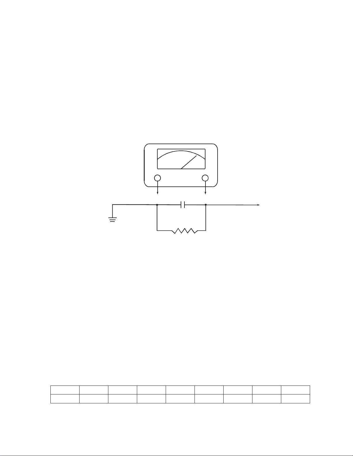
8) Before returning the set to your customer, always perform an AC leakage current check on the exposed
1
Page 4
metallic parts of the cabinet, such as antennas, terminals, screwheads, metal overlays, control shafts etc. to
A
be sure the set is safe to operate without danger of electrical shock. Plug the AC line cord directly into a
120V AC outlet (do not use a line isolation transformer during this check). Use an AC voltmeter having
5000 ohms per volt or more sensitivity in the following manner:
Connect a 1500 ohm 10 watt resistor, paralleled by a 0.15µF, AC type capacitor, between a known good
earth ground (water pipe, conduit, etc.) and the exposed metallic parts, one at a time. Measure the AC
voltage across the combination of 1500 ohm resistor and 0. 15µF capacitor. Reverse the AC plug at the AC
outlet and repeat AC voltage measurements for each exposed metallic part. Voltage measured must not
exceed 0.3 volts RMS. This corresponds to o.2 milliamp. AC. Any value exceeding this limit constitutes a
potential shock hazard and must be corrected immediately.
C VOLTMETER
¦Ì
0.15 FD
Good earth ground
such as a water
pipe, conduit, etc.
1500ohm
10watt
Place this probe on
each exposed
metallic part.
PRODUCT SAFETY NOTICE
Many electrical and mechanical parts in the chassis have special safety-related characteristics. These
characteristics are often passed unnoticed by a visual inspection and the X-RAY RADIATION protection
afforded by them cannot necessarily be obtained by using replacement components rated for higher wattage, etc.
Replacement parts which have these special safety characteristics are identified in this manual and its
supplement electrical components having such features are shaded on the schematic diagram and the parts list.
Before replacing any of these components, read the parts list in this manual carefully. The use of substitute
replacement parts which do not have the same characteristics as specified in the parts list may create shock, fire,
X-RAY RADIATION or other hazards.
B+ CHECK
1) Prepare the test equipment.
2) Use the DC voltameter at DC 200V position to test B+ test point, i.e. B+.
3) Connect the power plug to AC 120V/60Hz, turn on the power switch, wait for normal raster, Check B
100V±0.2V.
Test point B+ B1-5V B2-9V B3-10V B4-32V TH-12V TH-20V TH-200V
DC(V) 100 5 9 12 32 12 20(22) 200
+
=
2
Page 5
j
r
N
N
INSTALLATION AND SERVICE ADJUSTMENTS
GENERAL
In the majority of cases, a color television receiver will need only slight touch – up adjustment upon installation.
Check the basic characteristics such as FS,EHV,and focus. Observe the picture for good black and white details
without objectionable color shading. If color shading is evident, demagnetize the receiver.
If color shading still persists, perform purity and convergence adjustments. This should be all that is necessary
to achieve optimum receiver perfomance.
FOCUS ADJUSTMENT
Adjust the FOCUS control (on T302) for well defined scanning lines on the picture screen.
HIGH VOLTAGE CHECK
CAUTION: These is no HIGH VOLTAGE ADJUSTMENT on this chassis. Checking should be done following
the steps below.
1. Connect an accurate high voltage meter to the second anode of the picture tube.
2. Turn on the receiver. Set the BRIGHTNESS and CONTRAST controls to minimum (zero beam current).
3. High voltage will be measured below 9 (20”)KV.
4. Vary the BRIGHINESS control to both extremes to be sure the high voltage does not exceed the limit under
any conditions.
FS CIRCUIT CHECK
The Fail Safe (FS) circuit check is indispensable for the final check in the servicing. Checking should be done
following the steps below.
1. Turn the power switch on and adjust customer controls for normal operation.
2. Temporarily short TP501 and TP502 on the Main Board with a jumper wire. Raster and sound will
disappear.
3. The receiver must remain in this state even after removing the jumper wire. This is the evidence that the FS
circuit is functioning properly.
4. To obtain a picture again, temporarily turn the receiver off and allow the FS circuit more than 30 seconds to
reset. Then turn the power switch on to produce a normal picture.
Troubleshooting Guide for Fail Safe Circuit
3
Check that the set returns to normal operation when
pin 64 of N201 on the Main Board is grounded with
umper wire.
YES
Check if the voltage
across capacitor C551 is
approximately 17.2V
YES
Defective Fail Safe Circuit
O
Faulty
Power Circuit o
Horizontal Circuit
O
Page 6
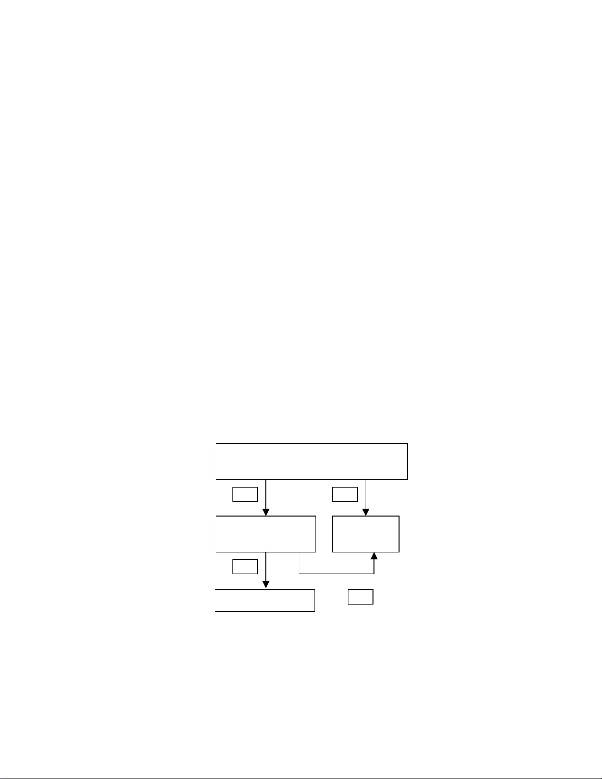
General instruction
1. This chassis’ EEPROMN801 M24C08 should copy standard data, if necessary, deal it with “factory
adjustment”. If directly use blank EEPROM, should first preset I
For factory adjustment method, refer to The appendix: factory menu.
2. If without special indication, the alignment is conducted on the below condition:
a) AC power supply 120 V/60 Hz.
b) The whole unit is preheated for more than 30 min.
3. There is built-in auto degaussing circuit, it will degauss automatically within 1second after turning on.
4. If CRT is with magnetism and affects color purity and convergence, the internal degaussing can not degauss
completely, can use degaussor to degauss externally. If color purity and convergence is still poor, then do
color purity and convergence adjustment.
2
C data, then go on other common alignment.
Alignment items and procedure
1. B+ voltage check
2. RF AGC voltage adjustment
3. Focus adjustment
4. Screen-grid voltage and white balance adjustment
5. Horizontal,vertical scan center adjustment
6. Horizontal,vertical scan amplitude adjustment
7. Pattern correction adjustment
8. The alignment flow chart see figure below.
EEPROM copy
B+ check
RFAGC adjustment
FOCUS
Screen-grid voltage
White balance adjustment
Scanning amplitude center &
raster correction adjustment
High voltage check
X-ray protection check
Filament voltage check
Picture and sound check
Sub-brightness check
White balance check
Color purity
convergence check
¡¢
AV term inal c heck
Check
The TV set & remote
controller's function check
Figure 1: Alignment flow chart
4
Page 7
Factory adjustment mode
1. B+ voltage test
a) Make sure the AC power is 120 V/60 Hz
b) Connect digital voltmeter to B+ test point, receive A-7 signal, set picture control to“MEMORY 2” state,
test B+, the test voltage should be 100 V±0.3 V.
2. AGC adjustment
a) Receive 60 dB split field A-7 signal.
b) Use oscilloscope or digital voltmeter to monitor test N201 pin 43 voltage(AGC output).
c) Press R-AGC button, by making use of [←][→] button, increase the value from low to high until the
voltage just reach 4.0 V, at this time picture noisy spot should basically disappear, otherwise continue
fine tune R-AGC button.
3. Focus adjustment
3. 1 Receive A-12 signal, set user control to “MEMORY 2” state.
3. 2 Adjust FBT’s focus potentiometer, to make the screen’s B area’s focus optimum.
4. Acelerating electrode adjustment method (use A-7 signal)
4.1 Roughly adjust white balance, fix RCUT value, adjust GCUT,BCUT,GDRV,BDRV’s value to make white
balance basically normal.
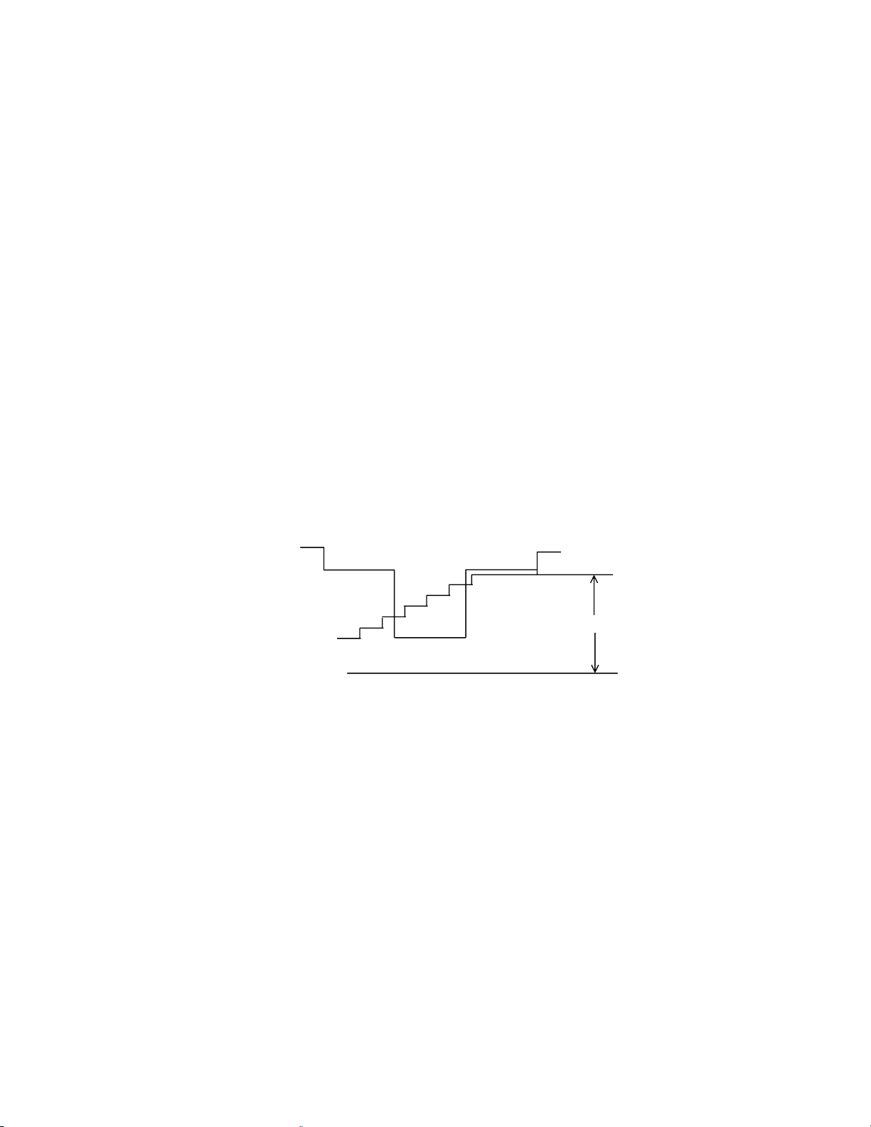
4.2 Set the color to 0, contrast to 30, use oscilloscope to adjust CRT’s red gun’s waveform (see below figure),
adjust brightness to make the seventh step’s (the darkest) DC level be 180V, adjust accelerating electrode to
make the seventh step slightly light up (just can separate the seventh step and below dark field).
0V
Fig 2: red gun waveform
4.3 Fine adjust white balance (color temperature: 12000K±8MPCD X=0.270±0.008 Y=0.283±0.008 )
4.4 Set contrast,brightness,color all to 0, adjust BRTN to make A-7’s upper left 2 lattice slightly light up.
5. Horizontal,vertical scan center adjustment
5.1 Item adjustment
VLIN 50Hz V-linearity adjustment
VSC 50Hz Vertical S-correction
VLIS 60Hz V-linearity adjustment
VSS 60Hz Vertical S-correction
5.2 PAL(50 Hz) H-center,V-center adjustment
Receive D35 signal, set user control to “MEMORY 2” state, fine tune V-center VP50, H-center HPOS,
to make picture’s center be in accordance with screen’s center.
5.3 NTSC(60Hz)H-center,V-center adjustment
Receive A6 signal, set user control to “MEMORY 2” state, adjust V-center VP60, H-center HPS to make
picture’s center be in accordance with screen’s center.
180V
5
Page 8

6. Vertical scan amplitude adjustment
6.1 PAL(50 Hz)V-amplitude adjustment
Receive D35 signal, set user control to “MEMORY 2” state, adjust V-amplitude HIT, make picture’s upper
and lower overscanning be screen size’s 8%.
6.2 NTSC(60 Hz)V-amplitude adjustment
Receive A 12 signal, set user control to “MEMORY 2” state, adjust V-amplitude HITS to make picture’s
upper and lower overscanning be screen size’s 8%.
Checking point
1. High voltage check
1.1 Connect high voltage meter to CRT’s second anode and GND.
1.2 Receive A-7 signal, set user control to “MEMORY 1” state, the high voltage should be 29.0 kV±1 kV.
1.3 When brightness and contrast be set to minimum (zero beam current), the high voltage should not exceed
32 kV.
2. CRT filament voltage check
Receive A-7 signal, set picture control to “MEMORY 2” state, use effective value voltmeter to test CRT
filament voltage, the reading should be (6.3±0.3)Vrms.
3. X-ray protection check
3.1 Receive A-7 signal, set user control to “MEMORY 2” state.
3.2 Short R554(TP501,TP502), X-ray protection circuit should effect.
4. Picture and sound check
4.1 Receive standard TV signal.
4.2 Making use of picture control buttons to check color,contrast,brightness,sharpness,tint’s control function.
4.3 Making use of sound control buttons to check volume control function.
5. Sub-brightness check
Receive A-7 signal, set color ,contrast,brightness all to 0, picture’s left side first grid slightly lights.
6. This set can produce 28 kinds of testing signal by itself. Press “SLEEP PIC DSP MENU AV” button,
every time you press the buttons, one kind of testing signal will be produced. The first fourteen signals
are NTSC signal and the other fourteen signals are PAL signal. After these signals are cycled for one
time, it will return to original screen.
7. Color purity and convergence check(Use common regulation)
8 . AV t e r m in als ( AV I N /OUT c h e c k )
9. Other control buttons (on the set and on the remote controller) function check.
6
Page 9
Preset the following in factory
1. Picture menu:
CONTRAST 100
BRIGHTNESS 50
COLOR 50
SHARPNESS 50
TINT ±00
PICTURE
MEMORY 4
MODE
▼MORE
2. Volume preset to 30.
3. Set OSD language to English.
4. Color system preset to AUTO.
5. TV mode:channel position number 2.
6. Firstly press SHOP OUT D/K SPOUT out-factory button on the factory remote controller,
“ready” will appear, wait for 8-10 seconds, the preset will be stored.
Factory menu
1. Enter into factory menu to operate.
1.1 Press “SLEEP PIC DSP MENU” button(The period of two-press should be within 5 seconds), enter into
factory menu.
1.2 Use MENU button to scroll the pages(P1,P2,P3).
1.3 In factory menu status, press SLEEP button to exit.
2. Factory menu contents(
OSD
No
.
01
02
03
04
05
charac
ter
RCUT
GCUT
BCUT
GDRV
BDRV
Pre
set
2F
4D
4B
41
45
06 HPOS 11 50Hz H-center MEMORY2 D35 screen
See below appendix 1.)
Appendix 1 Factory menu
Adjustment
Analogue
item
Dark area white
balance
Bright area
white balance
Contrast 0
Color 0
Bright 50
MEMORY1
setting
Input signal Adjustment methods Test point
Black/white
signal
Or
horizontal
Make dark area obtain
correct “white color”
screen
bright line.
Black/white
signal
Make dark area obtain
correct “white color”
screen
7
Page 10
07
08
09
10
11
12
13
14
15
16
17
18
19
20
21
22
VP50
HIT
VLIN
VSC
HPS
VP60
HITS
VLIS
VSS
RAGC
HAFC
V25
V50
TXCX
RGCN
ABL
06 50Hz V-center MEMORY2 D35
Adjust to make picture’s
vertical and horizontal
center be in accordance
with CRT center.
50Hz
25
V-amplitude
MEMORY2 D35
Cross-hatch
0B V-linearity MEMORY2
signal
(PAL)
Cross-hatch
signal
(PAL)
05
Vertical
S-correction
MEMORY2
03 60Hz H-center MEMORY2 A6 screen
Make V-amplitude meet
checking standard
screen
Adjust to make
screen’s upper and lower
cross-hatch height be
screen
equal.
Adjust to make screen’s
upper and middle and
lower cross-hatch
screen
height be equal.
Adjust to make picture’s
vertical and horizontal
03 60Hz V-center MEMORY2 A6
center be in accordance
screen
with CRT center.
60Hz
02
V-amplitude
60Hz V-linearity
00
02
29
03
42
4E
3F
16
23
fine tune
60Hz Vertical
S-correction
RF AGC
adjustment
1/2 AFC data
adjustment
25% volume
adjustment
50% volume
adjustment
YUV sub-color
maximum value
YUV sub-color
minimum value
Auto brightness
limitation
MEMORY2 A12
Cross-hatch
MEMORY2
signal
(NTSC)
Cross-hatch
MEMORY2
signal
NTSC
MEMORY2 A7
A12 Fix
A21 Fix
A21 Fix
Bright 50
Color 100
Contrast 50
Bright 50
Color 0
Contrast 50
In any
signal will
display
MENU
Let picture
without
color
MEMORY1 A7 fix Screen
To make V-amplitude
meet checking
screen
standard.
Adjust to make screen’s
upper and lower
cross-hatch height be
screen
equal.
Adjust to make screen’s
upper and middle and
lower cross-hatch
Screen
height be equal.
Adjust to make picture
without noise
Let character not
defocusing
N20143
Screen
Let character clear Screen
8
Page 11
23
24
25
26
27
28
29
30
31
32
33
34
35
36
37
38
DCBS
CNTX
CNTC
CNTN
SCNT
BRTX
BRTC
BRTN
BRTS
COLX
COLC
COLP
COLN
TNTX
TNTC
TNTN
BIT4, 5 OSD
character
brightness level
BIT2, 3
42
Ygamma value
BIT 0,1 black
level stretch
value
Sub-contrast
50
maximum value
Sub-contrast
3F
middle value
Sub-contrast
0F
minimum value
MEMORY1 Gray scale Fix Screen
Contrast 50 Gray scale Fix Screen
Contrast 0
Color 0
Gray scale Fix Screen
Bright 50
0F Sub-contrast Natural Gray scale Fix Screen
Sub-bright
1A
maximum value
Bright middle
2D
value
Sub-bright
20
minimum value
Contrast 50
Bright 100
A7 Fix Screen
Color 0
MEMORY2 A7 Fix Screen
Contrast 50
Bright 0
A7 Fix Screen
Color 0
Contrast 0
1C Sub-bright
Bright 50
A7 Fix Screen
Color 0
Sub-color
7F
maximum value
Sub-color
40
00
00
middle value
PAL sub-color
middle value
Sub-color
minimum value
Contrast 50
Bright 50
Color 100
Natural A7 Fix Screen
Natural D8 Fix Screen
Contrast 50
Bright 50
Color 0
D8
A7
Fix Screen
A7 Let picture without color Screen
Contrast
50
Sub-tint
maximum
value
100
Bright 50
Color 50
A7 Fix Screen
Tint 100
Sub-tint middle
50
50
value
Sub-tint
minimum
Natural A7 Fix Screen
Contrast
100
A7 Fix Screen
9
Page 12

39
40
41
42
43
44
45
46
47
48
49
50
TNCD
SHPX
SHPN
ST3
SV3
ST4
SV4
SVD
DEF
STBY
ASSH
VBLK
value Bright 50
Color 50
Tint 0
Contrast
DVD Tint
40
middle value
100
bright 50
Color 50
Tint 0
Sub-sharpness
3F
maximum value
Sub-sharpness
10
minimum value
Sharpness
100
Sharpness 0 A12 Fix Screen
NTSC3.58 TV
input signal’s
2E
sharpness
MEMORY1
middle value
NTSC3.58 AV
input signal’s
2E
sharpness
MEMORY1
middle value.
Non NTSC3.58
TV input
2E
signal’s
MEMORY1 A12, B12 Fix Screen
sharpness
middle value
Non NTSC 3.58
AV input
2E
signal’s
MEMORY1
sharpness
middle value.
DVD sharpness
19
middle value
Fix Screen
0:picture
parallel
01
1:picture
non-parallel
Decoder
intermediate
00
amplifier
STANDBY
Single side
00
sharpness
Vertical
blanking
00
beginning point,
ending point.
DVD Fix Screen
A12 Fix Screen
Video input
NTSC3.5
Fix Screen
signal
Video input
NTSC3.5
Fix Screen
signal
Video input
PAL sign al
Cross-hatch
signal
Fix Screen
Fix
10
Page 13

MOD
51
03 Mode data
Chroma
UCOM
52
00
auto-phase
control setting
NOIS
53
54
55
SYCT
TUNR
01 Noise check
Sync signal
08
check
02 Tuner selection
CCD(concealed
56
CCD_
OSD
caption) OSD
50
beginning
position
57
58
59
60
61
62
CCD_
OSDF
OSDF
OSD
OPT
OPTM1
OPTM2
CCD character
50
size
OSD character
4F
size
15 OSD position
07
A3
13
Note 1:The original password CHILD LOCK MENU 0000,
VCHIP PASSWORD 0000.
CONVERGENCE MAGNET ASSEMBLY POSITIONING
Convergence magnet assembly and rubber wedges need mechanical positioning. Refer to below figure 1.
COLOR PURITY ADJUSTMENT
NOTE: Before attempting any purity adjustment, the receiver should be operated for at least fifteen minutes.
1. Demagnetize the picture tube and cabinet using a degaussing coil.
2. Set the CONTRAST and BRIGHTNESS controls to the maximum.
3. Receive PM5515 monochromatic signal (such as G) to provide a green raster on the screen.
4. Loosen the clamp screw holding the yoke, and slide the yoke backward to provide vertical green belt
(zone) in the picture screen.
5. Remove the Rubber Wedges.
6. Rotate and spread the tabs of the purity magnet around the neck of the picture tube until the green belt
is in the center of the screen. At the same time, center the raster vertically by adjusting the magnet.
7. Move the yoke slowly forward or backward until a uniform green screen is obtained. Tighten the
clamp screw of the yoke temporarily.
8. Check the purity of the red and blue raster.
9. Obtain a white raster, referring to “CRT WHITE BALANCE ADJUSTMENT”.
10. Proceed with convergence adjustment.
11
Page 14

FIG.3
CONVERGENCE ADJUSTMENT
NOTE: Before attempting any convergence adjustments, the receiver should be operated for at least fifteen
minutes.
CENTER CONVERGENCE ADJUSTMENT
1. Receive crosshatch pattern with a color bar signal generator.
2. Adjust the BRIGHTNESS and CONTRAST controls for well defined pattern.
3. Adjust two tabs of the 4-Pole Magnets to change the angle between them (see figure 4) and superimpose red
and blue vertical lines in the center area of the picture screen. (see figure 5)
4. Turn the both tabs at the same time keeping the constant angle to superimpose red and blue horizontal lines at
the center of the screen.(see figure 5)
5. Adjust two tabs of 6-Pole Magnets to superimpose red/blue line with green one. Adjusting the angle affects
the vertical lines and rotating both magnets affects the horizontal lines.
6. Repeat adjustments 3,4,5, keeping in mind red, green and blue movement, because 4-Pole Magnets and
6-Pole Magnets interact and make dot movement complex.
CIRCUMFERENCE CONVERGENCE ADJUSTMENT
1. Loosen the clamping screw of deflection yoke to allow the yoke to tilt.
2. Put a wedge as shown in figure 1 temporarily. (Do not remove cover paper on adhesive part of the wedge.)
3.Tilt front of the deflection yoke up or down to obtain better convergence in circumference. (See figure 5).
Push the mounted wedge into the space between the picture tube and the yoke to hold the yoke temporarily.
4. Put other wedge into bottom space and remove cover paper to stick.
5. Tilt front of the yoke right or left to obtain better convergence in circumference (see figure 5)
6. Keep the yoke position and put another wedge in either upper space. Remove cover paper and stick the wedge
on the picture tube to fix the yoke.
7. Detach the temporarily mounted wedge and put it in another upper space. Stick it on the picture tube to fix the
yoke.
8. After fixing three wedges, recheck overall convergence. Tighten the screw firmly to fix the yoke tightly in
place.
12
Page 15

9. Stick three adhesive tapes on wedges as shown in figure 3.
Fig5. Dot Movement Pattern
13
Page 16

BAN
D
VHF
Low
VHF
High
USA CHANNEL FREQUENCY TABLE (181 CH)
P IF=45.75 MHz
C IF=42.17MHz
S IF=41.25MHz
UNIT: MHz
CHANNE
L
W+1
W+2
W+3
W+4
W+5
W+6
W+7
W+8
W+9
W+10
P
CARRIER
2 55.25 59.75 101
3 61.25 65.75 107
4 67.25 71.75 113
5 77.25 81.75 123
6 83.25 87.75 129
A-6
A-5
A-4
A-3
A-2
A-1
A
B
C
D
E
F
G
H
I
7 175.25 179.75 221 15 477.25 481.75 523
8 181.25 185.75 227 16 483.25 487.75 529
9 187.25 191.75 233 17 489.25 493.75 535
10 193.25 197.75 239 18 495.25 499.75 541
11 199.25 203.75 245 19 501.25 505.75 547
12 205.25 209.75 251 20 507.25 511.75 553
13 211.25 215.75 257 21 513.25 517.75 559
J
K
L
M
N
O
P
Q
R
S
T
U
V
W
S
CARRIER
85.25 89.75 131
91.25 95.75 137
97.25 101.75 143
103.25 107.75 149
109.25 113.75 155
115.25 119.75 161
121.25 125.75 167
127.25 131.75 173
133.25 137.75 179
139.25 143.75 185
145.25 149.75 191
151.25 155.75 197
157.25 161.75 203
163.25 167.75 209
169.25 173.75 215 14 471.25 475.75 517
217.25 221.75 263 22 519.25 523.75 565
223.25 227.75 269 23 525.25 529.75 571
229.25 233.75 275 24 531.25 535.75 577
235.25 239.75 281 25 537.25 541.75 583
241.25 245.75 287 26 543.25 547.75 589
247.25 251.75 293 27 549.25 553.75 595
253.25 257.75 299 28 555.25 559.75 601
259.25 263.75 305 29 561.25 565.75 607
265.25 269.75 311 30 567.25 571.75 613
271.25 275.75 317 31 573.25 577.75 619
277.25 281.75 323 32 579.25 583.75 625
283.25 287.75 329 33 585.25 589.75 631
289.25 293.75 335 34 591.25 595.75 637
295.25 299.75 341 35 597.25 601.75 643
301.25 305.75 347 36 603.25 607.75 649
307.25 311.75 353 37 609.25 613.75 655
313.25 317.75 359 38 615.25 619.75 661
319.25 323.75 365 39 621.25 625.75 667
325.25 329.75 371 40 627.25 631.75 673
331.25 335.75 377 41 633.25 637.75 679
337.25 341.75 383 42 639.25 643.75 685
343.25 347.75 389 43 645.25 649.75 691
349.25 353.75 395 44 651.25 655.75 697
355.25 359.75 401
LOCAL BAND CHANN
EL
W+11
UHF
W+12
W+13
W+14
W+15
W+16
W+17
W+18 403.25
W+19
W+20
W+21
W+22
W+23
W+24
W+25
W+26
W+27
W+28
W+29
45 657.25 661.75 703
P
CARRIER
S
CARRIER
361.25 365.75 407
367.25 371.75 413
373.25 377.75 419
379.25 383.75 425
385.25 389.75 431
391.25 395.75 437
397.25 401.75 443
409.25 413.75 455
415.25 419.75 461
421.25 425.75 467
427.25 431.75 473
433.25 437.75 479
439.25 443.75 485
445.25 449.75 491
451.25 455.75 497
457.25 461.75 503
463.25 467.75 509
469.25 473.75 515
LOC
AL
407.75 449
14
Page 17

USA CHANNEL FREQUENCY TABLE (181 CH)
P IF=45.75 MHz
C IF=42.17MHz
S IF=41.25MHz
UNIT: MHz
BAND CHANNEL P CARRIER S CARRIER LOCAL
UHF
46 663.25 667.75 709
47 669.25 673.75 715
48 675.25 679.75 721
49 681.25 685.75 727
50 687.25 691.75 733
51 693.25 697.75 739
52 699.25 703.75 745
53 705.25 709.75 751
54 711.25 715.75 757
55 717.25 721.75 763
56 723.25 727.75 769
57 729.25 733.75 775
58 735.25 739.75 781
59 741.25 745.75 787
60 747.25 751.75 793
61 753.25 757.75 799
62 759.25 763.75 805
63 765.25 769.75 811
64 771.25 775.75 817
65 777.25 781.75 823
66 783.25 787.75 829
67 789.25 793.75 835
68 795.25 799.75 841
69 801.25 805.75 847
15
Page 18

WIRING DIAGRAM
X302
782-13Y00-05
S501
782-K2035-01
FBT
782-K2035-05
X90-1
X301
X202
N201
Xv02
X601
X201
Xv11
X90-1
X302
782-K2035-02
X401
16
Xv11
782-K2035-29
Xv02
Page 19

A
A
BLOCK DIAGRAM
AC 120V
ROUT
B+100V
B+ 100V
B29V-1
BSC24-3031
DB501
B15V-1
FBT
POWER
B432V
AUDIO OUT
N601
AN7522N
RIN
ON/OFF
X-R
D
LIN
TC4052
N5832
RMIN
POWER
EEPROM
M24C08BN6
N801
N501
B312V
TH-12V
TH-20V
TH-200V
VOUT
17
V323
HOUT
TEA8172
R
G
B
TUNER
CRT
Page 20

IC BLOCK DIAGRAM
P61/LED1/ADC8bit
P60/ADC8bit
P53/ADC8bit/TC1/Int2
uP Dvss
Reset
8MHz
TEST
uP DVDD 5V
uP VVss
TV AGND
FBP
SCP
HAFC1
Vsaw
Vout
H.Vcc 9v
TV DGND
EXT CVBS/Y
Dvcc
TV IN 1Vpp
TRAP
IF Vcc 9V
TVout 2.2Vpp
SIF out
TMPA8801PSN(PN)
8-bit int.timer 2
Watchdog timer
interrupt
Ext. 5 Int. 11
IIC bus interfece
XO
Ext. 1 Int. 1
¡Á¡Á
¡Á¡Á
¡Á
STOP/IDLE mo de
Hor.Proc.
Sync.sepa
Hor.VCO HAFC-1
RGB Matrix
Vert.Proc.
V.C /D
V.r am p
Y gamma
Sharpness
ATT
1
2
3
4
5
6
7
8
+
9
10
11
HAFC-2 H-shift
12
13
Hout
14
+
V.geometry
V.D ri ve
15
16
17
++
18
19
Cb input
20
Y input
21
Cr input
22
23
Cin
24
+
25
26
27
ABCL
28
AU out
29
+
30
31
32
+
EXT AU
16-bit int.timer 2
¡Á
870
¡Á
CPU core
Color Uni-color
Black stretch
Romote preprocessor
CCD
C-Trap
8-bit ADC Ext 3
I/O
10 I/O port
14-bit PWM 1
7-bit
¡Á
PWM 1
Int. 1
¡Á
¡Á
¡Á
ROM:64kB
RAM:2KB
ROM correction
OSD R/G/B/Ys/I
Font:16
Display:32C 12L
Color:8
Character:384
Half-tone Test signal
Transparent
¡Á
18
¡Á
Base Band Pr c.
1H DL Int/Ext switch
o
Chroma Proc.
C-BPF
PAL/ NTSC
TINT
Y Proc.
AGC
AGC
DET
Reg.
PIF Proc.
PAL/NTSC demod
Auto.VCO
alignment
AFT
64
63
62
61
60
59
58
57
56
55
54
53
52
Cut-off Drive
AKB
51
50
49
48
47
46
45
44
43
42
IF
41
40
39
38
37
FM
DEMO
36
35
34
BPF
33
P63/LED2
P30/Int3/RXIN
P31/Int4/TC3
P20/Int5/Stop
P40/PWM14bit
P50/PWM7bit/TC2/Int0
P51/SCL
P52/SDA
P56
uP AVdd 5V
+
uP MPAGND
TV AGND
Bout
Gout
Rout
+ +
RGB Vcc 9V
IKin
APC Fil
+
Black Det
Monitor out
+
YC Vcc 5V
F AGC
R
IF IN
SAW
IF GND
++
IF AGC
Deemph
S-Reg.F
IF Vcc 5V
+
PIF PLL
+
DC NF
H.correc/SIF in
18
Page 21

10K
10K
£©
(Ta
10
3.3
£©
(Ta
3.3
0.1
¡À£©
(10%
0.022
AN5832SA
180K
PE
26
2.2
24
+
32
SDA/SAPID
SCL/STID
27
Wide Band
2
IC
Decoder
+
+
2
3
Spectral
Filter
Filter
+
5
6
4
10% Tantalum capacitor
(Ta)
28293015251917182321
Spectral
Wide Band
Wide Band
RMS Det
Expand
2.2
Lout Rout
2.2
+
GND
AGC
Matrix
& Mode SW
Offset
Cancel
Offset
Cancel
L-R
L+R
Filter
75 s
Filter
De-Emph
SAP out
5V
VCC
Pilot Det
+
0.33
PLL
Pilot
Cancel
SAP
RMS Det
Spectral
Expand
Dbx
De-Emph
(L-R)/SAP
Switch
Filter
0.1
Demod
Noise
Det
13
SIF
Base Band
0.22
Input
Input
0.1
2.2 2.2 2.22.2
4.7
3.3K
+++++
1000P
+
SIF
22
Demod
Input
Offset
Cancel
VCA
4.7
19
SIF/BB
Stereo
Filter
SAP
SW
7
8
AGC
2
IC/PARA
Mode Control SW
SAP
Det
Filter
9
MODE
10
FOMO
Noise
Filter
11
MUTE
14
0.033
12
SIF/BB
Page 22

1D
S
2
VIN1
+
-
O.C.P/F.B
5
VIN2
GND
3
-
+
STR-G5653
O.S.C
Vin
4
START O.V.P LATCH DRIVE
REG
+
-
T. S . D
ERROR AMP
20
Page 23

TEA8172
Amplifier
1
-
Power
7
+
4
Flyback
Thermal
Protection
Generator
362
5
21
Page 24

AN7522N
11 12
10
22
3 4 5 6 7 8 9
2
1
Vcc GND
Page 25

THE IC PIN’S VOLTAGE IN NORMAL/STAND BY WORKING MODE (120V, PRESENT
MODE)
1. TMPS8801(N201)
PIN Vlotage(V)
Normal
Voltage (V)
Stand by
PIN Voltage(V)
Normal
Voltage(V)
Stand by
1 5.69 5.63 33 3.04
2 5.69 5.62 34 2.55
3 5.68 5.61 35 2.48
4 0 0 36 5.20
5 5.69 5.62 37 2.25
6 2.52 5.60 38 4.5
7 2.29 2.49 39 1.77
8 0 2.26 40 0
9 5.69 5.60 41 0.10
10 0 0 42 0.10
11 0 43 2.11
12 1.06 44 5.19
13 1.81 45 1.84
14 6.81 46 2.46
15 4.21 47 2.66
16 5.03 48 1.37
17 9.19 49 1.37
18 0 50 9.23
19 2.56 51 2.41
20 2.57 52 2.48
21 2.56 53 2.59
22 0 54 0 0
23 0 55 5.70 5.60
24 2.55 56 0.06 5.56
25 3.52 57 5.33 5.54
26 2.77 58 5.23 5.50
27 4.71 59 0.01 0
28 3.60 60 2.20 5.56
29 9.24 61 0 0.04
30 3.73 62 5.04 5.50
31 1.91 63 5.64 5.55
32 0 64 0 1.04
23
Page 26

2. AN5832(NS01)
4. TEA8172(N301)
PIN Voltage(V) PIN Voltage(V)
1 Empty 17 3.23
2 0.73 18 3.58
3 2.76 19 5.20
4 0.60 20 Empty
5 2.45 21 3.67
6 2.03 22 3.48
7 5.20 23 2.25
8 Empty 24 5.14
9 Empty 25 0
10 Empty 26 Empty
11 Empty 27 4.90
12 Empty 28 1.89
13 3.45 29 2.22
14 3.46 30 2.22
15 2.28 31 Empty
16 Empty 32 2.12
PIN Voltage
1 3.75
2 20.6
3 1.53
4 0.01
5 12.86
6 20.9
7 3.76
5. STR-G5653(N501)Voltage(V)
PIN 1 2 3 4 5
Standby 135 0 0 20 0
Voltage 18 0 0 32 5
3. AN7522N(N601)
PIN Voltage(V)
1 10.52
2 4.66
3 0
4 4.68
5 8.18 0.44
6 1.49
7 0
8 1.48
9 0.43
10 4.62
11 0
12 4.61
6. TC4052(TV)
PIN Voltage PIN Voltage
1 4.30 9 0.05
2 0.27 10 0.01
3 0.75 11 0
4 Empty 12 0.74
5 0.22 13 0.74
6 0 14 0.6
7 0 15 0.13
8 0 16 9.23
7. TDQ-3B8GN(A101)
1 3 4 5 6/7 9 11
AGC AS SCL SDA BM1/2 BT IF
2.1 5.0 5.7 5.3 5.03 32 0
24
Page 27

The triode pin’s voltage in normal working mode (120V, PRESENT Mode. Parenthesis
means stand by)
Symbol Type
Voltage
C E B
V101 2SC2717 7.38 0.24 1
V206 C1815Y 9.23 1.97 2.59
V207 C1815Y 9.23 1.85 2.48
V208 C1815Y 9.23 1.79 2.41
V401 2SC2688 164.6 1.46 1.77
V402 2SC2688 161.4 1.53 1.84
V403 2SC2688 156.4 1.64 1.95
V404 2SC1815Y 2.81 0.01 0.01
V801 2SA1015 0 2.52 1.84
V802 2SA1015 2 9.16 9.18
V803 C1815 4.95 0 0.24
V810 A562TM-0 5.7 5.71 5.03
V601 C1815-Y 0.55 0 0
V509 2SA1015 0 13.06 13.13
V508 SFORIB42 0.01 0.03 0.01
V201 C1815Y 9.24 3.02 3.72
V205 2SA1015Y 0 3.75 3.07
VV01 2SA1015 0 0.7 0.03
V203 C1815Y 9.24 3.68 4.34
V501 2SA1015 9.89(7.41) 13.14(7.56) 12.56(6.77)
V502 2SC1815-Y 12.56(0) 0.01(0) 0.03(0.68)
V505 2SC3807 13.14(7.5) 9.21(0) 9.77(0.13)
V507 2SC3807 9.89(7.3) 5.72(5.5) 6.26(6.0)
V506 2SC1815-BL 9.77(0.2) 0.01(0) 0.03(0.7)
V324 C3807 7.03 5.33 5.89
V322 C2383-0 21.2 0.01 0.4
N303 78M09 13(1 Pin) 0(2Pin) 9(3Pin)
25
Page 28

CAUTION: All the parts in the schematic
diagram marked with red frame and the signs
of are extremely important a safety. In case of
replacement of any part of the components. Be
sure to consult the service manual carefully.
1. The schematic diagram is characteristic. The
various values in the electric circuits are
basic data, which are changeable
according to the various basic circuits.
2. Testing waves are obtained by inputting the
standard color bar of the signed.
3. Resistance unit is in Ohm, namely:
K=1000 M=1000K
Capacitance unit is in F.
P= F( =10
-6)
4. Unless otherwise noted inside, all resistors
are 1/6W, the withstand voltage of all
capacitor are 50V.
5. Inductance unit is in H.
6. The mark in the diagram means Ferrite
ring.
7. The symbols of various types of resistors and
capacitors are listed as follows:
Carbon Film
Metal Film
M
Potentiometer
1/2W
1W
2W
3W
1
2
3
Ceramic
AC Ceramic
AC
Ployester
Ploypropylene
Metal Polyester
Aluminium
Tantalum
+
+
T
Page 29

16151413121110987654321
NTSC
2001.11.26
9V-2
GND
KILL
SPOT KILL
D
X901
1 5
REMO IN
GND
+5V
12V-2
KEY
C
XV11
GND
1 5
*
1
2
10
XV10
11
3
2200U
V IN
4
XV09
GND
A IN R
A IN L
1
GND
XV08
Y
XV07
XV06
X601
B
A
+
_
_
+
X501
LN
AC
N
L
R
W
4
1
N
L
L OUT +
L OUT -
R OUT -
R OUT +
C610
100P
LV06
10uH
LV05
10uH
GND GND GND GND
C611
100P
100n400V
CV1610uF
5698
4
CV15
16V 10uF
CV10
100P
GND
CV09
GND
C611
100P
C508
4n7 250V
2
C506
4n7 250V
C505
V801
2SA1015
R815
R814
560K
680
C809
50V F1u
LED901
*
RC901
3
2
1
RECEIVER
GND
S906
MENU
RV23150
GND
7
RV22
150
10K
RV20
GND
RV19
100P
10K
GND
C613
100P
DB501
T2SB60
1
4
R502
5D2-14LC
1
3
2
t
C504
RT501
470P
9
C502
AC250V 0.1u
T501
LF210-65
C501
AC250V 0.22uF
R501
2M2
R811
2.2K
R812
100
R816
68K
R901
270
GND
C901
R907
120K
S905
TV/AV
L OUT +
4n7 250V
4n7 250V
FU501
T2.5A/AC250V
R810
470
R813
3.3K
GNDGND
C808
CH180
V802
2SA1015
R817
12K
GND GND GND
GND
16V 47uF
R906
30K
S904
VOL-
R OUT +
C509
3
C507
C503
470P
GND
R818
3.9K
12V-2
5V-1
R905
18K
680P 2K
B. G. R.
C807
16V 33uF
GND
C810
B1500
C522
0.01 1KV
C513
R902
47
S903
VOL+
2SA966
RBG
MONITOR
C811
B1800
REMO IN
R904
12K
V509
RL501
JQX-115F
2
1 5
LF21065
1N4148
T502
1 6
X201
V803
C1815
R819
3.9K
KEY
R903
5.6K
S902
CH-
R610
12K
VD601
C549
4.7uF
GND
C548
470uF16V
4
220uF/250V
D
S
2 1
R508
0.15 2W
GND
X903
1
S901
CH+
MUTE
SPOT KILL
GND
VD509
1N4148
R549
10K
VD506
IN4148
GND
C510
C511
100n 400v
N501
STR-G5653
Cont
Block
VD505
IN4148
R507
680
10
GND
VD602
IN4148
R609
12K
R511
10 1/4W
FB/OCP
GND
16V 10uF
C240
100
GND GND
TV/AV
8M
Gnd in
7
GND
C606
10uF
*R606
GND GND
C826
100P
SCL
C239
100
SCL1
X-TAL
6
47
VD803
HZ4B1
R860
220
2K7
SDA
GND
C824
16V 10u
GND
Ch.2 in
8
L601
1mH
GND
C827
100P
SDA1
TEST
GND
C604
GND
R808
10K
R809
10K
5V-1
R820
10K
R867
10K
C802
C825
L802
12uH
Vol10Ch.2 out-11Gnd12Ch.2 out+
9
C605
10uF
C603
10uF
N801
45
SDAGND
3
6
SCL
A2
TEST
A1
A0
M24C08BN6
C804
1K
RMT IN
POWER
PW
STAND-BY
R850
R851
100
100
R854
R853
10K
10K
2
1
A/B
33V
Ch.1out+
23
L OUT +
27P
GND
WP
7
8VCC
R805
27K
R804
10K
GND
TV SYNC
KEY
R852
1K
R855
33K
GND
A562TM-0
Gnd
4
R604
L OUT -
R807
GND GND
47
C806
0.01
C607
A
16v47uF
R801
1K
GND
VOL
AV SW
GND
RESET5VX-TAL
10n
C821
C82247C823
R856
470
RESET
V810
Stand by
Ch.1out-
5
R601
C602
100K
10uF
GND
GND
47K
C805
B
G801
R861 4K7
R859
1K5
Ch.1 in
6
2
1
GND
5V-1
R822
10K
R803
2
12345678910111213141516171819202122232425262728
C820
0.01
GND
5V-1
R866
10K
GND
X202
VOL
V601
C1815-Y
GND
R548
220
12V-2
R607
10K
N601
AN7522
C601
25V 2200uF
VOL
Vcc
1
GND
12V
N502
TLP621GP
1 2
3
4
R505
1/2W-1M
4
5
C514
47uF/50V
R504
C515
470P
220K 1W
5K6
VD501
S5295J
IN4148
HZ16-1
VD502
VD503
VD504
IN4148
R503
Vin
3
POWER
R510
1K8
T503
1
9
2
R518
5M6
C521
2200 AC250V
8
12
11
10
13
14
GND
18
4
3
R512
47
6
RP501
100
R506
1K
5
C516
1200P
7
VD530
TRU3A
C530
330P 2KV
GND
VD532
TFR155
C532
330P 500V
VD533
TFR155
C536
330P 500V
GND
VD534
TFR155
C540
330P 500V
GND
180V 470uF
XITP
R536
1/2W 1
C542
R537
1/2W 1
C543
.1
R538
1W 0.47
C544
.1
VD531
HZ6C2
C531
GND GND
1
GND
2
.1
GND
C537
1000uF/16V
C541
2200uF25V
SCHEMATIC DIAGRAM
B.WPG. R.
789
R212
200
V208
C1815Y
R208
150
51
G OUT
H-AFC
C221
0.47uF 50V
Ch.2 in (R)
C609
10n
R532
4.7 1W
V501
22K
C534
1000uF 16V
GND
B1-5V
C539
.01
200
R213
M
C222
GND
Ch.1 in (L)
2SA1015
B2-9V
10V
1K
GND
C214
R207
150
R OUT
V-SAW
0.47
C535
GND
16V 100u
C223
VOUT
H SYN
.01
L202
12uH
C215
0.01
GND
C213
C212
0.22uF
B2200
GND
GND
30K
33K
R206
R246
1KIN
APC FIL
RGB VCC(9V)
V-OUT
H-VCCNCCb
C224
C2251uC2261uC227
.01
1000uF
GND GND
L203
R222
12uH
1K
GND
R309
15K
3
B4-32V
R545
15K 2W
H VCC
9V
X-RAD
B+
R542
4K7
GND
V506
2SC1815-BL
GND
C211
1u
R205
220K
BLACK DET
R223
CbYCr
100
2
5V-1
110V
R541
4K7
L209
12uH
C210
R224
100
SFORIB42
R868
M1962M
GND
C209
100uF
0.01
GNDGND
RF AGC
YC VCC
MONITOR OUT
Y-INCrTV-GND
R256
100
1u
GND
R225
100
C256
B2200
IDENT
R552
V508
2K7
GND GND GND
C550
1K
0.01
R311
R310
GND
0.01
MUTE
0.01
10n
R OUT -
R530
GND
C533
100uF
8V
GND
12uH
5V
GND
GND
5V-1
R602
GND
15K2W
8V
R547
C547
16V10uF
L801
R531
220
R214
1K
1K
R215
GNDGND
C1815Y
C801
16V 10u
GND
GND
GND
R220
10K
10K
R OUT +
GND
L501
75uH
V502
2SC1815-Y
R546
7501W
C546
GND
V507 2SC3807
1K
GND
L502
100uH
R210
R211
200
V206
V207
C1815Y
R209
150
GND
52535455565758596061626364
GND
B OUT
N201
TMPS8801PSAN
FBP-IN
SCP-OUT
H-OUT
C220
B8200
R221
8.2K
SDA/SCL
Y/C
H SYN
4
H OUT
10K
R603
C608
10n
GND GND
R533
6K8
GND
R534
V505
2SC3807
VD507
HZ9C3
GND
25V47uF
VD508
HZ6B1
C538
330uF16V
B3-10V
Z201
3215
4
R204
820
IF IN
C-IN
R226
100
C228
C IN
VD561
HZ18-3
10K
3K9
GND
C310
47uF/16V
L201
12uH
IF IN
EXT-IN
GND
C229
0.47uF
10uF
1/2W 270
Y IN
TP502 TP501
R553
30K
C305
1000p
IF GND
DVCC 5V
C230
0.01
C231
0.47u
R227
R554
10K
input
Non inv
GND
GND
GND
C232
C208
0.01
C205
C233
0.1
R228
390K
1
0.1
Vcc
Out Stage
C207
16V 470u
GNDGND
4.7uF 50V
M
1uF
IF-AGC
TV IN
M
M
GND
17.2V
N301
V out
C302 10P
220uF 35V
R305
33K
R302
12K
R108
220
C204
M
C206
0.01uF
DEEMPH
ABCL-IN
C234
10u
GND
C235
VD204
1N4148
11
GND
ABL
TEA8172
Gnd
GND
VD301
TVR-1B
C303
R307
200
R306
10K
C306
4.7uF/50V
GND
C109
0.01
L103
0.68uH
GND
C108
0.01
R202
C203
100
1000P
C202
R203
1.5M
S-REG
IF-VCC
PIF PLL
AUDIO-OUT
IF-VCC(9V)
TV-OUT
29 30 31 32
GND GND
GND
C236
0.01
10u
R230
100
GND
L208
12uH
R229
3.3K
TV IN
Y CB CR
H-OUT
EXT IN
9V-2
R243
1K
R244
1K
J079
Vcc 1
Flyback
20V
C301
1n
C308
0.1
M
C307
1000u 35V
R303
*1.2 1W
GND
2SC2717
R201
330K
0.47u
R242
3K3
V201
C1815Y
Inv in
1234567
GND
M
GND
R106
270
V101
R107
33
C201
16V 10u
333435363738394041424344454647484950
DC-NF
SIF-OUT
9V-2
GND
C351 0.1
GND GND
R308
1
C309
0.1
X301
R104
5.6K
R105
1K
GND
SIF-IN
EXT-AUDIO
C238
R231
0.01
100
R240
R241
390
330
2SA1015Y
R237
100
L204 10uH
R236
220
C350
220uF 35V
11
C107
0.01
L102
0.56uH
C246
0.01
Z203
LT4.5M
GND
GND
R233
27K
TV/AV/L/R
V205
GND
XT4.5MB
GND
12V-2
R312
R316/R317
GND
R314
R315
GND
3456 12
5V-2
9V-2
VT
A101
R103
100
C560
1000
GNDGNDGND
GND
C243
V203
0.01uF
C1815Y
R232
27K
GND
R235
R234
1K
1K
GND
GND
R239
2K2
R238
1K
Z202
C311
GND
220uF25V
TH-20V
5V-2
1W 150
GND
C344
0.01
1000uF 35V
1W 150
18K
1K
R320
330
R322
330
C2383-0
GND GND GND
IF
C561
50V 10u
GND GND
33V
C3807
C341
GND
V322
IF
1011
N505
uPC574JL
C244
16V 47uF
GND
RV01
LV07
100uH
CV13
0.1
C551
50V10u
GND
C557
.01
GND
V324
GND
C343
470uF 16V
C346
0.01
GND
C322
1n 500V
782-K2035-0100
M
CS08
1
SIF IN
XS01
GND
GND
5V-2
R216
SDA
100
SCL
R217
GND
RV16
C349
GND
C329
4u7 160V
S5295J
C330
390n 200V
GND
75
RV05
GND
RV04
GND
IDENT
LV04
10uH
LV03
10uH
100P
R328
1W10K
CKX5-2K-2
GND
RV21
Y
Cb
Cr
CV12
100P
10K
GND
CV11
10K
GND
HEATER
8
7 6 5
75
A IN L
A IN R
LV02
10uH
LV01
10uH
200V
100
GND
L IN
L IN
R IN
R IN
8
GND
Y
2 1
9 10
XV05
4 3
C
3
XV03
1
*
GND
XV02
1
L IN
R IN
GND
V IN
4
V-IN
XV01
6
L1
A-IN L
7
1
R1
A IN R
3
18
V1
V-IN Y
19
15
Y
17
75
RV13
GND
8
Cb
75
RV12
GND 9
4
Cr
75
RV11
GND
5
10
L2
11
12
R2
13
14
GND
4
667-K2035-0200
GND
1
X302
1 6
X401
R
G
B
9V
GND
GND
AS
SCL
SDA
C106
0.01
89
GND
16V 470uF
7
C105
GND
BM2
6
BM1
L101
68uH
AGC
AGC
3
R109
100
R102
15K
R101
62K
12
C102
50V 4.7u
GNDGND
4
5
R110
100
SCL
SDA
BT
5V-2
9V-2
RV17
2.2K
RV18
1K
GND
VV01
2SA1015
SIF IN
5
SIF IN
CV08
100P
10K
RV15
GND
GND
CV07
100P
10K
RV14
GND
GND
SDA/SCL
5V-2
R IN
L IN
9V-2
L IN
CV03
CV04
10uF
1000u/16V
C324
CV05
100uF
GND
C556
GND
VD342
TFR155
1n
GND
NV01TC4052
10
A
11
3X
0X
12
XC
13
1X
14
2X
15
16 0Y
VDD
C333
VD302
5600
5.1V
GND
TH-12V
C347
330P 500V
V323
D1651
C325
4n7 1K6V
VSSB
VEE
INH
1Y
3Y
YC
2Y
GND
C348
33uF 160V
C326
*6n81K6V
GND
89
7
6
5
4
3
2
1
R333
6.8K
330P 500V
C352
GND GNDGNDGND
GND
R IN
R313
6.8K
VD343
R350
1W 1
R351
1W 1
R343
1W 10
GND
C327
*820P 2KV
TFR155
12
13
TH-200V
100V
CV01
10uF
CV02
10uF
Ch.2 in (R)
10K
RV10
RV07
RV08
CV06
5K6
16V 10u
100K
RV09
5K6
GND GND
RV06
100K
10uF/250V
R555
T302
1 1W
5
HV
3
8
GND
4
2
1
6
10
L333
*HL1830H
R326
1W 1K
R325
1K
C331
56n 200V
L322
600J3R0
R327
1W 1K
FOCUS
SCREEN
7
GND
VD321
GND
10K
J076
R345
2W 12
C332
3300
Ch.1 in (L)
GND
9V-2
GND
GND
VD346
HZ6B1
R323
GND
B
A
C555
1000u/16V
C345
10uF 16V
330P 500V
1W 2K
C323
1uF 160V
RV02
100
RV03
100
GND
VD341
TFR155
C342
R324
5W 3K3
T301
14
16V 10u
VD562
S5295G
N303
78M09
GND
R342
1W 1K
2.2uF
CS07
L+R REF
PLL
M
CS10
0.1uF
M
0.033uF
SAP DET
VCC
M
CS21
0.1uF
GND
CS06
M
0.1uF
SIF/BB
NOISE DET
NC
INPUT
CS12
1000P
CS14
4.7uF
SIF IN
MUTE
SIFREF
CS15
GND
CS19
100uF
FOMO
STEREO
REF
2.2uF
GND
GND
1
GND GND
NC
PILOT
DET
17 18 19 20 21 222324 252627 28 29 30 31 32
3K3
RS01
CS09
M
0.33uF
CS11
0.22uF
782-Q2735-3100
XS01
XV06
R1
L1
1
5
2
4
3
GND
X601
V1
7
1
6
A IN L
A IN R
782-K2035-2900
S501
782-K20351-0500
V401
2SC2688
L402
68uH
R425
2K7
C411
100uF 16V
VD404
IN4148
220uF 16V
R424
R417
1K2
VD405
IN4148
C410
R401
100
R407
4K7
R402
100
R408
4K7
R403
100
R409
4K7
SPOT KILL
R427
1K
GND
GND
V402
2SC2688
R405
300
C406
0.01
V405
2SA1015Y
GND
GND
GND
V403
2SC2688
GND
GND
R404
300
R406
300
R422
VD401
1N4148
R410
330
C401
390P
GND
VD402
1N4148
R411
330
C402
390
GND
VD403
1N4148
R412
330
C403
470
GND
22K
R423
1K8
GND
MODE
SDA/
RS06
100
LS01
0.68uH
GND
V404
2SC1815Y
GND
CS20
0.01uF
SAPID
GND
V IN
CV15
10uF
RV22
X202
R416
*
*R426
2.7 1W
AGC SW
GND
5V-2
SDA
4
220
R413
1K2
15
CS05
0.022uF
I2C/PARA
PE
RS07
100
GND
SCL
XV10
11
4569
7
R414
1K2
16
17
4
CS04
0.1uF
M
M
SPE FIL
SPE DET
SCL/STID
AGC DET
CS16
GND
RS02
180K
16
15
GND
10
GND
8
R419
15K 2W
R420
15K 2W
R421
15K 2W
R415
1K2
GND
X402
1
CS02
CS03
0.33uF
3.3uF
WB DET
SPE TIME
Lout
Rout
RS03
RS08
1K
1K
2.2uF
5v-2
VS01
C1815-Y
RS09
CS20
100
2.2uF
RS10
680
R out
GND GND
L out
8
XV11
15
L OUT +
132
CV16
10uF
RV23
220
200V
200V
GND
L401
C409
100uH
10uF 250V
GND
CS01
10uF
CS17
2.2uF
X403
*
6
8
2
4
3
12345678910111213141516
WB TIME
NC
GND
GND
NC
L-R DEF
CS18
2.2uF
VS02
C1815-Y
RS04
100
R OUT +
NS01
AN5832
RS05
680
57
GND
C407
2n2 2KV
SCREEN
FOCUS
D
C
B
A
HV
2002.04.22
Title
782-K2035-01DL
Number RevisionSize
A0
Date: 13-Jun-2002 Sheet of
1 2 3 4 5 6 7 8 9 10 11 12 13 14 15 16
File: \\..\UOC NTSC 020108 TEXT.sch Drawn By:
Page 30

Page 31

N
f
WARNING: BEFORE SERVICING THIS CHASSIS, READ THE “X-RAY RADIATION
PERCAUTION”, “SAFETY PRECAUTION” AND “RPODUCT SAFETY NOTICE” O
PAGE 1&2 OF THIS MANUAL.
CAUTION: 1. The shaded areas makes in the schematic diagram and the parts list designate components
which have special characteristics important for safety and should be replaced only with type
identical to those in the original circuit or specified in the parts list. Before replacing any o
these components, read carefully the PRODUCT SAFETY NOTICE on page 2.
2. Do not degrade the safety of the receiver through improper servicing.
ELECTRICAL PARTS LIST
MAIN BOARD
SYMBOL PART NO.
782-K2035-0100 MAIN PCB
CRYSTAL
G801 329-58001-00 8MHZ
DIODE
VD204 340-00001-003 1N4148
VD504 340-00001-003 1N4148
VD505 340-00001-003 1N4148
VD506 340-00001-003 1N4148
VD502 340-00001-003 1N4148
VD601 340-00001-003 1N4148
VD602 340-00001-003 1N4148
VD509 340-00001-003 1N4148
VD321 340-00005-003 S5295J
VD501 340-00005-003 S5295J
VD301 340-00086-003 TVR-1B
VD343 340-00288-003 TFR155
VD562 340-00005-00 S5295J
VD342 340-00288-00 TFR155
VD341 340-00288-00 TFR155
VD532 340-00288-00 TFR155
VD533 340-00288-00 TFR155
VD530 340-00292-00 TRU3A
VD534 340-00291-00 TEU2YX
DESCRIPTION
27
Page 32

SYMBOL PART NO.
DESCRIPTION
REGULATED DIODE
VD510 340-51180-00 HZ12A1
VD803 340-50380-003 HZ4B1
VD302 340-50910-003 HZ9C1
VD531 340-50610-003 HZ6C2
VD507 340-50950-003 HZ9C3
VD503 340-51560-003 * HZ16-1
VD561 340-51850-003 HZ18-3
VD346 340-50560-003 HZ6B1
VD508 340-50560-003 HZ6B1
REDTIFIER
DB501 340-80022-00 T2SB60
TRANSISTOR
V508 343-00420-404 SFORIB42
V810 343-05620-604 2SA562TM-O
V205 343-10150-104 2SA1015Y Pr2.5
V501 343-10150-104 2SA1015Y Pr2.5
V801 343-10150-104 2SA1015Y Pr2.5
V802 343-10150-104 2SA1015Y Pr2.5
VV01 343-10150-104 2SA1015Y Pr2.5
V509 343-10150-104 2SA1015Y Pr2.5
V201 343-18150-104 2SC1815-Y
V203 343-18150-104 2SC1815-Y
V502 343-18150-104 2SC1815-Y
V601 343-18150-104 2SC1815-Y
V803 343-18150-104 2SC1815-Y
V206 343-18150-104 2SC1815-Y
V207 343-18150-104 2SC1815-Y
V208 343-18150-104 2SC1815-Y
V506 343-18150-204 2SC 1815-BL
V323 343-18030-80 ST1803DHI
V322 343-23830-60 2SC2383-0
V101 343-27170-00 2SC2717
V505 343-38070-00 2SC3807
V507 343-38070-00 2SC3807
V324 343-38070-00 2SC3807
IC
N505 352-05740-00 uPC574 (D)
N502 352-06210-7Q TLP621-GB(UL) (O)
N801 352-24080-50 M24C08BN6 (M)
28
Page 33

SYMBOL PART NO.
DESCRIPTION
NV01 352-40520-60 TC4052BP (M)
N501 352-56530-00 STR-G5653 (M)
N601 352-75220-00 AN7522N (M)
N303 352-78009-10 TA78L009AP (D)
N301 352-81720-10 TDA8172 (M)
N201 352-88030-00 TMPA8803CSBNG-3VJ0
S-VIDEO
XV05 364-91202-00 CKX5-2K-2
AV SOCKET
XV01 364-98205-00 AV901-6
RELAY
RL501 457-12019-90 JQX-14FF-012-1HS
SAW FILTER
Z201 458-07008-00 M1962M
CERAMIC CAPACITOR
C503 459-B147M-20 ECK-DNS471MBX
C504 459-B147M-20 ECK-DNS471MBX
C521 459-B222M-20 ECK-DNS222MEX
C506 459-B247R-00 DE0807F472ZAC250V
C507 459-B247R-00 DE0807F472ZAC250V
C508 459-B247R-00 DE0807F472ZAC250V
C509 459-B247R-00 DE0807F472ZAC250V
THIN-FILM CAPACITOR
C502 462-2B410-M0V 250VAC-0.1uF-M
C501 462-2B422-M0V 250VAC-0.22uF-M
METAL RESISTOR
R313 467-2E268-H0 1/2W-6.8kΩ-JL
R532 467-2FA47-H0 1W-4.7Ω-JL
R546 467-2F175-H0 1W-750Ω-JL
R326 467-2F210-H0 1W-1KΩ-JL
R323 467-2F220-H0 1W-2KΩ-JL
R328 467-2F310-H0 1W-10kΩ-JL
R504 467-2F422-H0 1W-220K-JL
R508 467-2GB15-H0 2W-0.15Ω-JL
R345 467-2G012-H0 2W-12Ω-JL
R530 467-2G315-H0 2W-15kΩ-JL
R545 467-2G315-H0 2W-15kΩ-JL
R307 467-2E120-H0 1/2W-200Ω-JL
R227 467-2E127-H0 1/2W-270Ω-JL
R507 467-2E168-H0 1/2W-680Ω-JL
29
Page 34

SYMBOL PART NO.
DESCRIPTION
R342 467-2E210-H0 1/2W-1kΩ-JL
MELTABLE RESISTOR
R536 467-4E001-H0 1/2W-1Ω-JL
R537 467-4E001-H0 1/2W-1Ω-JL
R350 467-4FB33-H0 1W-0.33Ω-JL
R351 467-4FB33-H0 1W-0.33Ω-JL
R538 467-4FB33-H0 1W-0.33Ω-JL
R555 467-4F001-H0 1W-1Ω-JL
R343 467-4F010-H0 1W-10Ω-JL
WIRE-ROUND RESISTOR
R303 467-6FA12-H0 RX21-1-1.2Ω-J
CEMENT RESISTOR
R324 467-50233-H8 RY27-3Z-5W-3.3K-J
CARBON RESISTOR
R503 467-8E510-H0A 1/2W-1MΩ-J
R501 467-8E522-H0A 1/2W-2.2M-J
R518 467-8E556-H0A 1/2W-5.6MΩ-J
THERMISTOR
RT501 469-10023-00 96708 (9Ω)
R502 469-40004-00 5D2-14LC
SWITCH TRANSFORMER
T503 470-00272-00 SR3601B
POTENTIOMETER
RP501 468-01108-00 GVA061-100Ω±20%
INDUCTANCE WITH COLOUR CODES
LV01 471-2010K-003 SPT0305-100K-5
LV02 471-2010K-003 SPT0305-100K-5
LV03 471-2010K-003 SPT0305-100K-5
LV04 471-2010K-003 SPT0305-100K-5
L801 471-2012K-003 SPT0305-120K-5
L201 471-2012K-003 SPT0305-120K-5
L202 471-2012K-003 SPT0305-120K-5
L208 471-2012K-003 SPT0305-120K-5
L209 471-2012K-003 SPT0305-120K-5
L101 471-2068K-003 SPT0305-680K-5
LV07 471-2110K-003 SPT0305-101K-5
L102 471-2B56K-00 SPT0305-R56K-5
L103 471-2B68K-00 SPT0305-R68K-5
L204 471-2010K-00 SPT0305-100K-5
L601 471-2210K-10 LGA0410-1000uH-K
30
Page 35

SYMBOL PART NO.
L802 471-2012K-00 SPT0305-120K-5
L203 471-2012K-00 SPT0305-120K-5
H-DRIVE TRANSFORMER
T301 472-10038-00 DE1939
FBT
T302 472-2411B-00 BSC25-3368
CERAMIC FILTER
Z203 475-15451-00 LT4.5MH
CERAMIC TRAP FILTER
Z202 475-25451-00 XT4.5MB
H-LINEARITY COIL
L333 477-00083-00 LX221
POWER FILTER
T501 477-20028-00 LF21065
T502 477-20028-00 LF21065
FIXED INDUCTANCE
L501 477-40031-00 LG750
L502 477-40164-00 LGB1012-L100
FBT
T302 472-24206-00 BSC24-3031!
OTHER
TUNER(A101) 590-40707-00 115-B-8035AZ
POWER CORD 491-702D0-02 UL
FUSE(FU501) 569-16101-90 51S 2.5A/250V
CRT 335-2112K-00U CRT54SX503Y22-DC01
DEGAUSSING COIL 477-12102-00 BD-204A
CRT SOCKET(X403) 364-58204-00 GZS8-17(UL)
DESCRIPTION
FRONT AV BOARD
SYMBOL PART NO.
782-K2025-2900 FRONT AV PCB
AV SOCKET
XV06 364-93202-00 AV306-2
ELECTROLYTIC CAPACITOR
CV15 464-6D610-M0 CD110-16V-10uF-M
CV16 464-6D610-M0 CD110-16V-10uF-M
CARBON RESISTOR
RV22 467-1D115-H0 RT14-1/4W-150Ω-J
RV23 467-1D115-H0 RT14-1/4W-150Ω-J
31
DESCRIPTION
Page 36

CRT BOARD
SYMBOL PART NO.
782-J2130-0200 CRT PCB
DIODE
VD401 340-00001-00 1N4148
VD402 340-00001-00 1N4148
VD403 340-00001-00 1N4148
TRANSISTOR
V404 343-18150-10 2SC1815-Y
V401 343-26880-60 2SC2688M
V402 343-26880-60 2SC2688M
V403 343-26880-60 2SC2688M
METAL RESISTOR
R419 467-2G315-H0 2W-15kΩ-JL
R420 467-2G315-H0 2W-15kΩ-JL
R421 467-2G315-H0 2W-15kΩ-JL
MELTABLE RESISTOR
R426 467-4F003-H0 1W-3Ω-JL
INDUCTANCE WITH COLOUR CODES
L401 471-1110K-00 EL0606SKI-101K
L402 471-2068K-10 LGA0410-68uH-K
DESCRIPTION
STEREO BOARD
SYMBOL PART NO.
782-Q2735-310A STEREO PCB
IC
NS01 352-58320-50 AN5832SA (D)
TRANSISTOR
VS01 343-18150-104 2SC1815-Y
VS02 343-18150-104 2SC1815-Y
INDUCTANCE WITH COLOUR CODES
LS01 471-2068K-103 LGA0410-68uH-K
DESCRIPTION
32
 Loading...