

Page 1
SERVICE SERVICE
MANUALMANUAL
Page 2

CONTENTS
1. INSTRUCTION………………………………………………………………………………1
2. ALIGNMENT PROCEDURE………………………………………………………………..2
3. FOR FACTORY MENU ADJUSTMENT SEE CHART5~CHART11…………………….5
4. GENERAL DESCRIPTION OF THE SDA 9380-B21……………………………………10
5. INTRODUCTION OF THE VPC 3230D………………………………………………..12
6. INTRODUCTION OF THE MSP 3425G…………………………………………………14
7. GENERAL DESCRIPTION OF THE PW1235…………………………………………15
8. GENERAL DESCRIPTION OF THE TDA6111Q………………………………………18
WIRING DIAGRAM……………………………………………………………………….20
BLOCK DIAGRAM………………………………………………………………………...21
SCHEMATIC DIAGRAM………………………………………………………………….22
ELECTRICAL PARTS LIST………………………………………………………………27
0
Page 3
CAUTION: THIS SERVICE MANUAL IS ONLY FOR PROFESSIONAL SERVICE PERSONNEL’S
REFERENCE. BEFORE SERVICING THIS CHASSIS, PLEASE READ THE
FOLLOWING NOTICE ITEMS.
1. INSTRUCTION
Before servicing and aligning this equipment, please read the following “X-RAY RADIATION
PRECAUTION” ,“SAFETY PRECAUTION” and “PRODUCT SAFETY NOTICE”.
1.1 X-RAY RADIATION PRECAUTION
Excessive high voltage can produce potentially hazardous X-RAY RADIATION. To avoid such
1
hazards, the high voltage must not be above the specified limit. The normal value of the high
voltage of this receiver see below chart:
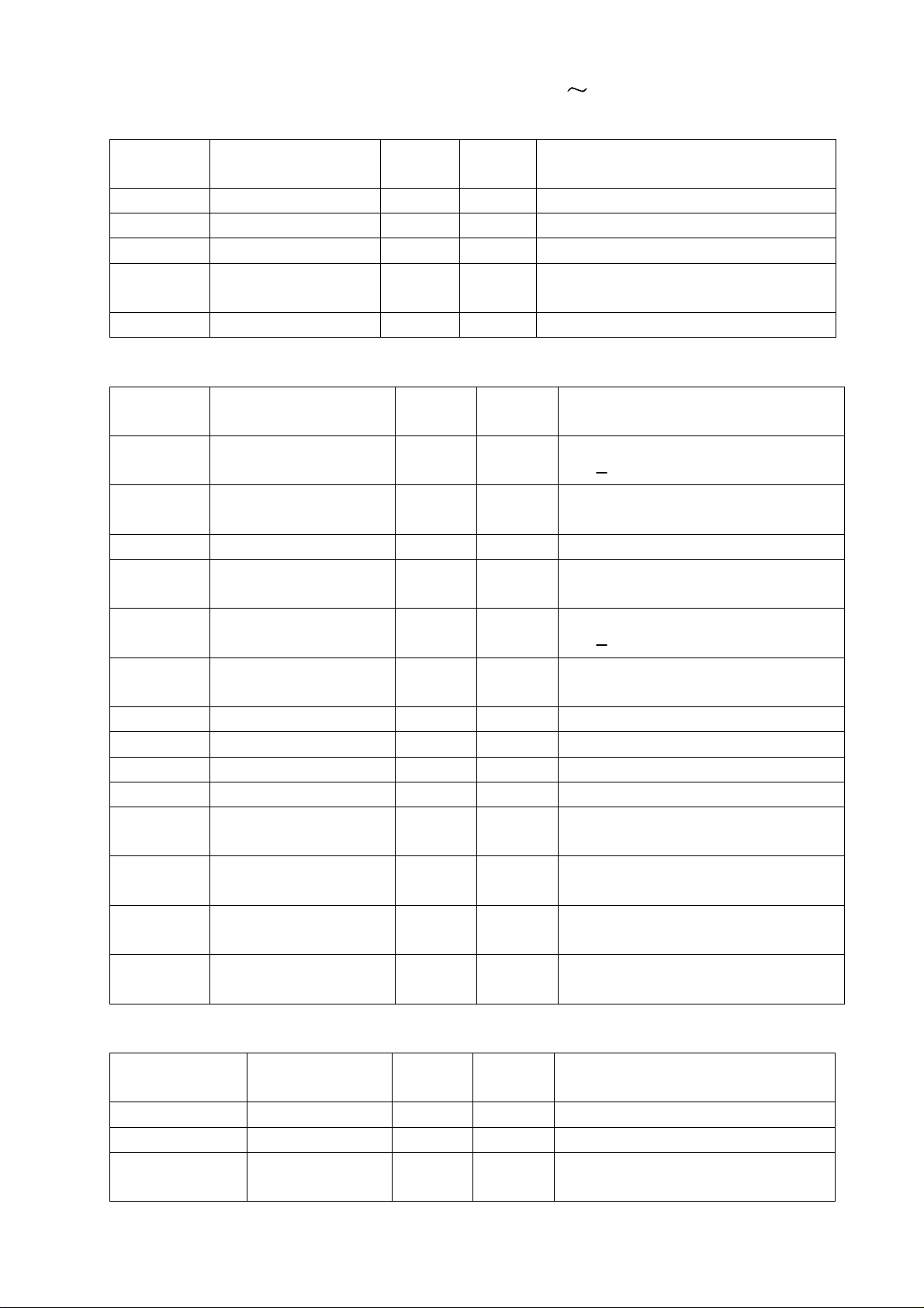
Chart 1 High voltage requirement
T2751
T3251
Model
High voltage normal
value
30 kV
30 kV
1 kV
1 kV
Utmost value Beam current
35 kV 1.6 mA
35 kV 1.6 mA
Each time a receiver requires servicing, the high voltage should be checked following the HIGH
2
VOLTAGE CHECK procedure in this manual. It is recommended the reading of the high voltage
be recorded as a part of service record. It is important to use an accurate and reliable high voltage
meter.
* When checking, main power (B+) should be kept at 135 V (for Toshiba pure flat CRT).
The primary source of X-RAY RADIATION in this TV receiver is the picture tube. For continuous
3
X-RAY RADIATION protection, the replacement tube must be exactly the same type tube as
specified in the parts list.
Some parts in this receiver have special safety-related characteristics for X-RAY RADIATION
4
protection. For continuous safety, parts replacement should be undertaken only after referring to
the PRODUCT SAFETY NOTICE below.
1.2 SAFETY PRECAUTION
WARNING:
Service should not be attempted by anyone unfamiliar with the necessary precaution on this receiver.
The following are the necessary precautions to be observed before servicing this chassis.
1) Since the power supply circuit of this receiver is directly connected to the AC power line, an
isolation transformer should be used during any dynamic service to avoid possible shock hazard.
2) Always discharge the picture tube anode to the CRT conductive coating before handling the
picture tube. The picture tube is highly evacuated and if broken, glass fragments will be violently
expelled. Use shatter proof goggles and keep picture tube away from the unprotected body while
handling.
1
Page 4

3) When replacing a chassis in the cabinet, always be certain that all the protective devices are put
back in place, such as: non-metallic control knobs, insulating covers, shields, isolation
resistor-capacitor network etc.
4) When replacing parts or circuit boards, disconnect the power cord.
5) When replacing a high wattage resistor (oxiode metal film resistor) on the circuit board, keep the
resistor 10mm (1/2in) away from circuit board.
6) Connection wires must be kept away from components with high voltage or high temperature.
7) If any fuse in this TV receiver is blown, replace it with the FUSE specified in the chassis parts list.
1.3 PRODUCT SAFETY NOTICE
Many electrical and mechanical parts in the chassis have special safety-related characteristics.
These characteristics are often passed unnoticed by a visual inspection and the X-RAY RADIATION
protection afforded by them cannot necessarily be obtained by using replacement components rated
for higher wattage, etc. Replacement parts which have these special safety characteristics are
identified in this manual and its supplement electrical components having such features are shaded
on the schematic diagram and the parts list.
Before replacing any of these components, read the parts list in this manual carefully. The use of
substitute replacement parts which do not have the same characteristics as specified in the parts list
may create shock, fire, X-RAY RADIATION or other hazards.
1.4 Testing equipment
HDTV signal generator: VG853 or other same type, 1 set.
Signal generator: PM5515 or the same type, 1 set.
Voltameter: FULK805A or the same type, 1 set.
White balance alignment equipment: 1 set
Standard testing jigs: 1 set.
Geometry alignment equipment: 1 set.
Alignment stick: 1 set.
Degaussor: 1 set.
2 Alignment procedure
2.1 Instruction
a) In this chassis since there are a great amount of data needed to be set, these setting all are stored
2
PROM. To reduce the alignment working, use the aligne d E2PROM as a female parent to
in E
copy and then use them. Or refer to appendix chart and preset E
b) To conduct the alignment, the power supply should be AC120 V,60 Hz. The whole unit should be
preheated for 30 minutes.
c) To conduct with color purity, conver gence, white balance alignment or other alignment relative to
color, the CRT should be degaussed thoroughly.
d) Since this chassis adopts modulization structure, before mounting, every module should be
conducted with alignment.
e
The factory menu’s alignment should use XOCECO RC-T03-0A remote control. Press power
switch to turn on the set, in turn press button “SLP-MUTE-AV-MENU” to enter into factory menu.
2
2
PROM value and then use.
Page 5
Press SLP or 0 button to exit. Press MUTE button to preset before Out-factory.
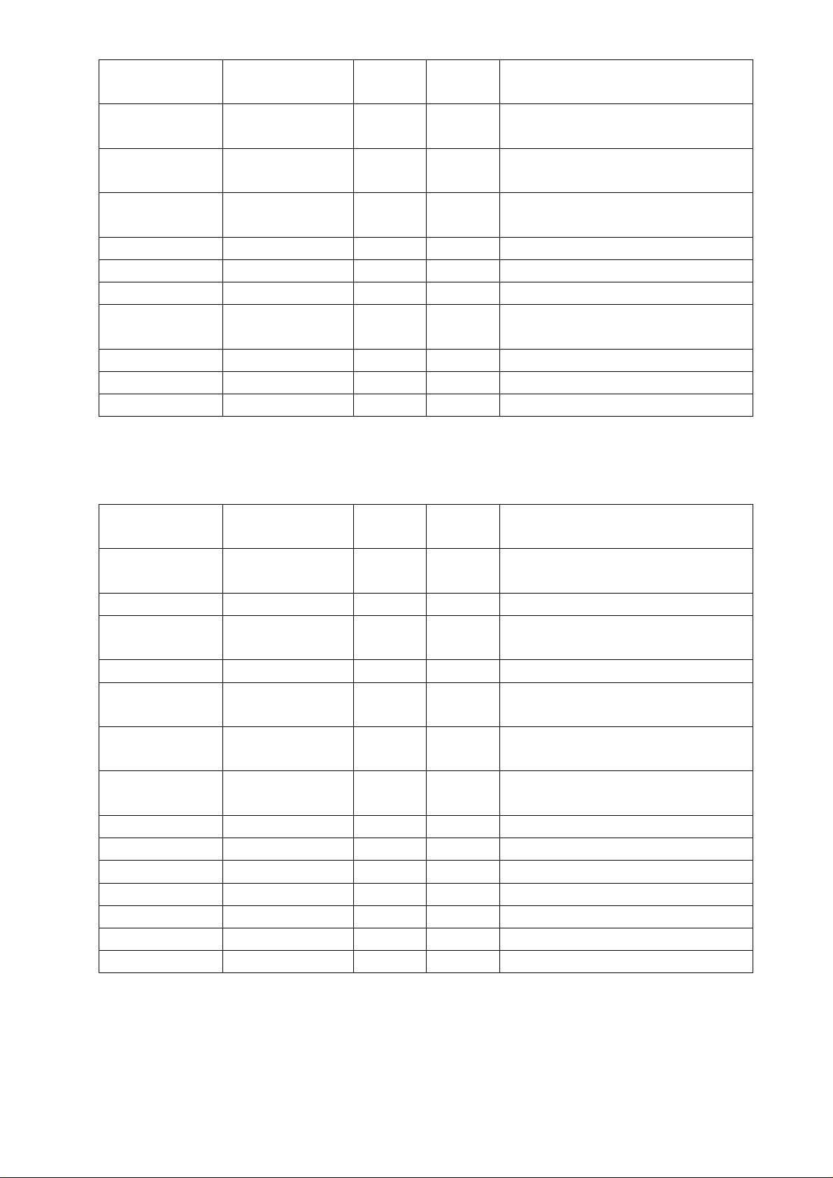
f) For the supporting mode in this set see below chart 2.
Chart 2 The supporting mode in this set
Working mode Mode instruction H-frequency
Hz
TV TV mode 33.75k 60 Adjust firstly, every item should
1920*1080i/33.75K American HDTV mode 33.75k 60 Horizontal and vertical parameter,
720P*576/45.125K American HDTV mode 33.75k 60 Horizontal and vertical parameter,
640*480i(YCrCb) YcbCr(15.7K,59.97HZ) 33.75k 60 Horizontal and vertical parameter,
640*480p(YPrPb) Progressive
DVD(31.5K,60HZ)
33.75k 60 Horizontal and vertical parameter,
V-frequencyHz Alignment instruction
adjust
white balance
white balance
white balance
white balance
2.2 Alignment procedure
2.2.1 Module alignment
In all the module alignment, use a normal working TV set as an alignment frock, pull the set’s
corresponding module and keep it as an example. Insert the module wanted to be check,
then apply power to alignment.
a) AV board module
AV interface function check: check all the AV input/outputs function, it should meet the Product
Standard requirements.
b) Digital processing board module
No alignment point, apply the power and check whether S-VIDEO, YCbCr, YpbPr input is normal.
c) Main board
No alignment point. Apply the power and measure “B+” voltage, the reading should be 105V,
check there are no assemble error, the OSD,SVM is normal, and it is OK.
2.2.2 Chassis adjustment
Correctly insert all modules and parts, connect CRT board parts to CRT, apply power and
check B+ voltage, the reading should be 105V. (on J332/J305)
2.2.3 The whole unit adjustment
Be sure the whole unit has been preheated for 30 minutes.
a) Focus adjustment
1) In TV mode receive crosshatch signal, at the same time set SVM to OFF.
2) Adjust FOCUS inductance L306 on Dynamic Power Board to make R323 dynamic focus
voltage be 1KV+/-50V.
3) Adjust FOCUS potentiometer on FBT and CRT to make horizontal and vertical grid both
thinnest, and consider horizontal grid mainly.
4) Set SVM to ON, check the whole effect.
b) Dark current (SCREEN voltage) adjustment
In TV mode receive gray scale signal, after entering into factory menu status, press “1” button to
enter into “FACTORY MENU 1” factory menu, first preset WHITE-R, WHITE-G, WHITE-B’s
value all to 0, adjust SCREEN potentiometer to make SCREEN LOCK on the screen lower part
3
Page 6
display OK and it is OK, at this time, if changing channel, it should not appear flyback line. This
state should also be OK after finish adjusting the white balance. .
c) White balance adjustment
Adjust on the basis of the above step, at standard status use gray scale signal to adjust.
1
Press “1”button to firstly adjust TV input white balance: fix the testing point at about 40 nits gray
scale, then by adjusting WHITE-R,WHITE-G and WHITE-B to make the value meet chart 3’s
requirement.
2
Press “5” button to adjust YpbPr input white balance: use oscilloscope to measure Y signal
output on Digital Processing Board. Adjust G-0 gray scale to make blanking level be even with
black level, adjust G-G to make signal amplitude to be 0.7V and eight level gray scale be even,
then adjust R-G, B-G, R-0, B-0’s value to make white balance meet chart 3’s requirement.
Chart 3: chroma coordinates requirements
Colour temperature 12000K
X coordinate
Y coordinate
0.270
0.283
0.008 MPDC
0.008 MPDC
d) Picture size position and high voltage adjustment
In component mode input 1080I signal
Use crosshatch and electrical circle signal, after entering into factory menu status, press “2”
button to enter into “FACTORY MENU 2” factory menu to adjust picture’s linearity. Adjust
R339 joint point to make the V-center deflection range be within ±5MM(T3251), or
±3MM(T2751).
Change the signal to white background, or gre atly change contrast and brightness, or press
PIC button to switch among several kinds of analogue amount to make corresponding beam
current changes, adjust V-EHT-COM, H-EHT-COM to make raster’s size basicly not change
when at different beam current status.
3) According to chart 2 in turn apply every testing signal (firstly apply YpbPr signal, then TV or AV
signal), then press “5” button to enter into “FACT ORY MENU 5”, adjust H-S, V-S, H-SIZE, V-SIZE to
make picture normal.
e) Sub-brightness adjustment
Receive split field signal, set colour/contrast/brightness to 0, check whether screen second gray is
slightly bright, otherwise press “6” button, in factory menu select CONTRAST MAX and BRIGHT
MAX to adjust.
f) Filament/beam current/high voltage check and adjustment
1) Filament voltage: receive a TV program signal, set picture mode to “STANDARD”,th e filament
voltage effective value should be 6.3
0.2 Vrms.
2) Beam current check: receive all white field signal, set picture mode to “SPORTS”, measure
R360 two terminals’ voltage and the reading should be less than or be equal to 1.6V. If not,
after entering into factory menu status, press “4” button to enter into “RGB MENU” factory
menu, adjust AV BEAM LIMIT item to make beam current meet requirements.
3) High voltage check: receive D8 signal, set picture mode to “STANDARD”, measure CRT high
voltage and the reading should be A value in chart 3. When brightness, contrast is set to
minimum (zero beam current), measure the high voltage, the reading should not exceed B
value in chart 4.
4
Page 7

Chart 4 High voltage check requirements
Parameters
A
B
74 cm
30 kV
34+ kV
0.5 kV
2751
CRT Size
86 cm
30 kV 0.5 kV
34 kV
3251
4) High voltage protection: receive a picture signal, adjust until picture and sound are normal,
short R340 and the circuit should immediately enter into power-off protection state and the
state should keep. Turn off the power switch and then turn on, the picture and sound should
restore to before-testing state.
g) Peak value adjustment
On the condition of SCREEN and beam current has been adjusted properly, in order to show
picture’s contrast well and control picture’s colour tail, apply a little beam current picture (for
example, black and white crosshatch) and set picture’s contrast and brightness to maximum, then
after entering into factory menu status, press “4” button to enter into “RGB MENU” factory menu,
by adjusting PEAK DRIVE LIMIT item to make the whole unit’s picture colour just without colour tail
on the condition of maximum contrast and it is OK.
h) Every control buttons’ check
Check according to Instruction manual.
i) Check all the input/output terminals’ function, please check according to “PRODUCTION
STANDARD”
i) Out-factory setting
Set picture to “Standard”.
Set sound to “Music”.
Set Blue back to ON.
Set OSD language to English.
Set DNR to SOFT.
Set SVM to ON.
Set Volume to 30.
Set Loudness to OFF.
Set AVC to ON.
Set CCD to OFF.
Set child lock password, V-chip password to 0000.
Set V-chip all rating to no rating .
Set the channel to Cable 3. .
5
Page 8
3 For factory menu adjustment see Chart 5 Chart 11.
Chart 5 Factory menu (1)WRITE
Item name Item instruction Range
WRITE R Bright balance R BF-3F Refer to white balance adjustment part 1
WRITE G Bright balance G BF-3F Refer to white balance adjustment part 1
WRITE B Bright balance B BF-3F Refer to white balance adjustment part 1
SCREEN
LOCK
2003-XX-XX Version date fix
Dark current
adjustment
OK/OFF OK
Default
value
Adjust SCREEN potentiometer until OK
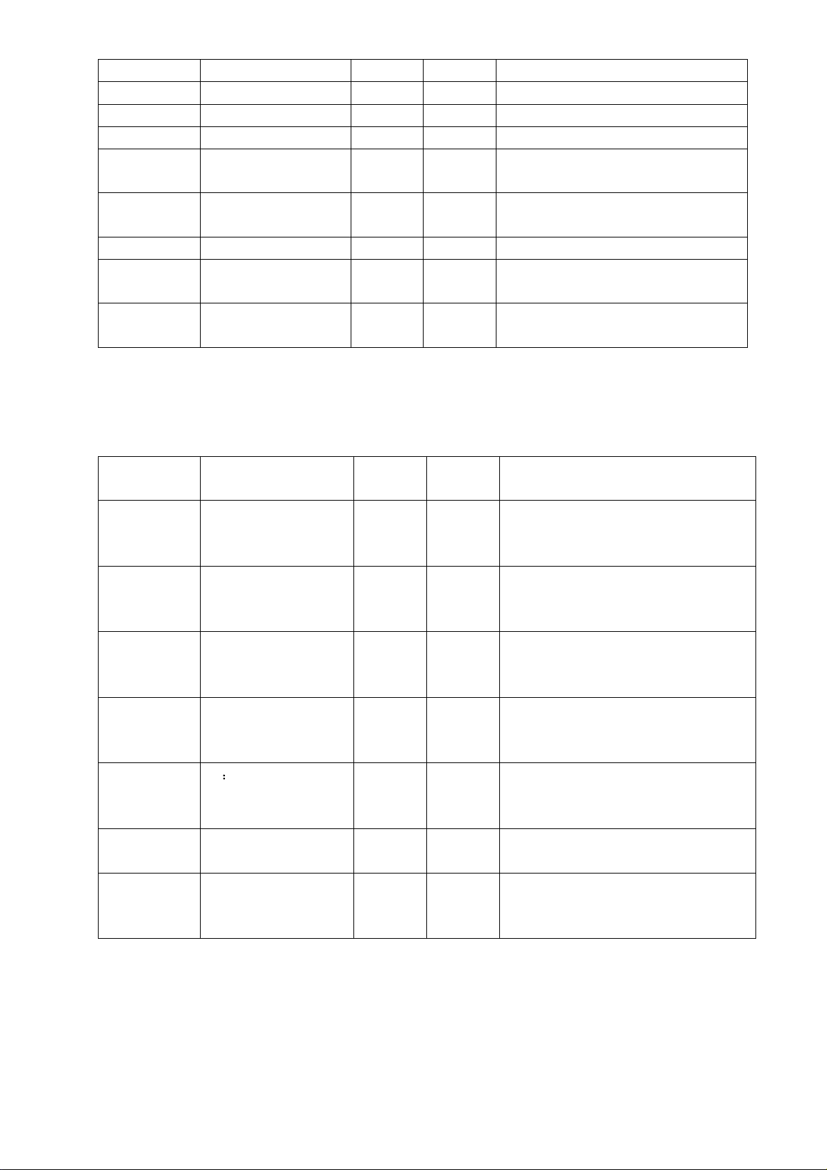
Chart 6 factory menu (2)
Item Item instruction Range
V SIZE V-size 80-7F 39 To make vertical reproduction rate reach
V SHIFT V-center 80-7F 17 To make picture center and CRT center be
V LINEAR V-linearity 80-7F 41 To make V-linearity distortion minimum.
V S CORR Vertical S-correction 80-7F F7 To make vertical S-correction distortion
H SIZE H-size 80-7F 08 To make horizontal reproduction rate reach
H SHIFT H-center 80-7F 43 To make picture horizontal center be in
V ANGLE Parallelogram correction 80-7F 05 To correct parallelogram distortion
V BOW Arch correction 80-7F 0E To correct arch distortion
PIN AMP Pincushion correction 80-7F 60 To make pincushion distortion minimum
PIN PHASE Trapezoid correction 80-7F AE To make trapezoid distortion minimum
UP
CORNER
LOWER
CORNER
EXT
CORNER
V SYNC
CONT
Upper edge corner
correction
Lower edge corner
correction
Edge and corner
correction
80-7F 20
80-7F 11 To correct upper two corners distortion
80-7F C5 To correct lower tow corners distortion
80-7F C5 Corner edge correction
Default
value
90% 92%
in accordance
minimum.
90% 92%
accordance with CRT center.
Chart 7: factory menu (3)
Item Item instruction Range
V SCROLL Vertical scroll 0-FF 00 Not adjust, set default value
V ASPECT V-size 0-FF 00 Not adjust, set default value
V EHT Vertical high
voltage correction
80-7F BD To make vertical raster size not change
Default
value
when beam current changes greatly.
Adjusting method
Adjustment method
Adjustment method
6
Page 9
H EHT Horizontal high
voltage correction
AFC EHT COM High voltage auto
frequency control
H BLANK TIME Horizontal
blanking width
H BLANK PHASE Horizontal
blanking phase
V BLANK START V-sync phase 80-7F FB Not adjust, set default value
V BLANK END V-sync phase 80-7F 11 Not adjust, set default value
MIN NO.OF LINE H-blanking phase 80-1F 00 Not adjust, set default value
MAX NO.OF LINE H-blanking end
position
PWM CONTROL H-blanking width 80-7F 02 Not adjust, set default value
PLL CONTROL 0 H-blanking width 80-7F 0B Not adjust, set default value
PLL CONTROL 1 H-blanking width 80-7F 62 Not adjust, set default value
80-7F 9D To make horizontal raster size not change
when beam current changes greatly.
20-1F 08 Not adjust, set default value
80-7F E4 Not adjust, set default value
80-7F F9 Not adjust, set default value
80-7F FF Not adjust, set default value
Chart 8 Factory menu (4)RGB MENU
Item Item instruction Range
INT H-SYNC
PHASE
AV BEAM LIMIT Beam current limit 80-7F 1A Refer to beam current adjustment part
AV BEAM LIMIT
CHA
PEA DRIVE LIMIT Peak value limit 80-7F 00 Refer to peak value adjustment part
PEAK DRIVE TOP Top peak value
PEA DRIVE
BOTTOM
PEA DRIVE L-R Left/right edge
DEFLECT 0 80-7F 03 Can not adjust, set default value
DEFLECT 1 80-7F 05 Not adjust, set default value
RGB CONTROL 0 80-7F 84 Not adjust, set default value
RGB CONTROL 1 80-7F 18 Not adjust, set default value
RGB CONTROL 2 80-7F 20 Not adjust, set default value
RGB CONTROL 3 80-7F 03 Not adjust, set default value
V INPUT MODE 80-7F 85 Not adjust, set default value
H-sync phase 80-7F 12 Not adjust, set default value
Beam current limit 80-7F 81 Refer to beam current adjustment part
80-7F 10 Not adjust, set default value
limit
Bottom peak
value limit
peak value limit
80-7F 47 Not adjust, set default value
80-7F 88 Not adjust, set default value
Default
value
Adjustment method
7
Page 10
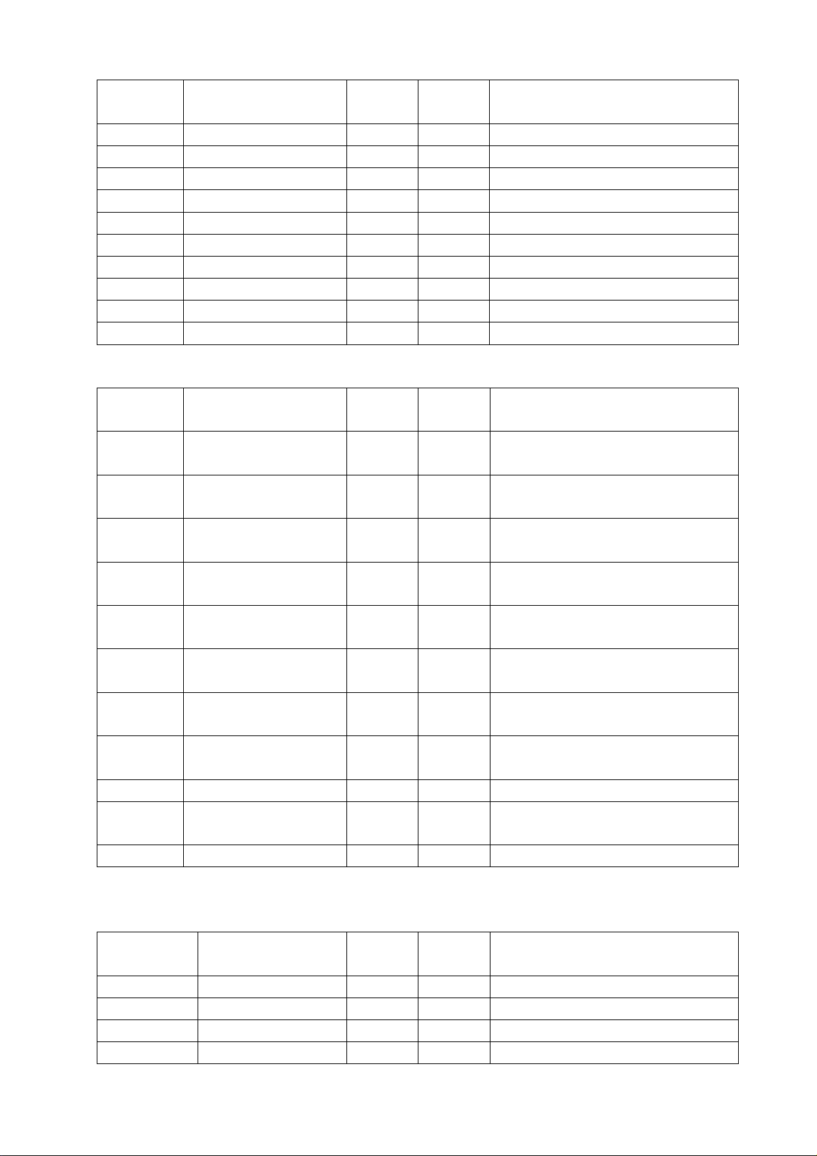
Chart 8 factory menu FACTORY 5(HDTV mode)
Item Item insturction Range
R-G Red gun gain 00-FF 80 Refer to white balance adjustment part2
G-G Green gun gain 00-FF 80 Refer to white balance adjustment part2
B-G Blue gun gain 00-FF 80 Refer to white balance adjustment part2
R-O Red gun bias value 00-FF 80 Refer to white balance adjustment part2
G-O Green gun bias value 00-FF 80 Refer to white balance adjustment part2
B-O Blue gun bias value 00-FF 80 Refer to white balance adjustment part2
H-S H-phase 00-FF Geometrical adjustment
V-S V-phase 00-FF Geometrical adjustment
H-SIZE H-size 00-FF Geometrical adjustment
V-SIZE V-size 00-FF Geometrical adjustment
Default
value
Adjustment method
Chart 9: factory menu 6
Item Item instruction Range
CONTRAST
MAX
CONTRAST
CEN
CONTRAST
MIN
BRIGHT
MAX
BRIGHT
CEN
BRIGHT
MIN
COLOR
MAX
COLOR
CEN
COLOR MIN Colour minimum value 00-7F 00 Not adjust, set to default value
SHARP
MAX
TINT CEN Tint center value 00-7F 00 Not adjust, set to default value
Contrast maximum 00-7F 7F Not adjust, set to default value
Contrast center value 00-7F 3F Not adjust, set to default value
Contrast minimum value 00-7F 00 Not adjust, set to default value
Brightness maximum value 00-7F 7F Not adjust, set to default value
Brightness center value 00-7F 3F Not adjust, set to default value
Brightness minimum value 00-7F 00 Not adjust, set to default value
Colour maximum value 00-7F 3F Not adjust, set to default value
Colour center value 00-7F 20 Not adjust, set to default value
Sharpness maximum
value
00-7F 7F Not adjust, set to default value
Default
value
Adjustment method
Chart 10 Factory menu 7
Item Item instruction Range
VOLUME-1 Sound curve 00-7F 0F Not adjust, set to default value
VOLUME-25 Sound curve 00-7F 1F Not adjust, set to default value
VOLUME-50 Sound curve 00-7F 3F Not adjust, set to default value
VOLUME-100 Sound curve 00-7F 7F Not adjust, set to default value
Default
value
Adjustment value
8
Page 11
BASS MAX Bass maximum value 00-7F 7F Not adjust, set to default value
BASS MIN Bass minimum value 00-7F 00 Not adjust, set to default value
TREBLE MAX Treble maximum value 00-7F 7F Not adjust, set to default value
TREBLE MIN Treble minimum value 00-7F 00 Not adjust, set to default value
SURROUND
MAX
SURROUND
MIN
BLANCE CEN Balance center value 00-7F 20 Not adjust, set to default value
LOUDNESS
ON
LOUDNESS
OFF
Surround sound
maximum value
Surround sound
minimum value
Setting value when
loudness is on
Setting value when
loudness is off
00-7F 7F Not adjust, set to default value
00-7F 00 Not adjust, set to default value
00-7F 7F Not adjust, set to default value
00-7F 00 Not adjust, set to default value
Chart 11 Factory menu 8
Item Item insruction Range
OSD-HP
MENU
OSD-HP AV
SEL
OSD-HP
NORMAL
SVM DELAY SVM delay phase 00-7F 03 Not adjust, set to default value (after
ZOOM DATA
OPTION
DATA1
H-MUTE
DELAY
MENU phase 00-7F 00 Not adjust, set to default value (after
AV menu phase 00-7F 00 Not adjust, set to default value(after
Other menu phase 00-7F 00 Not adjust, set to default value (after
9 picture zoom
16
OPTION 00-FF 01 Not adjust, set to default value
Horizontal failure of
oscillations time delay
amount
80-7F 20 Not adjust, set to default value(after
00-FF 5A Not adjust, set to default value. If less than
Default
value
adjustment, open the menu again and it
is effective)
adjustment, open the AV selection menu
again and it is effective)
adjustment, open the OSD again and it is
effective)
adjustment, turn on the set again and it is
effective)
adjustment, turn on the set again and it is
effective)
10, the screen will light and burn the tube.
Adjustment method
9
Page 12

Chart 12 Factory menu 9 DESIGN MENU
Item Item instruction Range
IC XXX Relative IC chip
ADD H Address high 8 byte 00-FF Press VOL+/- button to change
ADD L Address high 8 byte 00-FF Press VOL+/- button to change
DATA H Data high 8 byte 00-FF Press VOL+/- button to change
DATA L Data lower 8 byte 00-FF Press VOL+/- button to change
READ Reading current data YES/NO
REFRESH Reflesh changed data YES/NO
SAVE Save changed data YES/NO
Default
value
Adjustment method
10
Page 13
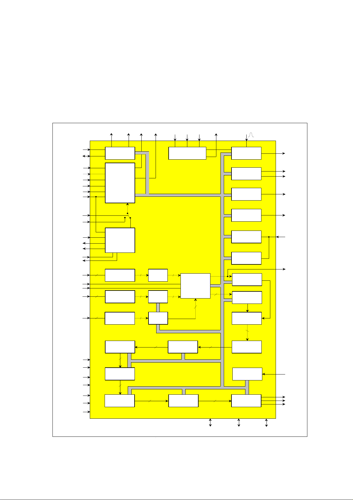
4.General description of the SDA 9380-B21.
The SDA 9380 is a highly integrated deflection controller and RGB video processor for CTV
receivers with 15 to 19kHz or 31 to 38kHz line frequencies. The deflection component controls
among others a horizontal driver circuit for a flyback line output stage, a DC coupled vertical
saw-tooth output stage and an East-West raster correction circuit. All adjustable output
parameters are I2C-Bus con-trolled. Inputs are HSYNC and VSYNC. The HSYNC signal is the
reference for the internal clock system which includes the ¦µ1 and ¦µ2 control loops.
Block diagram of the SDA 9380-B21:
SCL
SDA
BSOIN
RESN
TEST
FH1_2
VSYNC
HSYNC
CLEXT
CLKI
HSAFE
H35K
H38K
RGB 2
FBL 2
FBL 1
RGB
/
YUV
YUV/RGB
X1
X2
SWITCH D/A
I²C
CONTROL
VBLO
SCP
HPROT
VPROTSSD
PROTECTION
START UP
PROTON
H-OUT
V-OUT
EW-OUT
HD
VD+
VD-
E/W
CLL
PWM
PLL
CLAMP
3
1
0
CLAMP
3
CLAMP
3
MATRIX
3
MATRIX
3
MATRIX
3
YUV
3
SWITCH
YUV
3
YUV
Y
UV
2
3
PW/PH- CORR
AVERAGE
BEAM LIMITER
BLACK
STRETCH
SATURATION
CONTROL
UV
RGB
MATRIX
Y
PWM
IBEAM
SVM
VDD(A1..4)
VSS(A1..4)
VDD(D1..2)
VSS(D1..2)
VDD(MC)
VSS(MC)
SUBST
BRIGHTNESS
CONTROL
3
DELAY
3
BLUE STRETCH
3
CONTRAST
CONTROL
3
PEAK DRIVE
3
LIMITER
3
3
VREFC
MEASURE
PULSES
CUT OFF +
WHITE POINT
OUTPUT
BUFFER
VREFH
VREFN
DCI
ROUT
GOUT
BOUT
11
Page 14

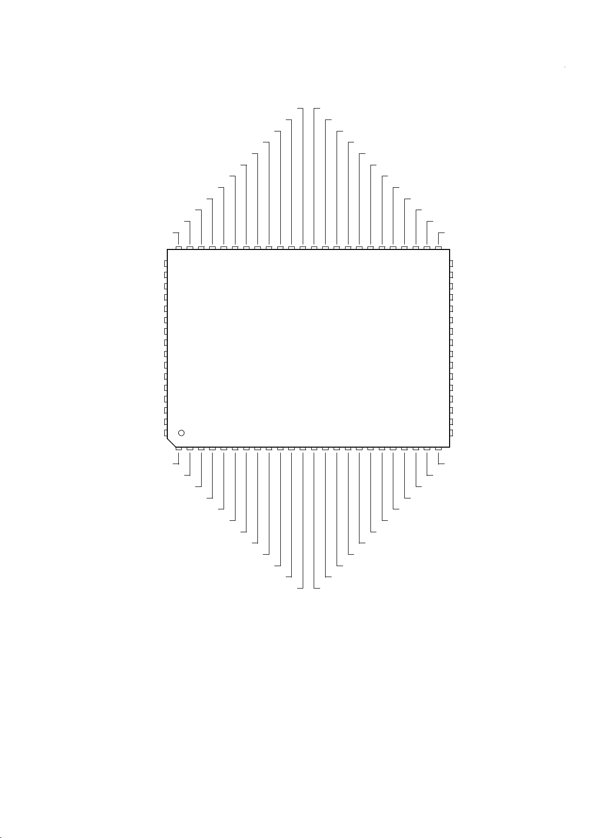
PIN CONFIGURATION:
CLKI
X2
X1
CLEXT
TEST
SUBST
RESN
SCL
SDA
VDD(D)
VSS(D)
HD
H35K
H38K
PWM
VSS(D)
VDD(D)
SSD
SWITCH
64 63 62 61 60 59 58 57 56 55 54 53 5152 50 49
1
SVM
BOUT
SCP
VSS(MC)
VDD(MC)
ROUT
GOUT
R2
G2
B2
2
3
4
5
6
7
8
9
SDA 9380
10
11
12
13
14
15
16
17 18 19 20 21 22 23 24 25 26 27 28 3029 31 32
D/A
FH1_2
=
HSYNC
VSS(A1)
VDD(A1)
E/W
VSS(A2)
VDD(A2)
VD-
VD+
VPROT
VSS(A3)
VDD(A3)
FBL2
FBL1
48
47
46
45
44
43
42
41
40
39
38
37
36
35
34
33
HSAFE
HPROT
B/V 1
G/U 1
R/Y 1
VSS(A4)
V/B 0
U/G 0
Y/R 0
VDD(A4)
DCI
VREFC
VREFN
VBLO
VREFH
PROTON
IBEAM
BSOINVSYNC
12
Page 15

5.Introdution of the VPC 3230D.
The VPC 3230D is a high-quality, single-chip video front-end, which is targeted
for 4:3 and 16:9, 50/ 60 and 100/120 Hz TV sets. It can be combined with other
members of the DIGIT3000 IC family (such as DDP 33x0A/B, TPU 3040) and/or
k
c
T
b
U
Y O
T
C
C r
OE
OU
Y C
6
1
tter
tput
u
O
er
l
S c a
2D
Y
IT U-R 65
F o rma
IT U-R 60
a
de
ram
P IP
Mo
P ano
C r
L
T
F IF O
C N
l
ry
mo
C ontro
Me
s
t
g
s
es
n
ra
tn
t
h
n
a ki
C o
P e
B rig
C b
c
lo
C
L L
S ync
s
C B u
2
I
c
n
n
y
H S
k
O
V S y
AV
ion
+
nerat
C loc
e
G
k
.
n
C loc
G e
s
u
C B
2
I
z
.25 MH
20
r
e
Mix
Y
lor
C o
tiv e
ap
d
A
alog
An
r
e
d
o
c
De
b
C om
nd
e
-
t
on
F r
C r
C b
n
tio
L
P A
NT S C
S E C AM
C
lter
F i
S
NT
C
AG
t
n
T i
tura
S a
Y
C r
C b
F B
s
ing
L
es s
P A
P roc
G
Y /
ADC
×
2
alog
An
t
on
ix
r
ras
t
ont
Ma
C
R
V/
U/B
ent
n
t
nes
n
rati
u
T i
ght
S at
B ri
F B
ADC
on t-E nd
mpo
r
o
F
C
4 x
C IN
VIN1
VIN2
VIN3
it can be used with 3rd-party products.
Block diagram of the VPC 3230D:
T
U
VIN4
V O
B /
R G
Y C rC b
B /
F B
R G
Y C rC b
13
Page 16
PIN CONFIGURATION:
XT AL1
XT AL2
AS G F
64 63 62 61 60 59 58 57 56 55 54 53 52 51 50 49 48 47 46 45 44 43 42 41
65
G NDF
66
VR T
67
I2C S E L
68
IS G ND
69
VS U P F
70
VO UT
71
C IN
72
VI N1
73
VI N2
74
VI N3
75
VI N4
76
VS U P AI
77
G NDA I
78
VR E F
79
F B1 IN
AIS G ND
80
1 2 3 4 5 6 7 8 9 10 1112 13141516 17181920 2122 2324
NC
VS T BY
C LK 5
F PDA T
F S Y/HC
MS Y /HS
VS
IN TL C V S UP S Y
AV O
VP C 323X D
G NDS Y
C 0
C 1
C 2
C 3
G NDC
VS UP C
C 4
C 5
C 6
C 7
40
Y 0
39
Y 1
38
Y 2
37
Y 3
36
VS U P Y
35
G NDY
34
Y 4
33
Y 5
32
Y 6
31
Y 7
30
G NDL LC
29
VS U PL LC
28
LL C1
27
LL C2
26
VS U P PA
25
G NDP A
B 1/CB 1IN
G 1/Y1IN
R 1/CR 1 IN
B 2/CB 2IN
G 2/Y2 IN
R 2/CR 2 IN
AS G F
NC
VS UP C AP
VS UP D
G NDD
G NDC AP S CL
C LK 20
F FOE
F FR E
F FR S TW
F FWE
F FIE
Y CO EQ
VG A V
T E ST
R E S Q
S DA
14
Page 17

6.Introdution of the MSP 3425G.
The MSP 3425G family of single-chip Multistandard Sound Processors covers the sound
processing of all analog TV standards worldwide, as well as the NICAM digital sound standards.
The full TV sound processing, starting with analog sound IF signal-in, down to processed analog
AF-out, is performed in a single chip.
Simplified functional block diagram of the MSP 3425G:
r
e
k
S
Loud-
spea
C
DA
er
es sing
ound
Loud-
S
spea k
P roc
e-
es sing
P r
proc
2
I
C
DA
ct
e
ce S el
S our
e
ca l
P res
1
T
AR
S C
t
T
c
R
put
e
t
l
A
u
S e
O
S C
e
l
ca
s
e
P r
PIN CONFIG
or
De-
modulat
C
AD
1
F
ound I
S
S 1
S 2
2
2
I
I
1
T
AR
S C
C
AD
t
T
c
P
e
l
AR
nput
DS
I
S e
S C
2
T
AR
S C
NO
MO
15
Page 18

I2
DAC M
DAC
M
NC
_
L
26
25
VE R F
_
R
24
NC
2
23
22
R E
S E T
NC
Q
21
20
S _
DA_
I
NC
N2
19
18
DV S U P
DV S S
17
16
M
27
28
29
30
31
32
33
34
35
36
37
NC
NC
VR E F
S
S
NC
AH V S
C
AH V S
AG NDC
C
C
1_OU
1_OU
1
T
T
_R
_L
A
P
L_M
UP
S
NC
ADR _
C L
15
S P
38
NC
ADR _
WS
14
34
39
S
C
2_IN
_
L
ADR
_
DA
13
x5G
40
S
C
2_IN
_
R
I2
S _
DA_
I
N1
12
41
S
C
1_IN
_
L
7.General description of the PW1235.
D_C
I2
S _
DA_
I2S
_
O
W
UT
S
11
10
42
43
S
VR E F
C
1_IN
T
O
_
R
P
I2
I2S
C
_
_
DA
C L
9
8
44
45
MO
AV S
N
S
O
_
I
N
S T
ADR _
AN DB Y
I2
C _
C L
7
46
AV S
UP
S
E
Q
L
6
5
47
48
AN A_
AN A_
I
I
N
N
1
D_C
T
T
R _
R _
I/O_ 0
I/O_ 1
NC
TP
4
3
2
1
49
50
51
52
NC
TE
XT
XT
AL
S T
E
N
AL
_
_
IN
O
UT
The PW1235 Video Signal Processor is a high quality, digital video signal processor that
incorporates Pixelworks' patented, state-of-the-art video deinterlacer and scaler. Using
sophisticated algorithms, the PW1235 is able to effectively deinterlace video input by creating
motion vectors that follow frame-to-frame movement, and provide clear, progressive output in
both analog and digital formats.
With support for NTSC and PAL video formats, the PW1235 can be designed into any TV,
monitor, or projector application. Support for 3:2 and 2:2 film mode detection enables the
PW1235 to provide the best quality display for existing film and video standards. The PW1235
can dynamically enter or exit film mode (with flexible programming) to display mixed content
with the best possible quality.
As a single device, the PW1235 integrates many functions onto one chip. It has embedded a
scaler, an advanced deinterlacer, memory controller, color space converter, and Digital-toAnalog Converter (DAC) onto one chip. There are two video input ports-a primary video port
and a secondary input port-that are used to accept YUV video in the ITU-R601 and ITU-R656
formats respectively. Video content is analyzed on a single-pixel granularity to detect
presence or absence of noise and compute the amount of motion. Motion video is processed
using a highly intelligent algorithm that simultaneously eliminates noise and interpolates pixels
along any angle to produce a noise-free picture without jagged-edge artifacts.
As part of a Pixelworks solution, combining the PW1235 with a Pixelworks ImageProcessor
(such as the PW113, PW166 or PW181) offers the world's best combination of
16
Page 19

deinterlacing and scaling of video or graphics. This combination of high quality deinterlacing
and scaling is essential for higher resolution outputs such as XGA, SXGA, and UXGA that
need to display NTSC and PAL video.
Internal block diagram of the PW1235:
Digita l
Output
Ti mi n g
Ti mi n g
Display
Up
Scaler
P-Channel
Deinterlacer
YU V
CSC
(YUV )
Video
Video
Enhancements
RGB
Merge
CSC
CSC
Analog
Output
DACs
HSync
Timi ng
VSync /
Blue
Screen
LUT
Color
Data
Digita l
Output
Dis play Unit
I-Channel
(I/P)
Picture
Detecti on
(3:2 & 2:2)
Film-Mode
Memory Unit
Primary
Video
Previ ou s
I-Channel
P-Channel
B-Channel
Progra mming Unit
Noise
Moti on
Reduction
Input Unit
Detect and
Down
Scaler
PW1235
Input
Video
Internal Block Diagram
601
ITU-R BT
Primary
Video Port
656
ITU-R BT
Secondary
Video Port
24-Bi t
Port
Digital
Grap hi cs
Interface
Tw o -W i re
17
Page 20

PIN CONFIGURATION:
MCU C M D
MCUWR
MCUCS
PV SS
MCURDY
VSS
MCUD7
MCUD6
MCU D 5
MCU D 4
MCU D 3
192
191
190
189
188
187
186
185
18 4
18 3
PVSS
DPAVSS
DP AVD D
DPDVS S
DPDVDD
PVDD
MV E
PVSS
MA4
MA3
VDD
MA5
MA2
PVDD
MA6
MA1
MA7
PVSS
MA0
MA8
MA 10
PVDD
MA9
MA 13
VS S
MA 11
MA 12
PVSS
MCL K F B
PVDD
MRA S
MCA S
MWE
PVSS
MCL K
PVDD
MD8
MD7
PVSS
MD9
VDD
MD6
PVDD
MD10
MD5
PVSS
MD11
MD4
PVDD
MD12
MD3
PVSS
MD13
MD2
PVDD
MD14
VS S
MD1
PVSS
MD15
MD0
PVDD
193
194
NC
195
NC
196
197
198
199
200
201
202
203
204
205
206
207
208
209
210
211
212
213
214
215
216
217
218
219
220
221
222
223
224
225
226
227
228
229
230
231
232
233
234
235
236
237
238
239
240
241
242
243
244
245
246
247
248
249
250
251
252
253
254
255
256
123456789101112131415161718192021222324252627282930313233343536373839404142434445464748495051525354555657585960616263
VB 0
VB 1
VB 2
VB 3
VB4
VDD
18 2
VB5
VB6
VB7
PVS S
MCU D 2
PV DD
MCUD1
MCUD0
MCUA7
MCUA6
VDD
MCUA5
MCU A4
MCU A3
PV SS
MCU A 2
MCUA1
MCUA0
ADGVSS
ADGVDD
PVDD
A DAV SS
ADAVDD
VREF O UT
VREF I N
COMP
RSET
AV S33 R
AV D3 3R
ADR
AVS33G
AVD33G
ADG
AVS 33B
AVD33B
ADB
ADDVDD
ADD V SS
PV SS
CGMS
DEN
TEST CL K
PVDD
DR7
DR 6
VDD
DR5
DR4
PV SS
DR3
DR2
VSS
DR1
DR0
PVDD
DG 7
DG6
181
180
179
178
177
176
175
174
17 3
17 2
171
170
169
168
167
166
165
164
163
16 2
16 1
160
159
158
157
156
155
154
153
15 2
15 1
15 0
149
148
147
146
145
144
143
142
14 1
14 0
139
138
137
136
135
134
133
132
131
13 0
12 9
128
DG5
127
DG4
126
PVSS
125
DG3
124
DG2
123
VDD
122
DG1
121
DG0
120
PVDD
119
DB7
118
DB6
117
DB5
116
DB4
115
PVSS
114
DB3
113
DB2
112
VSS
111
DB1
110
DB0
109
PVDD
108
DENR
107
DENB
106
DENG
105
PVSS
104
DHS
103
DVS
102
DCLK
101
PVDD
100
DGR7
99
DGR6
98
DGR5
97
DGR4
96
PW1235
TDI
VSS
VG 0
VG1
VG2
VG3
VSS
VG4
VG5
VG6
SV HS
SV VS
PVD D
SV CLK
VG7
PV SS
VR0
VR1
VR2
VR3
VR4
VR5
VR6
VR7
CREF
PVVS
PVHS
PVDD
PV CLK
VDD
PVSS
XTALI
PVDD
2WA1
2WA2
XTALO
TCK
TDO
TMS
PV SS
2WCLK
2WDAT
TEST
PV SS
PVDD
TRSTN
RESETn
MPDV SS
MPAVSS
MPDVDD
MPAVDD
PVSS
95
DGR3
94
DGR2
93
VDD
92
DGR1
91
DGR0
90
PVDD
89
DGG7
88
DGG6
87
DGG5
86
DGG4
85
PVSS
84
DGG3
83
DGG2
82
DGG1
81
DGG0
80
PVDD
79
DGB7
78
DGB6
77
VSS
76
DGB5
75
DGB4
74
PVSS
73
DGB3
72
DGB2
71
DGB1
70
DGB0
69
PVDD
68
DGCLK
67
DGVS
66
DGHS
65
PVSS
64
NC
NC
PVDD
18
Page 21

8.General description of the TDA6111Q.
The TDA6111Q is a video output amplifier with 16 MHz bandwidth. The device is contained
in a single in-line 9-pin medium power (DBS9MPF) package, using high-voltage DMOS
technology, intended to drive the cathode of a colour CRT.
Block diagram of the TDA6111Q:
PIN CONFIGURATION:
rr ent
ent
cath ode
tra ns i
ou tput
u
o utput
C
cath ode
D
bla ck c
meas ur ement
ou tput
7
R OR
MIR
F OL LO WE R S
9
ou tput
feedbac k
tag e
s uppl y v ol
6
HIG H
input
7 V
R OR
MIR
8
bia s
V
par
C
5
R
O
R
MIR
T
E
C
E N
R
R
R
U
S OU
TDA 6111Q
L
TIA
E
G
E N
E R
S TA
IF F
D
C
R
O
R
MIR
8
5
MG A0
input L OW
s uppl y v olta ge
nd
42
grou
(s ubs trate )
h
gew idt
ndb ook , fu ll pa
ha
3
1
i
input
input
inve rting
no n-inv ert
19
Page 22

P INNING
S YMB OL P IN DE S CR IP TIO N
V
V
V
ip
DDL
in
1 non-inver ting v oltage input
2 s upply voltage L OW
3 inverting v o ltage input
G N D 4 g round, s ubs trate
I
om
5 black c urr ent me a s urement
ou tput
V
V
V
V
DDH
cn
oc
fb
6 s upply voltage H IG H
7 cathode trans ient volta ge ou tput
8 cathode DC voltage o utput
9 feedbac k v oltage outpu t
ndb ook , h alfp age
V
1
ip
V
2
DDL
V
3
in
G ND
4
V
I
om
DDH
V
V
V
cn
oc
TDA 6111Q
5
6
7
8
9
fb
MG A05 7
F ig.2 P in c onfiguratio n.
20
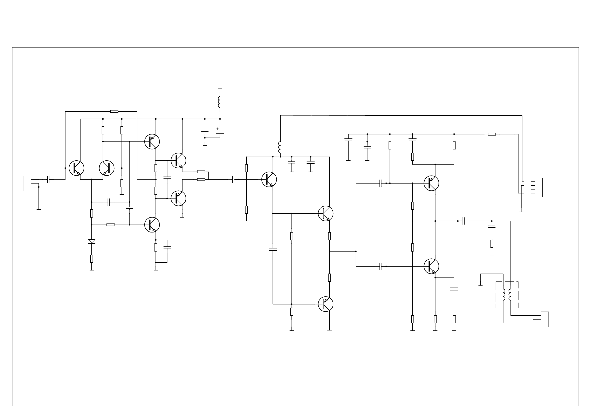
Page 23

Wiring Di agram
491-752J0-02
AC POWER
665-89501-02
SWITCH BOARD
782-13Y90-050A
X1
DEGAUSS COIL
X501
KEY BOARD
782-T3251-0500 782-T32511-2900
665-21201-05
MAIN BOARD
782-T3251-0100
X502 X101 X503
X203 X201 X202
X901
X902 XA01
665-51201-66
665-41201-188
665-81201-40
AV BOARD
FRONT AV BOARD
782-T3251-2900
XAA4 XAA5 XAA6
665-4E301-49
SPEAKER
X401
CRT BOARD
782-T3251-0200
X205
X402 X403
665-64301-06
GND FOCUS
X302
C330
665-3E301-15
X204
VM BOARD
782-T3251-6400
XV03
665-31201-107
VM COIL
XV01 XV02
665-41201-258
Page 24

BLOCK DIAGRAM
22
Page 25

Page 26

AV1IN
AV2IN
AV1OUT
XA01
C
Y
V
R
L
C
Y
V
R
L
V
R
L
AV BOARD
RA63
100
RA69
100
RA74
1n
1n
RA64
100
CA111
1n
CA110
1n
RA72
100
RA59
100
4K7
RA75
4K7
RA67
RA70
100
RA79
4K7
RA78
4K7
LA20
10uH
LA21
10uH
100
CA106
10n
CA88
100u/10V
CA90
100u/10V
CA93
10u/16V
CA94
10u/16V
CA107
10n
CA87
100u/10V
CA89
100u/10V
CA92
10u/16V
CA91
10u/16V
CA97
100u/10V
RA42
5K6
RA43
5K6
RA83
100K
RA82
LA17
10uH
LA18
10uH
LA19
10uH
100K
LA16
10uH
RA76
100K
RA77
100K
CA105
1n
CA152
CA113
1n
1n
RA65
75
RA71
75
RA81
100K
RA80
100K
RA73
100K
RA84
1K
RA85
1K
CA112
1n
RA60
82
75
RA61
75
RA68
CA108
CA109
RA66
82
+9V
LIM
RIM
CI1
10U
VIM
LA15
CA86
LA09
100U
104
VA19
BC843
COM
YOM
+
CA82
104
VA18
BC843
CA72
0.1u
CA74
220u/16V
R2
+9V
10U
LA38
CA143102
RA143
4.7K
RA149
100K
CA138
10U
CA95 1U
SI1
+
YI1
+
VI1
VI1
1
LI1
+
RI1
+
LI1
CI2
SI2
+
YI2
2
YI1
3
RI1
4
CI1
5
6
SI1
7
VI2
8
LI2
9
YI2
10
RI2
11
CI2
12
+
RA58
CA81
1U
48
RTV
V1
220
RA56
1U
470
CA80
47
44
45
46
TV
LTV
COUT1
LV1
Y1
RV1
C1
S2-1
S-1
V2
CXA2089Q
LV2
Y2
RV2
C2
S2-213S-214V315LV316Y317RV318C319S2-320S-321LV422V423RV4
SI2
+
CA69
10u/16V
1N
RA28 100K
RA26
RA31
VCC
S1D
S2D
S1C
S2C
CA67
10u/16V
+
+
4K7
RA30
82
100K
YI3
LI3
16
15
EN
14
13
12
DD
11
10
9
DC
DA06
1N4148
+
VI2
+
RI2
CA63
+
LI2
CA64 1N
+
VO
DCOUT
RO
LO
DA09
DA12
1N4148
DA05
1N4148
1N4148
DA08
1N4148
DA04
1N4148
CA203
104
NA04
1
IN
2
S1A
3
S2A
4
DA
5
S1B
6
S2B
7
DB
8
GND
PI5V330
DA13
1N4148
GND
+
CA68 10u/16V
100
RA27
RA55
470
43
42
YOUT1
NA02
CA66
10u/16V
4K7
RA29
CI3
RI3
DA07
1N4148
TRAP1
CA71
10N
RA41
100
CA701N
104
CA201
DA10
41
RA57
220
82
1N4148
RA40
10U
CA202
CA75
+
100u/10V
CA131
100U
+
104
CA132
R134 15K
37
38
39
CIN1
BIAS
YIN1
LOUT1
VOUT140ROUT1
MUTE
Vcc
VOUT2
ROUT2
YOUT2
LOUT2
COUT2
DC OUT
SDA
SCL
ADR
24
+
+
CA96
CA98
10u/16V
1u/16V
RA395K6
RA130 1K
MONO
TV2
SI3
Y
LA40
VA28
10K
BC847
RA207
75
LA39
10K
DA14
DA15
1N4148
DA11
1N4148
RA201
1N4148
36
35
34
33
32
31
30
29
28
27
26
25
27K
RA161 100
RA162 100
Pb
27K
RA202
CA205
10U
CA204
104
CA73 103
LA41
VA29
10K
BC847
RA208
75
RA44
RA46
1K
VA17
BC847
RA491KRA471KRA48
Pr
27K
27K
RA203
RA206
27K
RA205
LA4210K
VA30
BC847
CA20610U
RA209
75
RA45
1K
470
VA16
VA15
BC843
BC847
CA99
10u/16V
+
CA10010u/16V
+
220
SIF
+5V
SC1R
SC1L
RO
LO
DA03
+9V
1N4148
RIM
LIM
CA159
+
10U
VS1
LA32
22U
47U
CA166
CA165
CA170
10U
104
CA169
104
+
LA23
10U
10U
LA22
CA158
LA29
100U
CA153
1.5P
LO
RO
VO
DCOUT
SDA
SCL
LA13
22
22
100
CA209
CA220
RA204 27K
CA218
CA208 22
CA20710U
10U
RA214
100
NA05
1
2
VA27
BC847
75
RA210
CA210
CA212
CA211
RA213
10u
104
10U
75
3
4
75
5
RA211
6
M52347
7
8
9
RA212
0
+5V
LA43
10uH
100
10U
CA214
CA213
20
0
19
100
18
17
16
15
14
13
12
1110
RA215
CA216
104
HS1
100
RA216
CA217
104
CA215
L0
LA34 10U
CA140
102
100K
15K
RA133
CA141102
RA139
4.7K
RA146
16
VDD
100K
CA134
10U
13
NA07
12
X
X114X2
TC4052BP
15
Y01Y22Y3Y34Y15INH6VEE7GND
CA133
10U
4.7K
RA137
100K
CA139
RA145
102
LA33
10U
NA06
ZA03
52
XOUT
18.432M
51
XIN
50
CA187
TEST
1.5P
49
NC
48
CA177
103
CA176
56P
1.5N
CA174
+
102
CA173
CA163 1U
+
CA164 1U
+
CA161 1U
+
CA162 1U
+
104
470P
CA175
CA172
IF-
47
IF+
46
AVSU
45
AVSS
44
43
VTOP
42
SC1R
41
SC1L
40
SC2R
39
SC2L
38
37
CA171
104
CA160
10U
+
102
36
3.3U
AGND
35
AHV
+
34
CAPM
33
AHVS
32
NC
31
SCLO
30
SCRO
29
REF1
CA168
CA167
28
102
27
MSP3445
L3
10U
LA36
RA141
4.7K
RA147
CA136
10U
10
B9A
X311X0
RA136
8
CA137
10U
4.7K
100K
RA142
RA150
LA37
10U
CA135
10U
4.7K
CA144
RA148
RA140
102
LA35
10U
1
TP
2
3
IO1
4
IO0
5
SLA
6
STB
7
SCL
8
SDA
9
10
11
100K
100K
RA156
RA155
RA154
DA02
DA01
CA142
102
RA158
RA157
10K
100K
VA23
BC847
VA24
BC847
100
100
100
5C2
5C2
RA131
15K
10K
+
CA154
220U
SC1R
RA13215K
RA135
IO1
IO0
SC1L
R3
L2
R0
IO1
IO0
+5V
SCL
SDA
YI3
LI3
RI3
CI3
SI3
M_L
RST
SCL
SIF
TV2
L2
L3
L0
R0
R3
R2
VIM
SDA
MONO
M_R
XA01
1
V/Y
2
GND
3
L
4
R
5
GND
6
C
7
GND
8
S
9
GND
10
R
11
L
V/Y-G-L-R-G-C-G-S-G-R-L
XA05
M_L
1
STB
2
RST
3
SCL
4
SIF
5
TV2
6
GND
7
L
8
L
9
L
10
GND
11
R
12
R
13
R
14
TV1
15
GND
16
SDA
17
VOL
18
MONO
19
M_R
20
12
DVSU
DVSS
REF2
DACR
DACL
GND
RST
13
14
15
16
1.5N
17
470P
220P
47U
+
LA31
+5V
22U
CA183
CA186
CA182
CA181
18
19
20
21
22
23
24
25
26
RA153
RST
100
CA180
103
CA179
CA178
102
102
CA185
M_R
+
1U
CA184
M_L
+
1U
+9V
+5V
Pb
VS1
COM
YOM
HS1
Y
Pr
XA04
1
+9V
2
+5V
3
Pb
4
GND
5
VS1
6
GND
7
C
8
B
9
R
10
VS2
11
HS2
12
GND
13
G
14
FB
15
Y
16
17
HS1
18
Y
19
Pr
20
GND
RA116
75
Y
Cb
RA120
RA11875
75
Cr
XA03
RA117
75
Y
RA11975
Pb
RA121
75
Pr
Page 27

X401
12V
GND
R
G
B
GND
D
SP
TO MAIN
EHT
N401 TDA6110Q
CRT BOARD
C413
22N
R411
750
C409
104
R413
100
D401
1
2
3
4
5
6
7
8
HZ12B1
R414
10K
R409
2K
V401
C1815
C414
22N
R412
750
R410
1.8K
Vip1Vddl2Vin3GND4Iom5Vddh6Vcn7Von8Vfb
C412
C408
100N
C411
100U
C410
100N
N402
Vip1Vddl2Vin3GND4Iom5Vddh6Vcn7Von8Vfb
C416
100N
C407
100N/250V
R407
51K/1W
TDA6110Q
C419
C415
100N/250V
R416
51K/1W
9
560P/500V
9
560P/500V
L404
L405
L403
R418
2.2/2W
1UH
1UH
1UH
R421
2.2/2W
R417 560/C
R419 560/C
R408 560/C
SG401 300V
R
G
B
SG404 300V
SG402 300V
CRT
H1 H2 G1G2 G4
SG404 2KV
103/2KV
G3
C421
CRT SCREEN
R420
2.2M
L407
22UH
VR401
20M
L409
22UH
Focus
G2
L408
22UH
X403
X402
TO MAIN
200V
6.3V
R415
1.8K
C418
100U
100N
C417
TO CRT GRAND
CAUTION:
All the parts in the sc hmatic diagram marke d
N403 TDA6120Q
Vip1Vddl2Vin3GND4Iom5Vddh6Vcn7Von8Vfb
9
L402
22UH
6
5
4
3
2
1
L406
0.27UH
C420
33UF/250V
L401
10UH
C401
22N
R401
750
R403
1.8K
R405
1K
C404
100U
C402
100N
C403
100N
C405
R404
51K/1W
C406
100N/250V
560P/500V
with the sign of
are extremely important
for safety.
The schmatic diagram is repre se ntative only .
The value of the parts will be changed w ith the
improvement of the c ircuit.
1. The unit of resistance is ohm.
K=1,000 ohm M=1,000,000 ohm
2. The unit of induc tance is H.
mH=1/1,000H uH=1/1,000mH
3. The unit of capacitance is F.
uF=1/1,000,000F pF=1/1,000,000uF
4. The meaning of the sy mbols is below:
small signal ground
large signal ground
Page 28
RV10
1K5
LV01
100uH
12V
XV02
SVM
1
2
3
GND
CV01
100P
VV01
2SC1959
GND
RV06
1K
DV01
IN4148
RV12
68
RV05
8K2
VV02
2SC1959
CV04
220P
RV08
4K7
GND
RV07
10K
RV11
10K
CV06
10N
VV05
2SA562
RV04
180
RV09
180
VV03
2SC1959
RV1368CV25
GND
CV05
10N
47N
GND
VV04
2SC1959
VV16
2SA562
RV02
47
RV03
47
GND
CV03
100N
CV02
100U
CV21
100P
RV35
3.9K
RV34
12K
LV02
100uH
+
VV06
2SC1959
CV22
100u/16v
CV24
RV33
300
RV36
820
0.1u
CV3
+
CV23
100u/16V
VV17
2SC1959
RV31
10
RV32
10
VV18
2SA562
+
CV07
22u/100V
CV08
100n
CV09
1n
CV12
1n
RV16
270
+
47u/16V
RV15
2.2
RV17
15K
RV18
15K
RV21
270
CV10
VV07
2SA1964
2SC5248
RV20
10
VV08
RV01
330/1W
RV14
10
XV01
1
12V
2
GND
3
4
105V
TO CRT BOARD X404
CV13
22n
+
CV11
47u/16v
RV19
2.2
222
RV22
120
CV14
TV01
1
2
3
XV03
VM BOARD
VM-OUT
Page 29

Page 30

XAA3
XAA2
L
R
CY
XAA1
XAA6
123
16789
4
XAA5
10
234
11
123
5
RAA6
560
4
RAA5
560
CAA3
1N
RAA3
82
V
RAA1
100KCAA1
1N
R
LAA2
10UH
L
RAA2
100K
CAA2
1N
LAA1
10UH
1
2
3
4
5
6
7
8
XAA4
U/Y
GND
L
R
GND
C
GND
S
L_O
GND
R_O
GND
L_SP
R_SP
GND
GND
FRONT AV BOARD
RAA4
82
Page 31

CB_VPC
CY_VPC
CR_VPC
CD4
22P
CD5
22P
RST
CD189
CD190
CD192
SCL
SDA
RST
R/Pr
G/Y
B/Pb
DBUSY4
DBUSY5
DBUSY6
DBUSY7
DBUSC4
DBUSC5
DBUSC6
DBUSC7
RD1
2.2M
SCL
SDA
220n
220n
220n
RD18
100
SCL
SDA
R9
75
R10
75
R11
75
RP3
100x4
RP10
100x4
SCL
SDA
CD143
220n
RD39 100
RD40 100
RD38
100
+3.3VD
DBUSY0
DBUSY1
DBUSY2
DBUSY3
LLA0
VS3
HS3
DBUSC0
DBUSC1
DBUSC2
DBUSC3
XD1
10.0MHz
10uF/16V
CD144
1n5
CD155
0.1UF
RP4
100x4
RP5
100x4
RD2
RD3
CD8
0.IUF
CD146
CD145
+
CD147
SCL3
SDA3
47n
390p
+3.3VD
100
100
3230D_VREF
11
12
13
15
16
17
18
20
21
22
23
25
26
27
28
30
31
32
33
35
36
37
38
40
41
43
44
45
47
48
50
51
52
53
55
56
1
2
3
4
6
7
8
9
RD42
100*
CLK20
UD1A
VB0
VB1
VB2
VB3
VB4
VB5
VB6
VB7
SVHS
SVVS
SVCLK
VG0
VG1
VG2
VG3
VG4
VG5
VG6
VG7
PVCLK
CREF
PVVS
PVHS
VR0
VR1
VR2
VR3
VR4
VR5
VR6
VR7
XTALI
XTALO
I2CA1
I2CA2
SCL
SDA
TDO
TCK
TDI
TMS
TRSTn
RESETn
TEST
PW1235
CD130
220n
1
2
3
4
5
6
7
8
9
10
11
12
13
14
15
16
17
18
19
20
21
22
23
24
CD133 1n
Cin
CD134 680n
Yin
CD212 680nG/Y
CD132
CD131
390p
1n5
77
78
80
79
VREF
B1/CB1 IN
G1/Y1 IN
R1/CR1 IN
B2/CB2 IN
G2/Y2 IN
R2/CR2 IN
ASGF
NC
VSUPCAP
VSPD
GNDD
GNDCAP
SCL
SDA
RESQ
TEST
VGAV
YCOEQ
FFIE
FFWE
FFRSTW
FFRE
FFOE
CLK20
CD156
CD162
330p
FB1IN
GNDAI
AISGND
GDNPA25VSUPPA26LLC227LLC128VSUPLLC29GNDLLC30Y731Y632Y533Y434GNDY35VSUPY36Y337Y238Y139Y0
47n
LD13
10uH
CD163
68n
76
75
VSUPAI
UD8
VPC3230D
DBUSY6
DBUSY7
MCUCMD
MCUWR
MCUCS
MCURDY
MCUD7
MCUD6
MCUD5
MCUD4
MCUD3
MCUD2
MCUD1
MCUD0
MCUA7
MCUA6
MCUA5
MCUA4
MCUA3
MCUA2
MCUA1
MCUA0
VREFOUT
VREFIN
COMP
RSET
CGMS
TESTCLK
ADR
ADG
ADB
DEN
DR7
DR6
DR5
DR4
DR3
DR2
DR1
DR0
DG6
DG7
5VA
+2.5VD
CD50
0.1uF
5VA
CD107
0.1uF
CD106
+
10uF
LD4
4.7uH
CD105
0.1uF
CD104
+
10uF
1
4
2
UD6
AMS117
OUT
ADJ/GND
TAB/OUT
IN
3
CD103
0.1uF
CD102
+
10uF
CD127
+
100pF
LD3
4.7uH
5
34
93
123
140
175
205
235
14
29
42
54
69
80
90
101
109
120
131
143
180
208
216
224
230
237
243
249
256
194
197
199
200
58
60
63
64
151
154
157
165
149
163
166
3
CD118
+
10uF
UD1C
VDD
VDD
VDD
VDD
VDD
VDD
VDD
VDD
PVDD
PVDD
PVDD
PVDD
PVDD
PVDD
PVDD
PVDD
PVDD
PVDD
PVDD
PVDD
PVDD
PVDD
PVDD
PVDD
PVDD
PVDD
PVDD
PVDD
PVDD
NC
DPAVDD
DPDVDD
PVDD
MPDVDD
MPAVDD
NC
PVDD
AVD33B
AVD33G
AVD33R
PVDD
ADDVDD
ADAVDD
ADGVDD
PW1235
GVS
GHS
SOG
GHS_PW
+5V1 5VD
CD108
47uF/10V
+5V2
CD109
47uF/10V
UD4
TAB/OUT
IN
ADJ/GND
AMS117
CD97
CD98
+
10uF
LD8
4.7uH
CD120
0.1uF
LD9
4.7uH
LD11
+5V1
AVU3
CD135
390p
VRT
CD148
47n
67
65
66
69
70
71
CIN
VIN172VIN273VIN374VIN4
DBUSY5
VRT
GNDF
VOUT
DBUSY3
DBUSY4
192
191
190
188
186
185
184
183
182
181
179
178
177
176
174
173
172
170
169
168
162
161
160
159
156
153
150
146
145
144
142
141
139
138
136
135
133
132
129
130
ASGF
ISGND68VSUPF
I2CSEL
XTAL2
XTAL1
CLK5
VSTBY
FPDAT
MSY/HS
FSY/HC
INTLC
VSUPSY
GNDSY
GNDC
VSUPC
40
3LLC1
CD164
DBUSY0
DBUSY1
DBUSY2
DBUSY[0..7]
CD2
0.1uF
CD1
0.1uF
RD4
1K
RD6
75
RD5
10K
+3.3VD
CD136
1n5
NC
VS
AVO
C0
C1
C2
C3
C4
C5
C6
C7
68n
RD7
0*
CD137
220n
CD149
+
10uF/16V
64
63
62
61
60
59
58
57
56
55
54
53
52
51
50
49
48
47
46
45
44
43
42
41
RD43
100
+3.3VA
ROUT
GOUT
BOUT
RD8
75
RD9
10K
CD3
+
10uF/16V
RD10
75
CD138
0.1uF
Yin
Cin
RD11
0*
10uH
CD140
+
10uF
CD139
+
10uF
XD2
20.25MHz
CD150
CD151
15p
15p
RD36 100
V1-OUT
H1-OUT
RD37
DBUSC0
DBUSC1
DBUSC2
DBUSC3
DBUSC4
DBUSC5
DBUSC6
DBUSC7
LLA0
R7
75
R8
75
GCLK
GADU[7:0]
AD9883 YUV 4:4:4 INPUT
GADY[7:0]
GADV[7:0]
VS2
HS2
CD152
0.1uF
CD153
0.1uF
100
CD157
1n5
CD158
220n
GHS_PW
GVS
GCLK
RD12
CD141
+
10uF
CD159
1n5
GADU[7:0]
GADY[7:0]
GADV[7:0]
RD13 100
CD154
+
10uF
CD161
47n
CD160
68n
RP1
100x4
GADU0
GADU1
GADU2
GADU3
GADU4
GADU5
GADU6
GADU7
RP6
GADY0
GADY1
GADY2
GADY3
GADY4
GADY5
GADY6
GADY7
RP7 100x4
GADV0
GADV1
GADV2
GADV3
GADV4
GADV5
GADV6
GADV7
RP11
100x4
100
RD14
10K
LD12
10uH
CD142
0.1uF
VS3
HS3
RP2
RD15
10K
+3.3VA
+3.3VD
CD61
0.1uF
CD75
0.1uF
CD51
0.1uF
CD6
22pF
R/Pr
G/Y
B/Pb
+3.3VA
+3.3VD
100x4
100x4
RP8
100x4
RP9
100x4
CD7
22pF
CD62
0.1uF
CD76
0.1uF
CD52
0.1uF
R1
75
R2
75
R6
75
+3.3VA
+3.3VD
CD63
0.1uF
CD77
0.1uF
100
102
103
104
106
107
108
110
111
113
114
116
117
118
119
121
122
124
125
127
128
L1
3.3UH
L2
3.3UH
L3
3.3UH
CD53
0.1uF
66
67
68
70
71
72
73
75
76
78
79
81
82
83
84
86
87
88
89
91
92
94
95
97
98
99
+3.3VA
CD64
0.1uF
+3.3VD
CD78
0.1uF
UD1B
DGHS
DGVS
DGCLK
DGB0
DGB1
DGB2
DGB3
DGB4
DGB5
DGB6
DGB7
DGG0
DGG1
DGG2
DGG3
DGG4
DGG5
DGG6
DGG7
DGR0
DGR1
DGR2
DGR3
DGR4
DGR5
DGR6
DGR7
DCLK
DVS
DHS
DENG
DENB
DENR
DB0
DB1
DB2
DB3
DB4
DB5
DB6
DB7
DG0
DG1
DG2
DG3
DG4
DG5
PW1235
R3
75
R4
75
R5
75
+3.3VA
+3.3VA
+3.3VA
CD65
CD66
CD67
0.1uF
0.1uF
0.1uF
+3.3VD
+3.3Vpll
+3.3Vpll
CD79
CD81
0.1uF
0.1uF
+3.3VD+3.3VD+3.3VD+3.3VD
CD54
CD55
CD56
0.1uF
0.1uF
0.1uF
C1
330p
C2
330p
C3
330p
CD82
0.1uF
CR_VPC
CY_VPC
CB_VPC
+3.3VA
CD68
0.1uF
CD57
0.1uF
JD2
CON15
JD1
CON15
+3.3VA
CD69
0.1uF
+3.3VD+3.3VD+3.3VD+3.3VD
CD58
0.1uF
MD10
MD11
MD12
MD13
MD14
MD15
MCLK
MWE
MCAS
MRAS
MCLKFB
MA10
MA11
MA12
MA13
MUE
MD0
MD1
MD2
MD3
MD4
MD5
MD6
MD7
MD8
MD9
MA0
MA1
MA2
MA3
MA4
MA5
MA6
MA7
MA8
MA9
15
14
13
12
11
10
9
8
7
6
5
4
3
2
1
15
14
13
12
11
10
9
8
7
6
5
4
3
2
1
+3.3VA
CD70
0.1uF
+3.3VD
255
252
248
245
242
239
236
232
231
234
238
241
244
247
250
254
229
227
226
225
223
213
210
207
204
203
206
209
211
214
217
215
220
221
218
201
CD80
0.1uF
+3.3VD
+3.3VD
+2.5VD
MD0
MD1
MD2
MD3
MD4
MD5
MD6
MD7
MD8
MD9
MD10
MD11
MD12
MD13
MD14
MD15
MA0
MA1
MA2
MA3
MA4
MA5
MA6
MA7
MA8
MA9
MA10
MA11
MA12
MA13
RD16
10K
CD9
0.1uF
CD10
0.1uF
CD11
0.1uF
GOUT
BOUT
ROUT
VS2
HS2
+5V2
RST
SCL
SDA
VS_CPU
HS_CPU
+5V1
R/Pr
B/Pb
G/Y
HS_VGA
VS_VGA
Yin
Cin
+3.3VD
CD12
0.1uF
+3.3VD
CD13
0.1uF
+2.5VD
CD14
0.1uF
MD[15:0]
MCLK
MWE
MCAS
MRAS
MCLKFB
MA[13:0]
RD17
0*
+3.3VD
+2.5VD
+3.3VD
R/Pr
G/Y
B/Pb
HS_VGA
VS_VGA
CD15
0.1uF
CD16
0.1uF
CD17
0.1uF
MD[15:0]
MCLKFB
SDA
SCL
CD71 47nF
CD72 47nF
CD73 1nF
CD74 47nF
CD83
0.1uF
+3.3VD
CD18
0.1uF
+3.3VD
CD19
0.1uF
+2.5VD
CD20
0.1uF
MCLK
MWE
MCAS
MRAS
MCLKFB
MA[13:0]
MCLK
+3.3Vpll
RD24
RD25
RD26
RD22
RD23
+3.3VD
CD21
0.1uF
+3.3VD
CD22
0.1uF
+2.5VD
CD23
0.1uF
CD59
3.9nF
680
680
CD84
0.1uF
+3.3VD
+3.3VD
+2.5VD
MA[13:0]
MCLK
MCLKFB
CD60
39nF
100
100
10K
CD24
0.1uF
CD25
0.1uF
CD26
0.1uF
MWE
MCAS
MRAS
+3.3VA +3.3VD +3.3Vpll
59
62
RD21
3.3K
+3.3VD
+3.3VD
+2.5VD
AVD126AVD227AVD339AVD442AVD545AVD646AVD751AVD852AVD9
33
FILT
57
SDA
56
SCL
55
A0
38
CLAMP
29
COAST
RD20
54
48
49
43
30
31
58
37
CD27
0.1uF
CD28
0.1uF
CD29
0.1uF
+3.3VD
+3.3VD
+2.5VD
MWE
MCAS
MRAS
RAIN
GAIN
SOGIN
BAIN
HSYNC
VSYNC
REFBYP
MIDSCV
CD30
0.1uF
CD31
0.1uF
CD32
0.1uF
100
AD9883 KST -110
GND11GND210GND320GND421GND524GND625GND728GND832GND936GND1040GND1141GND1244GND1347GND1450GND1553GND1660GND1761GND1863GND1968GND20
+3.3VD
+3.3VD
+3.3VD
CD33
CD36
0.1uF
0.1uF
+3.3VD
+3.3VD
+3.3VD
CD34
CD37
0.1uF
0.1uF
+2.5VD
+2.5VD
+2.5VA
CD35
CD38
0.1uF
0.1uF
MA0
23
MA1
24
MA2
25
MA3
26
29
MA4
30
MA5
MA6
31
32
MA7
33
MA8
34
MA9
22
MA10
35
MA11
20
MA12
21
MA13
16
17
18
19
15
39
38
37
+3.3VD
UD3
CD39
0.1uF
CD40
0.1uF
CD43
0.1uF
UD2
+3.3VD
+2.5VA
A0
A1
A2
A3
A4
A5
A6
A7
A8
A9
A10
A11
BA0
BA1
WE
CAS
RAS
CS
LDQM
UDQM
CLK
CKE
AVD10
VDD111VDD222VDD323VDD578VDD469VDD6
+3.3VD+3.3VD
+3.3VD
CD41
CD42
0.1uF
0.1uF
CD45
0.1uF
+3.3VD
9
27
VDD1VDD14VDD
VDDQ3VDDQ
HY57V641620HG
VSSQ6VSSQ12VSS28VSS41VSSQ46VSSQ52VSS
79
CD44
0.1uF
VDDQ43VDDQ
35
PVD134PVD2
GREEN0
GREEN1
GREEN2
GREEN3
GREEN4
GREEN5
GREEN6
GREEN7
BLUE0
BLUE1
BLUE2
BLUE3
BLUE4
BLUE5
BLUE6
BLUE7
DATACK
HSOUT
SOGOUT
VSOUT
80
49
DQ0
DQ1
DQ2
DQ3
DQ4
DQ5
DQ6
DQ7
DQ8
DQ9
DQ10
DQ11
DQ12
DQ13
DQ14
DQ15
NC
NC
54
RED0
RED1
RED2
RED3
RED4
RED5
RED6
RED7
2
4
5
7
8
10
11
13
42
44
45
47
48
50
51
53
36
40
77
76
75
74
73
72
71
70
9
8
7
6
5
4
3
2
19
18
17
16
15
14
13
12
67
66
65
64
CD116
10uF
MD0
MD1
MD2
MD3
MD4
MD5
MD6
MD7
MD8
MD9
MD10
MD11
MD12
MD13
MD14
MD15
5VD
5VA
GADV0
GADV1
GADV2
GADV3
GADV4
GADV5
GADV6
GADV7
GADY0
GADY1
GADY2
GADY3
GADY4
GADY5
GADY6
GADY7
GADU0
GADU1
GADU2
GADU3
GADU4
GADU5
GADU6
GADU7
CD95
+
10uF
+
GADV[7:0]
GADY[7:0]
GADU[7:0]
CD96
0.1uF
CD117
0.1uF
MD[15:0]MA[13:0]
+3.3VA
CD46
0.1uF
GCLK
GHS
SOG
GVS
UD5
AMS1085
3
UD7
3
AMS117
MD[15:0]
CD47
0.1uF
GADV[7:0]
GADY[7:0]
GADU[7:0]
Vin
IN
CD48
0.1uF
GCLK
ADJ
1
TAB/OUT
ADJ/GND
LD7
4.7uH
+2.5VD
CD49
0.1uF
+Vout
OUT
+2.5VA
47uF/10V
+2.5VA
+3.3VA
CD126
2
4
2
1
+3.3VD
OUT
+
+
0.1uF
LD2
4.7uH
4
2
1
CD110
100pF
CD111
100pF
CD99
10uF
CD122
10uF
CD123
10uF
RD28
RD35
RD34
RD27 0
LD5
10uH
LD6
10uH
LD10
10uH
+
+
DPAVSS
DPDVSS
MPDVSS
MPAVSS
AVS33G
ADDVSS
ADAVSS
ADGVSS
0
0
0
CD100
+
0.1uF
VSS
VSS
VSS
VSS
VSS
VSS
VSS
VSS
PVSS
PVSS
PVSS
PVSS
PVSS
PVSS
PVSS
PVSS
PVSS
PVSS
PVSS
PVSS
PVSS
PVSS
PVSS
PVSS
PVSS
PVSS
PVSS
PVSS
PVSS
PVSS
PVSS
PVSS
AVS33B
AVS33R
PVSS
CD128
10uF
+2.5VA
+2.5VD
NC
NC
CD112
10uF
CD113
10uF
CD124
0.1uF
CD125
0.1uF
19
49
77
134
187
219
251
112
10
24
39
46
65
74
85
96
105
115
126
137
171
189
202
212
222
228
233
240
246
253
195
196
198
193
59
61
62
57
152
155
158
147
148
164
167
VS_CPU
GHS_PW
GHS_PW
HS_CPU
+
CD101
100pF
+
+
+3.3Vpll
+3.3VD
CD114
100pF
5VA
CD115
100pF
CD129
100pF
Page 32
WARNING: BEFORE SERVICING THIS CHASSIS, READ THE “X-RAY RADIATION
PERCAUTION”, “SAFETY PRECAUTION” AND “PRODUCT SAFETY NOTICE” ON
PAGE 1&2 OF THIS MANUAL.
CAUTION: 1. The shaded areas makes in the schematic diagram and the parts list designate components
which have special characteristics important for safety and should be replaced only with
type identical to those in the original circuit or specified in the parts list. Before replacing
any of these components, read carefully the PRODUCT SAFETY NOTICE on page 2.
2. Do not degrade the safety of the receiver through improper servicing.
ELECTRICAL PARTS LIST
MAIN BOARD
SYMBOL PART NO. DESCRIPTION
782-T3251-0100 MAIN PCB
CRYSTAL
Z101 329-58001-00 8MHZ
Z201 329-62404-00 HC-49/US 24.576MHZ
DISCHARGE TUBE
D322 339-10017-00 DSP-152MS00B
339-10017-00 DSP-152MS00B
DIODE
D102 340-00001-003 1N4148
D103 340-00001-003 1N4148
D510 340-00001-003 1N4148
D502 340-00001-003 1N4148
D202 340-00001-003 1N4148
D503 340-00001-003 1N4148
D301 340-00001-003 1N4148
D504 340-00001-003 1N4148
D505 340-00001-003 1N4148
D305 340-00001-003 1N4148
D312 340-00001-003 1N4148
D507 340-00001-003 1N4148
D315 340-00001-003 1N4148
D314 340-00001-003 1N4148
D101 340-00001-003 1N4148
D320 340-00001-003 1N4148
D323 340-00001-003 1N4148
D104 340-00001-003 1N4148
28
Page 33
SYMBOL PART NO. DESCRIPTION
D523 340-00001-003 1N4148
D318 340-00005-003 S5295J
D511 340-00005-003 S5295J
D319 340-00010-003 S5295G
D313 340-00014-003 RGP10J
D309 340-00086-003 TVR-1B
D311 340-00086-003 TVR-1B
D316 340-00288-003 TFR155
D303 340-00132-00 ERC20-06
D520 340-00197-00 IN4007
D304 340-00254-00 BY459X
D517 340-00257-00 BYT56J
D514 340-00283-00 TRU3YX
D501 340-00288-00 TFR155
D515 340-00288-00 TFR155
D516 340-00288-00 TFR155
REGULATED DIODE
D317 340-50240-003 HZ2C2
D307 340-50390-003 HZ4B2
D512 340-50470-003 HZ5B1
D518 340-50560-003 HZ6B1
D519 340-50560-003 HZ6B1
D522 340-50610-003 HZ6C2
D201 340-50610-003 HZ6C2
D513 340-50610-003 HZ6C2
D306 340-50750-003 HZ7C2
D308 340-51180-003 HZ12A1
D310 340-51850-003 HZ18-3
D509 340-51670-003 HZ16-3
D321 340-51670-003 HZ16-3
D506 340-51850-003 HZ18-3
D508 340-52490-003 HZ24-3
TRANSISTOR
V501 343-04000-304 2SD400 E/F
V207 343-05620-104 2SA562TM-Y
V205 343-05620-104 2SA562TM-Y
V204 343-05620-104 2SA562TM-Y
V202 343-05620-104 2SA562TM-Y
V203 343-05620-104 2SA562TM-Y
V104 343-05620-104 2SA562TM-Y
V001 343-10150-104 2SA1015Y Pr2.5
V206 343-12040-004 RN1204
29
Page 34

SYMBOL PART NO. DESCRIPTION
V507 343-18150-104 2SC1815-Y
V506 343-18150-104 2SC1815-Y
V103 343-18150-104 2SC1815-Y
V504 343-18150-104 2SC1815-Y
V304 343-18150-104 2SC1815-Y
V503 343-18150-104 2SC1815-Y
V201 343-18150-104 2SC1815-Y
V508 343-01800-00 KSE180 TO-126
V509 343-01800-00 KSE180 TO-126
V510 343-01800-00 KSE180 TO-126
V303 343-03040-00 BSN304
V302 343-06880-60 2SB688-0
V301 343-51440-00 2SC5144
V502 343-18150-10 2SC1815-Y
V208 343-07520-10 2SC752GTM-Y
INDUCTANCE WITH COLOUR CODES
L206 471-2A22K-003 SPT0305-2R2K-5
L205 471-2022K-003 SPT0305-220K-5
L208 471-2022K-003 SPT0305-220K-5
L101 471-2022K-003 SPT0305-220K-5
L103 471-2A18K-00 SPT0305-1R8K-5
L207 471-2A47K-00 SPT0305-4R7K-5
L212 471-2010K-A0 SP0203-10uH-K
L503 471-2010K-A0 SP0203-10uH-K
L217 471-2010K-A0 SP0203-10uH-K
L218 471-2010K-A0 SP0203-10uH-K
L307 471-2010K-A0 SP0203-10uH-K
L202 471-2022K-00 SPT0305-220K-5
L209 471-2022K-00 SPT0305-220K-5
L102 471-2068K-A0 SP0203-68uH-K
ADJUSTA BLE INDUCTANCE
L306 477-30027-00 TLN2110
FIXED INDUCTANCE
L304 477-40167-00 PSC1726H-200K5R0 !
L504 477-40031-00 LG750
L301 477-40057-00 LG101
L302 477-40073-00 TLN3197D
L305 477-40179-00 LE1949
RECTIFIER
VD501 340-80011-00 RBV-606
IC
N502 352-06210-70 TLP621-GB(UL) (O)!
30
Page 35

SYMBOL PART NO. DESCRIPTION
N202 352-11170-20 AS1117M-3.3 (M)
N103 352-24160-50 M24C16BN6 (M)
N101 352-37281-10 *M37281EKSP (M)
N301 352-55590-40 TA75559P (D)
N102 352-70390-10 * KIA7039P (D)
N506 352-74950-10 * TDA7495S (D)
N302 352-78041-00 LA78041 (M)
N503 352-78050-00 KA7805 (M)
N505 352-78080-00 AN7808 (D)
N303 352-78090-40 TA78M09P (D)
N504 352-78120-60 KA7812 (M)
N201 352-93800-00 SDA9380-B21 (D)
N501 352-96560-00 STR-G9656 (M)
RELAY
RL501 457-12003-9G JQX-14FF-012-1HS !
CERAMIC CAPACITOR
C502 459-B147M-20 ECK-DNS471MBX !
C501 459-B147M-20 ECK-DNS471MBX !
C520 459-B222M-20 ECK-DNS222MEX !
THIN-FILM CAPACITOR
C504 462-2B410-M0V 250VAC-0.1uF-M !
C503 462-2B410-M0V 250VAC-0.1uF-M !
C506 462-2B410-M0V 250VAC-0.1uF-M !
C512 462-2B410-M0V 250VAC-0.1uF-M !
C310 462-88212-H0 CBB81-1600V-1200PF-J
C307 462-8E247-H4 CBB81-2KV-4700PF-J
C309 462-88224-H0 ECWH12H242JR
ELECTROLYTIC CAPACITOR
C536 464-60822-M0 CD110-16V-2200 uF-M
THERMISTOR
RT502 469-40004-00 5D2-14LC
RT503 469-10028-00 MZ73C-9RM !
METAL RESISTOR
R224 467-2C327-G03 1/6W-27K-G
R308 467-2C327-G03 1/6W-27K-G
R512 467-2C510-G03 1/6W-1M-G
R307 467-2E227-H0 1/2W-2.7K-JL
R323 467-2E227-H0 1/2W-2.7K-JL
R342 467-2E322-H0 1/2W-22K-JL
R329 467-2FA15-H0 1W-1.5Ω-JL
R321 467-2FA56-H0 1W-5.6Ω-JL
R303 467-2FB33-H0 1W-0.33Ω-JL
31
Page 36
SYMBOL PART NO. DESCRIPTION
R328 467-2FB82-H0 1W-0.82Ω-JL
R304 467-2F002-H0 1W-2Ω-JL
R524 467-2F012-H0 1W-12Ω-JL
R330 467-2F110-H0 1W-100Ω-JL
R339 467-2F156-H0 1W-560Ω-JL
R302 467-2F227-H0 1W-2.7KΩ-JL
R322 467-2F315-H0 1W-15kΩ-JL
R513 467-2F333-H0 1W-33kΩ-JL
R505 467-2F368-H0 1W-68kΩ-JL
R509 467-2GB15-H0 2W-0.15Ω-JL
R510 467-2GB15-H0 2W-0.15Ω-JL
R529 467-2F182-H0 1W-820Ω-JL
R310 467-2G224-H0 2W-2.4kΩ-JL
R311 467-2G224-H0 2W-2.4kΩ-JL
R312 467-2G224-H0 2W-2.4kΩ-JL
J517 467-2E139-H0 1/2W-390Ω-JL
MELTABLE RESISTOR
R313 467-4E001-H0 1/2W-1Ω-JL
R535 467-4FB27-H0 1W-0.27Ω-JL
R545 467-4FB27-H0 1W-0.27Ω-JL
R320 467-4FB33-H0 1W-0.33Ω-JL
R523 467-4FB33-H0 1W-0.33Ω-JL
R546 467-4FB33-H0 1W-0.33Ω-JL
R314 467-4F001-H0 1W-1Ω-JL
R514 467-4F001-H0 1W-1Ω-JL
CEMENT RESISTOR
R317 467-50291-H8 RY27-3H-5W-9.1K-J !
R309 467-51224-H8 RY27-3H-7W-2.4K-J !
CARBON RESISTOR
R501 467-8E522-H0 1/2W-2.2MΩ-JL !
R530 467-8E582-H0 1/2W-8.2MΩ-JL !
SWITCH TRANSFORMER
T501 470-00316-00 SD4922 !
H-DRIVE TRANSFORMER
T302 472-10047-00 ZE2526
FBT
472-2B119-00 BSC29-3969N !
DYNAMIC FOCUS TRANSFORMER
T303 472-60001-00 BCT222
H-LINEARITY COIL
L303 477-00085-00 HL1830H-X30-1
32
Page 37

POWER FILTER
L502 477-20031-00 LCL-21 !
L501 477-20031-00 LCL-21 !
OTHER
DEGAUSSING COIL(32”) 477-13401-00 DX-87 !
POWER CORD 491-752J0-02 UL !
CRT(32”) 335-3412D-00 A80LTM350X97 !
N204 TUNER
FU501 FUSE
CRT(27”) 335-2932E-00 A68LTF356X !
DEGAUSSING COIL(27”) 477-12904-00 DX-29 !
590-40714-00 JS-6AM/L134 !
569-20141-00 U/C/T51S 125V/4A !
CRT BOARD
SYMBOL PART NO. DESCRIPTION
782-T3251-0200 CRT PCB
REGULATED DIODE
D401 340-51260-003 HZ12B1
POTENTIOMETER
VR401 468-26201-00 VG153HB206
IC
N403 352-61110-80 TDA6111Q (M)
N401 352-61110-80 TDA6111Q (M)
N402 352-61110-80 TDA6111Q (M)
METAL RESISTOR
R404 467-2F339-H0 1W-39kΩ-JL
R416 467-2F339-H0 1W-39kΩ-JL
R407 467-2F339-H0 1W-39kΩ-JL
CARBON RESISTOR
R408 467-8E156-H0 1/2W-560Ω-JL !
R417 467-8E156-H0 1/2W-560Ω-JL !
R419 467-8E156-H0 1/2W-560Ω-JL !
R420 467-8E510-H0A 1/2W-1MΩ-J !
MELTABLE RESISTOR
R418 467-4FA22-H0 1W-2.2Ω-JL
INDUCTANCE WITH COLOUR CODES
L401 471-2010K-00 SPT0305-100K-5
L402 471-2022K-00 SPT0305-220K-5
TRANSISTOR
V401 343-18150-10 2SC1815-Y
CRT SOCKET
CPT 364-58215-00 GZS10-2-4T1 !
33
Page 38

BUTTON BOARD
SYMBOL PART NO. DESCRIPTION
782-T3251-0500 BUTTON PCB
INDUCTANCE WITH COLOUR CODES
L1 471-2156K-10 LGA0410-560uH-K
IC
RC901 352-03810-80 AT138B-T12 (M)
FRONT AV BOARD
SYMBOL PART NO. DESCRIPTION
782-T3251-2900 FRONT AV PCB
INDUCTANCE WITH COLOUR CODES
LAA1 471-2010K-A0 SP0203-10uH-K
LAA2 471-2010K-A0 SP0203-10uH-K
VM BOARD
SYMBOL PART NO. DESCRIPTION
782-T3251-6400 VM PCB
DIODE
DV01 340-00001-00 1N4148
TRANSISTOR
VV18 343-05620-10 2SA562TM-Y
VV16 343-05620-10 2SA562TM-Y
VV05 343-05620-10 2SA562TM-Y
VV01 343-19590-10 2SC1959-Y
VV02 343-19590-10 2SC1959-Y
VV03 343-19590-10 2SC1959-Y
VV04 343-19590-10 2SC1959-Y
VV17 343-19590-10 2SC1959-Y
VV06 343-19590-10 2SC1959-Y
VV07 343-19640-30 2SA1964E
VV08 343-52480-30 2SC5248E
INDUCTANCE WITH COLOUR CODES
LV02 471-2110K-A0 SP0203-100uH-K
LV01 471-2110K-A0 SP0203-100uH-K
METAL RESISTOR
RV14 467-2E010-H0 1/2W-10Ω-JL
RV20 467-2E010-H0 1/2W-10Ω-JL
RV22 467-2F112-H0 1W-120Ω-JL
34
Page 39

SYMBOL PART NO. DESCRIPTION
RV01 467-2F133-H0 1W-330Ω-JL
POWER FILTER
TV01 477-20056-00 LCL-25 !
DIGITAL PROCESSING BOARD
SYMBOL PART NO. DESCRIPTION
782-T3251-6900 DIGITAL PROCESSING PCB
CRYSTAL
XD1 329-61003-00 HC-49/US 10.000MHZ
INDUCTANCE WITH COLOUR CODES
LD9 471-2A47K-00 SPT0305-4R7K-5
LD8 471-2A47K-00 SPT0305-4R7K-5
LD4 471-2A47K-00 SPT0305-4R7K-5
LD2 471-2A47K-00 SPT0305-4R7K-5
LD12 471-2010K-00 SPT0305-100K-5
LD11 471-2010K-00 SPT0305-100K-5
LD5 471-2010K-00 SPT0305-100K-5
LD10 471-2010K-00 SPT0305-100K-5
LD13 471-2010K-00 SPT0305-100K-5
LD6 471-2010K-00 SPT0305-100K-5
PASTE INDUCTANCE
L1 474-14A33-M0 SGMI3216M3R3MT
L2 474-14A33-M0 SGMI3216M3R3MT
L3 474-14A33-M0 SGMI3216M3R3MT
IC
UD7 352-11170-10 * AS1117M-2.5V (D)
UD3 352-98830-00 * AD9883AKST-110 (D)
UD6 352-11170-20 AS1117M-3.3 (M)
UD4 352-11170-20 AS1117M-3.3 (M)
UD5 352-11170-20 AS1117M-3.3 (M)
UD2 352-64163-20 * K4S641632E-TC70(M)
UD1 352-12350-20 * PW1235 (D)
UD8 352-32300-80 VPC3230D (D)
35
Page 40

REAR AV BOARD
SYMBOL PART NO. DESCRIPTION
782-T32511-2900 REAR AV PCB
CRYSTAL
ZA01 329-61801-00 HC49US 18.432MHZ
DIODE
DA03 340-00001-00 1N4148
REGULATED DIODE
DA02 340-50510-00 HZ5C2
DA01 340-50510-00 HZ5C2
IC
NA05 352-34250-60 MSP3425G (M)
NA02 352-03300-20 *PI5V330 (M)
NA01 352-20890-80 CXA2089Q (D)
NA04 352-40520-80 HEF4052BT (M)
NA03 352-52347-10 M52347FP (M)
INDUCTANCE WITH COLOUR CODES
LA01 471-2022K-A0 SP0203-22uH-K
LA17 471-2022K-A0 SP0203-22uH-K
LA20 471-2022K-A0 SP0203-22uH-K
LA10 471-2001K-A0 SP0203-1uH-K
LA09 471-2001K-A0 SP0203-1uH-K
LA08 471-2001K-A0 SP0203-1uH-K
LA16 471-2010K-A0 SP0203-10uH-K
LA07 471-2010K-A0 SP0203-10uH-K
LA06 471-2010K-A0 SP0203-10uH-K
LA05 471-2010K-A0 SP0203-10uH-K
LA04 471-2010K-A0 SP0203-10uH-K
LA15 471-2010K-A0 SP0203-10uH-K
LA02 471-2010K-A0 SP0203-10uH-K
LA03 471-2010K-A0 SP0203-10uH-K
LA14 471-2010K-A0 SP0203-10uH-K
LA13 471-2010K-A0 SP0203-10uH-K
LA12 471-2010K-A0 SP0203-10uH-K
LA11 471-2010K-A0 SP0203-10uH-K
LA24 471-2010K-A0 SP0203-10uH-K
LA23 471-2010K-A0 SP0203-10uH-K
LA22 471-2010K-A0 SP0203-10uH-K
LA21 471-2010K-A0 SP0203-10uH-K
LA19 471-2022K-A0 SP0203-22uH-K
LA18 471-2110K-00 SPT0305-101K-5
36
Page 41

SYMBOL PART NO. DESCRIPTION
PASTE TRANSISTOR
VA16 342-08570-90 BC857 AW
VA17 342-08570-90 BC857 AW
VA21 342-08570-90 BC857 AW
VA22 342-08570-90 BC857 AW
VA18 342-08470-90 BC847AW
VA19 342-08470-90 BC847AW
VA20 342-08470-90 BC847AW
37
 Loading...