

Page 1

PCM-3780
2-ch Counter/Timer with
24-ch TTL DIO Module
User Manual
Page 2

Copyright
The documentation and the software included with this product are copyrighted 2006 by Advantech Co., Ltd. All rights are reserved. Advantech
Co., Ltd. reserves the right to make improvements in the products
described in this manual at any time without notice. No part of this manual may be reproduced, copied, translated or transmitted in any form or
by any means without the prior written permission of Advantech Co., Ltd.
Information provided in this manual is intended to be accurate and reliable. However, Advantech Co., Ltd. assumes no responsibility for its use,
nor for any infringements of the rights of third parties, which may result
from its use.
Acknowledgements
Windows is a trademark of Microsoft Corporation
Inprise Delphi is a registered trademark of Inprise Corporation
All other product names or trademarks are properties of their respective
owners.
Part No. 2003M37800 Edition 1.1
Printed in Taiwan October 2006
PCM-3780 User Manual ii
Page 3

Two Years Product Warranty
Advantech warrants to you, the original purchaser, that each of its products will be free from defects in materials and workmanship for two years
from the date of purchase.
This warranty does not apply to any products which have been repaired or
altered by persons other than repair personnel authorized by Advantech,
or which have been subject to misuse, abuse, accident or improper installation. Advantech assumes no liability under the terms of this warranty as
a consequence of such events.
Because of Advantech.s high quality-control standards and rigorous testing, most of our customers never need to use our repair service. If an
Advantech product is defective, it will be repaired or replaced at no
charge during the warranty period. For out-of-warranty repairs, you will
be billed according to the cost of replacement materials, service time and
freight. Please consult your dealer for more details.
If you think you have a defective product, follow these steps:
1. Collect all the information about the problem encountered. (For example, CPU speed, Advantech products used, other hardware and software
used, etc.) Note anything abnormal and list any onscreen messages you
get when the problem occurs.
2. Call your dealer and describe the problem. Please have your manual,
product, and any helpful information readily available.
3. If your product is diagnosed as defective, obtain an RMA (return merchandize authorization) number from your dealer. This allows us to process your return more quickly.
4. Carefully pack the defective product, a fully completed Repair and
Replacement Order Card and a photocopy proof of purchase date (such as
your sales receipt) in a shippable container. A product returned without
proof of the purchase date is not eligible for warranty service.
5. Write the RMA number visibly on the outside of the package and ship
it prepaid to your dealer.
iii
Page 4

CE Notification
The PCM-3780, developed by Advantech Co., Ltd., has passed the CE
test for environmental specifications when shielded cables are used for
external wiring. We recommend the use of shielded cables. This kind of
cable is available from Advantech. Please contact your local supplier for
ordering information.
FCC Class A
This equipment has been tested and found to comply with the limits for a
Class A digital device, pursuant to Part 15 of the FCC Rules. These limits
are designed to provide reasonable protection against harmful interferrence when the equipment is operated in a commercial environment. This
equipment generates, uses and can radiate radio frequency energy and, if
not installed and used in accordance with the instruction manual, may
cause harmful interference to radio communications. Operation of this
equipment in a residential area is likely to cause harmful interference in
which case the user will be required to correct the interference at his own
expense.
Technical Support and Assistance
1. Visit the Advantech web site at www.advantech.com/support
where you can find the latest information about the product.
2. Contact your distributor, sales representative, or Advantech's customer service center for technical support if you need additional
assistance. Please have the following information ready before you
call:
- Product name and serial number
- Description of your peripheral attachments
- Description of your software (operating system, version, application software, etc.)
- A complete description of the problem
- The exact wording of any error messages
PCM-3780 User Manual iv
Page 5

Packing List
Before setting up the system, check that the items listed below are
included and in good condition. If any item does not accord with the
table, please contact your dealer immediately.
The package should contain the following items:
• 1 x PCM-3780 DA&C card
• 1 x PCM-3780 User Manual
• 1 x Advantech DLL Drivers CD-ROM
v
Page 6

PCM-3780 User Manual vi
Page 7

Contents
Chapter 1 Introduction ..................................................... 2
1.1 Features ............................................................... ...... 2
1.2 Applications ...................................................................... 5
1.3 Installation Guide .............................................................. 5
1.4 Software Overview............................................................ 7
1.5 Device Drivers Programming Roadmap ........................... 8
1.6 Accessories...................................................................... 10
Chapter 2 Hardware Installation................................... 12
2.1 Unpacking ....................................................................... 12
2.2 Driver Installation ........................................................... 13
2.3 Hardware Installation ..................................................... 15
Chapter 3 Pin Assignments & Jumper Settings ........... 18
3.1 Overview ......................................................................... 18
3.2 Signal Connections.......................................................... 18
3.3 Switch and Jumper Settings ............................................ 19
3.4 Connectors Pin Assignment ............................................ 21
3.5 Period Measurement........................................................ 23
3.6 Frequency Measurement ................................................. 24
Table 1.1:PCM-3780 Counter Mode ............................. 3
Table 1.2:PCM-3780 Counter Mode ............................. 4
Figure 1.1:Installation Flow Chart ................................. 6
1.4.1 Device Drivers (on the companion CD-ROM) .............. 7
1.4.2 Device Drivers ............................................................... 7
1.4.3 Register-level Programming .......................................... 7
1.5.1 Programming Tools ....................................................... 8
1.5.2 Programming with Device Drivers Function Library .... 9
1.5.3 Troubleshooting Device Drivers Error .......................... 9
1.6.1 Wiring Cables .............................................................. 10
1.6.2 Wiring Boards .............................................................. 10
Figure 2.1:The Setup Screen of Advantech Automation
Software 13
Figure 2.2:Different Options for Driver Setup ............ 14
2.3.1 Installing the Module ................................................... 15
Figure 3.1:Connectors Locations ................................. 18
Table 3.1:Connectors Table ......................................... 19
Table 3.2:Base Address Setting ................................... 20
Figure 3.2:I/O Port Connector ..................................... 21
Figure 3.3:Counter Interface Connector ...................... 21
Table 3.3:I/O Connector Signal Descriptions .............. 22
3.5.1 Using Advantech 32-bit DLL Driver ........................... 23
3.5.2 Using Direct I/O ........................................................... 23
Figure 3.4:Period Measurement ................................... 23
3.6.1 Using Advantech 32-bit DLL Driver ........................... 24
vii
Page 8

3.6.2 Using Direct I/O ........................................................... 24
Figure 3.5:Frequency Measurement ............................ 24
Appendix A Specifications ................................................. 26
A.1 Programmable Counter ................................................... 26
A.2 Digital Input/Output ........................................................ 26
A.3 General ............................................................................ 27
Appendix B Block Diagram ............................................... 30
Appendix C Register Structure & Format ....................... 32
C.1 Overview ......................................................................... 32
C.2 I/O Port Address Map ..................................................... 32
C.2.1 Register Format ............................................................ 33
C.3 Counter 0/1 Mode Register ............................................. 35
C.4 Counter 0/1 Load Register: ............................................. 37
C.5 Counter 0/1 Hold Register............................................... 37
C.6 Counter 0/1 Command Register ...................................... 38
C.7 Counter Command Enable Register ................................ 38
C.8 Interrupt Control Register ............................................... 39
C.9 Interrupt Status Register.................................................. 39
C.10 Interrupt Clear Register ................................................... 40
C.11 I/O Direction Control Register ........................................ 40
C.12 Port A/B/C Interrupt Status Register............................... 40
C.13 FOUT Register ................................................................ 41
Table C.1:Register Offset Address Table .................... 33
Appendix D Waveform of Each Mode .............................. 44
D.1 Counter Mode Descriptions ............................................ 44
D.2 Mode A Waveforms ........................................................ 47
D.3 Mode B Waveforms ....................................................... 48
D.4 Mode C Waveforms ........................................................ 49
D.5 Mode D Waveforms ....................................................... 50
D.6 Mode E Waveforms ........................................................ 51
D.7 Mode F Waveforms ........................................................ 52
D.8 Mode G Waveforms ........................................................ 53
D.9 Mode H Waveforms ........................................................ 54
D.10 Mode I Waveforms.......................................................... 55
D.11 Mode J Waveforms ......................................................... 56
D.12 Mode K Waveforms ........................................................ 57
D.13 Mode L Waveforms ........................................................ 58
D.14 Mode O Waveforms ....................................................... 59
D.15 Mode R Waveforms ........................................................ 60
D.16 Mode U Waveforms ........................................................ 61
D.17 Mode X Waveforms ....................................................... 62
Table D.1:PCM-3780 Counter Mode .......................... 45
Table D.2:PCM-3780 Counter Mode .......................... 46
PCM-3780 User Manual viii
Page 9

2
1
CHAPTER
Introduction
This chapter provides an introduction
to the PCM-3780.
Sections include:
• Introduction
• Features
• Applications
• Installation Guide
• Accessories
Page 10

Chapter 1 Introduction
Thank you for buying the Advantech PCM-3780. The PCM-3780 is a
general purpose multiple channel counter/timer card for the PC/104 bus.
It targets the AM9513 to implement the counter/timer function by CPLD.
It provides two 16-bit counter channels and 24-ch digital TTL I/O.
The I/O bits are divided into three 8-bit I/O ports: A0, B0 and C0. You
can configure each port as either input or output via software. The powerful Advantech-designed counter functions fulfill your industrial or laboratory application needs.
The following sections of this chapter will provide further information
about features of the multifunction cards, a quick startup guide for installation, together with some brief information on software for the PCM-
3780 card.
1.1 Features
The Advantech PCM-3780 offers the following main features:
• 2 independent 16-bit counters
• 2 programmable clock sources
• 24-ch digital TTL I/O
• Up to 20 MHz input frequency
• Multiple counter clock source selectable
• Counter output programmable
• Counter gate function
• Flexible interrupt source select
PCM-3780 User Manual 2
Page 11

Counter Modes
Table 1.1: PCM-3780 Counter Mode
Counter Mode A B C D E F G H I J K L
Special Gate (CM6) 0 0 0 0 0 0 0 0 0 0 0 0
Reload Source (CM5) 000000111111
Repetition (CM4) 0 0 0 1 1 1 0 0 0 1 1 1
Gate Control
(CM15~CM12)
Count to TC once, then
disarm
Count to TC twice, then
disarm
Count to TC repeatedly
without disarming
Gate input dose not gate
counter input
Count only during active
gate level
Start count on active gate
edge and stop count on
next TC
Start count on active gate
edge and stop count on
second TC
Start count on active gate
edge and stop count on
inactive gate edge
Reload counter from Load
Register on TC
Reload counter on each
TC, alternating reload
source between Load and
Hold Registers
NLENLENLENLE
YY Y
YYY
YYY YYY
YY Y Y
YYY Y
YY
YY
YY Y Y Y Y
YYYYYY
(N: No gate control, L: Level gate control, E: Edge gate control)
3 Chapter 1
Page 12
Table 1.2: PCM-3780 Counter Mode
Counter Mode M N O P Q R S T U V W X
Special Gate (CM6) 0 0 0 0 0 0 0 0 0 0 0 0
Reload Source (CM5) 000000111111
Repetition (CM4) 0 0 0 1 1 1 0 0 0 1 1 1
Gate Control
(CM15~CM12)
Count to TC once, then
disarm
Count to TC twice, then
disarm
Count to TC repeatedly
without disarming
Gate input dose not gate
counter input
Count only during active
gate level
Start count on active gate
edge and stop count on
next TC
Start count on active gate
edge and stop count on
second TC
Start count on active gate
edge and stop count on
inactive gate edge
Reload counter from Load
Register on TC
Reload counter on each
TC, alternating reload
source between Load and
Hold Registers
NLENLENLENLE
YY Y
YYY
YYY YYY
YY Y Y
YYY Y
YY
YY
YYY Y
YY Y Y Y Y
YYYYYY
Note: For detailed specifications of the PCM-3780, please refer to
Appendix A Specifications.
PCM-3780 User Manual 4
Page 13

1.2 Applications
• Event counting
• One shot output
• Programmable frequency output
• Frequency measurement
• Pulse width measurement
• PWM output
• Periodic interrupt generation
• Time-delay generation
1.3 Installation Guide
Before you install your PCM-3780 card, please make sure you have the
following necessary components:
• PCM-3780 DA&C card
• PCM-3780 User Manual
• Driver software Advantech DLL drivers (included in the companion
CD-ROM)
• Wiring cable: PCL-10120 & PCL-10150
• Wiring board: ADAM-3920 (Option)
ADAM-3950 (Option)
• Computer Personal computer or workstation with a PC/104 slot (running Windows 2000/XP)
Some other optional components are also available for enhanced operation:
• Application software ActiveDAQ, GeniDAQ or other third-party software packages
After you get the necessary components and maybe some of the accessories for enhanced operation of your Multifunction card, you can then
begin the Installation procedures. Figure 1-1 on the next page provides a
concise flow chart to give users a broad picture of the software and hardware installation procedures:
5 Chapter 1
Page 14
Install Driver from CD-ROM
Install Hardware on PC
Use driver utility to configure hardware
Use test utility to test hardware
Read examples & driver manual
Start to write your own application
Figure 1.1: Installation Flow Chart
PCM-3780 User Manual 6
Page 15

1.4 Software Overview
Advantech offers a rich set of DLL drivers, third-party driver support and
application software to help fully utilize the functions of your PCM-3780
card:
1.4.1 Device Drivers (on the companion CD-ROM)
• LabVIEW driver
• Advantech ActiveDAQ
• Advantech GeniDAQ
Programming choices for DA&C cards: You may use Advantech application software such as Advantech Device Drivers. On the other hand,
advanced users can use another option for register-level programming,
although it is not recommended due to its laborious and time-consuming
nature.
1.4.2 Device Drivers
The Advantech Device Drivers software is included on the companion
CD-ROM at no extra charge. It also comes with all Advantech DA&C
cards. Advantech’s device drivers feature a complete I/O function library
to help boost your application performance. The Advantech
Device Drivers for Windows 2000/XP works seamlessly with development tools such as Visual C++, Visual Basic, Inprise C++ Builder and
Inprise Delphi.
1.4.3 Register-level Programming
Register-level programming is reserved for experienced programmers
who find it necessary to write code directly at the level of device registers. Since register-level programming requires much effort and time, we
recommend that you use the Advantech Device Drivers instead. However, if register-level programming is necessary, you should refer to the
relevant information in Appendix C, Register Structure and Format, or to
the example codes included on the companion CD-ROM.
7 Chapter 1
Page 16

1.5 Device Drivers Programming Roadmap
This section will provide a roadmap to demonstrate how to build an application from scratch using Advantech Device Drivers with your favorite
development tools such as Visual C++, Visual Basic, Delphi and C++
Builder. The step-by-step instructions on how to build your own applications using each development tool will be given in the
Manual
your reference.
. Moreover, a rich set of example source code is also given for
1.5.1 Programming Tools
Programmers can develop application programs with the following tools:
• Visual C++
• Visual Basic
• Delphi
• C++ Builder
For instructions on how to begin programming works in each development tool, Advantech offers a
Manual
this chapter of the
efforts. You can also look at the example source code provided for each
programming tool, since they can get you very well oriented.
The
Or if you have already installed the Device Drivers on your system, The
Device Drivers Manual can be readily accessed through the Start button:
Start/Programs/Advantech Automation/Device Manager
/Device Driver's Manual
for your reference. Please refer to the corresponding sections in
Device Drivers Manual to begin your programming
Device Drivers Manual can be found on the companion CD-ROM.
Tut orial Chapter in the Device Drivers
Device Drivers
The example source codes could be found under the corresponding installation folder such as the default installation path:
\Program Files\Advantech\ADSAPI\Examples
For information about using other function groups or other development
tools, please refer to the
Device Drivers
Drivers Manual
PCM-3780 User Manual 8
chapter and the Function Overview chapter on the Device
.
Creating Windows 2000/XP Application with
Page 17

1.5.2 Programming with Device Drivers Function Library
Advantech Device Drivers offers a rich function library to be utilized in
various application programs. This function library consists of numerous
APIs that support many development tools, such as Visual C++, Visual
Basic, Delphi and C++ Builder.
According to their specific functions or services, those APIs can be categorized into several function groups:
• Digital Input/Output Function Group
• Counter Function Group
• Port Function Group (direct I/O)
• Event Function Group
For the usage and parameters of each function, please refer to the
tion Overview
chapter in the Device Drivers Manual.
Func-
1.5.3 Troubleshooting Device Drivers Error
Driver functions will return a status code when they are called to perform
a certain task for the application. When a function returns a code that is
not zero, it means the function has failed to perform its designated function. To troubleshoot the Device Drivers error, you can pass the error
code to
you can refer to the
Drivers Manual
Error Message.
DRV_GetErrorMessage function to return the error message. Or
Device Drivers Error Codes Appendix in the Device
for a detailed listing of the Error Code, Error ID and the
9 Chapter 1
Page 18

1.6 Accessories
Advantech offers a complete set of accessory products to support the
PCM-3780 card. These accessories include:
1.6.1 Wiring Cables
• PCL-10120
PCL-10120 cable is a 20-pin flat cable for PCM-3780 cards.
PCL-10150
•
PCL-10150 cable is a 50-pin flat cable for PCM-3780 cards.
1.6.2 Wiring Boards
The ADAM-3900 series consists of universal screw terminal modules
designed for field signal wiring in industrial applications. They can be
connected to the analog and digital ports of Advantech products such as
the PCI, PCM and PCL series.
ADAM-3920
•
ADAM-3920 is a 20-Pin Flat Cable Wiring Terminal.
•
ADAM-3950
ADAM-3950 is a 50-Pin Flat Cable Wiring Terminal.
PCM-3780 User Manual 10
Page 19

2
2
CHAPTER
Hardware Installation
This chapter provides a packaged items
checklist, proper instructions about
unpacking and step-by-step procedures
for card
hardware installation.
Page 20

Chapter 2 Hardware Installation
2.1 Unpacking
After receiving your PCM-3780 package, please inspect its contents first.
The package should contain the following items:
• PCM-3780 card
• Companion CD-ROM (DLL driver included)
• User Manual
The PCM-3780 card has electronic components vulnerable to
static discharge
and certain components if preventive measures are not carefully paid
attention to. Before removing the card from the antistatic plastic bag, you
should take following precautions to ward off possible ESD damage:
• Touch the metal part of your computer chassis with your hand to discharge static electricity accumulated on your body. Or use a grounding
strap.
• Touch the anti-static bag to a metal part of your computer chassis
before opening the bag.
• Take hold of the card only by the metal bracket when removing it from
the bag.
After taking out the card you should first inspect the card for any possible
signs of external damage (loose or damaged components, etc.). If the card
is visibly damaged, please notify Advantech’s service department or the
local sales representative immediately. Avoid installing a damaged card
into your system. Also, pay extra caution to the following aspects to
ensure proper installation:
• Avoid physical contact with materials that could hold static electricity
such as plastic, vinyl and Styrofoam.
• Whenever you handle the card, hold it only by its edges. DO NOT
TOUCH the exposed metal pins of the connector or the electronic components.
(ESD). ESD could easily damage the integrated circuits
electro-
Note Keep the anti-static bag for future use. You might
need the original bag to store the card if you have to
remove the card from the PC or transport it elsewhere.
PCM-3780 User Manual 12
Page 21

2.2 Driver Installation
We recommend you to install the driver before you install the PCM-3780
card into your system, since this will guarantee a smooth installation process.
The Advantech Device Drivers Setup program for the PCM-3780 card is
included on the companion CD-ROM that is shipped with your DA&C
card package. Please follow the steps below to install the driver software:
Step 1: Insert the companion CD-ROM into your CD-ROM drive.
Step 2: The Setup program will be launched automatically if you have the
autoplay function enabled on your system. When the Setup Program is
launched, you’ll see the following Setup Screen.
Note: If the autoplay function is not enabled on your
computer, use Windows Explorer or the Windows
Run command to execute SETUP.EXE on the
companion CD-ROM.
Figure 2.1: The Setup Screen of Advantech Automation Software
13 Chapter 2
Page 22

Step 3: Select the Individual Drivers option.
Step 4: Select the specific device then just follow the installation instruc-
tions step by step to complete your device driver setup.
Figure 2.2: Different Options for Driver Setup
For further information on driver-related issues, an online version of
Device Drivers Manual is available by accessing the following path:
Start/Programs/Advantech Automation/Device Manager
/Device Driver’s Manual
PCM-3780 User Manual 14
Page 23

2.3 Hardware Installation
Note: Make sure you have installed the driver before you
install the card. We strongly recommend that you
install the software driver before you install the
hardware into your system, since this will guarantee a smooth and trouble-free installation process.
For more information about the driver installation, configuration and
removal procedures for Windows 2000 and Windows XP, please see the
corresponding help file:
After the DLL driver installation is completed, you can go on to install
the PCM-3780 card in one of the PC/104 I slots on your computer. It is
suggested that you refer to the computer user’s manual or related documentation if you have any doubts. Please follow the steps below to install
the card on your system.
2.3.1 Installing the Module
1. Turn the PC’s power off. Turn off the power of any peripheral
devices such as printers and monitors.
2. Disconnect the power cord and any other cables from the back of
the computer.
3. Remove the system unit cover (see the user.s guide for your chassis
if necessary).
4. Remove the CPU card from the chassis (if necessary) to gain access
to the card.s PC/104 connector.
5. Connect connector J1 of the PCM-3780 card to the PC/104 connec-
tor. Carefully align the pins with the PC/104 connector. Slide the
module into the connector. The module pins may not slide all the
way into the connector; do not force the pins into place, as the module may be damaged.
6. Fasten the module to the CPU card by using the included brass
screw. Screw the brass spacer into the threaded hole on the CPU
card. Do not tighten too much, or the threads may be damaged.
7. Attach any accessories to the PCM-3780 card using 20 pin cables.
8. Reinstall the CPU card and replace the system unit cover. Recon-
nect the cables you removed in step 2. Plug in and turn on the
power.
15 Chapter 2
Page 24

PCM-3780 User Manual 16
Page 25

2
3
CHAPTER
Pin Assignments &
Jumper Settings
This chapter provides useful information about how to connect input and
output signals to the PCM-3780 via the
I/O connector.
Sections include:
• Overview
• Signal Connections
• Switch & Jumper Settings
• Connectors Pin Assignment
• Period Measurement
• Frequency Measurement
Page 26

Chapter 3 Pin Assignments & Jumper
Settings
3.1 Overview
Maintaining signal connections is one of the most important factors in
ensuring that your application system is sending and receiving data correctly. A good signal connection can avoid unnecessary and costly damage to your PC and other hardware devices. This chapter provides useful
information about how to connect input and output signals to the PCM3780 via the I/O connector.
3.2 Signal Connections
Figure 3.1: Connectors Locations
PCM-3780 User Manual 18
Page 27

Table 3.1: Connectors Table
Label Function
CN1 PC/104 Slot
CN2 PC/104 Slot
CN3 I/O Port Connector
CN4 Counter Interface Connector
JP1 Interrupt Jumper
JP2 JTAG Connector
SW1 Base Address Configuration Switch
3.3 Switch and Jumper Settings
We designed PCM-3780 with ease-of-use in mind. It has one address
switch and one interrupt jumper setting. The following section describes
how to configure the card.
Interrupt Level (IRQ) Setting (JP1)
Select an IRQ which is not already in use by another card in the system. If
you are installing more than one PCM-3780, set them to different IRQ
numbers. Jumper bank JP1 controls the card IRQ. Simply place the
jumper on the required interrupt level as shown in the following figure.
19 Chapter 3
Page 28

Base Address Setting (SW1)
Select an address which is not already in use by another card in the system. If you are installing more than one PCM-3780 card in your system,
set the cards to different base addresses. The base address configuration
switch SW1 controls each card's base address, as shown below.
Switch ON: Address Line Value = 0
Switch OFF: Address Line Value = 1
Table 3.2: Base Address Setting
Base Address A6 A7 A8 A9
100H - 13FH
140H - 17FH
……
3C0H - 3FFH
0 010
1 010
1 111
For example:
Base Address 140H:
A6 OFF A7 ON A8 OFF A9 ON
*Default Setting = 300H
The following example shows how to set the base address to 140H.
The switch SW1 sum is set to 140H:
40H(A6=1) + 0(A7=0) + 100H(A8=1) + 0(A9=0) = 140
Address Line A6 A7 A8 A9
HEX Value 40H 80H 100H 200H
PCM-3780 User Manual 20
Page 29

3.4 Connectors Pin Assignment
CN3: I/O Port Connector
Figure 3.2: I/O Port Connector
CN4: Counter Interface Connector
Figure 3.3: Counter Interface Connector
21 Chapter 3
Page 30

I/O Connector Signal Description
Table 3.3: I/O Connector Signal Descriptions
Signal Name
GND - - DC ground
+5V GND Output +5 VDC source
FOUT<0..1> GND Output
C_OUT<0..1> GND Output Counter output channels
C_CLK<0..1> GND Input
C_GATE<0..1> GND Input Gate control channels
PA(/B/C)<0..7> GND I/O Digital I/O channels
Reference Direction Description
Frequency output channels
Clock external input channels
PCM-3780 User Manual 22
Page 31
3.5 Period Measurement
3.5.1 Using Advantech 32-bit DLL Driver
This approach is for a low frequency signal.
We recommend you to perform period measurement through our 32-bit
DLL driver because it is the simplest way for both programming and
wiring. Just connect the unknown single to
be measured by the software.
3.5.2 Using Direct I/O
This approach is for a low frequency signal.
Figure 3.4: Period Measurement
Implementing this measurement needs two counters, one for the up cycle
period and another for the down cycle period. These added together gives
the total period. The duty cycle can also be calculated by dividing the up
period with the total period. Connect the unknown signal to each
counter's gate.
Gate and the duty cycle will
Apply a standard clock pulse to each counter. Counter 0 counts the up
cycle, while
simple. Just connect the unknown signal to
ter to select the gate source.
selects
Apply the standard clock to both counters with the clock source selection
register. It can change the clock for different measurement ranges.
Counter 0 set as "Mode O" will make gate polarity positive. Counter 1
set as
Counter 1 counts the down cycle. In PCM-3780, wiring is
Counter 0, and use the regis-
Counter 0 selects "Gate N". Counter 1
"Gate N-1".
"Mode O" will make gate polarity negative.
23 Chapter 3
Page 32

3.6 Frequency Measurement
3.6.1 Using Advantech 32-bit DLL Driver
This approach is for a high frequency signal.
Measuring pulse frequency is simple by using the Advantech 32-bit DLL
driver. Just connect the unknown single to
will be measured by the software.
3.6.2 Using Direct I/O
This approach is for a high frequency signal.
Gate and the pulse frequency
Figure 3.5: Frequency Measurement
It also takes two counters for frequency measurement. Counter 0 counts
the number of incoming standard source clock, while
the number of incoming unknown signal clock pulses.
Connect the standard clock source to
0
to “Mode D”. The total time period can be measured by Counter 0
through the standard source clock (Multiply the number of incoming
pulses by their frequency). Also connect the unknown signal to
Counter 1 and set Counter 1 to “Mode B”, and the frequency of the
unknown signal can be calculated by dividing the number of pulses by the
total time period.
PCM-3780 User Manual 24
Gate of Counter 0 and set Counter
Counter 1 counts
CLK of
Page 33

2
A
APPENDIX
Specifications
This appendix provides detailed specifications for PCM-3780.
Page 34

Appendix A Specifications
A.1 Programmable Counter
Channels 2
Resolution
Compatibility
Max. Input
Frequency
Clock Input
Gate Input
Counter Output
16-bit
TTL level
20 MHz
Low
High
Low
High
Low
High
A.2 Digital Input/Output
0.8 V max.
2.0 V min.
0.8 V max.
2.0 V min.
0.4 V max.@ +8.0mA (sink)
2.4 V min.@ -0.4mA(source)
Channels
Input Voltage
Input Load
Output Voltage
PCM-3780 User Manual 26
24 (8255Mode 0)
Low
High
Low
High
Low
High
0.4V max.
2.4 V min.
0.4 V max.@ -0.2mA
2.7 V min.@20µA
0.5 V max.@+24 mA
2.4 V min.@-15 mA
Page 35

A.3 General
I/O Connector Type One 50 pin and one 20 pin box header
Dimensions 90 x 96 mm (3.6" x 3.8")
Power
Consumption
Temperature
Relative Humidity
Certifications CE certified
Typ ica l +5 V @ 300mA
Max.
Operating
Storage -20~+70° C(-4~158° F)
Operating
Storage
+5 V @ 0.8A
0~+60° C (32~158° F)
(refer to IEC 68-2-1,2)
5~85 % RH non-condensing
(refer to IEC 68-1,-2,-3)
5~95 % RH non-condensing
(refer to IEC 68-1,-2,-3)
27 Appendix A
Page 36

PCM-3780 User Manual 28
Page 37

2
B
APPENDIX
Block Diagram
This chapter provides information on
the block diagram for PCM-3780.
Page 38

Appendix B Block Diagram
PCM-3780 User Manual 30
Page 39

2
C
APPENDIX
Register Structure &
Format
This chapter provides information on
the register structure and format for
PCM-3780.
Page 40

Appendix C Register Structure & Format
C.1 Overview
PCM-3780 is delivered with an easy-to-use 32-bit DLL driver for user
programming under the Windows 2000/XP operating system. We advise
users to program the PCM-3780 using the 32-bit DLL driver provided by
Advantech to avoid the complexity of low-level programming by register.
The most important consideration in programming the PCM-3780 at register level is to understand the function of the card's registers. The information in the following sections is provided only for users who would
like to do their own low-level programming.
C.2 I/O Port Address Map
The PCM-3780 requires 64 consecutive addresses in the PC's I/O space.
The address of each register is specified as an offset from the card's base
address. For example, BASE+0 is the card's base address and BASE+6 is
the base address plus six bytes.
Table C-1 shows the function of each register of the PCM-3780 or driver
and its address relative to the card's base address.
PCM-3780 User Manual 32
Page 41

C.2.1 Register Format
Table C.1: Register Offset Address Table
Base
Address +
HEX
00h W Counter 0 Mode Register
PCM-3780 Register Format
151413 12 11 10 9 8 76543 2 1 0
CM15CM14CM13CM12CM11CM10CM9CM8CM7CM6CM5CM4CM3CM2CM1CM
RN/A
0
02h W Counter 0 Load Register
04h W Counter 0 Hold Register
06h W Counter 0 Command Register
08h W Counter 1 Mode Register
A0h W Counter 1 Load Register
C0h W Counter 1 Hold Register
E0h W Counter 1 Command Register
CL15CL114CL13 CL12 CL11 CL10 CL9 CL8 CL7CL6CL5CL4CL3CL2CL1CL
RN/A
CH15CH114CH13CH12CH11CH10CH9CH8CH7CH6CH5CH4CH3CH2CH1CH
RN/A
RN/A
CM
CM14CM13CM12CM11CM10CM9CM8CM7CM6CM5CM4CM3CM2CM1CM
15
RN/A
CL15CL114CL13 CL12 CL11 CL10 CL9 CL8 CL7CL6CL5CL4CL3CL2CL1CL
RN/A
CH15CH114CH13CH12CH11CH10CH9CH8CH7CH6CH5CH4CH3CH2CH1CH
RN/A
RN/A
0
0
C2 C1 C0
0
0
0
C2 C1 C0
20h W Counter Command Enable Register
RN/A
33 Appendix C
CE1CE
0
Page 42
Table C.1: Register Offset Address Table
22h W Counter Command Enable Register
R Interrupt Status Register
24h W Interrupt Clear
RN/A
CE1CE
0
DICDIB DIA C1 C0
2Ch W I/O Direction Control Register
RN/A
2Eh W N/A
R Port A Interrupt Status Register
30h W N/A
R Port B Interrupt Status Register
32h W N/A
R Port C Interrupt Status Register
38h W FOUT0 Register
FOE FS2 FS1 FS0 DV3DV2DV1DV
RN/A
3Ah W FOUT1 Register
FOE FS2 FS1 FS0 DV3DV2DV1DV
R Port C Interrupt Status Register
PA PC
H
Bit7 Bit6Bit5Bit4Bit3Bit2 Bit1 Bit0 Bit7
Bit7 Bit6Bit5Bit4Bit3Bit2 Bit1 Bit0 Bit7
Bit7 Bit6Bit5Bit4Bit3Bit2 Bit1 Bit0 Bit7
PB PC
L
0
0
PCM-3780 User Manual 34
Page 43

C.3 Counter 0/1 Mode Register
Base
Address
+ HEX
oh W Counter 0 Mode Register
8h W Counter 1 Mode Register
PCM-3780 Register Format
15 14 13 12 11 10 9 8 7 6 5 4 3 2 1 0
CM15 CM14 CM13 CM12 CM11 CM10 CM9CM8CM7CM6CM5CM4CM3CM2CM1CM
R Counter 0 Mode Register
CM15 CM14 CM13 CM12 CM11 CM10 CM9CM8CM7CM6CM5CM4CM3CM2CM1CM
CM15 CM14 CM13 CM12 CM11 CM10 CM9CM8CM7CM6CM5CM4CM3CM2CM1CM
R Counter 1 Mode Register
CM15 CM14 CM13 CM12 CM11 CM10 CM9CM8CM7CM6CM5CM4CM3CM2CM1CM
1. CM1 to CM0: Output Control
00
= Active High Terminal Count Pulse
01 = Active Low Terminal Count Pulse
10 = TC Toggled from low
11 = TC Toggled from high
2. CM2: Output Enable Control
0
= Disable Output (High impedance)
1 = Enable Output
0
0
0
0
3. CM6 to CM3: Count Control
CM6:
0 = Disable edge disarm in edge gate mode
1 = Enable edge disarm in edge gate mode
CM5:
0 = Reload from Load
1 = Reload from Load or Hold
CM4:
0 = Count Once
1 = Count Repetitively
35 Appendix C
Page 44

CM3:
0 = Count Down
1 = Count Up
4. CM7: Count Source Edge
0
= Count on Rising Edge
1 = Count on Falling Edge
5. CM11 to CM8: Count Source Selection
0000
= Internal Clock (20MHz)
0001 = OUT N-1
0010 = CLK N
0011 = CLK N-1
0100 = FOUT0
0101 = FOUT1
0111 = GATE N-1
6. CM13 to CM12: Gate Source Selection
00
= No Gating
01 = OUT N-1
10 = GATE N
11 = GATE N-1
7. CM14: Gating Polarity Selection
0
= High Level for Level Active, Rising Edge for Edge Active
1 = Low Level for Level Active, Falling Edge for Edge Active
8. CM15: Gate Active Edge or Level
0
= Level Active
1 = Edge Active
PCM-3780 User Manual 36
Page 45

C.4 Counter 0/1 Load Register:
Base
Address
+ HEX
2h W Counter 0 Load Register
Ah W Counter 1 Load Register
PCM-3780 Register Format
15 14 13 12 11 10 9 8 7 6 5 4 3 2 1 0
CL15 CL14 CL13 CL12 CL11 CL10CL9CL8CL7CL6CL5CL4CL3CL2CL1CL
R Counter 0 Load Register
CL15 CL14 CL13 CL12 CL11 CL10CL9CL8CL7CL6CL5CL4CL3CL2CL1CL
R Counter 1 Load Register
1. CL15 to CL0: Counter load data
C.5 Counter 0/1 Hold Register
Base
Address
+ HEX
4h W Counter 0 Hold Register
Ch W Counter 1 Hold Register
PCM-3780 Register Format
1514131211109876543 2 1 0
CH15CH14CH13CH12CH11CH10CH9CH8CH7CH6CH5CH4CH3 CH2 CH1 CH0
R Counter 0 Hold Register
CH15CH14CH13CH12CH11CH10CH9CH
R Counter 1 Hold Register
8
0
0
CH7CH6CH5CH4CH3 CH2 CH1 CH0
1. CH15 to CH0: Counter hold data
37 Appendix C
Page 46

C.6 Counter 0/1 Command Register
Base
Address +
HEX
6h W Counter 0 Command Register
Eh W Counter 1 Command Register
PCM-3780 Register Format
15 14 13 12 11 10 98765432 1 0
R Counter 0 Command Register
R Counter 1 Command Register
1. C2 to C0 : Command Code
000
= Disarm counter
001 = Load counter from LOAD
010 = Disarm and Save counter
100 = Arm counter
101 = Load and Arm counter
110 = Save counter to HOLD
111 = Reset counter
C.7 Counter Command Enable Register
C2 C1 C0
C2 C1 C0
Base
Address
+ HEX
20h W Counter Command Enable Register
PCM-3780 Register Format
1514131211109876543 2 1 0
R Counter Command Enable Register
1. CE1 to CE0: Counter Command Enable Bit
0
= Not Select this counter
1 = Select this counter
PCM-3780 User Manual 38
CE1 CE0
Page 47

C.8 Interrupt Control Register
Base
Address +
HEX
22h W Interrupt Control Register
PCM-3780 Register Format
151413121110987654 3 2 1 0
R
1. C1 to C0: Counter Interrupt enable Bit
0
= Not enable interrupt for this counter
1 = Enable interrupt for this counter
2. DIA, DIB and DIC: DI Interrupt enable Bit
0
= Not enable interrupt for DI
1 = Enable interrupt for DI
C.9 Interrupt Status Register
Base
Address
+ HEX
22h W
PCM-3780 Register Format
151413121110987654 3 2 1 0
R Interrupt Status Register
DIC DIB DIA C1 C0
DIC DIB DIA C1 C0
1. C1 to C0: Counter Interrupt Status Bit
0
= No interrupt occur
1 = Interrupt occur
2. DIA, DIB and DIC: Interrupt Status Bit
0
= No interrupt occurred
1 = Interrupt occured
39 Appendix C
Page 48

C.10 Interrupt Clear Register
Write any data to these two bytes to clear the interrupt.
Base
Address
+ HEX
24h W Interrupt Clear
PCM-3780 Register Format
151413121110987654 3 2 10
R
C.11 I/O Direction Control Register
Base
Address +
HEX
2Ch W I/O Direction Control Register
PCM-3780 Register Format
151413121110987654 3 2 1 0
PA PC H PB PCL
R I/O Direction Control Register
PA PC H PB PCL
1. I/O Direction Control Bit:
0
= Output
1 = Input
C.12 Port A/B/C Interrupt Status Register
Base
Address
+ HEX
2Eh W Port A Interrupt Status Register
30h W Port B Interrupt Status Register
32h W Port C Interrupt Status Register
PCM-3780 Register Format
15 14 13 12 11 10 9 8 7 6 5 4 3 2 1 0
N/A
R Port A Interrupt Status Register
N/A
R Port B Interrupt Status Register
N/A
R Port C Interrupt Status Register
Bit7 Bit6 Bit5 Bit4 Bit3 Bit2 Bit1 Bit0
Bit7 Bit6 Bit5 Bit4 Bit3 Bit2 Bit1 Bit0
Bit7 Bit6 Bit5 Bit4 Bit3 Bit2 Bit1 Bit0
1. Bit7 to Bit0: Port A/B/C Interrupt Status Register
0
= No interrupt occurred
1 = Interrupt occurred
PCM-3780 User Manual 40
Page 49

C.13 FOUT Register
Base
Address
+ HEX
38h W FOUT0 Register
3Ah W FOUT1 Register
PCM-3780 Register Format
15 14 13 12 11 10 9 8 7 6 5 4 3 2 1 0
FOE FS2 FS1 FS0 DV3 DV2 DV1 DV0
R FOUT0 Register
FOE FS2 FS1 FS0 DV3 DV2 DV1 DV0
FOE FS2 FS1 FS0 DV3 DV2 DV1 DV0
R FOUT1 Register
FOE FS2 FS1 FS0 DV3 DV2 DV1 DV0
1. DV3 to DV0: FOUT Divider (Divide by 1 to 16)
0000
= Divide by 1
0001 = Divide by 2
0010 = Divide by 3
0011 = Divide by 4
0100 = Divide by 5
0101 = Divide by 6
0110 = Divide by 7
0111 = Divide by 8
1000 = Divide by 9
1001 = Divide by 10
1010 = Divide by 11
1011 = Divide by 12
1100 = Divide by 13
1101 = Divide by 14
1110 = Divide by 15
1111 = Divide by 16
41 Appendix C
Page 50

2. FS2 to FS0: FOUT Source
001
= CLK N
010 = FOUT N-1
011 = 10 MHz clock
100 = 1 MHz clock
101 = 100 KHz clock
110 = 10 KHz clock
111 = 1KHz clock
3. FOE: FOUT Output Enable
0
= Disable Output
1 = Enable Output
PCM-3780 User Manual 42
Page 51

2
D
APPENDIX
Waveform of Each
Mode
The PCM-3780 offers 16 powerful
counter functions for your industrial or
laboratory applications. This chapter
will describe each mode in detail with
waveform diagrams.
Page 52

Appendix D Waveform of Each Mode
D.1 Counter Mode Descriptions
Counter Mode register bits CM15-CM12 and CM6-CM4 select the operating mode for each counter (see Table D-1). To simplify references to a
particular mode, each mode is assigned a letter from
sentative waveforms for the counter modes are illustrated in Figure
through
mode, Figures
The figures assume counting on rising source edges. These modes (which
automatically disarm the counter) (CM4 = 0) are shown with the WR
pulse entering the required ARM command. For modes that count repetitively (CM4 = 1) the ARM command is omitted. Both a TC output waveform and a TC Toggled output waveform are shown for each mode.
The symbols
Load and Hold register contents, respectively. The symbols K and N rep-
resent arbitrary count values. For each mode, the required bit pattern in
the Counter Mode register is shown; "don't care" bits are marked "X".
These figures are designed to clarify the mode descriptions.
To keep the following mode descriptions concise and to the point, the
phrase "source edges" is used to refer to active-going source edges only,
not to inactive-going edges. Similarly, the phrase "gate edges" refers only
to active-going gate edges. Also, again to avoid verbosity and euphuism,
the descriptions of some modes state that a counter is stopped or disarmed
"on a TC, inhibiting further counting."
As is fully explained in the TC section of the document, for these modes
the counter is actually stopped or disarmed following the active-going
source edge, which drives the counter out of TC. In other words, since a
counter in the TC state always counts, irrespective of its gating of arming
status, the stopping or disarming of the count sequence is delayed until
TC is terminated.
X (because the letter suffix in the figure number is keyed to the
M, N, P, Q, V, and W do not exist).
L and H are used to represent count values equal to the
A through X. Repre-
A
PCM-3780 User Manual 44
Page 53

Table D.1: PCM-3780 Counter Mode
Counter Mode A B C D E F G H I J K L
Special Gate (CM6) 0 0 0 0 0 0 0 0 0 0 0 0
Reload Source (CM5) 000000111111
Repetition (CM4) 0 0 0 1 1 1 0 0 0 1 1 1
Gate Control
(CM15~CM12)
Count to TC once, then
disarm
Count to TC twice, then
disarm
Count to TC repeatedly
without disarming
Gate input dose not gate
counter input
Count only during active
gate level
Start count on active gate
edge and stop count on
next TC
Start count on active gate
edge and stop count on
second TC
Start count on active gate
edge and stop count on
inactive gate edge
Reload counter from Load
Register on TC
Reload counter on each
TC, alternating reload
source between Load and
Hold Registers
NLENLENLENLE
YY Y
YYY
YYY YYY
YY Y Y
YYY Y
YY
YY
YY Y Y Y Y
YYYYYY
(N: No gate control, L: Level gate control, E: Edge gate control)
45 Appendix D
Page 54

Table D.2: PCM-3780 Counter Mode
Counter Mode M N O P Q R S T U V W X
Special Gate (CM6) 0 0 0 0 0 0 0 0 0 0 0 0
Reload Source (CM5) 000000111111
Repetition (CM4) 0 0 0 1 1 1 0 0 0 1 1 1
Gate Control
(CM15~CM12)
Count to TC once, then
disarm
Count to TC twice, then
disarm
Count to TC repeatedly
without disarming
Gate input dose not gate
counter input
Count only during active
gate level
Start count on active gate
edge and stop count on
next TC
Start count on active gate
edge and stop count on
second TC
Start count on active gate
edge and stop count on
inactive gate edge
Reload counter from Load
Register on TC
Reload counter on each
TC, alternating reload
source between Load and
Hold Registers
NLENLENLENLE
YY Y
YYY
YYY YYY
YY Y Y
YYY Y
YY
YY
YYY Y
YY Y Y Y Y
YYYYYY
Note: Counter modes M, N, P, Q, S, T, V, W are identical to A, B, D, E,
G, H, J, K.
PCM-3780 User Manual 46
Page 55

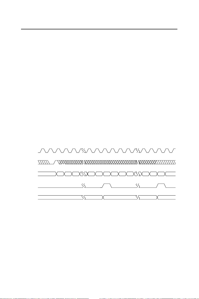
D.2 Mode A Waveforms
Software-Triggered Strobe with No Hardware Gating
Mode A is one of the simplest operating modes. The counter will be
available for counting source edges when it is issued an ARM command.
On each TC the counter will reload from the Load register and automatically disarm itself, inhibiting further counting. Counting will resume
when a new ARM command is issued.
SOURCE
WR
COUNT
VALUE
TC OUTPUT
TC TOGGLED
OUTPUT
ARM
COMMAND
L L-1 L- 2 K+1X K K-1 2 1 0 L
Mode A Waveforms
47 Appendix D
Page 56

D.3 Mode B Waveforms
Software-Triggered Strobe with Level Gating
Mode B is identical to Mode A except that source edges are counted only
when the assigned gate is active. The counter must be armed before
counting can occur. Once armed, the counter will count all source edges
that occur while the gate is active and disregard those edges that occur
while the gate is inactive.
This permits the gate to turn the counting process on and off. On each TC
the counter will reload from the
itself, inhibiting further counting until a new ARM command is issued.
SOURCE
Load register and automatically disarm
WR
GATE
COUNT
VALUE
TC OUTPUT
TC TOGGLED
OUTPUT
ARM
COMMAND
X L L- 1 L-2 K+1 K 2 1 0 L
Mode B Waveforms
PCM-3780 User Manual 48
Page 57

D.4 Mode C Waveforms
Hardware-Triggered Strobe
Mode C is identical to Mode A, except that counting will not begin until a
gate edge is applied to the armed counter. The counter must be armed
before application of the triggering gate edge, while gate edges applied to
a disarmed counter are disregarded.
The counter will start counting on the first source edge after the triggering
gate edge and will continue counting until TC. At TC, the counter will
reload from the
will then remain inhibited until a new ARM command and a new gate
edge are applied in that order.
Note that after application of a triggering gate edge, the gate input will be
disregarded for the remainder of the count cycle. This differs from Mode
B, where the gate can be modulated throughout the count cycle to stop
and start the counter.
SOURCE
Load register and automatically disarm itself. Counting
WR
GATE
COUNT
VALUE
TC OUTPUT
TC TOGGLED
OUTPUT
ARM
COMMAND
X L L- 1 L-2 2 1 0 L
Mode C Waveforms
49 Appendix D
Page 58

D.5 Mode D Waveforms
Rate Generator with No Hardware Gating
Mode D is typically used in frequency generation applications. In this
mode, the gate input does not affect counter operation. Once armed, the
counter will count to TC repetitively. On each TC the counter will reload
itself from the Load register; hence the Load register value determines the
time between TCs. A square wave rate generator may be obtained by
specifying the TC Toggled output mode in the Counter Mode
SOURCE
register.
COUNT
VALUE
TC OUTPUT
TC TOGGLED
OUTPUT
1 0 L 2 1 0
L L- 1 L- 2 22 1 0 L-1 L- 2
Mode D Waveforms
PCM-3780 User Manual 50
Page 59

D.6 Mode E Waveforms
Rate Generator with Level Gating
Mode E is identical to Mode D, except the counter will only count those
source edges that occur while the gate input is active. This feature allows
the counting process to be enabled and disabled under hardware control.
A square wave rate generator may be obtained by specifying the TC toggled output mode.
SOURCE
GATE
COUNT
VALUE
TC OUTPUT
TC TOGGLED
OUTPUT
2 L-1 L-2 K+1 K-1 2 1 0 L
1 0 L K
Mode E Waveforms
51 Appendix D
Page 60

D.7 Mode F Waveforms
Non-Retriggerable One-Shot
Mode F provides a non-retriggerable, one-shot, timing function. The
counter must be armed before it will function. Application of a gate edge
to the armed counter will enable counting. When the counter reaches TC,
it will reload itself from the Load register. The counter will then stop
counting, awaiting a new gate edge.
Note that unlike Mode C, a new ARM command is not needed after TC,
only a new gate edge. After application of a triggering gate edge, the gate
input is disregarded until TC.
SOURCE
GATE
COUNT
VALUE
TC OUTPUT
TC TOGGLED
OUTPUT
X L 1 L
L-1 L-2 2 0
PCM-3780 User Manual 52
Mode F Waveforms
Page 61

D.8 Mode G Waveforms
Software-Triggered Delayed Pulse One-Shot
In Mode G, the gate does not affect the counter's operation. Once armed,
the counter will count to TC twice and then automatically disarm itself.
For most applications, the counter will initially be loaded from the
register either by a LOAD command or by the last TC of an earlier timing
cycle.
Upon counting to the first TC, the counter will reload itself from the
register. Counting will proceed until the second TC, when the counter
will reload itself from the
inhibiting further counting. Counting can be resumed by issuing a new
ARM command.
Specifying the TC Toggled output mode in the Counter Mode register
may generate a software-triggered delayed pulse one-shot. The initial
counter contends control of the delay from the ARM command until the
output pulse starts. The
SOURCE
Load register and automatically disarm itself,
Hold register contents control the pulse duration.
Load
Hold
WR
COUNT
VALUE
TC OUTPUT
TC TOGGLED
OUTPUT
ARM
COMMAND
L L- 1 L-2 2X 0 H H-2 1
1 H-1 2 0 L
Mode G Waveforms
53 Appendix D
Page 62

D.9 Mode H Waveforms
Software-Triggered Delayed Pulse One-Shot with Hardware Gating
Mode H is identical to Mode G except that the gate input is used to qualify which source edges are to be counted. The counter must be armed for
counting to occur. Once armed, the counter will count all source edges
that occur while the gate is active and disregard those source edges that
occur while the gate is inactive. This permits the gate to turn the count
process on and off.
As with Mode G, the counter will be reloaded from the Hold register on
the first TC and reloaded from the Load register and disarmed on the second TC. This mode allows the Gate to control the extension of both the
initial output delay time and the pulse width.
SOURCE
WR
GATE
COUNT
VALUE
TC OUTPUT
TC TOGGLED
OUTPUT
SOURCE
WR
GATE
COUNT
VALUE
TC OUTPUT
TC TOGGLED
OUTPUT
ARM
COMMAND
X L L-1 L-2 K+ 1 K K-1 2 1 0 H H-1 H-2 N+1
N+1 N N-1 2 1 0 L
Mode H
Waveforms
PCM-3780 User Manual 54
Page 63

D.10 Mode I Waveforms
Hardware-Triggered Delayed Pulse Strobe
Mode I is identical to Mode G, except that counting will not begin until a
gate edge is applied to an armed counter. The counter must be armed
before application of the triggering gate edge. Gate edges applied to a disarmed counter are disregarded. An armed counter will start counting on
the first source edge after the triggering gate edge. Countering will then
proceed in the same manner as in Mode G. After the second TC, the
counter will disarm itself. An ARM command and gate edge must be
issued in this order to restart counting.
Note that after application of a triggering gate edge, the gate input will be
disregarded until the second TC. This differs from Mode H, where the
gate can be modulated throughout the count cycle to stop and start the
counter.
SOURCE
WR
GATE
COUNT
VALUE
TC OUTPUT
TC TOGGLED
OUTPUT
ARM
COMMA ND
X L 1 H
L-1 L- 2 2 0
Mode I Waveforms
55 Appendix D
H-1 H-2 2 01 L
Page 64

D.11 Mode J Waveforms
Variable Duty Cycle Rate Generator with No Hardware Gating
Mode J will find the greatest usage in frequency generation applications
with variable duty cycle requirements. Once armed, the counter will
count continuously until it is issued a DISARM command.
On the first TC, the counter will be reloaded from the Hold register.
Counting will then proceed until the second TC at which time the counter
will be reloaded from the Load register. Counting will continue, with the
reload source alternating on each TC, until a DISARM command is
issued to the counter. (The third TC reloads form the Hold register, the
fourth TC reloads form the Load register, etc.)
Specifying the TC Toggled output in the Counter Mode register can generate a variable duty cycle output. The Load and Hold values then directly
control the output duty cycle, with high resolution available when relatively high count values are used.
SOURCE
COUNT
VALUE
TC OUTPUT
TC TOGGLED
OUTPUT
H H-1 H-2 2 1 L L-2 2 1 0 H H-12 1 0 0 L-1 H-2
PCM-3780 User Manual 56
Mode J
Waveforms
Page 65

D.12 Mode K Waveforms
Variable Duty Cycle Rate Generator with Level Gating
Mode K is identical to Mode J except that source edges are only counted
when the Gate is active. The counter must be armed for counting to occur.
Once armed, the counter will count all source edges that occur while the
gate is active and disregard those source edges that occur while the gate is
inactive. This permits the gate to turn the count process on and off.
As with Mode J, the reload source used will alternate on each TC, starting
with the Hold register on the first TC. After the gate modulate the duty
cycle of the output waveform. It can affect both the high and low portions
of the output waveform.
SOURCE
GATE
COUNT
VALUE
TC OUTPUT
TC TOGGLED
OUTPUT
SOURCE
GATE
COUNT
VALUE
TC OUTPUT
TC TOGGLED
OUTPUT
2 1 0 1
N+1 N N-1 2 1 0 H
H H-1 H-2 K+1 K K-1 2 0 L L-1 L-2 N+1
H-1 H-2
Mode K
Waveforms
57 Appendix D
Page 66
D.13 Mode L Waveforms
Hardware-Triggered Delayed Pulse One-Shot
Mode L is similar to Mode J except that counting will not begin before a
gate edge is applied to an armed counter. The counter must be armed
before application of the triggering gate edge; gate edges applied to a disarmed counter are disregarded. The counter will start counting source
edges and counting will proceed until the second TC.
Note that after application of a triggering gate edge, the gate input will be
disregarded for the remainder of the count cycle. This differs from Mode
K, where the gate can be modulated throughout the count cycle to stop
and start the counter. On the first TC after application of the triggering
gate edge, the counter will be reloaded from the Hold register. On the second TC, the counter will be reloaded from the Load register and counting
will stop until a new edge is issued to the counter. Note that unlike Mode
K, new gate edges must be altered every second TC to continue counting.
SOURCE
GATE
COUNT
VALUE
TC OUTPUT
TC TOGGLED
OUTPUT
X L 1 H H-1 H-2 2 01 L
L-1 L- 2 2 0
Mode L Waveforms
PCM-3780 User Manual 58
Page 67

D.14 Mode O Waveforms
Hardware-Triggered Strobe with Edge Disarm
Mode O, shown in Figure O, is identical to Mode C except that the
counter will be disarmed while an inactive-going gate edge is applied to
the counter. And the counter will hold the count value until it is issued a
LOAD command or REST command.
SOURCE
WR
GATE
COUNT
VALUE
TC OUTPUT
TC TOGGLED
OUTPUT
SOURCE
WR
GATE
COUNT
VALUE
TC OUTPUT
TC TOGGLED
OUTPUT
ARM
COMMAND
X L L-1 L-2 2 1 0 L
ARM
COMMAND
X L L-1 L-2
N+2 N+1 N
Mode O Waveforms
59 Appendix D
Page 68

D.15 Mode R Waveforms
Non-Retriggerbale One-Shot with Edge Disarm
Mode R is identical to Mode F except that the counter will be disarmed
while an inactive-going gate edge is applied to the counter. The counter
will hold the count value until it is issued a LOAD command or REST
command.
SOURCE
GATE
COUNT
VALUE
TC OUTPUT
TC TOGGLED
OUTPUT
SOURCE
GATE
COUNT
VALUE
TC OUTPUT
TC TOGGLED
OUTPUT
X L 1 L
L-1 L-2 2 0
L-1 L-2 N+2 NX L N+1
Mode R Waveforms
PCM-3780 User Manual 60
Page 69

D.16 Mode U Waveforms
Hardware-Triggered Delayed Pulse Strobe with Edge Disarm
Mode U is identical to Mode I except that the counter will be disarmed
while the gate and inactive-going gate edge is applied to the counter. The
counter will hold the count value until it is issued a LOAD command or
REST command.
SOURCE
WR
GATE
COUNT
VALUE
TC OUTPUT
TC TOGGLED
OUTPUT
SOURCE
WR
GATE
COUNT
VALUE
TC OUTPUT
TC TOGGLED
OUTPUT
SOURCE
WR
GATE
ARM
COMMA ND
X L 1 H
L-1 L- 2 2 0
ARM
COMMA ND
L-1 L- 2 2 0X L 1 H
ARM
COMMA ND
H-1 H-2 2 01 L
H-1 H-2 N+2 NN+1
COUNT
VALUE
TC OUTPUT
TC TOGGLED
OUTPUT
L-1 L- 2 N+2 NX L N+1
Mode U Waveforms
61 Appendix D
Page 70

D.17 Mode X Waveforms
Hardware-Triggered Delayed Pulse One-Shot with Edge Disarm
Mode X is identical to Mode L except that the counter will be disarmed
while an inactive-going gate edge is applied to the counter. The counter
will hold the count value until it is issued a LOAD command or REST
command.
SOURCE
GATE
COUNT
VALUE
TC OUTPUT
TC TOGGLED
OUTPUT
SOURCE
GATE
COUNT
VALUE
TC OUTPUT
TC TOGGLED
OUTPUT
SOURCE
GATE
COUNT
VALUE
TC OUTPUT
L-1 L-2 2 0X L 1 H H-1 H-2 2 01 L
L-1 L-2 2 0X L 1 H H-1 H-2 N+2 NN+1
L-1 L-2 N+2 NX L N+1
TC TOGGLED
OUTPUT
Mode X Wa veforms
PCM-3780 User Manual 62
 Loading...