

Page 1
MIC-3368
6U-size CompactPCI™ Low
Power Pentium®
Master Single Boa rd
Computer
III 700MHz
Advantech CompactPCI™
Modular Industrial Computer
Page 2

Copyright Notice
This document is copyrighted, 2002. All rights are reserved. The original
manufacturer reserves the right to make improvements to the products described in
this manual at any time without notice. No part of this manual may be reproduced,
copied, translated or transmitted in any form or by any means without the prior
written perm ission of the original manufacturer. Information provided in this
manual is int ende d to be accu rate a nd re liable . Ho weve r, the orig inal m anuf act urer
assumes no responsibility for its use, nor for any infringements upon the rights of
third parties which may result from its use .
Acknowledgements
Award is a trademark of Award Software International, Inc.
Fast EtherChannel (FEC) is a trademark of Cisco Systems, Inc.
IBM, PS/2, OS/2, and VGA are trademarks of International Business Machines
Corporation.
Intel®, Pentium®, and PRO/100+ are trademarks of Intel Corporation.
Windows is a registered trademark of Microsoft Corporation.
NetWare is a trademark of Novell, Inc.
Symbios is a trademark of Symbios Logic Corporation.
PICMG™, CompactPCI™ and the PICMG™, and CompactPCI™ logos are trademarks
of the PCI Industrial Computers Manufacturers Group.
All other product names or trademarks are properties of their respective owners.
CE Notification
The MIC-3368, developed by Advantech CO., LTD., has passed the CE test for
environment specification when shielded cables are used for external wiring. We
recommend the use of shielded cables.
Part No. 2006336800 1st Edition
Printed in Taiwan March 2002
MIC-3368 Series User Manual -- Page
II
Page 3

Product warranty
Advantech warrants to you, the original purchase r, that ea ch of its pro ducts will be
free from defects in materials and workmanship for one year from the date of
purchase. This warranty does not apply to any products which have been repaired or
altered by persons other than repair personnel authorized by Advantech, or which
have been subject to misuse, abuse, accident or improper installation. Advantech
assumes no liability under the terms of this warranty as a consequence of such
events. Because of Advantech’s high qua lity-control standards and rigorous te sting,
most of our customers never need to use our repair service. If an Advantech product
is defective, it will be repaired or replaced at no charge during the warranty period.
For out-of-warranty repairs, you will be billed according to the cost of replacement
materials, service time and freight. Please consult your dealer for more details.
If you think you have a defective product, follow these steps:
1. Collect all the information about the problem encountered. (For example, CPU
speed, Advantech products used, other hardware and software use d, etc.) Note
anything abnormal and list any on-screen messages you get when the problem
occurs.
2. Call your dealer and describe the problem. Please have your manual, product,
and any helpful information readily available.
3. If your product is diagnosed as defec tive, obtain an RMA (return merchandize
authorization) number from your dealer. This allows us to process your return more
quickly.
4. Carefully pack the defective product, a fully-completed Repair and Replacement
Order Card and a photocopy proof of purchase date (such as your sales receipt) in
a shippable container. A product returned without proof of the purc hase date is not
eligible for warranty service.
5. Write the RMA number visibly on the outside of the pac kage and ship it prepaid to
your dealer.
MIC-3368 Series User Manual -- Page
III
Page 4

Packing List
Before installing your board, ensure that the following materials have been
received:
• 1 MIC-3368 all-in-one single board computer
• 1 Utility CD-ROM disc
• 1 Heat sink (Assembled)
• 1 Thermal pad (Assembled)
• 1 Y-type keyboard/mouse cable
• 1 RJ-45 to RS-232 COM port adaptor
• 1 Hard drive isolation pad
• 1 Solder-side cover (Assemb led)
• Several screws
• 1 warranty certificate
• This user's manual
If any of these items are missing or damaged, contact your distributor or sales
representative immediately.
Technical Support and Sales Assistance
If you have any technical questions about the MIC-3368 or any other Advantech
products, please visit our support website at:
• http://support.advantech.com.tw
For more information about Advant ech's products and s ales information, ple ase
visit:
• http://www.advantech.com
.
MIC-3368 Series User Manual -- Page
IV
Page 5

Contents
1. Hardware Configuration ............................................................. 1
1.1 Introduction ............................................................................... 2
1.2 Specifications ............................................................................. 4
1.3 Functional Block Diagram ............................................................ 7
1.4 Jumpers .................................................................................... 8
1.4.1 Jumper Locations ......................................................................... 8
1.4.2 Jumper Settings ........................................................................... 8
1.4.3 Clear CMOS (JP2) ......................... ..................................... ........... 9
1.5 Connectors ............................................................................... 10
1.6 Safety Precautions ..................................................................... 13
1.7 Installing SDRAM (SODIMMs) ...................................................... 14
1.8 Installing CPU and Heat Sink .......... ......................... .................... 15
1.9 Software support ....................... .............................. .................. 16
2. Connecting Peripherals ..... ........................ ....................... .......... 17
2.1 IDE Device (CN10) .................. ......................... .......................... 18
2.2 VGA Display Con nector (CN3) ........... .......................... ................. 18
2.3 PS/2 Keyboard and Mouse Connector (CN5 ) ........................... ....... 18
2.4 Serial Ports (CN1 and CN2) ....... ........................... ....................... 1 9
2.5 Ethernet C onfiguration (CN6 and CN7) .. ............................. .......... 19
2.6 USB Connecto r (CN4) ................... .............................. ................ 20
2.7 Card Instal lation .......................................... .............................. 20
3. Ethernet Software Configuration ................................................ 23
3.1 Introduction ............................................................................. 24
3.2 Utility and Dri vers .......................... ................................. ........... 24
3.3 Installation for Windows NT 4.0 ............. ........................... ........... 27
4. AGP SVGA Setup ..... ....................... ........................ .................. 3 7
4.1 Introduction .............................................................................. 38
4.2 Installati on of SVGA Driver .... .................... ...................... ............ 38
4.3 Installati on for Win dows NT 4 .0 ....... ............ ............. ............. ...... 39.
5. Award BIOS Setup ................................................................... 45
5.1 AWARD BIOS Setup ............................. .................................. .... 46
5.1.1 Entering setup ........... ..................................... ........................ .... 46
5.1.2 Standard CMOS setup ............................ .................................. .... 47
5.1.3 BIOS features set up ............................. ................................. ....... 48
5.1.4 CHIPSET features s etup ............................ ............................ ........ 52
MIC-3368 Series User Manual -- Page
V
Page 6

5.1.5 Power management set up .......................... ........................... ........ 53
5.1.6 PCI configuratio n setup .................... ....................... ...................... 5 4
5.1.7 Load BIOS d efaults ..... .............. ................. ............. ................. ..... 54
5.1.8 Load setup d efaults .......................... ....................... ..................... 54
5.1.9 Integrated Peripherals ............................... ................................... 55
5.1.10 Password setti ng ................................... ................................. .... 55
5.1.11 IDE HDD auto detection ................... ....................... .................... 55
5.1.12 Save & exi t setup ......... ..................... .................... ................. .... 55
5.1.13 Exit witho ut saving ...................... .......................... ..................... 55
A. Programming the Watchdo g Timer ............. ........... ................ ...... 57
A.1 Programming the Watchdog Timer ............. ................................. . 58
B. Pin Assignments ...... ................. ..................... ...................... ..... 61
B.1 VGA Displa y Connector (CN3) .. ...................... ....................... ....... 62
B.2 COM1 and COM2 Serial Ports (CN1 and CN2) ................................... 62
B.3 Keyboard and Mouse Connnector (CN5) .......................................... 63
B.4 USB Connect or (CN 4) ...... ......... .......... .... ........... ......... .......... ....... 6 3
B.5 CPU Fan Power C onn ector (CN8 ) ...... ...... ...... ....... ...... ... ...... ....... .... 64
B.6 Ethernet RJ-45 Con necto rs (C N6 and CN7) .... ....... ...... ...... ....... ... .... 64
B.7 CompactFlash Socket (CN9) ... ............... ................ ................ ....... 65
B.8 System I/O Ports ...... ............. ......... .............. ............. ............. .... 66
B.9 Interrupt A ssignment s ............ ............. .............. ......... ............. .... 67
B.10 1st MB Memo ry M ap ...... ......... .......... ........ .......... ......... .......... .... 67
B.11 J1 connecto r pin assi gnments .. ............. ............. ............ ............. 6 8
B.12 J2 connecto r pin assi gnments .. ............. ............. ............ ............. 6 9
B.13 J3 connecto r pin assi gnments .. ............. ............. ............ ............. 7 0
B.14 J4 connector pi n assign ments fo r M IC-336 8 ....... .... ...... ...... ....... .... 7 1
B.15 J4 connector pi n assign ments fo r M IC-336 8 ....... .... ...... ...... ....... .... 7 2
B.16 J5 connector pin assignments (MIC-3368 only) .............................. 73
MIC-3368 Series User Manual -- Page
VI
Page 7

Figures
Figure 1-1: MIC-3368 functi onal block diagram .................. ......................... 7
Figure 1-2: MIC-3368 jumper and connector locations .................................. 11
Figure 1-3: MIC-3368 front panel connector and indicator locations …………………..12
Figure 1-4: H eat sink installati on .................. ................... .................... ..... 15
Figure 5-1: S etup progr am initi al screen . ............ ............. ............. .......... ... 46
Figure 5-2: CMOS setup screen ......... ...................... ................... .............. 47
Figure 5-3: BI OS features s etup screen.... .................. ................... ............. 48
Figure 5-4: CH IPSET features setup scre en ............... ............... .............. .... 52
Figure 5-5: Power m anagement s etup screen . .............. ................ .............. 5 3
Figure 5-6: PC I configuration scr een .................. ...................... ................. 54
Figure 5-7: Integ rated peripherals ... ......................... .......................... ...... 55
MIC-3368 Series User Manual -- Page
VII
Page 8

Tables
Table 1-1: MIC-3368 jumper descriptions .................. ................................. 8
Table 1-2: Clear CMOS............................................................................. 9
Table 1-3 MIC-3368 connector descripti ons ..................................... .......... 10
Table 2-1: MIC-3368 serial port default settings .... ................... .................. 19
Table B-1: MIC-3368 CRT display conn ector ....................... ....................... 62
Table B-2: MIC-3368 COM1 and com2 seri al ports ........... ................ ........... 62
Table B-3: MIC-3368 keyboard connect or ................. ................... .............. 63
Table B-4: USB connect or .............. ................... ................... .................... 6 3
Table B-5: MIC-3368 CPU fan power connector ........... ..................... .......... 64
Table B-6: MIC-3368 Ethernet RJ-45 connectors .. ......................... ............. 64
Table B-7: MIC-3368 CompactFlash socket .. ....................... ....................... 65
Table B-8: System I/O ports .......... ...................... .......................... .......... 66
Table B-9: Interrup t assignments .............. ........................... .................... 67
Table B-10:1st MB m emory ma p ....... ......... ......... ....... ......... .......... ........... . 67
Table B-11: J1 conn ector pin assignment s ......................... ........................ 6 8
Table B-12: J2 conn ector pin assignment s ......................... ........................ 6 9
Table B-13: J3 conn ector pin assignment s ......................... ........................ 7 0
Table B-14: J4 connector pin assignments fo r MIC-3368 ............ .............. .... 71
Table B-15: J4 connector pin assignments fo r MIC-3368 ............ .............. .... 72
Table B-16: J5 conn ector pin assignment s ......................... ........................ 7 3
MIC-3368 Series User Manual -- Page
VIII
Page 9

1
Hardware
Configuration
MIC-3368 Series User Manual -- Page
1
Page 10

1.1 Introduction
The MIC-3368 is a 6U-size CompactPCI™ all-in-one single board with low power
Pentium®
CompactPCI™
computer telephony and communications. Based on Intel®
III 700MHz CPU on-board which complies with PICMG 2.0 R2.1
specifications. Ta rgeting performance-demanding app lications like
’s 440GX chipset, the
MIC-3368 enhances its performance with 100 MHz front side bus.
High Pe rformance Pentium®
The MIC-3368 integrated an Intel®
the BGA2 package. The low power Pentium®
III Processor
low power Pentium® I II 700MHz processor with
III 700MHz processor has on-chip 256
KB cache providing high performance with low cost. With the support of a 100MHz
CPU bus clock, the MIC-3368 can fulfill customer’s expectations of
high-performance computing capability.
Compact Mechanical Design
The MIC-3368 has many functions on a single board with only one-slot width.
Advantech provides a CPU heat sink spec ially designed for the low power Pentium®
III processor, enabling the MIC-3368 to operate without a cooling fan on the heat
sink. It only needs external cooling air from the chassis fans for ventilation. This
enables the MIC-3368 to use a Pentium®
III CPU within a mere 1-slot wide space.
Single P2P Bridge
The MIC-3368 with single PCI-to-PCI Bridge (Intel® DEC21155) is applicable up to
8-slot enclosure (MIC-3032/MIC-3038) and drive up to seven bus master PCI slots.
PMC (PCI Mezzanine Card) IEEE1386.1 Compliant
The MIC-3368 support up to two PMC sites and compliant with PICMG 2.3 (PCI
Mezzan ine Card ) specific ation. These two 32-bit PMC inter face pr ovides fr ont acce ss
capability by PMC modules for various function demanding.
Complete I/O Functions
The MIC-3368 offers all the I/O functions of an industrial computer with the rugged
Eurocard form factor. Since two PMC sites knockouts most area of front panel, only
few I/O connectors are available on the fro nt panel including one Ethernet interface,
one serial port, and one PS/2 K/B and mouse. The rest of I/O have fully connected
to the rear I/O module via user-define connector (J3 ~ J5) on the backplane. These
I/O contain two Fast Ethernet interfaces, secondary serial port, one USB port, one
VGA connector, and one PS/2 keyboard/mouse connector. The front panel also has
MIC-3368 Series User Manual -- Page
2
Page 11

a reset button and LEDs for power status, HDD operation and Ethernet
communication. The built-in high speed IDE controller provides two separate IDE
channels with Ultra DMA/33 mode. The user-defined J3 connector is designed to
support up to four IDE devices and two floppy drives. These drives can simply be
connected to the backplane or to the rear tr ansition board for easy service and
maintenance.
Meets Industrial and Comput er-T elephony Applications Requirements
The MIC-3368 is designed for use in mission critical applications. It accepts a
CompactFlash™ memory card on either the rear transition board or MIC-3368 itself,
thus eliminating the need to use a fragile rotating hard drive. A watchdog timer can
automatically reset the system if the syste m stops due to a program bug or EMI. The
two-layer front panel design complies with IEEE 1101.10. Connectors are firmly
screwed to the front panel, and the replaceable shielding gasket is attached to the
panel edge. This reduces emissions and gives better protection against external
interference.
1.2 Specifications
Standard SBC Functions
• CPU: BGA2 Low Power Pentium®
• BIOS: Award 2 Mb flash memory
• Chipset: Inte l®
440GX / 440BX Chipset
• Front Side Bus Clock: 100 MHz for Intel®
• Bus Interface: 32-bit, 33 MHz, PICMG 2.0 compliant
• 2nd level cache: CPU built-in 256 KB (Pentium®III) on die
• RAM: Two 144-pin SO-DIMM sockets. Support PC-100 SDRAMs with memory
capacity up to 1GB (MIC-3368) and 512MB for MIC-3368B. Support ECC.
• Enhanc ed ID E in ter fa ce: T wo channe ls handles up to 4 IDE HDDs or other IDE
devices via J3 connector. Supports PIO mode 4 and Ultra DMA/33 mode.
• Floppy disk drive interface: Supports up to two floppy disk drives through the
J3 connector
• Serial ports: Two RS-232 ports with 16C550 compatible UARTs
• USB interfac e: One USB connector with fuse protection. Complies with USB
specification 1.0
III Coppermine CPU 700 MHz
Pentium® III CP U
• Keyboa rd/mouse connectors: One 6-pin mini-DIN connector on the front panel
• Watchdog timer: Can generate a system reset. Software enabled/disabled. Time
interval is from 1 to 63 seconds, jumperless with run-time setup.
MIC-3368 Series User Manual -- Page
3
Page 12

PCI-to-PCI Bridge
• Controlle r chip: One (MIC-3368) Intel® DEC 21155 transparent co ntroller chips,
drives up to seven PCI master peripherals
• Supports up to seven bus masters on each bus segment
• Provides seven pairs of GNT# and REQ# signals on each bus segment
10/100Base-TX Ethernet Interface
• Controller chips: Two Intel® 82559 Fast Ethernet controller chips
• Dual LAN ports (RJ-45)
• 10 Mbps or 100 Mbps auto-switching
AGP VGA Interfac e
• Controller: Intel® C&T 69030
• AGP 1.0 compliant, 66 MHz
• Display memory: On-chip 4MB SDRAM
• Display Resolution Number of Colors:
640 x 480, 800 x 600,
1024 x 768, 1280 x 1024 256 (8 bits)
640 x 480, 800 x 600, 1024 x 768 65, 536 (16 bits)
640 x 480, 800 x 600 16.8 million ( 24 bits)
640 x 480, 800 x 600 16.8 million ( 32 bits).
Optional Rear I/O Boards
• For MIC-3368: MIC-3308
• For MIC-3368B: MIC-3308
Mechanical and Environmental Specifications
• Operating temperature: 0 ~ 55° C (32 ~ 131° F)
• Storage Temperature: -20 ~ 80° C (-4 ~ 176° F)
• Humidity (operating and storage): 5 ~ 95% (non-condensing)
• Power Consumption: +5 V@ 2.1 A; +3.3 V @ 2.5 A; +12 V @ 640 mA
• Board size: 233.35 x 160 mm (6U size), 1-slot (4 TE) wide
• Weight: 0.8 kg (1.8 lb)
• Shock: 20 G (operating); 50 G (storage/transit)
• Random vibration: 1.5 Grms.
1.3 Functional Block Diagram
MIC-3368 Series User Manual -- Page
4
Page 13

Figure 1-1: MIC-3368 functional block diagram.
MIC-3368 Series User Manual -- Page
5
Page 14

1.4 Jumpers
1.4.1 Jumper Locations
The MIC-3368 provides a jumper (JP2) for configuring your board for specific
applications other than the default settings. Table 1-1 lists the jumper function.
Figure 1-2 illustrates the jumper location. Read this section carefully before
changing the jump setting on your MIC-3368 card.
Table 1-1: MIC-3368 jumper descriptions
Number Function
JP1 Clear CMOS
JP2 CF Mode (CF Master / Slave)
JP3 Hot-swap connector (For MIC-3368C only)
JP6 Primary PCI VIO
JP7 Secondary PCI VIO
JP8 PMC Module voltage
1.4.2 Jumper Settings
This section tells how to set the jumpers to configure your card. It gives the card
default configuration and your options for each jumper. After you set the jumpers
and install the card, you will also need to run the BIOS Setup program (discussed in
Chapter 6) to configure the serial port addresses, floppy/hard disk drive types and
system operating parameters. Connections, such as hard disk cables, appear in
Chapter 2. For the locations of each jumper, see the bo ard layout diagram depicted
earlier in this chapt er.
You configure your card to match the needs of your application by setting jumpe rs.
A jumpe r is the sim p le s t k in d o f e le c t ric switc h . I t consist s of t w o me t a l p in s a nd a
small metal cap (often protected by a plastic cover) that slides over the pins to
connect them. To "close" a jumper you connect the pins with the cap. To "open" a
jumper you remove the cap. Sometimes a jumper will have three pins, labeled 1, 2
and 3. In this case you connect either pins 1 and 2 or 2 and 3.
MIC-3368 Series User Manual -- Page
6
Page 15
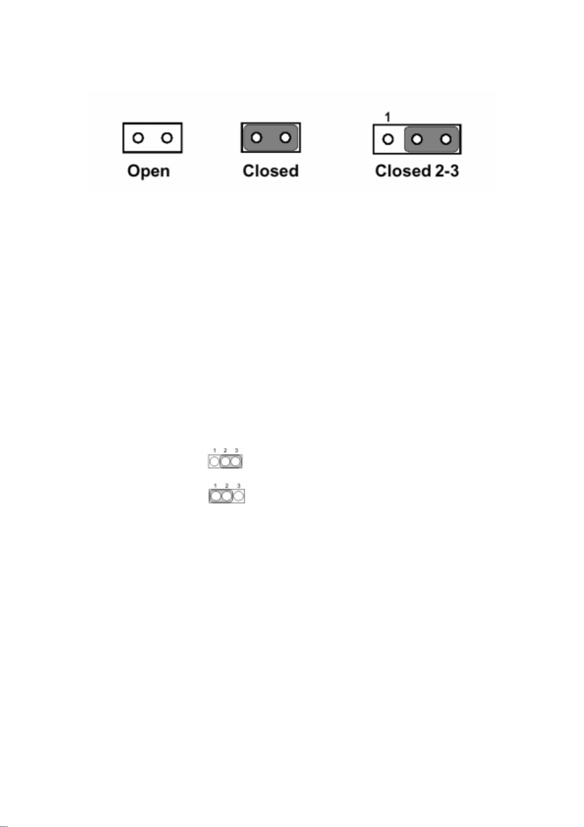
The jumper se ttings are schematica lly depicted in this manual as follows:
You may find a pair of needle-nose pliers useful for setting the jumpers.
If you have any doubts about the best hardware co nfiguration for your application,
contact your local distributor or sales representative before you make any changes.
1.4.3 Clear CMOS (JP1)
This jumper is used to erase CMOS data and reset syste m BIOS information. Follow
the procedures below to clear the CMOS.
1. Turn off the system.
2. Close jumper JP2 (2-3) for about 3 seconds.
3. Close jumper JP2 (1-2).
4. Turn on the system. The BIOS is reset to its default setting.
Table 1-2: Clear CMOS
CMOS JP1
Clear
Normal (default)
1.5 Connectors
On-board connectors link to external devices such as hard disk drives, keyboards, or
floppy drives, etc. Table 1-3 lists the function of each connector and Figure 1-2 and
Figure 1-3 illustrate each connector location. Chapter 2 gives instructions for
connecting external devices to your card.
Table 1-3 MIC-3368 connector descriptions
Number Function
CN1 Secondary IDE (CF)
CN2 Primary IDE
CN4 SODIMM Socket
CN5 Ethernet RJ-45 Connec tor
MIC-3368 Series User Manual -- Page
7
Page 16

CN7 COM1 RJ-45 Connector
CN8 CPU fan power connector
CN9 CompactFlash socket (optional)
J1/J2 Primary CompactPCI™ bus
J3 Rear I/O trans ition
J4 (MIC-3368) Rear I/O transition
J4/J5 (MIC-3368) Secondary C ompactPCI™ bus
LED1 HDD LED and Power LED
SW1 Reset switch
Please refer to Appendix B for pin assignments.
Figure 1-2: MIC-3368 jumper and connector locations.
Figure 1-3: MIC-3368 front panel connector and indicator locations
1.6 Safety Precautions
Follow these simple precautions to protect yourself from harm and the products
MIC-3368 Series User Manual -- Page
8
Page 17

from damage.
1. To avoid electric shock, always disconnect the power from your PC chassis before
you work on it. Don't touch any components on the CPU card or other cards while
the PC is on.
2. Disconnect power before making any configuration changes. The sudden rush of
power as you con nect a jumper or install a card may damage sensitiv e electronic
components.
3. Always ground yourself to remove any static charge before you touch your CPU
card. Be particularly careful not to touch the chip connectors. Modern integrated
electronic devices, especially CPUs and memory chips, are extremely sensitive to
static electric discharges and fields. Keep the card in its antistatic packaging when it
is not installed in the PC, and place it on a static dissipative mat when you are
working with it. Wear a grounding wrist strap for continuous protection.
1.7 Installing SDRAM (SODIMMs)
The MIC-3368 provides two 144-pin SODIMM sockets. Each socket accepts either
16, 32, 64, 128 or 256 MB SDRAM (for MIC-3368B). Also the 512MB SODIMM
support for MIC-3368. The sockets can be filled in any combination with SODIMMs
of any size, giving a total memory capacity between 16 and 512 MB. If only one
SODIM M module is required, it can be installed in eith er SODIMM socket.
Since the MIC-3368 can operate at 66 or 100 MHz, we recommend using
PC100-compliant SODIMMs. To enable the chipset's Error Checking and Correction
(ECC) function, please use SODIMMs which support the ECC function. The
procedure for installing SODIMMs appears below. Please follow these steps
carefully.
1. Ensure that all power supplies to the system are switched off.
2. Install the SODIMM module. Install the SODIMM so that its gold pins point down
into the SODIMM socket.
3. Slip the SODIMM into the socket at a 45 degree angle and carefully fit the bottom
of the card against the connectors.
4. Gently push the SODIMM into the socket until the clips on the ends of the
SODIMM sockets snap int o place.
5. Check to ensure that the SODIMM is correctly seated and all connector contacts
touch. The SODIMM should not move ar ound in its socket.
NOTE: The SODI MM modules can only fit into sockets o ne way, in
accordance with the keyed notches along the bottom edge of the modules.
Their gold pins must point down into the SODIMM socket.
MIC-3368 Series User Manual -- Page
9
Page 18

1.8 Installing CPU Heat Sink
The MIC-3368 integrates Intel® Low Power Pentium® III Coppermine CPU. In order
to meet critical environmental conditions and the physical space of the MIC-3368 at
the same time, Advantech designed a heat sink to fulfill its primary needs. Please
refer to Figure 1-4 for an illustration of the heat sink used for the MIC-3368.
The small aluminum plate is default fastened on the CPU in the factory.
Figure 1-4: Heat sink installation.
Figure 1-5: Complete assembly with heat sink and hard disk
MIC-3368 Series User Manual -- Page
10
Page 19

1.9 Software support
The MIC-3368 comes with a utility CD-ROM disc, which includes drivers and utility
programs of Ethernet and SVGA interfaces. The 440GX and 440BX chipset may not
be recognized by some old-versioned Windows 95. Please visit Intel®’s website to
download the required files:
http://developer.intel.com/design/chipsets/drivers/inf_update.htm
.
MIC-3368 Series User Manual -- Page
11
Page 20

2
Connecting
Peripherals
MIC-3368 Series User Manual -- Page
12
Page 21

2.1 IDE Device (CN10)
The MIC-3368 provides two IDE (Integrated Device Electronics) channels via the J3
connector to the rear transition board (RIO-3308 for MIC-3368). Four IDE drives
can be connected to the MIC-3368 through the rear transition board. Users can
connect two IDE drives to each IDE channel. If two drives are installed on one
channel, remember to set one as the master and the other one as the slave. You
may do this by setting the jumpers on the drives. Refer to the documentation that
came with your drive for more information. A jumper diagram usually appears on
the top side of a hard disk drive.
Warning: Plug the other end of the cable into the drive with pin #1 on the cable
corresponding to pin #1 on the drive. Improper connection will damage the drive.
2.2 VGA Display Connector (CN3)
The MIC-3368 provides a VGA chipset (CHIPs 69030) built-in display for high
performance application. The RIO-3308's CN3 is a DB-15 connector for VGA monitor
input. Pin assignments for the VGA display are detailed in Appendix B.
2.3 PS/2 Keyboard and Mouse Connector (CN5)
The MIC-3368 provides a 6-pin mini-DIN connector (CN5) on the front panel for
connection of PS/2 keyboard and PS/2 mouse. The MIC-3368 comes with a cable to
convert from the single 6-pin mini-DI N connector to a double PS/2 keyboard
connector and PS/2 mouse connector. Since these two connectors are identical,
please, follow the icons on the cable to plug the keyboard and the mouse into their
correct connecto rs.
2.4 Serial Ports (CN1 and CN2)
The MIC-3368 offers two serial ports: COM1 and COM2, both in RS-232. With
limited front panel access, only COM1 can be connected via a RJ-45 to RS-232
adaptor and COM2 interface has to via rear I/O module (RIO-3308) for implement.
These ports allow users to connec t to serial devices (a mouse, printers, e tc.) or a
communication network. You can select the address for each port (For example,
3F8H [COM1], 2F8H [COM2]) or disable it, using the BIOS Advanced Setup program,
covered in Chapter 5. Different devices implement the RS-232 standard in different
ways. If you are having problems with a serial device, be sure to check the pin
assignments for the connector. T he IRQ and address range for both ports are fixed.
However, if you wish to disable the port or change the se parameters later, you c an
do this in the system BIOS setup. The table below shows the settings for the
MIC-3368 board's ports:
Table 2-1: MIC-3368 serial port default settings
MIC-3368 Series User Manual -- Page
13
Page 22

Port Address Default
COM1 3F8, 3E8 3F8/IRQ4
COM2 2F8, 2E8 2F8/IRQ3
2.5 Ethernet Configuration (CN6 and CN7)
The MIC-3368 is equipped with dual high performance 32-bit PCI-bus Fast Ethernet
interfaces which are fully compliant with IEEE 802.3u 10/100Base-TX specifications.
It is supported by all major network operating systems and is 100% Novell NE-2000
compatible. One on-board RJ-45 jacks provide convenient co nnec tion to the
network. Another one has to go through RIO module as well as COM port. The
medium type can be configured via the software program included on the utility
CD-ROM disc. (See Chapter 3 for detailed information.).
2.6 USB Connector (CN4)
The MIC-3368 provides one USB (Universal Serial Bus) interface via the rear I/O
module panel. The USB interface gives complete plug and play, hot attach/detach
for up to 127 external devices. The MIC-3368 USB interface complies with USB
specification rev. 1.0 and is fuse protected. The USB interface can be disabled in the
system BIOS setup. The USB controller default is "Enabled" but the USB keyboard
support default is "Disabled".
2.7 PMC Connector (CN4)
The MIC-3368 support two PMC (PMC Mezzanine Card) modules on PCI bus 0. The
MIC-3368 support two PMC (PMC Mezzanine Card) modules on PCI bus 0. This
32-bit, 3.3 V PCI bus is available at connectors J11 and J12. J14 is used for PMC rear
panel I/O per the PMC specification (IEEE P1386.1/Draft 2.2). Front panel access is
provided for the PMC interface. Signals from PMC modules that support rear panel
I/O are routed out the rear of the board thro ugh backplane connec tor J3. A second
PMC position is also available as an option. This position replaces the EIDE drive
capability, front panel video, and Serial Port access. This 32-bit, 3.3 V PCI bus is
available at connectors J21 and J22. J24 is used for PMC rear panel I/O per the PMC
specificatio n ( IEEE P1 3 86 . 1 /D raft 2. 2) . Rear panel I/O fr o m t his PMC s ite is rout ed
out the rear of the board through backplane connector J5.
2.8 Card Installation
The CompactPCI™ connectors are firm and rigid, and r equire careful handling while
plugging and unplugging. Improper installation of a card can easily damage the
backplane of the chassis. The inject/eject handles of MIC-3368 help you install and
MIC-3368 Series User Manual -- Page
14
Page 23

remove the card easily and safely. Follow the procedure below to install the
MIC-3368 into a chassis:
To install a card:
1. Hold t he c ar d ver tica lly . Be sur e th at th e ca rd is poin tin g in t he cor re ct dir ec tio n.
The components of the card should be pointing to the right-hand side.
2. Pull out both handles to unlock it.
Caution: Keep your fing ers away from the hinge to preve nt your fingers from getting
pinched.
3. Insert the card into the chassis by sliding the upper and lower edges of the card
into the card guides.
4. Push the card into the slot gently by sliding the card along the card guide until the
handles meet the rectangular holes of the cross rails. Note: If the card is correctly
positioned and has been slid all the way into the chassis, the handle should match
the rectangular holes. If not, remove the card fro m the c ard guide and re pe at step
3 again. Do not try to install a card by forcing it into the chassis.
5. Pull the upper handle down and lift the lower handle up to push the card into
place.
6. Secure the card by pushing in the red handle to lock it into place.
To remove a card:
1. Unscrew the screws on the front panel.
2. Lift the upper handle up and press the lower handle down to release the card from
the backplane.
3. Slide the card out.
Figure 2-1: Installing the card into the chassis
MIC-3368 Series User Manual -- Page
15
Page 24

3
Ethernet
Software
Configuration
MIC-3368 Series User Manual -- Page
16
Page 25

3.1 Introduction
The MIC-3368 has two on-board high-performance fast Ethernet interfaces which
comply with IEEE 802.3/802.3u for 10Base-T and 100 Base-TX data rates.
The module uses two Intel®
and is c ompatible with the In tel®
Ethernet channel design provides several options for increasing throughput and
fault tolerance when running Windows NT 4. 0 or NetWare 4.1x and ne wer versions
of these, includes:
• Adapter Fault Tolerance (AFT) - provides automatic redundancy for your Ethernet
channel. If the primary channel fails, the secondary takes over.
• Adaptive Load Balancing (ALB) - creates a team of 2 channels to increase
transmission throughput. Also includes AFT and ALB. This function works with any
100BASE-TX switch.
• Fast EtherChannel (FEC) - creates a team of 2 to 4 channels to increase
transmission and reception throughput. Also includes AFT. This funct ion requires a
Cisco switch with FEC capability. The MIC-3368 comes with drivers for a wide
variety of networks and operating systems. The MIC-3368 is an excellent choice for
operation in standalone and harsh industrial env ironments.
82559 fast Ethernet controllers with integrated PHY
PRO/100+ Server and Client Adapter. The dual
3.2 Utility and Drivers
The MIC-3368's on-board Ethernet interface supports all major network operating
systems. The installation instructions and drivers for different operating systems
are located in the following directories of the utility CD-ROM disc:
General Inf ormation:
• \MIC3368\LAN\README.TXT: General infor mation about the drivers.
For Microsoft Windows:
• \MIC3368\LAN\INFO\MS\MS.TXT: Installation instructions for Microsoft
Windows
• \MIC3368\LAN\E100BNT.SYS (NDIS 4.0), \MIC3368\LAN\
OEMSETUP.INF: Drivers for Windows NT 4.0
• \MIC3368\LAN\E100B.SYS (NDIS 3), \MIC3368\LAN\
OEMSETUP.INF: Drivers for Windows NT 3.51
• \MIC3368\LAN\NET82557.INF: Drivers f or Windows 98
• \MIC3368\LAN\E100BNT.SYS (NDIS 4.0),
\MIC3368\LAN\NET82557.INF: Drivers for Windows 95
• MIC3368\LAN\W FW\E100B.38 _, \MIC3368\LA N\WFW\OEM SETUP.INF:
Drivers for Windows 3.1
MIC-3368 Series User Manual -- Page
17
Page 26

For Novell NetWare
• \MIC3368\LAN\INFO\NETWARE\NETWARE.TXT: Installation instructions
for Novell NetWare
• \MIC3368\LAN\NWSERVER\3X4X.OLD\E100B.LAN: Drivers for NetWare
3.12 and 4.10
• \MIC3368\LAN\NWSERVER\311LAN\E100B.LAN: Drivers for NetWare
3.11
• \MIC3368\LAN\OS2\E100BODI.SYS: Drivers for NetWare OS/2 ODI Client
• \MIC3368\LAN\DOS\E100BODI.COM: Drivers for DOS ODI Client
For UNIX
• \MIC3368\LAN\INFO\UNIX\UNIX.TXT: Installation instructions for UNIX
For Other Operating Systems
• \MIC3368\LAN\INFO\OTHER\OTHER.TXT: Installation instructions for other
operating systems
• \MIC3368\LAN\DOS\E100B.DOS: Drivers for IBM LAN support for AS/400
and NetWare (for LANSUP).
• \MIC3368\LAN\DOS\E100BODI.COM: Drivers for IBM LAN support for
AS/400 and NetWare (for ODINSUP)
• \MIC3368\LAN\OS2\E100B.OS2: Drivers for LAN server (OS/2 driver)
• \MIC3368\LAN\DOS\E100B.DOS: Drivers for LAN server (DOS driver)
• \MIC3368\LAN\DOS\E100B.DOS: Drivers for BANYAN NDIS workstation
• \MIC3368\LAN\DOS\E100B.DOS: Drivers for LANTASTIC 6.0
• \MIC3368\LAN\DOS\E100B.DOS: Driver s f or g ene r al N DI S 2 .X (D O S dr iv er )
• \MIC3368\LAN\OS2\E100B.OS2: Drive rs fo r ge ner al NDI S 2. X (OS /2 d riv er )
Before installing drivers, please refer to the installation instructions of each
operating system.
Note: Do not use the driver recommended by the Windows 95/98/NT Add New
Hardware wizard. Choose the driver from the utility CD-ROM disc.
Note: Operating system vendors may post driver updates on their web sites. Please
visit the web sites of OS vendors to download updated drivers.
3.3 Installation for Windows NT 4.0
Before installing; create a new folder [ ], \MIC3368\LAN\, in your disk drive, and
download all files from the directory, \MIC3368\LAN\, on the utility CD-ROM to it.
1. In the Windows NT screen, select "Start", click "Settings". Click the "Control
Panel" item and choose "Network".
2. Click "Yes".
3. Click "Wire d to the Network", or users may choo se "Remote access to the
MIC-3368 Series User Manual -- Page
18
Page 27

network" if applicable.
4. Click "Select from list" .
5. Click "Have Disk".
6. Type in "E:\MIC3368\LAN" in the blank column and click "OK". (E: your hard disk
drive).
7. Click "OK".
8. Click "Next".
9. Click "Next".
10. Click "Next".
11. Click "Next".
12. Insert Windows NT source disc in drive E. Type "E:\I386" in the blank column or
any other directory that contains the Windows NT files. Click "Continue".
13. Wait for the installation to finish.
14. Complete the settings with users' network settings. Click "OK".
15. Click "Next".
16. Click "Next".
17. Click "Yes" to restart the computer and enable the changes to take effect.
MIC-3368 Series User Manual -- Page
19
Page 28

4
AGP-SVGA
Setup
4.1 Introduction
The MIC-3368 uses an Intel® C&T 69030 chipset as its AGP VGA controller. The
MIC-3368 Series User Manual -- Page
20
Page 29

VGA controller has an integrated 4 MB SDRAM operating at 83 MHz, and can drive
CRT displays with resolutions up to 1600 x 1200 @ 64 K colors. It supports
interlaced and non-interlaced analog monitors (color and monochrome VGA) in
high-resolution modes while maintaining complete IBM VGA compatibility. Digital
monitors (i.e. MDA, CGA, and EGA) are NOT supported. Multiple frequency
(multi-sync) monitors are handled as if they were analog monitors .
4.2 Installation of SVGA Driver
The MIC-3368 is supplied with a utility CD-ROM disc that holds the necessary file for
setting up the VGA display under the directory \MIC3368\VGA. The contents and
pathnames of this directory are listed below:
• MIC3368\VGA\Win31: VGA utility for Windows 3.1
• MIC3368\VGA\Win95\w95500: VGA utility for Windows 95
• MIC3368\VGA\Win98\w98600: VGA utility for Windows 98
• MIC3368\VGA\WINNT: Utility for Window s NT 4.0
• MIC3368\VGA\OS2: VGA utility for OS/2
Complete the following steps to install the VGA driver. Follow the procedures in the
flow chart that apply to the operating system you are using with your MIC-3368.
4.3 Installation for Windows NT 4.0
1. Select "Settings" "Control Panel" from the "Start" menu.
2. Click "Display".
3. Select the "Settings" tab and click the "Display Type" button.
4. Click "Change" button in the "Adapter Type" block.
5. Click "Have Disk" button in the "Change Display" Windows.
6. Insert the utility CD-ROM disc in drive E. Type "E:\MIC3368\VGA\WINNT” in the
blank column. Click "OK".
7. Click "OK".
8. Click "OK" to install the VGA driver.
9. Wait for installation to finish.
10. Click "OK" and restart the computer to enable the change to take effect.
MIC-3368 Series User Manual -- Page
21
Page 30

5
Award
BIOS
Setup
MIC-3368 Series User Manual -- Page
22
Page 31

5.1 AWARD BIOS Setup
Figure 5-1: Setup program initial screen
Award's BIOS ROM has a built-in Setup program that allows users to modify the
basic system configu ration. This type of information is stored in battery-backed
CMOS so that it retains the Setup information when the power is turned off.
5.1.1 Entering Setup
Turn on the computer and check for the "patch code". If there is a number assigned
to the patch code, it means that the BIOS support yo ur CPU. If there is no number
assigned to the patch code, please contact Advantech' s applicat ion engineer to
obtain an up-to-date patch code file. This will ensure that your CPU's system status
is valid. After ensuring that you have a number assigned to the patch code, press
<DEL> and you will immediately be allowed to enter Setup.
5.1.2 Standard CMOS Setup
Choose the "STANDARD CMOS SETUP" option from the INITIAL SETUP SCREEN
Menu, and the screen below will be displayed. This standard setup menu allows
users to configure system components such as date, time, hard disk drive, floppy
drive, display, and memory.
MIC-3368 Series User Manual -- Page
23
Page 32

Figure 5-2: CMO S set u p screen
.
5.1.3 BIOS Features Setup
The "BIOS FEATURES SETUP" screen will appear after the BIOS FEATURES SETUP
item from the CMOS SETUP UTILITY Menu was chosen. This screen allows the user
to configure the MIC-3368 according to his particular require ments. Below are some
major items that are provided in the BIOS FEATURES SETUP screen:
Figure 5-3: BIOS features se tup screen
Virus Warning
During and after the system boots up, any attempt to write to the boot sector or
partition table of the hard disk drive will ha lt the system. If this happens, a warning
message will be displayed. You can run the anti-v irus program to locate the problem.
If Virus Warning is disabled, no warning message will appear if anything attempts to
access the boot sector or hard disk partition.
CPU Internal Cache/External Cache
Depending on the CPU/chipset design, these options can speed up memory access
MIC-3368 Series User Manual -- Page
24
Page 33

when enabled.
Quick Power On Self Test
This option speeds up the Power-On Self Test (POST) conducted as soon as the
computer is turned on. When enabled, the BIOS shortens or skips some of the items
during the test. When it disabled, normal POST procedures res ume.
Boot Sequence
This function determines the sequence in which the computer will search the drives
for the disk operating system (i.e. DOS). The default value is "C, A, SCSI". The
following options are available:
A: Computer will boot from the A (floppy) disk drive
C: Computer will boot from the C (hard) disk drive
CDROM: Computer will boot from the CD-RO M disc drive
SCSI: Computer will boot from the SCSI drive
D: Computer will boot from the D drive
E: Computer will boot from the E drive
F: Computer will boot from the F drive
LS120: Computer will boot from the LS-120 driv e
Boot Up Floppy Seek
During POST, the BIOS will determine if the floppy disk drive installed has 40 or 80
tracks. The 360 KB type has 40 tracks while the 720 KB, 1.2 MB, and 1.44 MB all
have 80 tracks.
Enabled BIOS searches the floppy drive to det ermine if it has 40 or 80 tracks. N ote that BIOS
cannot differentiate 720 KB , 1.2 MB, and 1.44 MB type drives as they all ha v e 80 tracks .
Disabled BIOS will not se arch for the floppy drive type by tra ck num ber. Note that th ere will
not be any warning message if the drive installed is 360 KB. l
Boot Up NumLock Status
The default is "On".
On: Keypad boots up to number keys.
Off: Keypad boots up to arrow keys.
Boot Up System Speed
High: Sets the speed to high
Low: Sets the speed to low
IDE HDD Block Mode
Enabled: Enable I DE HDD Block Mode. B IOS will detec t the block size of the HDD and sen d a
block command automatically.
Disabled: Disable IDE HDD Block Mode
Gate A20 option
Normal: The A20 signal is controlled by the keyboard controller or chipset hardware
MIC-3368 Series User Manual -- Page
25
Page 34

Fast: (Default: Fast) The A20 sign al is controlled by Port 92 or by a chipset speci fic method.
Typematic Rate Setting
The typematic rate determines the characters per second accepted by the computer.
Typematic Rate setting enables or disables the typematic rate.
Typematic Rate (Char/Sec)
BIOS accept the following input values (character/second) for Typematic Rate: 6, 8,
10, 12, 15, 20, 24, and 30.
Typematic Delay (msec)
When holding down a key, the Typematic Delay is the time interval between the
appearance of the first and second characters. The input values (msec) for this
category are: 250, 500, 750, and 1000.
Security Option
This setting determines whether the system will boot if the password is denied,
while limiting access to Setup.
System: The system will n ot boot, and access to Setup will be denied if th e correct password
is not entered at the prompt.
Setup: The system will bo ot, but access to Setu p will be denied if the cor rect password is n ot
entered at the prompt.
Note: To disable security, select PASSWORD SETTING in the main menu. At this
point, you will be asked to enter a password. Simply hit the <ENTER> key to disable
security. When security is disabled, the system will boot, and you can enter Setup
freely.
OS Select for DRAM>64 MB
This setting is for use under the OS/2 operating system.
Video BIOS Shadow
This setting determines whether the video BIOS will be copied to RAM, which is
optional according to the chipset design. When enabled, Video Shadow increases
the video speed.
C8000 - CFFFF Shadow/DC000-DFFFF Shadow
These settings determine whether optional ROM will be copied to
RAM in blocks of 16 KB.
Enabled: Optional shadow is enabled
Disabled: Optional shadow is disabled.
5.1.4 CHIPSET Features Setup
Choosing the "CHIPSET FEATURES SETUP" option from the INITIAL SETUP SCREEN
Menu causes the screen below to be displayed. This sample screen contains the
manufacturer's default values for the MIC-3368.
MIC-3368 Series User Manual -- Page
26
Page 35

Figure 5-4: CH IPSET featu res setup screen
VGA Shared Mem o ry Size
Shared memory architecture can support 0.5 MB, 1MB, 1.5 MB, 2 MB, 3 MB, 3.5 MB
and 4 MB of system memory.
5.1.5 Power Management Setup
The power management setup controls the CPU cards' "green" features. The
following screen shows the manufacturer's default values.
Figure 5-5: Power management setup screen
Power Management
This option allows you to determine if the values in power management are disabled,
user-defined, or predefined.
MIC-3368 Series User Manual -- Page
27
Page 36

HDD Power Management
You can choose to turn the HDD off after one of the time intervals listed, or when the
system is in Suspend mode. If in a power saving mode, any access to the HDD will
wake it up.
Note: The HDD will not power down if the Power Management option is disabled.
IRQ Activity
IRQ can be set independently. Activity on any enabled IRQ will wake up the system.
5.1.6 PNP/PCI Configuration Setup
Figure 5-6: PNP/PCI configuration screen
5.1.7 Integrated Peripherals
Figure 5-7: Integrated periph era l s
MIC-3368 Series User Manual -- Page
28
Page 37

Note: If you enable the IDE HDD block mode, the enhanced IDE driver will be
enabled.
5.1.8 Load Setup Defaults
"LOAD SETUP DEFAULTS" loads the values required by the system for maximum
performance.
5.1.9 Password Setting
To change, confirm, or disable the password, choose the "PASS-WORD SETTING"
option form the Setup main menu and press [Enter]. The password can be at most
8 characters long. Remember, to enable this feature. You must first select the
Security Option in the BIOS FEATURES SETUP to be either "Setup" or "System."
Pressing [Enter] again without typing any characters can disable the password
setting function.
5.1.10 IDE HDD Auto Detection
"IDE HDD AUTO DETECTION" automatically self-detects the hard disk type.
5.1.11 Save & Exit Setup
If you select this and press the [Enter] key, the values entered in the setup utilit ies
will be recorded in the CMOS memory of the chipset. The microprocessor will check
this every time you turn your system on and compare this to what it finds as it
checks the system. This record is required for the system to operate.
5.1.12 Exit Without Saving
Selecting this option and pressing the [Enter] key lets you exit the Setup program
without recording any new values or changing old ones.
MIC-3368 Series User Manual -- Page
29
Page 38

A
Programming
Watchdog Timer
MIC-3368 Series User Manual -- Page
30
Page 39

A.1 Programming the Watchdog Timer
To pro gra m t he w atc hd og tim er , yo u m us t wr ite a pr og r am w hic h wr it es a v alue t o
I/O port address 443 (hex). This output value represents time interval. The value
range is from 01 (hex) to FF (hex), and the related time interval is 1 sec. to 255 sec.
Data Time Interval
01 1 sec.
02 2 sec.
03 3 sec.
04 4 sec.
••
••
••
3F 63 sec.
After data entry, your program must refresh the watchdog timer by rewriting the
I/O port 443 and 043 (hex) while simultaneously setting it. When you want to
disable the watchdog timer, your program should read I/O port 043 (hex). The
following example shows how you might program the watchdog timer in BASIC:
10 REM Watchdog timer example program
20 OUT &H443, data REM Start and restart the watchdog
30 GOSUB 1000 REM Your application task #1,
40 OUT &H443, data REM Reset the timer
50 GOSUB 2000 REM Your application task #2,
60 OUT &H443, data REM Reset the timer
70 X=INP (&H043) REM, Disable the watchdog timer
80 END
1000 REM Subroutine #1, your application task
••
••
••
1070 RETURN
2000 REM Subroutine #2, your application task
••
••
••
2090 RETURN.
MIC-3368 Series User Manual -- Page
31
Page 40

B
Pin Assignments
MIC-3368 Series User Manual -- Page
32
Page 41

B.1 System Slot J1 Connector
Table A-1: System slot J1 connector
Pin Z A B C D E F
25 GND +5V REQ64# ENUM# +3.3V +5V GND
24 GND AD[1] +5V V(I/O) AD[0] ACK64# GND
23 GND +3.3V AD[4] AD[3] +5V AD[2] GND
22 GND AD[7] GND +3.3V AD[6] AD[5] GND
21 GND +3.3V AD[9] AD[8] M66EN C/BE[0]# GND
20 GND AD[12] GND V(I/O) AD[11] AD[10] GND
19 GND +3.3V AD[15] AD[14] GND AD[13] GND
18 GND SERR# GND +3.3V PAR C/BE[1]# GND
17 GND +3.3V SDONE SBO# GND PERR# GND
16 GND DEVSEL# GND V(I/O) STOP# LOCK# GND
15 GND +3.3V FRAME# IRDY# BD/SEL# TRDY# GND
12-14 Key Area
11 GND AD[18] AD[17] AD[16] GND C/BE[2]# GND
10 GND AD[21] GND +3.3V AD[20] AD[19] GND
9 GND C/BE[3]# N/C AD[23] GND AD[22] GND
8 GND AD[26] GND V(I/O) AD[25] AD[24] GND
7 GND AD[30] AD[29] AD[28] GND AD[27] GND
6 GND REQ# GND +3.3V CLK AD[31] GND
5 GND N/C N/C RST# GND GNT# GND
4 GND N/C Healthy# V(I/O) INTP INTS GND
3 GND INTA# INTB# INTC# +5V INTD# GND
2 GND TCK +5V TMS N/C TDI GND
1 GND +5V -12V TRST# +12V +5V GND
#: Low active
MIC-3368 Series User Manual -- Page
33
Page 42

B.2 System Slot P2 Connector
Table A-2: System slot P2 connector
Pin Z A B C D E F
22 GND GA4 GA3 GA2 GA1 GA0 GND
21 GND CLK6 GND N/C RSV RSV GND
20 GND CLK5 N/C N/C GND N/C GND
19 GND N/C GND N/C N/C N/C GND
18 GND N/C N/C N/C GND N/C GND
17 GND N/C GND PRST# REQ6# GNT6# GND
16 GND N/C N/C DEG# GND N/C GND
15 GND N/C GND FAL# REQ5# GNT5# GND
14 GND AD[35] AD[34] AD[33] GND AD[32] GND
13 GND AD[38] GND V(I/O) AD[37] AD[36] GND
12 GND AD[42] AD[41] AD[40] GND AD[39] GND
11 GND AD[45] GND V(I/O) AD[44] AD[43] GND
10 GND AD[49] AD[48] AD[47] GND AD[46] GND
9 GND AD[52] GND V(I/O) AD[51] AD[50] GND
8 GND AD[56] AD[55] AD[54] GND AD[53] GND
7 GND AD[59] GND V(I/O) AD[58] AD[57] GND
6 GND AD[63] AD[62] AD[61] GND AD[60] GND
5 GND C/BE[5]# 64EN# V(I/O) C/BE[4]# PAR64# GND
4 GND V(I/O) N/C C/BE[7]# GND C/BE[6]# GND
3 GND CLK4 GND GNT3# REQ4# GNT4# GND
2 GND CLK2 CLK3 SYSEN# GNT2# REQ3# GND
1 GND CLK1 GND REQ1# GNT1# REQ2# GND
#: Low active
Note: GA[4...0] shall be used for geographic addressing on the backplane
MIC-3368 Series User Manual -- Page
34
Page 43

B.3 System and Peripheral Slots J3 Connector
Table A-3: System slot J3 connector
Pin Z A B C D E F
19
18
17
16
15
14
13
12
11
10
9
8
7
6
5
4
GND
GND
GND
GND
GND
GND
GND
GND
GND
GND
GND
GND
GND
GND
GND
GND
USBD1+ USBD1- USBD0+ USBD0- N/C
LPA_DA+ LPA_DA- GND LPA_DC+ LPA_DCLPA_DB+ LPA_DB- GND LPA_DD+ LPA_DDLPB_DA+ LPB_DA- GND LPB_DC+ LPB_DCLPB_DB+ LPB_DB- GND LPB_DD+ LPB_DD-
+3.3V +3.3V +3.3V +5V +5V
PMC1IO5 PMC1IO4 PMC1IO3 PMC1IO2 PMC1IO1
PMC1IO10 PMC1IO9 PMC1IO8 PMC1IO7 PMC1IO6
PMC1IO15 PMC1IO14 PMC1IO13 PMC1IO12 PMC1IO11
PMC1IO20 PMC1IO19 PMC1IO18 PMC1IO17 PMC1IO16
PMC1IO25 PMC1IO24 PMC1IO23 PMC1IO22 PMC1IO21
PMC1IO30 PMC1IO29 PMC1IO28 PMC1IO27 PMC1IO26
PMC1IO35 PMC1IO34 PMC1IO33 PMC1IO32 PMC1IO31
PMC1IO40 PMC1IO39 PMC1IO38 PMC1IO37 PMC1IO36
PMC1IO45 PMC1IO44 PMC1IO43 PMC1IO42 PMC1IO41
PMC1IO50 PMC1IO49 PMC1IO48 PMC1IO47 PMC1IO46
GND
GND
GND
GND
GND
GND
GND
GND
GND
GND
GND
GND
GND
GND
GND
GND
GND
3
2
1
GND
GND
PMC1IO55 PMC1IO54 PMC1IO53 PMC1IO52 PMC1IO51
PMC1IO60 PMC1IO59 PMC1IO58 PMC1IO57 PMC1IO56
#: Low active
PMCVIO PMC1IO64 PMC1IO63 PMC1IO62 PMC1IO61
GND
GND
GND
MIC-3368 Series User Manual -- Page
35
Page 44

B.4 System Slot J4 Connector
Table A-4: System slot J4 connector
Pin Z A B C D E F
25 GND
24 GND
23 GND
22 GND
21
20
19
18
17
16
15
GND
GND
GND
GND
GND
GND
GND
12-14
11
10
9
8
GND
GND
GND
GND
GND HHCS1- HHIRQ HRST1PRI N/C
HHIOW- HHDRQ- HHRDY HHCS3- HHACK-
IID15 HHDA0 HHDA1 HHIOR- HHDA2
IID10 IID11 IID12 IID13 IID14
IID5 IID6 IID7 IID8 IID9
IID0 IID1 IID2 IID3 IID4
PDASP# PDIAG N/C RED GREEN
N/C N/C N/C GND BLUE
HLEDIO# N/C 2RXD232 SCL CRT-H
N/C 1RXD232 N/C SDA CRT-V
N/C N/C N/C NTX2 N/C
Key Area
NRLSD1 NDTR1 NRI1 NDSR2 NRX2
NCTS1 NDTR2 N/C NTX1 NDSR1
NCTS2 NRTS2 NRTS1 NRLSD2 NRX1
RX1 NRI2 -RTS2 TX1 -RTS1
GND
GND
GND
GND
GND
GND
GND
GND
GND
GND
GND
GND
GND
GND
GND
7
6
5
4
3
2
1
GND
GND
GND
GND
GND
GND
GND
TX2 RX2 STB- AFD- LPTD2
INIT- LPTD1 ERR- LPTD0 LPTD6
LPTD5 LPTD4 LPTD3 SLIN- SLCT
PE BUSY ACK- LPTD7 RWC#
TRAK0# WP# RDATA# HEAD# DSKCHG#
MOB# DIR# STEP# WD# WE#
N/C INDEX# MOA# DSB# DSA#
GND
GND
GND
GND
GND
GND
GND
MIC-3368 Series User Manual -- Page
36
Page 45

B.5 System Slot J5 Connector
Table A-5: System slot J5 connector
Pin Z A B C D E F
22
21
20
19
18
17
16
15
14
13
12
11
10
9
8
7
GND
GND
GND
GND
GND
GND
GND
GND
GND
GND
GND
GND
GND
GND
GND
GND
LANTX+2 LANRX+2 KDAT HIRQ15 HRST1SEC
LANTX-2 LANRX-2 KCLK HSDACK# HSCS1#
GND AUXVCC RSTIN HSIORDY HSCS3#
LANTX+ LANRX+ MDAT HSDIOW# HSDREQ
LANTX- LANRX- MCLK HSDIOR# HSDA2
GND AUXVCC HSDD15 HSDA0 HSDA1
HSDD10 HSDD11 HSDD12 HSDD13 HSDD14
HSDD5 HSDD6 HSDD7 HSDD8 HSDD9
HSDD0 HSDD1 HSDD2 HSDD3 HSDD4
PMC2IO5 PMC2IO4 PMC2IO3 PMC2IO2 PMC2IO1
PMC2IO10 PMC2IO9 PMC2IO8 PMC2IO7 PMC2IO6
PMC2IO15 PMC2IO14 PMC2IO13 PMC2IO12 PMC2IO11
PMC2IO20 PMC2IO19 PMC2IO18 PMC2IO17 PMC2IO16
PMC2IO25 PMC2IO24 PMC2IO23 PMC2IO22 PMC2IO21
PMC2IO30 PMC2IO29 PMC2IO28 PMC2IO27 PMC2IO26
PMC2IO35 PMC2IO34 PMC2IO33 PMC2IO32 PMC2IO31
GND
GND
GND
GND
GND
GND
GND
GND
GND
GND
GND
GND
GND
GND
GND
GND
6
5
4
3
2
1
GND
GND
GND
GND
GND
GND
PMC2IO40 PMC2IO39 PMC2IO38 PMC2IO37 PMC2IO36
PMC2IO45 PMC2IO44 PMC2IO43 PMC2IO42 PMC2IO41
PMC2IO50 PMC2IO49 PMC2IO48 PMC2IO47 PMC2IO46
PMC2IO55 PMC2IO54 PMC2IO53 PMC2IO52 PMC2IO51
PMC2IO60 PMC2IO59 PMC2IO58 PMC2IO57 PMC2IO56
RIOINSTALL# PMC2IO64 PMC2IO63 PMC2IO62 PMC2IO61
GND
GND
GND
GND
GND
GND
MIC-3368 Series User Manual -- Page
37
Page 46

B.6 EIDE Connector (CN1)
43 1
44 2
Table A-13: Hard Disk Drive Connector
Pin Signal Pin Signal
1 PRST# 2 GND
3 PID7 4 PID8
5 PID6 6 PID9
7 PID5 8 PID10
9 PID4 10 PID11
11 PID3 12 PID12
13 PID2 14 PID13
15 PID1 16 PID14
17 PID0 18 PID15
19 GND 20 N/C
21 PDRQ# 22 GND
23 PIOW# 24 GND
25 PIOR# 26 GND
27 PRDY 28 Pull low
29 PACK# 30 GND
31 PIRQ 32 N/C
33 PDA1 34 Pull low
35 PDA0 36 PDA2
37 PCS1# 38 PCS3#
39 HDD_LED 40 GND
41 VCC 42 VCC
43 GND 44 GND
B.7 Ethernet RJ-45 Connectors (CN5)
Table B-6: MIC-3368 Ethernet RJ-45 connectors
Pin Signal
1 TX+
2 TX3 RX+
4 N/C
MIC-3368 Series User Manual -- Page
38
Page 47

5 N/C
6 RX7 N/C
8 N/C
B.8 VGA Display connector (CN6)
5 1
15 11
Table A-15: CRT display connector
Pin Signal
1 RED
2 GREEN
3 BLUE
4 N/C
5 GND
6 GND
7 GND
8 GND
9 VGAVCC
10 GND
11 N/C
12 SDA
13 HSYNC
14 VSYNC
15 SCL
B.9 RJ45-COM1 Serial Ports (CN7)
Table B-2: MIC-3368 COM1 and com2 serial ports
Pin Signal
1 NRLSD1
2 NRX1
3 NTX1
MIC-3368 Series User Manual -- Page
39
Page 48

4 NDTR1
5 GND
6 NDSR1
7 NRTS1
8 NCTS1
B.10 Fan Module Connectors (CN8)
1 2 3
Table A-10: Fan Module Connectors
Pin Assignment
1 Fan speed
2 +12V
3 GND
B.11 CompactFlash Socket (CN9)-Optional
Table B-7: MIC-3368 CompactFlash socket
Pin Signal Pin Signal
1 GND 26 N/C
2 ID3 27 ID11
3 ID4 28 ID12
4 ID5 29 ID13
5 ID6 30 ID14
6 ID7 31 ID15
7 HCS1- 32 HCS38 GND 33 N/C
9 GND 34 HIOR10 GND 35 HIOW11 GND 36 N/C
12 GND 37 HIRQ
13 VCC 38 VCC
14 GND 39 SANDISK
15 GND 40 N/C
16 GND 41 -HRST1
17 GND 42 HRDY
18 GDA2 43 N/C
MIC-3368 Series User Manual -- Page
40
Page 49

19 HDA1 44 N/C
20 HDA0 45 SANLED
21 ID0 46 N/C
22 ID1 47 ID8
23 ID2 48 ID9
24 N/C 49 ID10
25 N/C 50 GND.
B.12 System I/O Ports
Table B-8: System I/O ports
Addr. range (Hex) Device
000-01F DMA controller
020-021 Interrupt controller 1, mas ter
022-023 Chipset address
040-05F 8254 timer
060-06F 8042 (keyboard control ler)
070-07F Real-time clock, non-maskable interrupt (NMI)
mask
080-09F DMA page register
0A0-0BF Interrupt controll er 2
0C0-0DF DMA controller
0F0-0F8 Math co-process or
1F0-1F7 Fixed disk
2F8-2FF Serial port 2
3B0-3BB VGA adapter
3C0-3DF VGA adapter
3F0-3F5 Diskette contr oller
3F8-3FF Serial port 1.
B.13 Interrupt Assignments
Table B-9: Interrupt assignments
Interrupt# Interrupt source
IRQ 0 Interval timer
IRQ 1 Keyboard
IRQ 2 Interrupt from controller 2 (casc ade)
IRQ 8 Real-time clock
IRQ 9 VGA
IRQ 10 Available
MIC-3368 Series User Manual -- Page
41
Page 50

IRQ 11 Available
IRQ 12 PS/2 mouse
IRQ 13 INT from co-processor
IRQ 14 Fixed disk controller
IRQ 15 Available
IRQ 3 Serial communication port 2
IRQ 4 Serial communication port 1
IRQ 5 Available
IRQ 6 Diskette controller (FDC )
IRQ 7 Available
B.14 1st MB Memory Map
Table B-10:1st MB memory map
Addr. range (Hex) Device
F000h - FFFFh System ROM
CC00h - EFFFh Unused
CA00h - CBFFh Used
C000h - C9FFh Expansion ROM
B800h - BFFFh CGA/EGA/VGA text
B000h - B7FFh Unused
A000h - AFFFh EGA/V GA graph ics
0000h - 9FFFh Base memory.
MIC-3368 Series User Manual -- Page
42
 Loading...