

Page 1

MIC-3365
6U-sized Intel Pentium III/Celeron CPU
board for
CompactPCI™CompactPCI™
CompactPCI™
CompactPCI™CompactPCI™
Page 2

Copyright Notice
This document is copyrighted, 2000. All rights are reserved. The
original manufacturer reserves the right to make improvements to the
products described in this manual at any time without notice.
No part of this manual may be reproduced, copied, translated or
transmitted in any form or by any means without the prior written
permission of the original manufacturer. Information provided in this
manual is intended to be accurate and reliable. However, the original
manufacturer assumes no responsibility for its use, nor for any
infringements upon the rights of third parties which may result from
its use.
Acknowledgements
Award is a trademark of Award Software International, Inc.
Fast EtherChannel (FEC) is a trademark of Cisco Systems, Inc.
IBM, PS/2, OS/2, and VGA are trademar ks of International Business
Machines Corporation.
Intel, Pentium, Celeron, and PRO/100+ are trademarks of Intel
Corporation.
Windo ws is a registered trademark of Microsoft Corporation.
NetW are is a trademark of No vell, Inc.
Symbios is a trademark of Symbios Logic Corporation.
PICMG™, CompactPCI™ and the PICMG™, and CompactPCI™
logos are trademarks of the PCI Industrial Computers Manufacturers
Group.
All other product names or trademarks are properties of their
respective owners.
CE Notification
The MIC-3365, developed by Advantech CO., LTD., has passed the
CE test for environment specification when shielded cables are used
for external wiring. We recommend the use of shielded cables.
Part No. 2006336510 2nd Edition
Printed in Taiwan September 2000
Page 3

Product warranty
Advantech warrants to you, the original purchaser, that each of its
products will be free from defects in materials and workmanship for
one year from the date of purchase.
This warranty does not apply to any products which have been
repaired or altered by persons other than repair personnel authorized
by Advantech, or which have been subject to misuse, abuse, accident
or improper installation. Advantech assumes no liability under the
terms of this warranty as a consequence of such events.
Because of Advantech’s high quality-control standards and rigorous
testing, most of our customers never need to use our repair service. If
an Advantech product is defective, it will be repaired or replaced at no
charge during the warranty period. For out-of-warranty repairs, you
will be billed according to the cost of replacement materials, service
time and freight. Please consult your dealer for more details.
If you think you have a defective product, follow these steps:
1. Collect all the information about the problem encountered. (For
example, CPU speed, Advantech products used, other hardware
and software used, etc.) Note anything abnormal and list any onscreen messages you get when the problem occurs.
2. Call your dealer and describe the problem. Please have your
manual, product, and any helpful information readily available.
3. If your product is diagnosed as defective, obtain an RMA (return
merchandize authorization) number from your dealer. This allows
us to process your return more quickly.
4. Carefully pack the defective product, a fully-completed Repair
and Replacement Order Card and a photocopy proof of purchase
date (such as your sales receipt) in a shippable container. A
product returned without proof of the purchase date is not eligible
for warranty service.
5. Write the RMA number visibly on the outside of the package and
ship it prepaid to your dealer.
Page 4

Packing List
Before installing your board, ensure that the following materials have
been received:
• One MIC-3365 all-in-one single board computer
• One utility CD-ROM disc
• One 6-pin mini-DIN to PS/2 keyboard and PS/2 mouse cable
• One heat sink plate
• One optional bracket for mounting on-board hard disk drive and
floppy disk drive
• One hard disk drive (IDE) interface cable (44-pin)
• One 26-pin FPC for floppy drive
• One warranty certificate
• This user's manual
If any of these items are missing or damaged, contact your distributor
or sales representative immediately.
Technical Support and Sales Assistance
If you have any technical questions about the MIC-3365 or any other
Advantech products, please visit our support website at:
• http://www .advantech.com.tw/support
For more information about Advantech's products and sales information, please visit:
• http://www .advantech.com
Page 5

Contents
Chapter 1 Hardware Configuration..................................... 1
1.1 Introduction .....................................................................................2
1.2 Specifications...................................................................................3
1.2.1 Standard SBC functions ........................................................................3
1.2.2 VGA interface .......................................................................................4
1.2.3 Ultra 2 SCSI Interface (MIC-3365 and MIC-3365F) ...........................4
1.2.4 Mechanical and environmental specifications .......................................4
1.3 Safety Precautions...........................................................................5
1.4 Function Block Diagram ................................................................6
1.5 Board Dimensions ........................................................................... 7
1.6 Jumpers............................................................................................8
1.6.1 Jumper Locations ..................................................................................8
1.6.2 Jumper Settings .....................................................................................9
1.6.3 Clear CMOS (JP5) ..............................................................................10
1.7 Connectors .....................................................................................11
1.8 Front Panel Connectors and Indicators.......................................13
1.9 Installing SDRAM (DIMMs) .........................................................14
1.10 Installing CPU heat sink and HDD, FDD brackets .....................16
1.11 Software Support ...........................................................................18
CHapter 2 Connecting Peripherals .................................. 19
2.1 IDE Device (CN12) ........................................................................20
2.2 Floppy Drive (CN11).....................................................................20
2.3 VGA Display Connector (CN2)..................................................... 21
2.4 Parallel Port Connector (CN1).....................................................21
2.5 PS/2 Keyboard and Mouse Connector (CN7)..............................21
2.6 Serial Ports (CN13 and CN6)........................................................21
2.7 Ethernet Configuration (CN4 and CN5) ......................................22
2.8 USB Connector (CN8) ...................................................................22
Page 6

2.9 Ultra 2 SCSI Interface...................................................................23
2.10 Card Installation ...........................................................................23
Chapter 3 Ethernet Software Configuration ..................... 25
3.1 Introduction...................................................................................26
3.2 Utility and Drivers.........................................................................26
3.3 Installation for Windows NT 4.0 ..................................................29
Chapter 4 AGP VGA Setup .................................................. 3 9
4.1 Introduction ...................................................................................40
4.2 Installation of SVGA Driver.........................................................40
4.3 Installation for Windows NT 4.0 ..................................................41
Chapter 5 SCSI Software Configuration .......................... 47
5.1 Introduction ...................................................................................48
5.2 Utility and Drivers.........................................................................48
5.3 Installation for Windows NT 4.0 ..................................................50
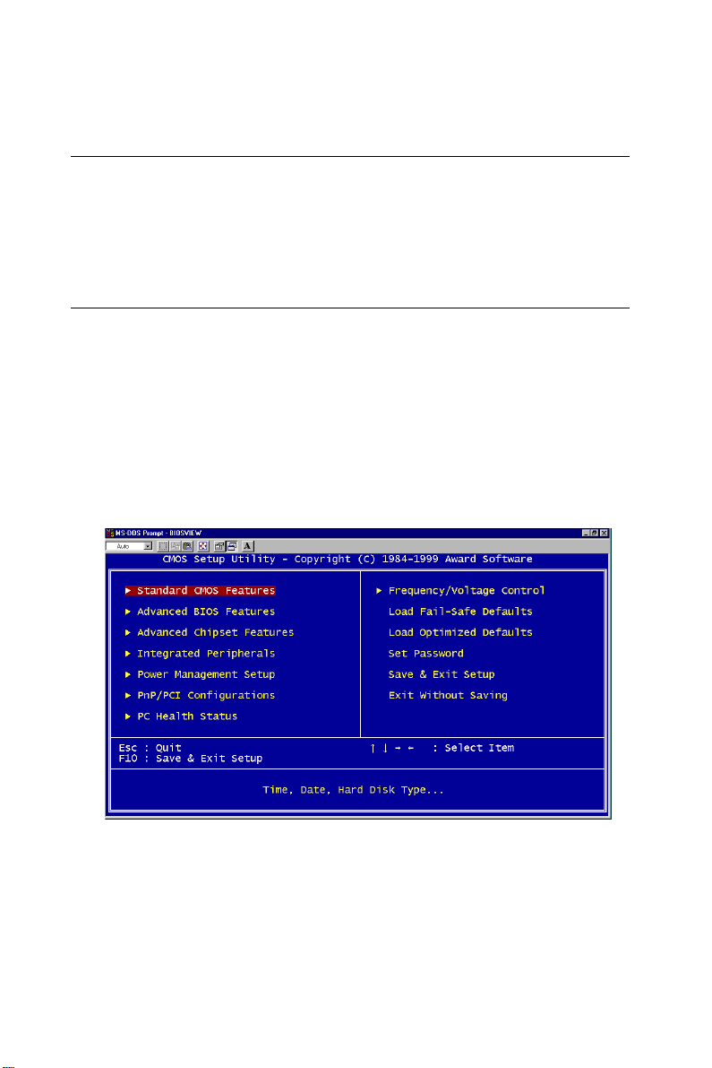
Chapter 6 Award BIOS Setup .............................................. 59
6.1 Introduction...................................................................................60
6.2 Entering Setup ...............................................................................60
6.3 Standard CMOS Features .............................................................61
6.4 Advanced BIOS Features..............................................................62
6.5 CHIPSET Features Setup ............................................................. 65
6.6 Integrated Peripherals..................................................................65
6.7 Power Management Setup ............................................................66
6.8 PnP/PCI Configurations ...............................................................67
6.9 Load Optimized Defaults ..............................................................68
6.10 Set Password ..................................................................................69
6.11 Save & Exit Setup ...........................................................................70
6.12 Exit Without Saving .......................................................................71
Appendix A Programming the Watchdog Timer................ 73
A.1 Programming the Watchdog Timer.................................................74
Page 7

Appendix B Pin Assignments.............................................. 77
B.1 VGA Display Connector (CN2) ......................................................78
B.2 Keyboard and Mouse Connnector (CN7).....................................78
B.3 COM1 and COM2 Serial Port (CN13 and CN6) .........................79
B.4 USB Connector (CN8) ...................................................................80
B.5 Ethernet RJ-45 Connector (CN4 and CN5)..................................80
B.6 Parallel Port Connector (CN1) .....................................................81
B.7 IDE Connector (CN12) ..................................................................82
B.8 Floppy Drive Connnector (CN11) ................................................83
B.9 System I/O Ports ............................................................................84
B.10 DMA Channel Assignments...........................................................85
B.11 Interrupt Assignments ...................................................................85
B.12 1st MB Memory Map....................................................................86
B.13 J1 connector pin assignments.......................................................87
B.14 J2 connector pin assignments.......................................................88
B.15 J3 connector pin assignments.......................................................89
B.16 J4 connector pin assignments.......................................................90
B.17 J5 connector pin assignments.......................................................91
Page 8

Tables
T able 1-1: MIC-3365 jumper descriptions ..............................................8
T able 1-2: Clear CMOS.......................................................................10
T able 1-3: MIC-3365 connector descriptions ....................................... 1 1
T able 1-4: Recommended SDRAM .....................................................15
T able 2-1: MIC-3365 serial port default settings .................................. 22
T able B-1: MIC-3365 CRT display connector.......................................7 8
T able B-2: MIC-3365 keyboard connector ...........................................78
T able B-3: MIC-3365 COM1 and COM2 serial port.............................. 79
T able B-4: MIC-3365 USB1/USB2 connector ......................................8 0
T able B-5: MIC-3365 Ethernet RJ-45 connector .................................. 80
T able B-6: MIC-3365 parallel port connector .......................................81
T able B-7: MIC-3365 IDE connector.................................................... 82
T able B-8: MIC-3351 floppy drive connector ........................................83
Table B-9: System I/O ports ............................................................... 84
T able B-10: DMA channel assignments.............................................. 8 5
T able B-1 1: Interrupt assignments ......................................................85
Table B-12: 1st MB memory map ....................................................... 86
T able B-13: J1 connector pin assignments .........................................87
T able B-14: J2 connector pin assignments .........................................88
T able B-15: J3 connector pin assignments .........................................89
T able B-16: J4 connector pin assignments .........................................90
T able B-17: J5 connector pin assignments .........................................91
Page 9

Figures
Figure 1-1: MIC-3365 function block diagram........................................6
Figure 1-2: MIC-3365 board dimensions ...............................................7
Figure 1-3: MIC-3365 jumper locations .................................................8
Figure 1-4: MIC-3365 connector locations ..........................................12
Figure 1-5: MIC-3365 front panel connector and indicator locations ....13
Figure 1-6: Heat sink installation for 1 slot wide solution ....................16
Figure 1-7: Heat sink installation for 2 slot wide solution ....................17
Figure 2-1: Installing the card into the chassis ...................................24
Figure 6-1: Initial Setup screen.......................................................... 60
Figure 6-2: Standard CMOS Features screen.................................... 61
Figure 6-3: Advanced BIOS Features screen.....................................62
Figure 6-4: Advanced Chipset Features screen .................................65
Figure 6-5: Integrated Peripherals screen ........................................... 66
Figure 6-6: Power Management Setup screen ................................... 67
Figure 6-7: PnP/PCI Configurations screen .......................................6 8
Figure 6-8: Load Optimized Defaults screen ....................................... 68
Figure 6-9: Set Password screen ....................................................... 6 9
Figure 6-10: Save & Exit Setup screen............................................... 70
Figure 6-1 1: Exit Without Saving screen.............................................71
Page 10

Page 11

Hardware Configuration
1
CHAPTER
Page 12

1.1 Introduction
The MIC-3365 is a 6U-sized Intel® Pentium® III/CeleronTM CPU board
and complies with PICMG 2.0 R2.1 CompactPCITM specifications.
The MIC-3365 supports both FC-PGA Intel® Pentium® III Coppermine processors and Intel® CeleronTM processors.
The MIC-3365 is available in three versions: MIC-3365, MIC-3365D,
and MIC-3365F.
Model COM USB SCSI
MIC-3365 1 1 Yes 1 1-slot MIC-3365D 1 1 - 2 1-slot MIC-3365F 2 2 Yes 1 2-slot Yes
PCI-to-PCI
bridge
width
On-board
HDD & FDD
Please check which version of the MIC-3365 you have on hand.
Some of the functions in this manual may not be applicable to some
versions. The MIC-3365 supports rear transition board and is best
performed with the MIC-3302. Please refer to the MIC-3302's manual
for more detailed information.
2 MIC-3365 User's Manual
Page 13

1.2 Specifications
1.2.1 Standard SBC functions
• CPU: Intel® Socket 370 Pentium® III Coppermine CPU up to 700
MHz, Intel® Socket 370 CeleronTM CPU up to 566 MHz
• BIOS: Award BIOS (Intel® FWH 4 Mb)
• Chipset: Intel® 810
• System bus frequency: 100/66 MHz
• Bus interface: 32-bit, 33 MHz, PICMG 2.0 compliant
• L2 cache: CPU built-in 256 KB (Pentium® III) or 128 KB
(Celeron™) on die
• RAM: Two 168-pin DIMM sockets support up to 512 MB SDRAM
at 100 MHz, unbuffered
• EIDE interface: Handles up to 4 IDE HDDs or other IDE devices.
Supports PIO mode 4 and Ultra DMA/33, Ultra DMA/66 mode (via
J3 connector)
• FDD interface: Supports up to two floppy disk drives (via J3
connector)
• Parallel port: Configured to LPT1, LPT2, LPT3 or disabled.
Supports multi-mode parallel port (SPP/ECP/EPP)
• Serial ports: Two RS-232 ports with 16C550 UARTs. MIC-3365
and MIC-3365D provides one serial port, and MIC-3365F provides
two serial ports on the front panel
• PCI W atchdog timer (MIC-3365D only): Can gener ate a system
reset. Time interval is from 1 to 63 seconds, jumperless with runtime setup. To program the watchdog timer, refer to Appendix A,
"Programming the Watchdog Timer".
• Ethernet: Dual Intel® 82559 Fast Ethernet Controller Chips, 10/
100 Base-TX with RJ-45 connectors
• Keyboard/mouse connector: One 6-pin mini-DIN connector on the
front panel
Chapter 1 Hardware Configuration 3
Page 14

• USB interface: T w o USB connectors with fuse protection.
MIC-3365 and MIC-3365D provides one USB connector and
MIC-3365F provides two USB connectors on the front panel
• PCI-to-PCI bridge: One/T w o Intel® DEC 21150 PCI bus controller
chips, drive up to 7/14 PCI bus master peripherals. MIC-3365 and
MIC-3365F support 7 PCI bus masters and MIC-3365D supports 14
PCI bus masters.
1.2.2 VGA interface
• Controller: Chipset built-in VGA display
• Display resolution: Supports non-interlaced CRT monitor
resolutions up to 1024 x 768 x 16-bit color for 3D graphics, and
1600 x 1200 x 8-bit color for 2D graphics. 24-bit color up to
1280 x 1024.
1.2.3 Ultra 2 SCSI Interface (MIC-3365 and MIC-3365F)
• Controller: Symbios SYM53C895
• Supports 16-bit Low Voltage Differential (LVD) and Single Ended
(SE) signaling
• Performs Ultra 2 SCSI L VD synchronous. T ransfers as fast as
80 MB/s
• Available on the rear transition board (MIC-3302) via J5 connector
1.2.4 Mechanical and environmental specifications
• Board size: 233.35 x 160 mm (6U size), MIC-3365 and
MIC-3365D is 1-slot (4TE) wide, and MIC-3365F is 2-slot (8TE)
wide
• Max. power requirements: +5 V (4.75 ~ 5.25 V) @ 6.38 A (Intel
CeleronTM 500 MHz)
• Operating temperature: 0 ~ 60° C (32 ~ 158° F)
• Storage temperature: -20° C ~ 80° C(-4 ~ 176° F)
4 MIC-3365 User's Manual
®
Page 15

• Humidity (operating and storage): 5 ~ 95% (non-condensing)
• Board weight: 0.8 kg (1.8 lb)
• Shock: 20 G (operating); 50 G (storage/transit)
• Random vibration: 1.5 Grms
1.3 Safety Precautions
Follow these simple precautions to protect yourself from harm and the
products from damage.
1. To avoid electrical shock, always disconnect the power from your
PC chassis before you work on it. Don't touch any components on
the CPU card or other cards while the PC is on.
2. Disconnect power before making any configuration changes. The
sudden rush of power as you connect a jumper or install a card
may damage sensitive electronic components.
3. Always ground yourself to remove any static charge before you
touch your CPU card. Be particularly careful not to touch the chip
connectors. Modern integrated electronic devices, especially
CPUs and memory chips, are extremely sensitive to static electrical discharges and fields. Keep the card in its antistatic packaging
when it is not installed in the PC, and place it on a static dissipative mat when you are working with it. Wear a grounding wrist
strap for continuous protection.
Chapter 1 Hardware Configuration 5
Page 16
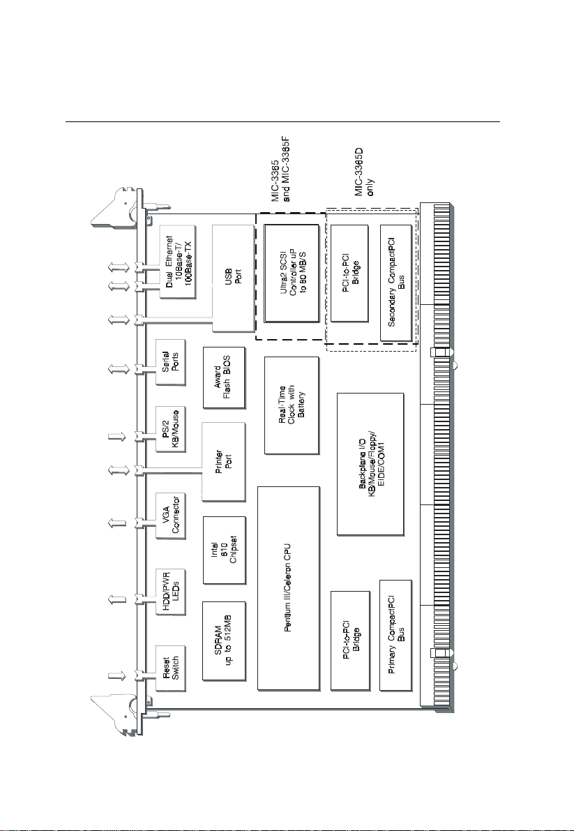
1.4 Function Block Diagram
Figure 1-1: MIC-3365 function block diagram
6 MIC-3365 User's Manual
Page 17
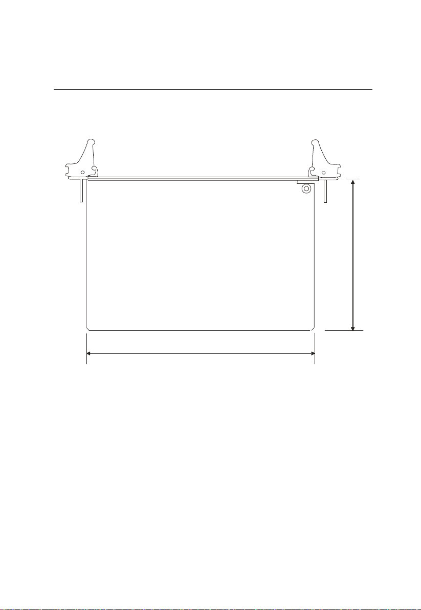
1.5 Board Dimensions
233.35 mm
160 mm
Figure 1-2: MIC-3365 board dimensions
Chapter 1 Hardware Configuration 7
Page 18
1.6 Jumpers
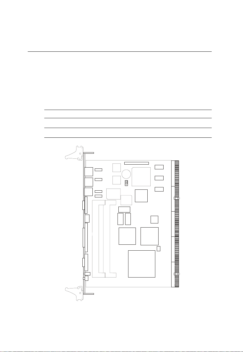
1.6.1 Jumper Locations
The MIC-3365 provides jumpers for configuring your board for
specific applications other than the default settings.
Table 1-1 list the jumper functions. Figure 1-3 illustrates the jumper
locations. The default jumper setting is illustrated in Figure 1-3.
Table 1-1: MIC-3365 jumper descriptions
Number Function
JP5 Clear CMOS
JP5
Figure 1-3: MIC-3365 jumper locations
8 MIC-3365 User's Manual
Page 19
1.6.2 Jumper Settings
This section tells how to set the jumpers to configure your card. It
gives the card default configuration and your options for each jumper.
After you set the jumpers and install the card, you will also need to
run the BIOS Setup program (discussed in Chapter 6) to configure the
serial port addresses, floppy/hard disk drive types and system
operating parameters. Connections, such as hard disk cables, appear
in Chapter 2.
For the locations of each jumper, see the board layout diagram
depicted earlier in this chapter.
You configure your card to match the needs of your application by
setting jumpers. A jumper is a metal bridge that closes an electrical
circuit. It consists of two metal pins and a small metal cap (often
protected by a plastic cover) that slides over the pins to connect them.
To "close" a jumper you connect the pins with the cap. To "open" a
jumper you remove the cap. Sometimes a jumper will have three pins,
labeled 1, 2 and 3. In this case you connect either pins 1 and 2 or 2
and 3.
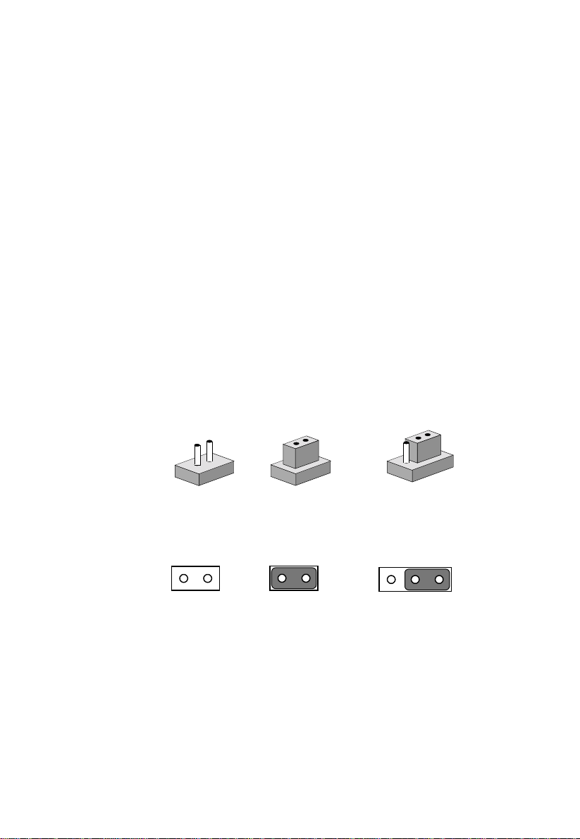
Open Closed Closed 2-3
3
2
1
The jumper settings are schematically depicted in this manual as
follows:
1
Open Closed Closed 2-3
You may find a pair of needle-nose pliers useful for setting the
jumpers.
If you have any doubts about the best hardware configuration for
your application, contact your local distributor or sales representative
before you make any changes.
Chapter 1 Hardware Configuration 9
Page 20

1.6.3 Clear CMOS (JP5)
This jumper is used to erase CMOS data and reset system BIOS
information. Follow the procedures below to clear the CMOS.
1. T urn of f the system.
2. Close jumper JP5 (2-3) for about 2-3 seconds.
3. Close jumper JP5 (1-2).
4. Turn on the system. The BIOS is reset to its default setting.
Table 1-2: Clear CMOS
CMOS JP5
Clear
321
Normal
10 MIC-3365 User's Manual
321
Page 21

1.7 Connectors
On-board connectors link to external devices such as hard disk drives,
keyboards, or floppy drives, etc. Table 1-3 lists the function of each
connector and Figure 1-4 and Figure 1-5 illustrate each connector
location. Chapter 2 gives instructions for connecting external
devices to your card.
Table 1-3: MIC-3365 connector descriptions
Number Function
CN3 Reset switch
CN 1 Parallel port
CN2 VGA connector
LED2 HDD LED and Power LED
CN 4 Ethernet connector 1
CN 5 Ethernet connector 2
CN6 COM2
CN 7 PS/2 Keyboard and mouse connector
CN 8 USB connector
CN10 Fan connector
CN11 Floppy disk drive connector
CN12 IDE connector
CN13 COM1
DIM1 DIMM socket 1
DIM2 DIMM socket 2
J1/J2 Primary CompactPCITM bus
J3/J4/J5 Rear I/O transition
CPU1 Socket 370 for CPU
Please refer to Appendix B for pin assignments.
Chapter 1 Hardware Configuration 11
Page 22
Figure 1-4: MIC-3365 connector locations
12 MIC-3365 User's Manual
Page 23
1.8 Front Panel Connectors and Indicators
LAN1
LAN2
USB
COM1
PRINTER
VGA
PWRHDD
RESET
TM
LAN1
LAN2
USB
COM1
PRINTER
VGA
HDD
RESET
RESET
PWRHDD
TM
TM
LAN1
LAN2
USB
COM1 COM2
PRINTER
VGA
PWR
FDD
MIC-3365 MIC-3365D
MIC-3365F
Figure 1-5: MIC-3365 front panel connector and indicator locations
Chapter 1 Hardware Configuration 13
Page 24

1.9 Installing SDRAM (DIMMs)
The MIC-3365 provides two 168-pin DIMM sockets. Each socket
accepts either 16, 32, 64, 128 or 256 MB SDRAM. The sockets can
be filled in any combination with DIMMs of any size, giving a total
memory capacity between 16 and 512 MB.
Since the MIC-3365 can operate at 66 or 100 MHz, we recommend
using PC100-compliant DIMMs.
The procedure for installing DIMMs appears below. Please follow
these steps carefully.
1. Ensure that all power supplies to the system are switched Off.
2. Install the DIMM modules. Install the DIMM so that its gold pins
point down into the DIMM socket.
3. Slip the DIMM into the socket and carefully fit the bottom of the
card against the connectors.
4. Gently push the DIMM into the socket, until the clips on the ends
of the DIMM sockets snap into place.
5. Check to ensure that the DIMM is correctly seated and all connector contacts touch. The DIMM should not move around in its
socket.
Note: The DIMM modules can only fit into sockets one way ,
in accordance with the keyed notches along the
bottom edge of the modules. Their gold pins must
point down into the DIMM socket.
14 MIC-3365 User's Manual
Page 25

Note: To ensure compatibility between the MIC-3365 and
DRAMmodules, our R&D team has compiled a list of
recommended SDRAMs. Only those which have
passed the team’s strict and rigorous testing procedures are included. Please refer to the table below.
You may order the SDRAMs locally or from Advantech. If you want to buy from us, please contact
Advantech’s sales representatives for details.
rodneV
ataD
ataD
neginU5633U1590T
neginU5633U2590T
gniredrO
rebmuN
CEN
seitlaicepS
seitlaicepS
5633F1590T
CEN
5633F2590T
CEN
CEN
emaNpihCyticapaCnoitacificepS
08A-5G3614654D
01A-5G3614654D
08A-5G36182154D
01A-5G36182154D
08A-5G3614654D
01A-5G3614654D
08A-5G36182154D
01A-5G36182154D
BM46001-CP
BM821001-CP
BM46001-CP
BM821001-CP
Table 1-4: Recommended SDRAM
Chapter 1 Hardware Configuration 15
Page 26
1.10 Installing CPU heat sink and HDD, FDD brackets
The MIC-3365 accepts Intel® socket 370 Pentium® III Cuppermine
CPU or Intel® socket 370 CeleronTM CPU. In order to meet critical
environmental conditions and the physical space of the MIC-3365 at
the same time, Advantech designed a heat sink to fulfill both needs.
Please refer to Figure 1-6 for an illustration of the heat sink used for
the MIC-3365 and MIC-3365D, 1-slot wide solution. Figure 1-7
illustrates the installation method of the heat sink, HDD, and FDD
brackets used for the MIC-3365F.
Because the thickness of the Pentium® III and CeleronTM CPU are
different, Advantech provides a samll aluminum plate along with the
heat sink when installed with a Pentium® III CPU. The small aluminum plate is default fastened on the heat sink in the factory. If users
would like to use a CeleronTM CPU on the MIC-3365, please remove
the small aluminum plate from the heat sink.
Figure 1-6: Heat sink installation for 1 slot wide solution
16 MIC-3365 User's Manual
Page 27
Figure 1-7: Heat sink installation for 2 slot wide solution
Chapter 1 Hardware Configuration 17
Page 28

1.11 Software Support
The MIC-3365 supports lots of operating systems, such as Microsoft
Windo ws family , Linux, SCO UNIX, QNX, etc.
Note: At the beginning of QNX installation process, please
follow the system's installation guide shown on the
screen. Press anykey and F2 when asked, and then
choose VGA 16 Color Only , and press <space> to
continue. Otherwise, you won't be able to contiune
installing QNX.
18 MIC-3365 User's Manual
Page 29

Connecting
Peripherals
2
CHAPTER
Page 30

2.1 IDE Device (CN12)
The MIC-3365 provides two IDE (Integrated Device Electronics)
channels via the J3 connector to the rear transition board MIC-3302.
Four IDE drives can be connected to the MIC-3365 through the rear
transition board MIC-3302.
The MIC-3365F provides a mounting bracket to mount a 2.5" hard
disk drive on board. Users can connect this 2.5" hard disk drive to the
on-board 44-pin IDE connector (CN12).
Users can connect two IDE drives to each IDE channel. If two drives
are installed on one channel, remember to set one as the master and
the other one as the slave. You may do this by setting the jumpers on
the drives. Refer to the documentation that came with your drive for
more information. A jumper diagram usually appears on the top side
of a hard disk drive.
Warning: Plug the other end of the cable into the drive with pin
1 on the cable corresponding to pin 1 on the drive.
Improper connection will damage the drive.
Note: We don't recommend connection to the following
Seagate brand IDE HDD models: ST 31276A, ST
31720A, ST 32531A, ST 33240A or ST 34340A
2.2 Floppy Drive (CN11)
The MIC-3365 supports two floppy disk drives via the J3 connector
to the rear transition board MIC-3302. Users can connect up to two
floppy drives to the connector on the MIC-3302.
The MIC-3365F provides a mounting bracket to mount a slim-type
floppy disk drive on board. Users can connect this slim-type FDD to
the CN11 connector.
20 MIC-3365 User's Manual
Page 31

2.3 VGA Display Connector (CN2)
The MIC-3365 provides an VGA chipset built-in display for high
performance application. The MIC-3365's CN2 is a DB-15 connector
for V GA monitor input. Pin assignments for the VGA display are
detailed in Appendix A.
2.4 Parallel Port Connector (CN1)
The parallel port is normally used to connect the CPU board to a
printer. The MIC-3365 includes an on-board parallel port, accessed
through a DB 25-pin connector, CN1, on the front panel.
The parallel port is designated as LPT1 and can be disabled or
changed to LPT2 or LPT3 from the system BIOS setup.
2. 5 PS/2 Keyboard and Mouse Connector (CN7)
The MIC-3365 provides a 6-pin mini-DIN connector (CN7) on the
front panel for connection of PS/2 keyboard and PS/2 mouse. The
MIC-3365 comes with a cable to convert from the single 6-pin miniDIN connector to a double PS/2 keyboard connector and PS/2 mouse
connector. Since these two connectors are identical, please follow the
icons on the cable to plug the keyboard and the mouse into their
correct connectors.
2. 6 Serial Ports (CN13 and CN6)
The MIC-3365 offers two serial ports: COM1 and COM2 in
MIC-3365F version, both in RS-232. These ports allow users to
connect to serial devices (a mouse, printers, etc.) or a communication
network.
You can select the address for each port ( For example, 3F8H [COM1],
2F8H [COM2]) or disable it, using the BIOS Adv anced Setup program, covered in Chapter 6.
Different devices implement the RS-232 standard in different ways. If
you are having problems with a serial device, be sure to check the pin
assignments for the connector.
Chapter 2 Connecting Peripherals 21
Page 32

The IRQ and address range for both ports are fixed. However, if you
wish to disable the port or change these parameters later, you can do
this in the system BIOS setup. The table below shows the settings for
the MIC-3365 board's ports:
Table 2-1: MIC-3365 serial port default settings
Port Address Default
COM1 3F8, 3E8 3F8/IRQ4
COM2 2F8, 2E8 2F8/IRQ3
2.7 Ethernet Configuration (CN4 and CN5)
The MIC-3365 is equipped with dual high performance 32-bit PCIbus Fast Ethernet interfaces which are fully compliant with IEEE
802.3u 10/100Base-TX specifications. It is supported by all major
network operating systems and is 100% Novell NE-2000 compatible.
Two on-board RJ-45 jacks provide convenient connection to the
network.
The medium type can be configured via the software program
included on the utility CD-ROM disc. (See Chapter 3 for detailed
information.)
2.8 USB Connector (CN8)
The MIC-3365 provides one USB (Universal Serial Bus) interface on
the front panel, and the MIC-3365F provides two USB interfaces on
the front panel. The USB interface gives complete plug and play, hot
attach/detach for up to 127 external devices. The MIC-3365 USB
interfaces comply with USB specification rev. 1.0 and are fuse
protected.
The USB interfaces can be disabled in the system BIOS setup. The
USB controller default is "Enabled" but the USB keyboard support
default is "Disabled".
22 MIC-3365 User's Manual
Page 33

2. 9 Ultra 2 SCSI Interface
The MIC-3365 and MIC-3365F provides an Ultra 2 SCSI interface on
the rear transition board MIC-3302 via the J5 connector. The
MIC-3302 has a 68-pin, dual in-line connector for Ultra 2 SCSI
devices. Connection of SCSI devices requires special attention,
especially when determining the last drive on the SCSI chain. Refer
to Chapter 5 and your device's operating manual for detailed installation advice.
2.10 Card Installation
The CompactPCI connectors are firm and rigid, and require careful
handling while plugging and unplugging. Improper installation of a
card can easily damage the backplane of the chassis.
The inject/eject handles of MIC-3365 help you install and remove
the card easily and safely. Follow the procedure below to install the
MIC-3365 into a chassis:
To install a card:
1. Hold the card vertically. Be sure that the card is pointing in the
correct direction. The components of the card should be pointing
to the right-hand side.
2. Holding both handles, pull out the red portion in the middle of the
handle to unlock it.
Caution: Keep your fingers away from the hinge to prevent your
fingers from getting pinched.
3. Insert the card into the chassis by sliding the upper and lower
edges of the card into the card guides.
4. Push the card into the slot gently by sliding the card along the card
guide until the handles meet the rectangular holes of the cross
rails.
Note: If the card is correctly positioned and has been slid
all the way into the chassis, the handle should match
the rectangular holes. If not, remove the card from
Chapter 2 Connecting Peripherals 23
Page 34
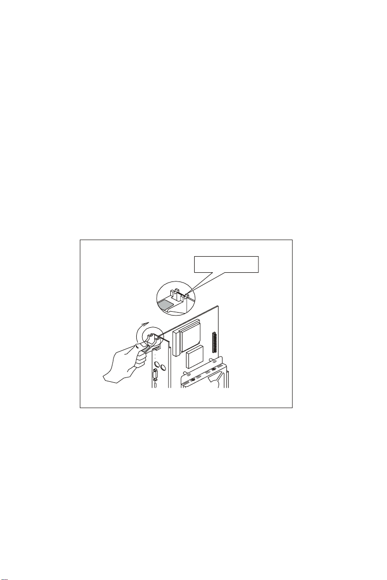
the card guide and repeat step 3 again. Do not try to
install a card by forcing it into the chassis.
5. Pull the upper handle down and lift the lower handle up to push
the card into place.
6. Secure the card by pushing in the red handle to lock it into place.
To remove a card:
1. Unscrew the screws on the front panel. Pull out the red portion in
the middle of the handle to unlock the handle.
2. Lift the upper handle up and press the lower handle down to
release the card from the backplane.
3. Slide the card out.
Keep your fingers
away from this area.
Figure 2-1: Installing the card into the chassis
24 MIC-3365 User's Manual
Page 35

3
CHAPTER
Ethernet Software
Configuration
Page 36

3.1 Introduction
The MIC-3365 has two on-board high-performance fast Ethernet
interfaces which comply with IEEE 802.3/802.3u for 10Base-T and 100
Base-TX data rates.
The module uses two Intel® 82559 fast Ethernet controllers with
integrated PHY and is compatible with the Intel® PRO/100+ Server and
Client Adapter. The dual Ethernet channel design provides several
options for increasing throughput and fault tolerance when running
Windows NT 4.0 or NetWare 4.1x and newer versions of these,
includes:
•Adapter Fault Tolerance (AFT) - provides automatic redundancy for
your Ethernet channel. If the primary channel fails, the secondary
takes over.
• Adaptive Load Balancing (ALB) - creates a team of 2 channels to
increase transmission throughput. Also includes AFT and ALB.
This function works with any 100BASE-TX switch.
• Fast EtherChannel (FEC) - creates a team of 2 to 4 channels to
increase transmission and reception throughput. Also includes AFT.
This function requires a Cisco switch with FEC capability.
The MIC-3365 comes with drivers for a wide variety of networks and
operating systems. The MIC-3365 is an excellent choice for operation
in standalone and harsh industrial environments.
3.2 Utility and Drivers
The MIC-3365's on-board Ethernet interface supports all major network
operating systems. The installation instructions and drivers for
different operating systems are located in the following directories of
the utility CD-ROM disc:
General Information:
• \MIC3365\LAN\README.TXT: General information about the
drivers
For Microsoft Windows:
• \MIC3365\LAN\INFO\MS\MS.TXT: Installation instructions for
26 MIC-3365 User's Manual
Page 37

Microsoft Windows
• \MIC3365\LAN\E100BNT.SYS (NDIS 4.0), \MIC3365\LAN\
OEMSETUP .INF: Drivers for Windows NT 4.0
• \MIC3365\LAN\E100B.SYS (NDIS 3), \MIC3365\LAN\
OEMSETUP .INF: Drivers for Windows NT 3.51
• \MIC3365\LAN\NET82557.INF: Drivers for Windows 98
• \MIC3365\LAN\E100BNT.SYS (NDIS 4.0), \MIC3365\LAN\
NET82557.INF: Drivers for Windows 95
• MIC3365\LAN\WFW\E100B.38_, \MIC3365\LAN\WFW\
OEMSETUP.INF: Drivers for W indows 3.1
For Novell NetWar e
• \MIC3365\LAN\INFO\NETWARE\NETW ARE.TXT: Installation
instructions for Novell NetW are
• \MIC3365\LAN\NWSERVER\3X4X.OLD\E100B.LAN: Drivers for
NetW are 3.12 and 4.10
• \MIC3365\LAN\NWSER VER\311LAN\E100B.LAN: Drivers for
NetW are 3.11
• \MIC3365\LAN\OS2\E100BODI.SYS: Drivers for NetWare OS/2
ODI Client
• \MIC3365\LAN\DOS\E100BODI.COM: Drivers for DOS ODI Client
For UNIX
• \MIC3365\LAN\INFO\UNIX\UNIX.TXT: Installation instructions for
UNIX
For Other Operating Systems
• \MIC3365\LAN\INFO\OTHER\OTHER.TXT: Installation instructions for other operating systems
• \MIC3365\LAN\DOS\E100B.DOS: Drivers for IBM LAN support
for AS/400 and NetW are (for LANSUP)
• \MIC3365\LAN\DOS\E100BODI.COM: Drivers for IBM LAN
Chapter 3 Ethernet Software Configuration 27
Page 38

support for AS/400 and NetW are (for ODINSUP)
• \MIC3365\LAN\OS2\E100B.OS2: Drivers for LAN server
(OS/2 driver)
• \MIC3365\LAN\DOS\E100B.DOS: Drivers for LAN server
(DOS driver)
• \MIC3365\LAN\DOS\E100B.DOS: Drivers for BANY AN NDIS
workstation
• \MIC3365\LAN\DOS\E100B.DOS: Drivers for LANT ASTIC 6.0
• \MIC3365\LAN\DOS\E100B.DOS: Drivers for general NDIS 2.X
(DOS driver)
• \MIC3365\LAN\OS2\E100B.OS2: Drivers for general NDIS 2.X
(OS/2 driver)
Before installing drivers, please refer to the installation instructions of each
operating system.
Note: Do not use the driver recommended by the Windows
95/98/NT Add New Hardware wizard. Choose the
driver from the utility CD-ROM disc.
Note: Operating system vendors may post driver updates
on their web sites. Please visit the web sites of OS
vendors to download updated drivers.
28 MIC-3365 User's Manual
Page 39

3.3 Installation for Windows NT 4.0
Before installing; create a new folder [!] ,\MIC3365\LAN\, in your
"E:" drive on your hard disk drive, and download all files from the
directory, \MIC3365\LAN\, on the utility CD-ROM to it.
1. In the Windows NT screen, select "Start", click "Settings".
Click the "Control Panel" item and choose "Network".
2. Click "Y es".
Chapter 3 Ethernet Software Configuration 29
Page 40
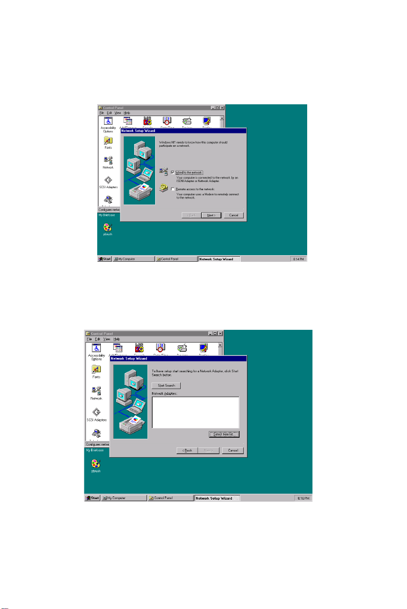
3. Click "Wired to the Network", or users may choose "Remote
access to the network" if applicable.
4. Click "Select from list".
30 MIC-3365 User's Manual
Page 41

5. Click "Have Disk".
6. T ype in "E:\MIC3365\LAN" in the blank column and click "OK".
Chapter 3 Ethernet Software Configuration 31
Page 42

7. Click "OK".
8. Click "Next".
32 MIC-3365 User's Manual
Page 43

9. Click "Next".
10. Click "Next".
Chapter 3 Ethernet Software Configuration 33
Page 44

11. Click "Next".
12. Insert Windows NT source disc in drive E. T ype "E:\I386" in
the blank column or any other directory that contains the
Windows NT files. Click "Continue".
34 MIC-3365 User's Manual
Page 45

13. W ait for the installation to finish.
14. Complete the settings with users' network settings. Click "OK".
Chapter 3 Ethernet Software Configuration 35
Page 46

15. Click "Next".
16. Click "Next".
36 MIC-3365 User's Manual
Page 47

17. Click "Yes" to restart the computer and enable the changes to
take effect.
Chapter 3 Ethernet Software Configuration 37
Page 48

38 MIC-3365 User's Manual
Page 49

4
CHAPTER
AGP VGA Setup
Page 50

4.1 Introduction
The MIC-3365 uses chipset built-in AGP VGA display . This chapter
describes how to install the VGA drivers to the MIC-3365.
4.2 Installation of SVGA Driver
The MIC-3365 is supplied with a utility CD-ROM disc that holds the
necessary files for setting up the VGA display under the directory
\MIC-3365\VGA. The contents and path names of this directory are
listed below:
• MIC3365\VGA\Win31 1: VGA utility for Windows 3.1
• MIC3365\VGA\Win9x: VGA utility for Windows 95/98
• MIC3000\VGA\Nt351: Utility for W indows NT 3.51
• MIC3365\VGA\Nt40: VGA utility for W indows 4.0
Complete the following steps to install the VGA driver. Follow the
procedures in the flow chart that apply to the operating system you
are using with your MIC-3365.
40 MIC-3365 User's Manual
Page 51
4. 3 Installation for Windows NT 4.0
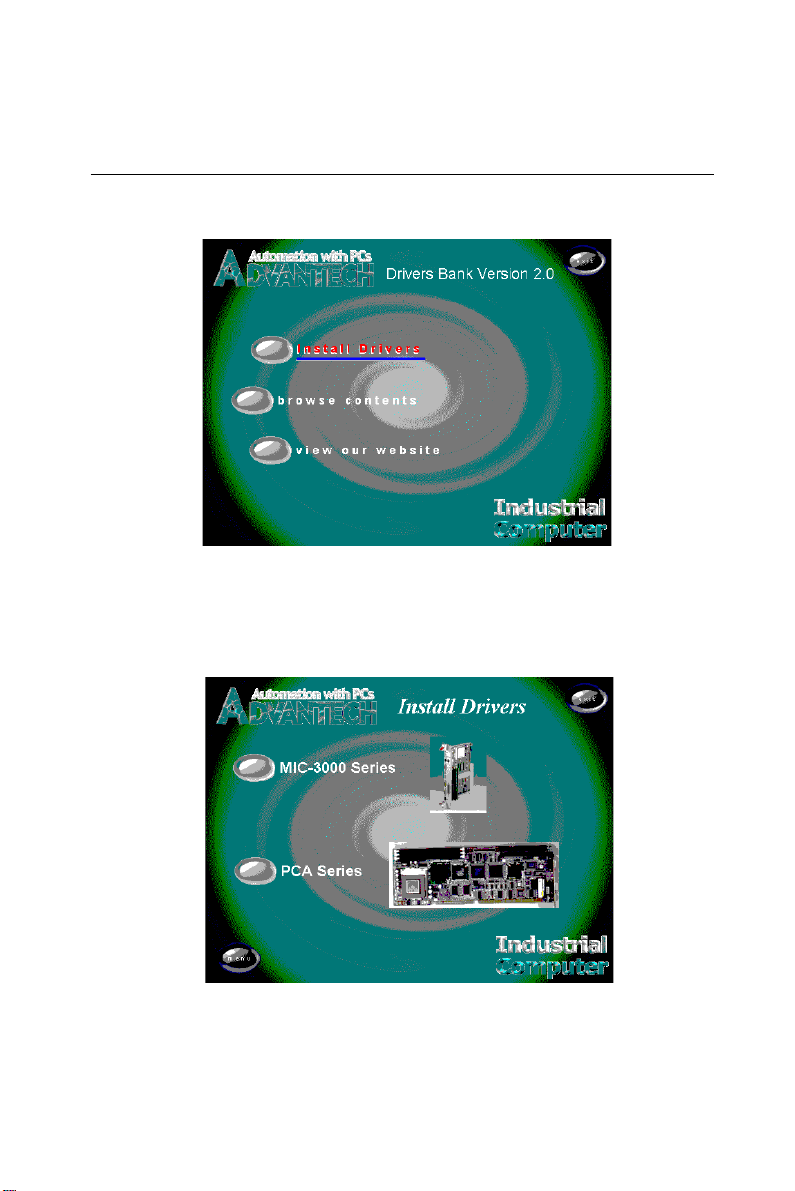
1. Insert the utility CD-ROM disc in the CD-ROM drive and wait for the
auto-run screen to pop up. Click "Install Drivers".
2. Click "MIC-3000 Series".
Chapter 4 AGP VGA Setup 41
Page 52
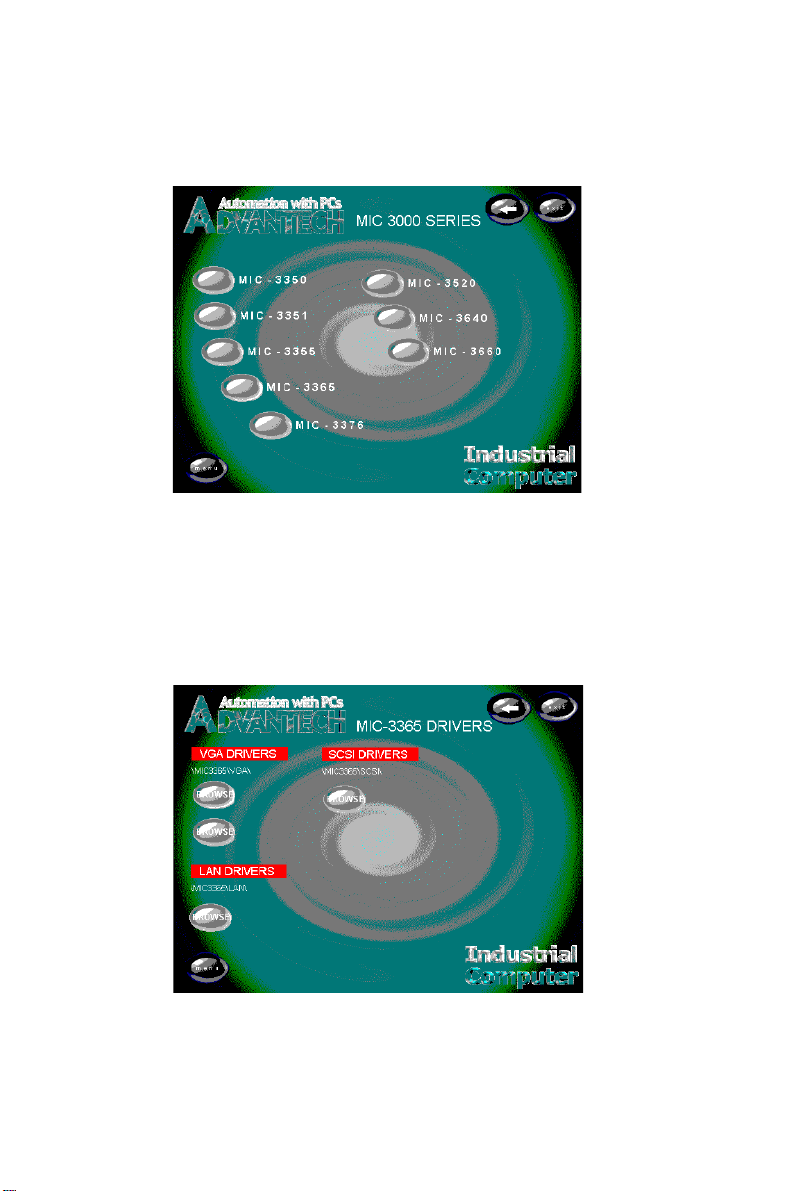
3. Click "MIC-3365".
4. Under VGA Drivers menu, click "Browse" to choose the operating
system used.
42 MIC-3365 User's Manual
Page 53
5. Click "Nt40".
6. Click "Graphics".
Chapter 4 AGP VGA Setup 43
Page 54
7. Click "Setup.exe".
8. Click "Next".
44 MIC-3365 User's Manual
Page 55

9. Click "Y es".
10. Click "Next" to install drivers.
Chapter 4 AGP VGA Setup 45
Page 56
11. W ait for installation to finish.
12. Click "Finish" to restart the computer and enable the changes to
take effect.
46 MIC-3365 User's Manual
Page 57

SCSI Software
Configuration
5
CHAPTER
Page 58

5.1 Introduction
The MIC-3365 uses the Symbios SYM53C895 SCSI processor to
provide an Ultra 2 SCSI interface on the rear transition board MIC-3302
via the J5 connector. The Ultra 2 SCSI interface has a data transfer rate
up to 80 MB/s. The device can support cables up to 12-meter long and
up to 16 L VD devices on a wide L VD ( Low Voltage Differential) SCSI
bus. Device drivers and utilities for DOS, Windows 95/98/NT , OS/2,
SCO UNIX, UnixW are and NetW are are included in the utility CD-ROM
disc.
5.2 Utility and Drivers
The utility user's guide and installation instructions are provided in the
utility CD-ROM disc. The instructions are located in the directory
\MIC3365\SCSI and include:
For DOS:
• \MIC3365\SCSI\DOS\DOS.TXT: Installation instructions for DOS
• \MIC3365\SCSI\DOS\INSTALL.EXE: Drivers for DOS
For Windows 95/98:
• \MIC3365\SCSI\WIN9X\WIN9598.TXT: Installation instructions
for Windows 95/98
• \MIC3365\SCSI\WIN9X\SYMC8XX.INF: Drivers for W indows 95/
98
For Windows NT :
• \MIC3365\SCSI\WINNT\WINNT.TXT: Installation instructions for
Windows NT 4.0
• \MIC3365\SCSI\WINNT\OEMSETUP.INF: Drivers for Windows NT
4.0
48 MIC-3365 User's Manual
Page 59

For OS/2:
• \MIC3365\SCSI\OS2\OS2.TXT: Installation instructions for OS2
• \MIC3365\SCSI\OS2\SYM8XXPC.EXE,
\MIC3365\SCSI\OS2\SYM_HIPC.EXE: Drivers for OS2
Note: The installation procedures below assume users' CD-
ROM drive name is E.
Chapter 5 SCSI Software Configuration 49
Page 60

5.3 Installation for Windows NT 4.0
1. In the Windows NT screen, select "Start", click "Settings".
Click the "Control Panel" item and choose "SCSI Adapters".
2. Click "Add".
50 MIC-3365 User's Manual
Page 61

3. Click "Have Disk".
4. Click "Browse".
Chapter 5 SCSI Software Configuration 51
Page 62

5. Click "Cancel".
6. Click "My Computer".
52 MIC-3365 User's Manual
Page 63

7. Click "Drv_Bank (E)".
8. Click "MIC3365".
Chapter 5 SCSI Software Configuration 53
Page 64

9. Click "SCSI".
10. Click "Winnt".
54 MIC-3365 User's Manual
Page 65
11. Click "Oemsetup".
12. Click "OK".
Chapter 5 SCSI Software Configuration 55
Page 66

13. Click "OK".
14. Click "Continue".
56 MIC-3365 User's Manual
Page 67

13. Click "Yes" to restart the computer and enable the changes to take
effect.
Chapter 5 SCSI Software Configuration 57
Page 68

58 MIC-3365 User's Manual
Page 69

6
CHAPTER
Award BIOS Setup
Page 70
6.1 Introduction
A ward's BIOS ROM has a built-in Setup program that allows users to
modify the basic system configuration. This type of information is
stored in battery-backed CMOS so that it retains the Setup information
when the power is turned off.
6.2 Entering Setup
Turn on the computer and check for the "patch code". If there is a
number assigned to the patch code, it means that the BIOS supports
your CPU.
If there is no number assigned to the patch code, please contact
Advantech's application engineer to obtain an up-to-date patch code
file. This will ensure that your CPU's system status is valid.
After ensuring that you have a number assigned to the patch code,
press <DEL> and you will immediately be allowed to enter Setup.
Figure 6-1: Initial Setup screen
60 MIC-3365 User's Manual
Page 71
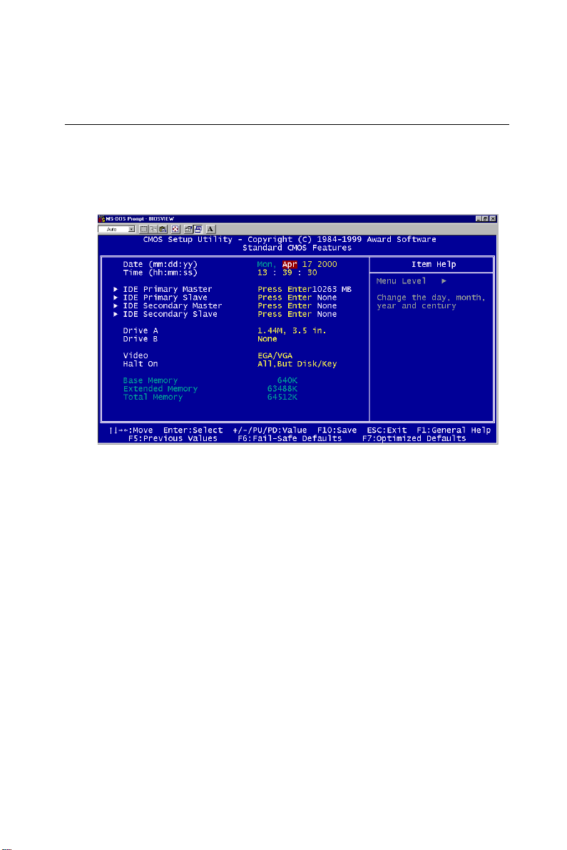
6.3 Standard CMOS Features
Choose the "ST ANDARD CMOS FEA TURES" option from the
INITIAL SETUP Menu, and the screen below will be displayed. This
standard setup menu allows users to configure system components
such as date, time, hard disk drive, floppy drive, display, and memory.
Figure 6-2: Standard CMOS Features screen
Chapter 6 Award BIOS Setup 61
Page 72
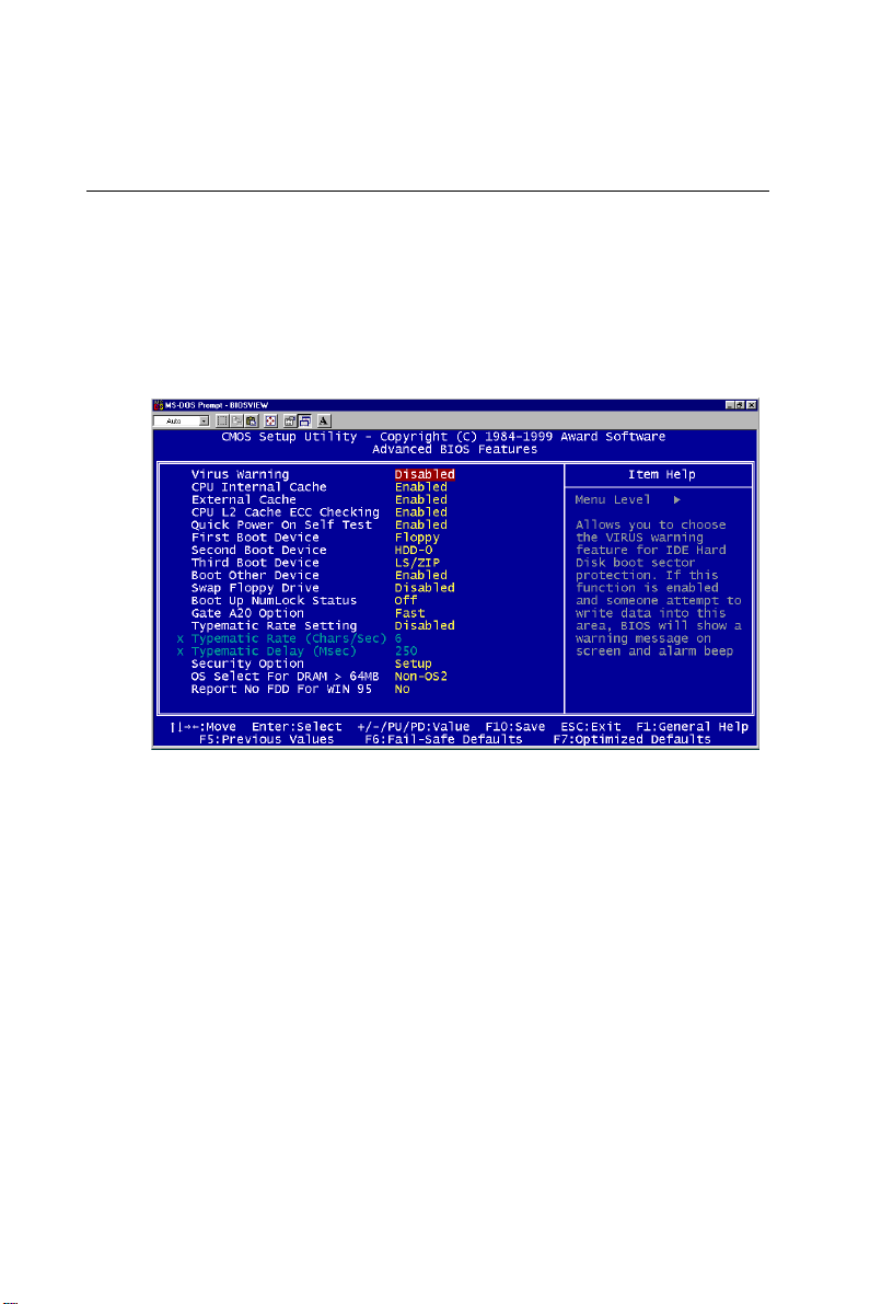
6.4 Advanced BIOS Features
The "ADVANCED BIOS FEA TURES" screen will appear after choosing the ADV ANCED BIOS FEATURES item from the INITIAL SETUP
Menu. This screen allows users to configure the MIC-3365 according
to their particular requirements.
Below are some major items that are provided in the ADV ANCED BIOS
FEA TURES screen:
Figure 6-3: Advanced BIOS Features screen
Virus Warning
During and after the system boots up, any attempt to write to the boot
sector or partition table of the hard disk drive will halt the system. If
this happens, a warning message will be displayed. You can run the
anti-virus program to locate the problem.
If Virus Warning is Disabled, no warning message will appear if
anything attempts to access the boot sector or hard disk partition.
CPU Internal Cache/External Cache
Depending on the CPU/chipset design, these options can speed up
memory access when enabled.
62 MIC-3365 User's Manual
Page 73

CPU L2 Cache ECC Checking
This option controls the ECC capability in the CPU level 2 cache.
Quick Power On Self Test
This option speeds up the Power-On Self Test (POST) conducted as
soon as the computer is turned on. When enabled, the BIOS shortens
or skips some of the items during the test. When disabled, normal
POST procedures resume.
First/Second/Third Boot Devices
These options determines the boot up sequence. The default value for
the first, second, and third devices options are "Floppy, HDD-0, and
LS/ZIP" respectively. The following options are available:
Floppy: Computer will boot from the floppy disk drive
LS/ZIP: Computer will boot from the LS or ZIP drive
HDD-0: Computer will boot from the primary master hard disc drive
SCSI: Computer will boot from the SCSI drive
CD-ROM: Computer will boot from the CD-ROM drive
HDD-1: Computer will boot from the primary slave hard disk drive
HDD-2: Computer will boot from the secondary master hard disk drive
HDD-3: Computer will boot from the secondary slave hard disk drive
Dis ab le d : Computer will boot from other devices such as DOC 2000 or
CompactFlash
Boot Other Devices
This option allows users to boot from other connected devices such
as DOC 2000 or CompactFlash
®
Swap Floppy Drive
If the system has two floppy disk drives, choose enable to assign
physical drive B to logical drive A, and vice versa.
Gate A20 option
Normal The A20 signal is controlled by the keyboard controller
or chipset hardware
Fast Default: Fast. The A20 signal is controlled by Port 92 or
by a specific chipset method.
Chapter 6 Award BIOS Setup 63
Page 74

Typematic Rate Setting
The typematic rate determines the characters per second accepted by
the computer. Typematic Rate setting enables or disables the typematic
rate.
Typematic Rate (Char/Sec)
BIOS accepts the following input values (character/second) for
Typematic Rate: 6, 8, 10, 12, 15, 20, 24, 30.
Typematic Delay (msec)
When holding down a key , the T ypematic Delay is the time interval
between the appearance of the first and second characters. The input
values (msec) for this category are: 250, 500, 750, 1000.
Security Option
This setting determines whether the system will boot if the password
is denied, while limiting access to Setup.
System The system will not boot, and access to Setup will be
denied if the correct password is not entered at the
prompt.
Setup The system will boot, but access to Setup will be
denied if the correct password is not entered at the
prompt.
Note: To disable security, select SET PASSWORD in the
INITIAL SETUP menu. At this point, you will be
asked to enter a password. Simply hit the <ENTER>
key to disable security. When security is disabled,
the system will boot, and you can enter Setup freely .
OS Select for DRAM>64 MB
This setting is for use under the OS/2 operating system.
Report No FDD For WIN 95
This option allows the MIC-3365 to report a warning message if the
system detected no FDD in Windows 95 environment.
64 MIC-3365 User's Manual
Page 75

6.5 CHIPSET Features Setup
Choose the "ADV ANCED CHIPSET FEATURES" option from the
INITIAL SETUP Menu, and the screen below will be displayed. This
sample screen contains the manufacturer's default values for the
MIC-3365.
6.6 Integrated Peripherals
Figure 6-4: Advanced Chipset Features screen
Chapter 6 Award BIOS Setup 65
Page 76

6.7 Power Management Setup
The power management setup controls the CPU cards' "green"
features. The following screen shows the manufacturer's default
values.
Figure 6-5: Integrated Peripherals screen
Note: If you enable the IDE HDD block mode, the en-
hanced IDE driver will be enabled.
66 MIC-3365 User's Manual
Page 77

6.8 PnP/PCI Configurations
Figure 6-6: Power Management Setup screen
Power Management
This option allows you to determine if the values in power management are disabled, user-defined, or predefined.
HDD Power Management
You can choose to turn the HDD off after one of the time intervals
listed, or when the system is in Suspend mode. If in a power saving
mode, any access to the HDD will wake it up.
Note: The HDD will not power down if the Power Manage-
ment option is disabled.
Chapter 6 Award BIOS Setup 67
Page 78

6.9 Load Optimized Defaults
"LOAD OPTIMIZED DEF AUL TS" loads the most appropriate values
of the system parameters for maximum performance.
Figure 6-7: PnP/PCI Configurations screen
Figure 6-8: Load Optimized Defaults screen
68 MIC-3365 User's Manual
Page 79

6.10 Set Password
T o change, confirm, or disable the password, choose the "SET
P ASSWORD" option from the INITIAL SETUP menu, and press
[Enter]. The password can be at most 8 characters long.
Remember to enable this feature. Y ou must first select the "SECURITY
OPTION" in the ADV ANCED BIOS FEATURES to be either "Setup" or
"System." Pressing [Enter] again without typing any characters can
disable the password setting function.
Figure 6-9: Set Password screen
Chapter 6 Award BIOS Setup 69
Page 80
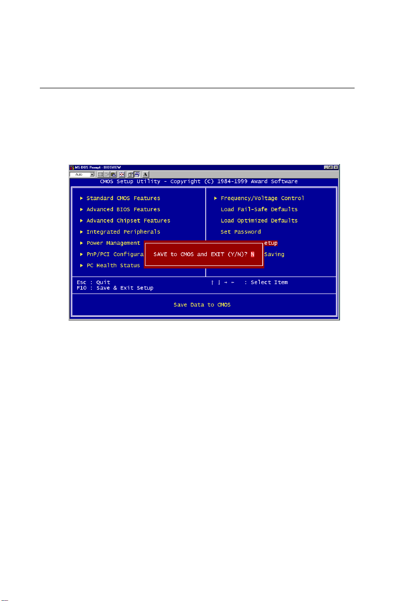
6.11 Save & Exit Setup
If you select this and press the [Enter] key, the values entered in the
setup utilities will be recorded in the CMOS memory of the chipset.
The microprocessor will check this every time you turn your system on
and compare this to what it finds as it checks the system. This record
is required for the system to operate.
Figure 6-10: Save & Exit Setup screen
70 MIC-3365 User's Manual
Page 81

6.12 Exit Without Saving
Selecting this option and pressing the [Enter] key lets you exit the
Setup program without recording any new values or changing old
ones.
Figure 6-11: Exit W ithout Saving screen
Chapter 6 Award BIOS Setup 71
Page 82

72 MIC-3365 User's Manual
Page 83

APPENDIX
A
Programming the
Watchdog Timer
Page 84

A.1 Programming the Watchdog Timer
T o program the watchdog timer, you must write a program which writes
a value to I/O port address 444 (hex). This output value represents time
interval. The value range is from 01 (hex) to 3F (hex), and the related
time interval is 1 sec. to 63 sec.
Data Time Interval
01 1 sec.
02 2 sec.
03 3 sec.
04 4 sec.
••
••
••
3 F 63 sec.
74 MIC-3365 User's Manual
Page 85

After data entry , your program must refresh the watchdog timer by
rewriting the I/O port 444 (hex) while simultaneously setting it. When
you want to disable the watchdog timer, your program should read I/O
port 444 (hex).
The following example shows how you might program the watchdog
timer in BASIC:
10 REM Watchdog timer example program
20 OUT &H443, data REM Start and restart the watchdog
30 GOSUB 1000 REM Your application task #1,
40 OUT &H443, data REM Reset the timer
50 GOSUB 2000 REM Your application task #2,
60 OUT &H443, data REM Reset the timer
70 X=INP (&H443) REM, Disable the watchdog timer
80 END
1000 REM Subroutine #1, your application task
••
••
••
1070 RETURN
2000 REM Subroutine #2, your application task
••
••
••
2090 RETURN
Appendix A Programming the Watchdog Timer 75
Page 86

76 MIC-3365 User's Manual
Page 87

B
APPENDIX
Pin Assignments
Page 88

B.1 VGA Display Connector (CN2)
1
6
11
5
10
15
Table B-1: MIC-3365 CRT display connector
Pin Signal Pin Signal
1 RED 9 VGAVCC
2 GREEN 10 GN D
3 BLUE 11 N/C
4 N/C 1 2 SDA
5 GND 13 HSYNC
6 GND 14 VSYNC
7 GND 15 SC L
8 GND
B.2 Keyboard and Mouse Connnector (CN7)
6
4
Table B-2: MIC-3365 keyboard connector
Pin Signal
1 KDAT
2 MDAT
3 GND
4 VCC
5 KCLK
6 MCLK
5
3
1
78 MIC-3365 User's Manual
Page 89

B.3 COM1 and COM2 Serial Port (CN13 and
1
5
9
6
CN6)
5
4
3
2
1
Table B-3: MIC-3365 COM1 and COM2 serial port
9
8
7
6
COM1 COM2
Pin Signal Pin Signal
1 NRLSD1 1 NRLSD2
2 NRX1 2 NRX2
3 NTX1 3 NTX2
4 NDTR1 4 NDTR2
5 GND 5 GND
6 NDSR1 6 NDSR2
7 NRTS1 7 NRTS2
8 NCTS1 8 NCTS2
9 NRI1 9 NRI2
Appendix B Pin Assignments 79
Page 90

B.4 USB Connector (CN8)
1 4
USB2
USB1
Table B-4: MIC-3365 USB1/USB2 connector
USB1 USB2
Pin Signal Pin Signal
1 VCC 1 VCC
2 USBD0- 2 USBD13 USBD0+ 3 USBD1+
4 GND 4 GND
B.5 Ethernet RJ-45 Connector (CN4 and CN5)
Table B-5: MIC-3365 Ethernet RJ-45 connector
Pin Signal
1 TX+
2 TX3 RX+
4N/C
5N/C
6 RX7N/C
8N/C
80 MIC-3365 User's Manual
Page 91

B.6 Parallel Port Connector (CN1)
13
25 14
Table B-6: MIC-3365 parallel port connector
Pin Signal
1 STB#
2 PTD0
3 PTD1
4 PTD2
5 PTD3
6 PTD4
7 PTD5
8 PTD6
9 PTD7
10 ACK#
11 BUSY
12 PE
13 SLCT
14 AFD#
15 ERR#
16 INIT#
17 SLIN#
18 GND
19 GND
20 GND
21 GND
22 GND
23 GND
24 GND
25 GND
1
Appendix B Pin Assignments 81
Page 92

B.7 IDE Connector (CN12)
43 41 .... 3 1
44 42 .... 4 2
Table B-7: MIC-3365 IDE connector
Pin Signal Pin Signal
1 IDE RESET# 2 G N D
3DATA 7 4DATA 8
5DATA 6 6DATA 9
7DATA 5 8DATA 10
9 DATA 4 10 DATA 11
11 DATA 3 12 DATA 12
13 DATA 2 14 DATA 13
15 DATA 1 16 DATA 14
17 DATA 0 18 DATA 15
19 GND 20 N/C
21 N/C 22 GND
23 IO WRITE# 24 GND
25 IO READ# 26 GND
27 IO CHANNEL READY 28 N/C
29 HDACK# 30 GND
31 IRQ14 3 2 N/C
33 ADDR 1 34 P66DET
35 ADDR 0 36 ADDR 2
37 HARD DISK SELECT 0# 38 HARD DISK SELECT 1#
39 IDE ACTIVE# 40 GND
41 VCC 42 VCC
43 GND 44 N/C
# low active
Note: The MIC-3665 supports DMA/66 HDD.
82 MIC-3365 User's Manual
Page 93

B.8 Floppy Drive Connnector (CN11)
1 2 .... 25 26
Table B-8: MIC-3351 floppy drive connector
Pin Signal Pin Signal
1 VCC 2 INDEX#
3 VCC 4 DSA#
5 VCC 6 DSKCHG
7N/C 8N/C
9 N/C 10 MOA#
11 N/C 12 DIR#
13 DEVSEL# 14 STEP#
15 GND 16 WDATA#
17 GND 18 WGATE#
19 GN D 20 TRAK0#
21 GND 22 WPT#
23 GND 24 RDATA#
25 G ND 26 HEAD#
# low active
Appendix B Pin Assignments 83
Page 94

B.9 System I/O Ports
Table B-9: System I/O ports
Addr. range (Hex) Device
000 - 00F DMA controller
020 - 021 Interrupt controller
040 - 043 8254 timer
060 IBM Enhanced keyboard
061 Speaker
070 -0 71 Real-time clock
081 - 083 DMA controller
087 DMA controller
089 - 08B DMA controller
08F - 091 DMA controller
0A0 - 0A1 Interrupt controller
0C0 - 0F0 DMA controller
0F0 - 0FF Math coprocessor
170 - 177 IDE controller
1F0 - 1F7 IDE controller
2F8 - 2FF UM 2
376 IDE controller
378 - 37A LPT1
3B0 - 3BB VGA adapter
3C0 - 3DF VGA adapter
3F0 - 3F5 FDD controller
3F6 IDE controller
3F7 FDD controller
3F8 - 3FF Serial port 1
480 - 48F PCI bus
4D0 - 4D1 PCI bus
778 - 77F ELP printer port
CF8 - CFF PCI bus
4000 - 40F7 PCI bus
5000 - 501F PCI bus
C000 - CFFF PCI-to-PCI bridge
D000 - D01E USB controller
F000 - F00E IDE controller
84 MIC-3365 User's Manual
Page 95

B.10 DMA Channel Assignments
Table B-10: DMA channel assignments
Channel Function
0 Available
1 Available
2 Floppy disk (8-bit transfer)
3 LPT1
4 Cascade for DMA controller 1
5 Available
6 Available
7 Available
B.11 Interrupt Assignments
Table B-11: Interrupt assignments
Interrupt# Interrupt source
IRQ 0 Interval timer
IRQ 1 Keyboard
IRQ 2 Interrupt from controller 2 (cascade)
IRQ 8 Real-time clock
IRQ 9 Cascaded to INT 0A (IRQ 2)
IRQ 10 Available
IRQ 11 Available
IRQ 12 PS/2 mouse
IRQ 13 INT from co-processor
IRQ 14 Fixed disk controller
IRQ 15 Available
IRQ 3 Serial communication port 2
IRQ 4 Serial communication port 1
IRQ 5 Available
IRQ 6 Diskette controller (FDC)
IRQ 7 Parallel port 1 (print port)
Appendix B Pin Assignments 85
Page 96

B.12 1st MB Memory Map
Table B-12: 1st MB memory map
Addr. range (Hex) Device
F000h - FFFFh System ROM
CC00h - EFFFh Unused
CA00h - CBFFh Used
C000h - C7FFh Expansion ROM
B800h - BFFFh CGA/EGA/VGA text
B000h - B7FFh Unused
A000h - AFFFh EGA/VGA graphics
0000h - 9FFFh Base memory
86 MIC-3365 User's Manual
Page 97

B.13 J1 connector pin assignments
Table B-13: J1 connector pin assignments
Pin Row A Row B Row C Row D Row E
25 +5V REQ64# ENUM# N/C +5V
24 AD1 +5 V N/C A D0 ACK64#
23 N/C AD4 AD3 +5V AD2
22 AD7 GND N/C AD6 AD5
21 N/C A D9 AD8 GND C/BE0#
20 AD12 GND N/C AD11 AD10
19 N/C AD15 AD14 GND AD13
18 SERR# GND N/C PAR C/BE1#
17 N/C SDONE SBO# GND PERR#
16 DEVSEL# GND N/C STOP# LOCK#
15 N/C FRAME# IRDY# GND TRDY#
14
13 KEY AREA
12
11 AD18 AD17 AD16 GND C/BE2#
10 AD21 GND N/C AD20 AD19
9 C/BE3# N/C AD23 GND AD22
8 AD26 GND N/C AD25 AD24
7 AD30 AD29 AD28 GND AD27
6 REQ# GND N/C CLK AD31
5 N/C N/C RST# GND GNT#
4 N/C GND N/C INTP INTS
3 INTA# INTB# INTC# +5V INTD#
2 TCK +5V TMS N/C TDI
1 +5V N/C TRST# +12V +5 V
# low active
Appendix B Pin Assignments 87
Page 98

B.14 J2 connector pin assignments
Table B-14: J2 connector pin assignments
Pin Row A Row B Row C Row D Row E
47 N/C N/C N/C N/C N/C
46 N/C GND N/C N/C N/C
45 N/C N/C N/C GND N/C
44 N/C GND N/C N/C N/C
43 N/C N/C N/C GND N/C
42 N/C GND PRST# REQ6# GNT6
41 N/C N/C DEG# GND N/C
40 N/C GND FAL# REQ5# GNT5
39 N/C N/C N/C GND N/C
38 N/C GND N/C N/C N/C
37 N/C N/C N/C GND N/C
36 N/C GND N/C N/C N/C
35 N/C N/C N/C GND N/C
34 N/C GND N/C N/C N/C
33 N/C N/C N/C GND N/C
32 N/C GND N/C N/C N/C
31 N/C N/C N/C GND N/C
30 N/C GND N/C N/C N/C
29 N/C N/C N/C GND N/C
28 CLK4 GND GNT3 REQ4# GNT4
27 CKL2 CLK3 N/C GNT2 REQ3#
26 CLK1 GND REQ1# GNT1 REQ2#
88 MIC-3365 User's Manual
Page 99

B.15 J3 connector pin assignments
Table B-15: J3 connector pin assignments
Pin Row A Row B Row C Row D Row E
19 HDBD3 HDBD6 HDBD2 HDBD10 HDBD14
18 HDBD8 HDBD5 HDBD1 HDBD11 HDBD15
17 HDBD9 HDBD4 HDBD0 HDBD12 HDBD13
16 HDBD7 ICSOB# IIORB# ICS1B# HDRDY8
15 HDBDRQ IDACKB# HDBSA2 HDBIRQ IIOWB#
14 NRTS1 NDSR1 HDBSA1 GND HDBSA0
13 NRI1 NCTS1 NTX1 NRX1 NRLSD1
12 ID0 ID2 ID4 ID7 NDTR1
11 ID1 ID3 ID8 ID6 ID12
10 ID5 ID9 ID10 ID11 ID13
9 ID15 ID14 HDRQ# HCS3# HIOR#
8 HIRQ HACK# VCC HDA2 HIOW#
7 N/A GND HRST1# HRDY HCS1#
6 N/A VCC G N D HDA0 HDA1
5 VCC N/A S66DET N/A N/A
4 KDAT KCLK MDAT MCLK P66DET
3 DSKCHG# MOA# STEP# HEAD# TRAK0#
2 DSA# MOB# RWC# RDATA# WP#
1 INDEX# DSB# DIR# WE# WD#
# : Low active
Appendix B Pin Assignments 89
Page 100

B.16 J4 connector pin assignments
Table B-16: J4 connector pin assignments
Pin Row A Row B Row C Row D Row E
25 LANTX-2 LANTX- USBV1 USBV0 UD1+
24 LANTX+2 LANTX+ N/A UD1- UD023 GND GND N/A N/A UD0+
22 LANRX-2 LANRX- N/A N/A COMDTR2
21 LANRX+2 LANRX+ N/A N/A COMRTS2
20 GND GN D N/A N/A COMCTS2
19 N/A N/A N/A N/A COMTX2
18 N/A N/A N/A N/A COMLSD2
17 N/A N/A N/A N/A COMDSR2
16 N/A N/A N/A N/A COMRI2
15 N/A N/A N/A N/A COMRX2
12-14 Key Area
11 VCC N/A N/A N/A N/A
10 VCC N/A N/A N/A N/A
9 VCC N/A N/A N/A N/A
8 VCC N/A N/A N/A N/A
7 N/A N/A N/A N/A FFVFC
6 N/A N/A N/A PDDCCLK PDDCDAT
5 N/A N/A N/A D CK PEDGE
4 N/A N/A N/A VS TX2+
3 N/A N/A HS DAT TX22 B G R TX0- TX0+
1 TX1+ TX1- GND TXC+ TXC-
90 MIC-3365 User's Manual
 Loading...