

Advanced Linear Devices Inc ALD521DSD, ALD521DPD Datasheet
ADVANCED
LINEAR
DEVICES, INC.
ALD521D
24 BIT SERIAL INTERFACE DIGITAL CONTROLLER
APPLICATIONS
• Operate in conjunction with ALD500/ALD500R
Precision analog signal processors
• High accuracy DC voltage measurement functions
• Portable battery operated instruments
• PC-based software control or stand-alone operation (without
other processors or PC)
• Serial digital output interface to other microprocessors or
microcontrollers
GENERAL DESCRIPTION
The ALD521D is a digital controller designed to interface to the ALD500
or ALD500R integrating dual slope analog processors as a chip set for
building a precision analog-to-digital converter. With the ALD521D and
ALD500R, together with a few external capacitors and resistors, a
precision Analog to Digital converter with auto zero and auto-polarity
can be implemented.
The ALD521D can operate in either a stand-alone mode or in an
external microprocessor control mode. In the stand-alone mode, the
ALD521D can either making continuous measurements or a single
measurement. Under external microprocessor control, the ALD521D
can directly interact with a PC under PC software control via a standard
parallel printer port with no other components, or it can also communicate
with other microcontrollers serially.
FEATURES AND BENEFITS
• Low cost, simple functionality
• PC parallel printer port interface standard
• Support resolution up to 23 binary bits + sign
polarity bit
• Easy to use to acquire up to 23 bit linearity
and noise performance
• Integration time can be set by the user
• Easy user evaluation and setting of
conversion parameters
• Low power dissipation - 4 mA typical
including crystal oscillator
• On-chip Crystal Oscillator Circuit
• Two way asynchronous handshake data
transfer
• Conversion speed versus resolution trade-off
• Power down (sleep mode) control input to
power down to 2 µA
• Chip Select control input
• High impedance DV, D
OUT and SCLK
when chip not selected
• Single 3 V to 5 V power supply
The ALD500/ALD500R analog processors consist of on-chip digital
control circuitry to accept control inputs, integrating buffer amplifiers,
analog switches, and voltage comparators. It functions in four operating
modes, or phases, namely auto zero, integrate, deintegrate, and
integrator zero phases. At the end of a conversion, the comparator
output goes from high to low when the integrator crosses zero during
deintegration. ALD500 analog processors also provide direct logic
interface to CMOS logic families.
ORDERING INFORMATION
0°C to +70°C0°C to +70°C
18-Pin 18-Pin
Plastic Pin Small Outline
Package Package (SOIC)
ALD521DPD ALD521DSD
Contact factory for industrial temperature range
*
© 2000 Advanced Linear Devices, Inc., 415 Tasman Drive, Sunnyvale, California 94089-1706, Tel: (408) 747-1155, Fax: (408) 747-1286
Operating Temperature Range *
http://www.aldinc.com
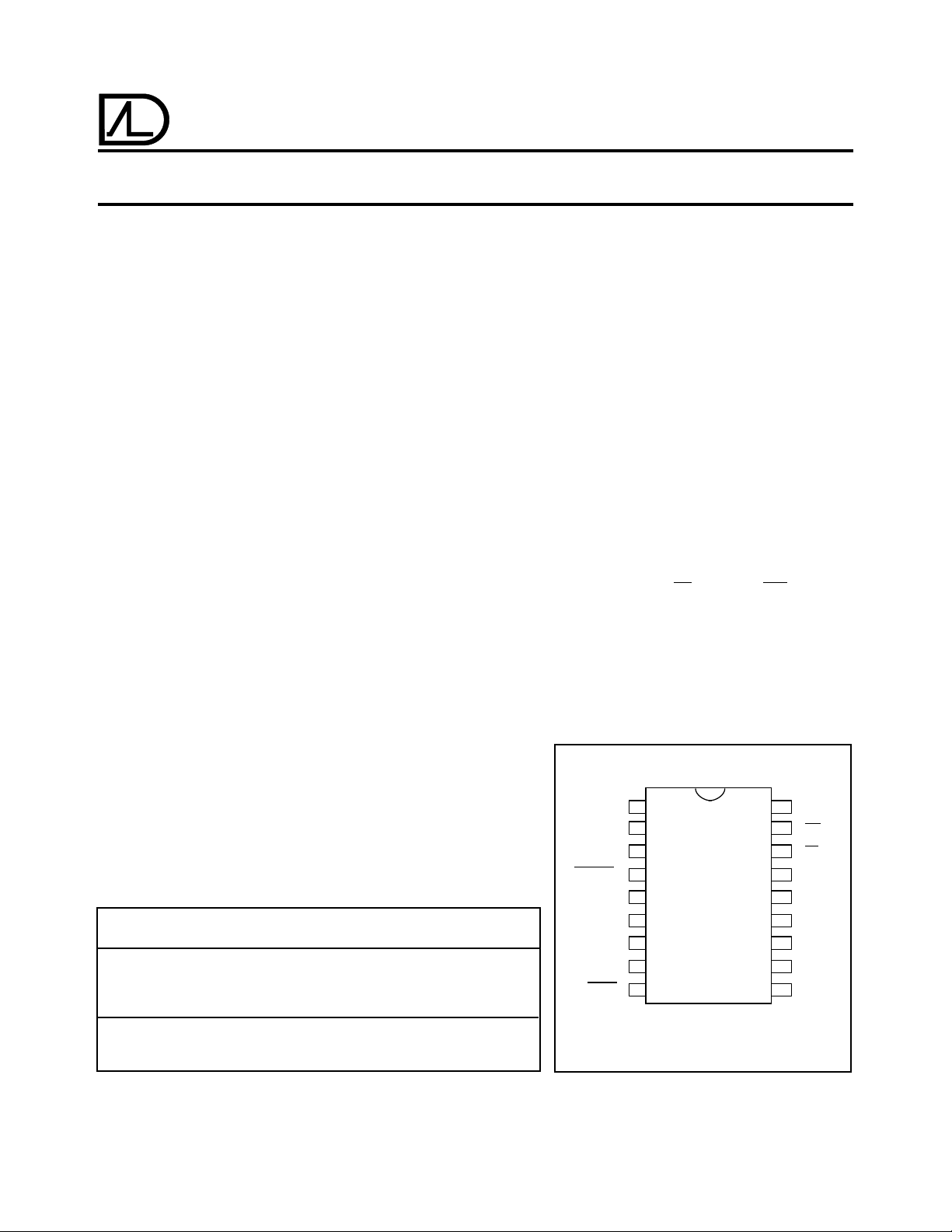
PIN CONFIGURATION
ALD521D
1
S
S
C
OUT
PWRUP
V
XTAL
OUT
XTAL
C
OUT
S
CLK
* Note: N/C - No Conncection
2
2
3
3
4
5
+
6
7
IN
8
9
PD, SD PACKAGE
18
17
16
15
14
13
12
11
10
S
1
DV
CS
D
OUT
DGND
C
S
B
A
N/C

GENERAL DESCRIPTION (cont'd)
The ALD521D implements all the four phases of the ALD500
or ALD500R, namely auto zero, integrate, deintegrate, and
integrator zero phases. It also provides direct logic interface
to CMOS logic families. The ALD521D operates from an
external clock or its internal oscillator circuit along with an
external crystal. The internal system clock of the ALD521D
runs at a divide by 4 rate of the crystal or external clock
frequency.
A Data Valid (DV) low output during the auto zero phase
indicates when a 24 bit data word is available for output while
during the other phases DV remains in logical 1 state.
The ALD521D has control input pins for power down
(PWRUP), Chip Select (CS) and Integration time selection
(S1, S2 and S3). These pins can all be interfaced directly to
any 5V CMOS logic or microcontroller. They can also be
connected to a PC parallel printer port directly. When not
used, or if no programming control is desired, these pins can
be wired directly to their respective desired logic state, either
V+ or DGND (Ground).
Upon power on, the ALD521D initiates a power-on initialization cycle and resets all internal counters and registers. Then
it check the status of the PWRUPpin. A logical 0 on PWRUP
power up the ALD521D and a logical 1 on PWRUP power
down the ALD521D. If the ALD521D detects a logical 1 state
on the PWRUP pin, it in turn powers down the ALD500R to
save power during non-active period. At the same time, the
crystal oscillator circuit of the ALD521D is also stopped to
conserve power consumption. In power down mode the
current consumption of the ALD521D and the ALD500R is
less than 28 µA. To start and power up the ALD521D again,
simply put a logical 0 on PWRUP. An external microcontroller
can therefore use this pin to control the ALD521D power-on
status. If power down feature is not used, then the PWRUP
pin must be grounded to leave the ALD521D in continuously
power-on mode.
Chip Select (CS) enable selection of the ALD521D controller
when this pin is at logical 0 (CS Input = GND). When not
selected, when the CS pin is at logical 1, the ALD521D places
the DV, D
OUT and SCLK pins in high impedance mode.
Multiple ALD521D devices can have these three pins wired
in parallel to a same external controller. When data is
required from a specific ALD521D, it is selected by having
its CS pin set at logical 0 state. The external controller can
send CS to only one ALD521D during each conversion cycle.
The CS must be valid for the duration of at least one complete
conversion cycle in order for the measurement data to be
valid. From an external controller, CS can be generated by
a latched output pin.
SELECTING INTEGRATION TIME
For maximum 50/60 cycle line power noise rejection, Integration time t
line power frequency. For example, t
msec, 33.333 msec, 66.667 msec, 100 msec, 200 msec and
INT must be picked as a multiple of the period of
INT
times of 16.667
300 msec maximize 60 Hz line power noise rejection; and 20
msec, 50 msec, 100 msec, 200 msec and 300 msec
maximize 50 Hz line power noise rejection. In general, the
longer the integration time , the better the noise rejection of
the line power noise, but it also takes longer to complete a
conversion cycle. A default recommended integration time of
100 msec offer the best tradeoff between noise performance, conversion time and 50/60 cycle line power noise
rejection. The 100 msec integration time also offers the
benefit of being universally optimal for both 50 cycle line
power noise rejection and 60 cycle line power noise
rejection.
ALD521D PIN CONFIGURATION FOR DIFFERENT INTEGRATION TIMES
SELECTIONS S1 S2 S3 INTEGRATION TIME APPROXIMATE NUMBER OF
PINS [18] [1] [2] CONVERSION/SECOND AC CYCLES
0 0 0 16.667ms 15 1
0 0 1 33.333ms 8 2
0 1 0 50.000ms 5 3
0 1 1 66.667ms 4 4
1 0 0 100.000 ms 3 6
1 0 1 166.667 ms 2 10
1 1 0 200.000 ms 1 12
1 1 1 300.000 ms 1 18
Note:"0" = GND; "1" = V
ALD512D Advanced Linear Devices 2
+
 Loading...