

Advanced Linear Devices Inc ALD500USWC, ALD500SWC, ALD500SC, ALD500PC, ALD500ASWC Datasheet
...
Operating Temperature Range *
0°C to +70°C0°C to +70°C0°C to +70°C
16-Pin 16-Pin 16-Pin Wide Body
Plastic Pin Small Outline Small Outline
Package Package (SOIC) Package (SOIC)
ALD500PC (16 bit) ALD500SC (16 bit) ALD500SWC (16 bit)
ALD500APC (17 bit) ALD500ASC (17 bit) ALD500ASWC (17 bit)
ALD500AUPC (18 bit) ALD500AUSC (18 bit) ALD500AUSWC (18 bit)
*
Contact factory for industrial temperature range
BENEFITS
• Wide dynamic signal range
• Very high noise immunity
• Low cost, simple functionality
• Automatic compensation and cancellation of
error sources
• Easy to use to acquire true 18 bit,17 bit, or
16 bit conversion and noise performance
• Inherently linear and stable with temperature
and component variations
FEATURES
• Resolution up to 18 bits plus sign bit
and over-range bit
• Accuracy independent of input source
impedances
• High input impedance of 10
12
Ω
• Inherently filters and integrates any
external noise spikes
• Differential analog input
• Wide bipolar analog input voltage
range ±3.5V
• Automatic zero offset compensation
• Low linearity error - as low as 0.002%
• Fast zero-crossing comparator - 1µs
• Low power dissipation - 6mW typical
• Automatic internal polarity detection
• Low input current - 2pA typical
• Microprocessor controlled conversion
• Optional digital control from a microcontroller, an ASIC, or a dedicated digital circuit
• Flexible conversion speed versus resolution
trade-off
ALD500AU/ALD500A/ALD500
ADVANCED
LINEAR
DEVICES, INC.
ORDERING INFORMATION
PRECISION INTEGRATING ANALOG PROCESSOR
APPLICATIONS
• 4 1/2 digits to 5 1/2 digits plus sign measurements
• Precision analog signal processor
• Precision sensor interface
• High accuracy DC measurement functions
• Portable battery operated instruments
• Computer peripheral
• PCMCIA
GENERAL DESCRIPTION
The ALD500AU/ALD500A/ALD500 are integrating dual slope analog
processors, designed to operate on ±5V power supplies for building
precision analog-to-digital converters. The ALD500AU/ALD500A/
ALD500 feature specifications suitable for 18 bit/17 bit/16 bit resolution
conversion, respectively. Together with three capacitors, one resistor,
a precision voltage reference, and a digital controller, a precision
Analog to Digital converter with auto zero can be implemented. The
digital controller can be implemented by an external microcontroller,
under either hardware (fixed logic) or software control. For ultra high
resolution applications, up to 23 bit conversion can be implemented with
an appropriate digital controller and software.
The ALD500 series of analog processors accept differential inputs and
the external digital controller first counts the number of pulses at a fixed
clock rate that a capacitor requires to integrate against an unknown
analog input voltage, then counts the number of pulses required to
deintegrate the capacitor against a known reference voltage. This
unknown analog voltage can then be converted by the microcontroller
to a digital word, which is translated into a high resolution number,
representing an accurate reading. This reading, when ratioed against
the reference voltage, yields an accurate, absolute voltage measurement
reading.
The ALD500 analog processors consist of on-chip digital control circuitry
to accept control inputs, integrating buffer amplifiers, analog switches,
and voltage comparators. It functions in four operating modes, or
phases, namely auto zero, integrate, deintegrate, and integrator zero
phases. At the end of a conversion, the comparator output goes from
high to low when the integrator crosses zero during deintegration.
ALD500 analog processors also provide direct logic interface to CMOS
logic families.
Rev. 1.02 © 1999 Advanced Linear Devices, Inc., 415 Tasman Drive, Sunnyvale, California 94089-1706, Tel: (408) 747-1155, Fax: (408) 747-1286
http://www.aldinc.com
PIN CONFIGURATION
V
+
1
2
3
14
15
16
4
13
B
5
12
A
V
+
REF
6
7
8
10
11
V
-
C
AZ
C
INT
B
UF
AGND
V
-
REF
C
+
REF
9
V
-
IN
V
+
IN
C
OUT
DGND
PC, SC, SWC PACKAGE
C
-
REF
ALD500
2 Advanced Linear Devices ALD500AU/ALD500A/ALD500
GENERAL THEORY OF OPERATION
Dual-Slope Conversion Principles of Operation
The basic principle of dual-slope integrating analog to digital
converter is simple and straightforward. A capacitor, C
INT
, is
charged with the integrator from a starting voltage, V
X
, for a
fixed period of time at a rate determined by the value of an
unknown input voltage, which is the subject of measurement.
Then the capacitor is discharged at a fixed rate, based on an
external reference voltage, back to V
X
where the discharge
time, or deintegration time, is measured precisely. Both the
integration time and deintegration time are measured by a
digital counter controlled by a crystal oscillator. It can be
demonstrated that the unknown input voltage is determined
by the ratio of the deintegration time and integration time, and
is directly proportional to the magnitude of the external reference
voltage.
The major advantages of a dual-slope converter are:
a. Accuracy is not dependent on absolute values of
integration time t
INT
and deintegration time t
DINT
, but is
dependent on their relative ratios. Long-term clock frequency
variations will not affect the accuracy. A standard crystal
controlled clock running digital counters is adequate to generate
very high accuracies.
b. Accuracy is not dependent on the absolute values of
R
INT and CINT
. as long as the component values do not vary
through a conversion cycle, which typically lasts less than 1
second.
c. Offset voltage values of the analog components, such
as V
X
, are cancelled out and do not affect accuracy.
d. Accuracy of the system depends mainly on the accuracy
and the stability of the voltage reference value.
e. Very high resolution, high accuracy measurements
can be achieved simply and at very low cost.
An inherent benefit of the dual slope converter system is noise
immunity. The input noise spikes are integrated (averaged to
near zero) during the integration periods. Integrating ADCs
are immune to the large conversion errors that plague
successive approximation converters and other high resolution
converters and perform very well in high-noise environments.
The slow conversion speed of the integrating converter provides
inherent noise rejection with at least a 20dB/decade attenuation
rate. Interference signals with frequencies at integral multiples
of the integration period are, theoretically, completely removed.
Integrating converters often establish the integration period to
reject 50/60Hz line frequency interference signals.
The relationship of the integrate and deintegrate (charge
and discharge) of the integrating capacitor values are
shown below:
V
INT
= VX - (V
IN
.
t
INT
/ R
INT
. C
INT
)
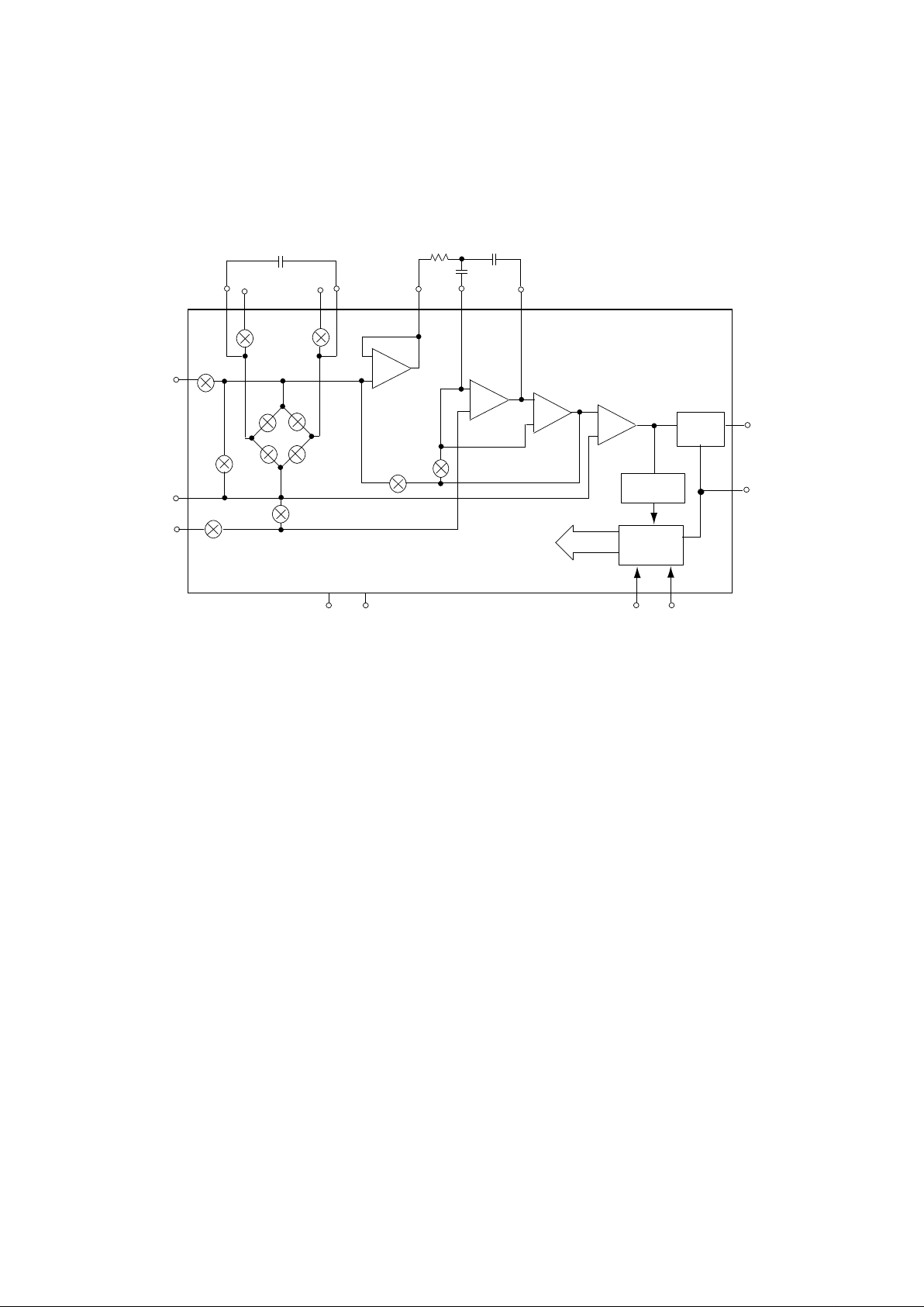
FIGURE 1. ALD 500 Functional Block Diagram
SW
-
R
-
+
-
+
+
-
+
-
(1)
(14)
(15)
C
OUT
DGND
Level
Shift
Polarity
Detection
Phase
Decoding
Logic
Comp2
Comp1
Integrator
Buffer
Analog
Switch
Control
Signals
Control Logic
A
B
AGND
(10)
(5)
(11)
(7)
(9) (8)
(6)
(4)
(2) (16)
(13)(12)
V
DD
V
SS
C
INT
C
INT
R
INT
C
AZ
C
AZ
C
-
REF
SW
AZ
SW
S
SWRSW
R
C
REF
SW
Az
SW
IN
SW
G
SW
IN
C
+
REF
V
+
REF
V
-
REF
SW
-
R
SW
+
R
SW
+
R
V
-
IN
V
+
IN
BUF
(3)
ALD500AU/ALD500A/ALD500 Advanced Linear Devices 3
(integrate cycle) (1)
V
X
= V
INT
- (V
REF
.
t
DINT
/ R
INT
.
C
INT
)
(deintegrate cycle) (2)
Combining equations 1 and 2 results in:
V
IN
/ V
REF
= -t
DINT
/ t
INT
(3)
where:
V
x
= An offset voltage used as starting voltage
V
INT
= Voltage change across C
INT
during t
INT
and
during t
DINT
(equal in magnitude)
V
IN
= Average, or an integrated, value of input voltage
to be measured during t
INT
(Constant VIN)
t
INT
= Fixed time period over which unknown voltage is
integrated
t
DINT
= Unknown time period over which a known
reference voltage is integrated
V
REF
= Reference Voltage
C
INT
= Integrating Capacitor value
R
INT
= Integrating Resistor value
Actual data conversion is accomplished in two phases: Input
Signal Integration Phase and Reference Voltage Deintegration
Phase.
The integrator output is initialized to 0V prior to the start of
Input Signal Integration Phase. During Input Signal Integration
Phase, internal analog switches connect V
IN
to the buffer
input where it is maintained for a fixed integration time period
(t
INT
). This fixed integration period is generally determined by
a digital counter controlled by a crystal oscillator. The
application of V
IN
causes the integrator output to depart 0V at
a rate determined by V
IN
and a direction determined by the
polarity of V
IN
.
The Reference Voltage Deintegration Phase is initiated
immediately after t
INT
, within 1 clock cycle. During Reference
Voltage Deintegration Phase, internal analog switches connect
a reference voltage having a polarity opposite that of V
IN
to
the integrator input. Simultaneously the same digital counter
controlled by the same crystal oscillator used above is used to
start counting clock pulses. The Reference Voltage
Deintegration Phase is maintained until the comparator output
inside the dual slope analog processor changes state, indicating
the integrator has returned to 0V. At that point the digital
counter is stopped. The Deintegration time period (t
DINT
), as
measured by the digital counter, is directly proportional to the
magnitude of the applied input voltage.
After the digital counter value has been read, the digital
counter, the integrator, and the auto zero capacitor are all
reset to zero through an Integrator Zero Phase and an Auto
Zero Phase so that the next conversion can begin again. In
practice, this process is usually automated so that analog-todigital conversion is continuously updated. The digital control
is handled by a microprocessor or a dedicated logic controller.
The output, in the form of a binary serial word, is read by a
microprocessor or a display adapter when desired.
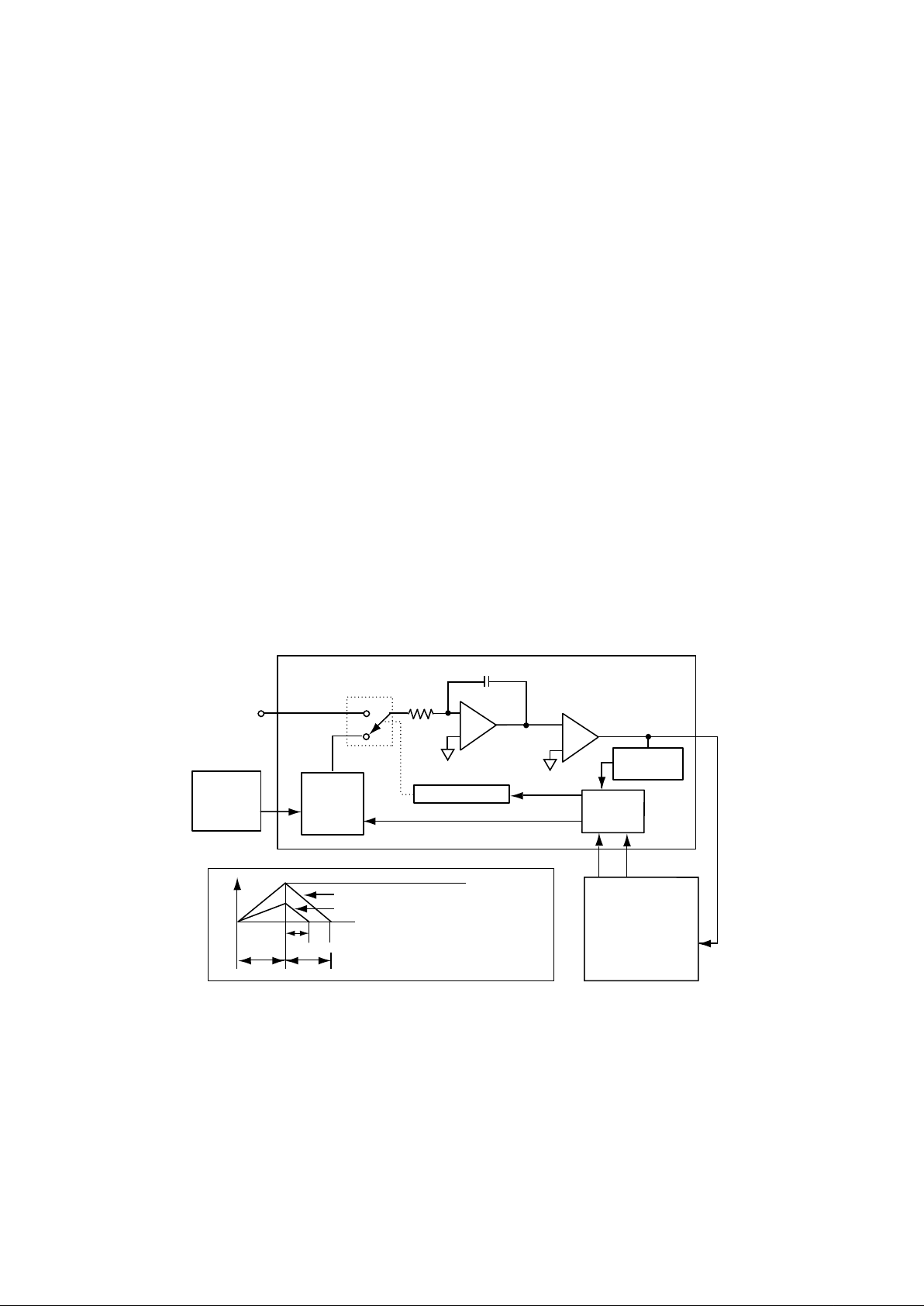
Figure 2. Basic Dual-Slope Converter
S1
C
INT
V
INT
R
INT
SWITCH DRIVER
CONTROL
LOGIC
POLARITY CONTROL
REF
SWITCHES
INTEGRATOR
COMPARATOR
PHASE
CONTROL
ANALOG
INPUT
(V
IN
)
OUTPUT
INTEGRATOR
V
IN ≈ VFULL SCALE
V
IN ≈ 1/2 VFULL SCALE
t
INT
t
DINT
V
INT
= 4.1V MAX
AB
Figure 2. Basic Dual-Slope Converter
+
+
-
VOLTAGE
REFERENCE
C
OUT
POLARITY
DETECTION
-
t
DINT
V
X ≈ 0
MICROCONTROLLER
(CONTROL LOGIC
+ COUNTER)

4 Advanced Linear Devices ALD500AU/ALD500A/ALD500
OPERATING ELECTRICAL CHARACTERISTICS
T
A
= 25°C V
+
= +5.0V V- = -5.0V (V
SUPPLY
= ±5.0 V) unless otherwise specified; CAZ = C
REF
= 0.47µf
500AU 500A 500
Parameter Symbol Min Typ Max Min Typ Max Min Typ Max Unit Test Conditions
Resolution 15 30 30 60 60 µV Note 1
Zero-Scale Z
SE
0.0025 0.003 0.005 %
Error 0.003 0.005 0.008 % 0°C to 70°C
End Point E
NL
0.005 0.005 0.010 0.005 0.015 % Notes 1, 2
Linearity 0.007 0.015 0.020 0°C to +70°C
Best Case N
L
0.0025 0.003 0.005 0.003 0.008 % Notes 1, 2
Straight Line
Linearity 0.004 0.008 0.015 0°C to +70°C
Zero-Scale TC
ZS
0.3 0.6 0.3 0.7 0.3 0.7 µV/°C0°C to +70°C
Temperature
Coefficient 0.15 0.3 0.15 0.35 0.15 0.35 ppm/°C Note 1
Full-Scale S
YE
0.005 0.008 0.01 %
Symmetry Error
(Rollover Error) 0.008 0.010 0.012 % 0°C to 70°C
Full-Scale TC
FS
1.3 1.3 1.3 ppm/°C0°C to +70°C
Temperature
Coefficient
Input I
IN
222pAV
IN
= 0V
Current
Common-Mode CMVR V-+1.5 V+-1.5 V-+1.5 V+-1.5 V-+1.5 V+-1.5 V
Voltage Range
Integrator V
INT
V-+0.9 V+-0.9 V-+0.9 V+-0.9 V-+0.9 V+-0.9 V
Output Swing
Analog Input V
IN
V-+1.5 V+-1.5 V-+1.5 V+-1.5 V-+1.5 V+-1.5 V AGND = 0V
Signal Range
Voltage V
REF
V-+1 V+-1 V-+1 V+-1 V-+1 V+-1 V
Reference
Range
ABSOLUTE MAXIMUM RATINGS
Supply voltage, V
+
13.2V
Differential input voltage range -0.3V to V
+
+0.3V
Power dissipation 600 mW
Operating temperature range PC, SC, SWC package 0°C to +70°C
Storage temperature range -65°C to +150°C
Lead temperature, 10 seconds +260°C
 Loading...