

Advanced Linear Devices Inc ALD4501SE, ALD4501PE, ALD4501DE Datasheet
ADVANCED
LINEAR
DEVICES, INC.
QUAD PRECISION HIGH SPEED MICROPOWER TIMER
ALD4501
GENERAL DESCRIPTION
The ALD4501 timer is a high performance QUAD monolithic timing circuit
built with advanced silicon gate CMOS technology. It offers the benefits of
high input impedance, thereby allowing smaller timing capacitors and
longer timing cycle; high speed with typical cycle time of 500ns; low power
dissipation for battery operated environment; and reduced supply current
spikes allowing smaller and lower cost decoupling capacitors. Each of the
four timers can be independently operated in either the monostable,
astable, or 50% duty cycle mode.
Each timer is capable of producing accurate time delays and oscillations in
both monostable and astable operation. It operates in the one-shot
(monostable) mode or 50% duty cycle free running oscillation mode with a
single resistor and one capacitor. The inputs and outputs are fully
compatible with CMOS, NMOS or TTL logic.
There are three matched internal resistors (approximately 200KΩ each)
that set the threshold and trigger levels at two-thirds and one-third respec-
+
tively of V
. These levels can be adjusted by using the control terminal.
When the trigger input is below the trigger level, the output is in the high
state and sourcing 2mA. When the threshold input is above the threshold
level at the same time the trigger input is above the trigger level, the internal
flip-flop is reset, the output goes to the low state and sinks up to 10mA. The
reset input overrides all other inputs and when it is active (reset voltage less
than 1V), the output is in the low state. All four timers share the same control
and reset pins so that timing functions are synchronized.
FEATURES
• High speed operation -- 2MHz typical oscillation at 5V
• Each discharge output sinking current: 40mA at 5V
• Guaranteed low operating supply voltage of 2 to 12V
• Each timer is functionally equivalent to NE555 with greatly expanded
high and low frequency ranges
• High speed, low power, monolithic CMOS technology
• Low supply current 150µA typical
• Extremely low trigger, threshold and reset currents -- 10pA typical
• Operates in both monostable and astable modes
• Fixed 50% duty cycle or adjustable duty cycle
• CMOS, NMOS and TTL compatible input/output
• Low supply current spikes
ORDERING INFORMATION
Operating Temperature Range *
-55°C to +125°C0°C to +70°C0°C to +70°C
20-Pin 20-Pin 20-Pin
CERDIP Small Outline Plastic Dip
Package Package (SOIC) Package
APPLICATIONS
.
• High speed one-shot (monostable)
pulse generation
• Precision timing
• Sequential timing
• Long delay timer
• Pulse width and pulse position
modulation
• Missing pulse detector
• Frequency divider
• Synchronized timer
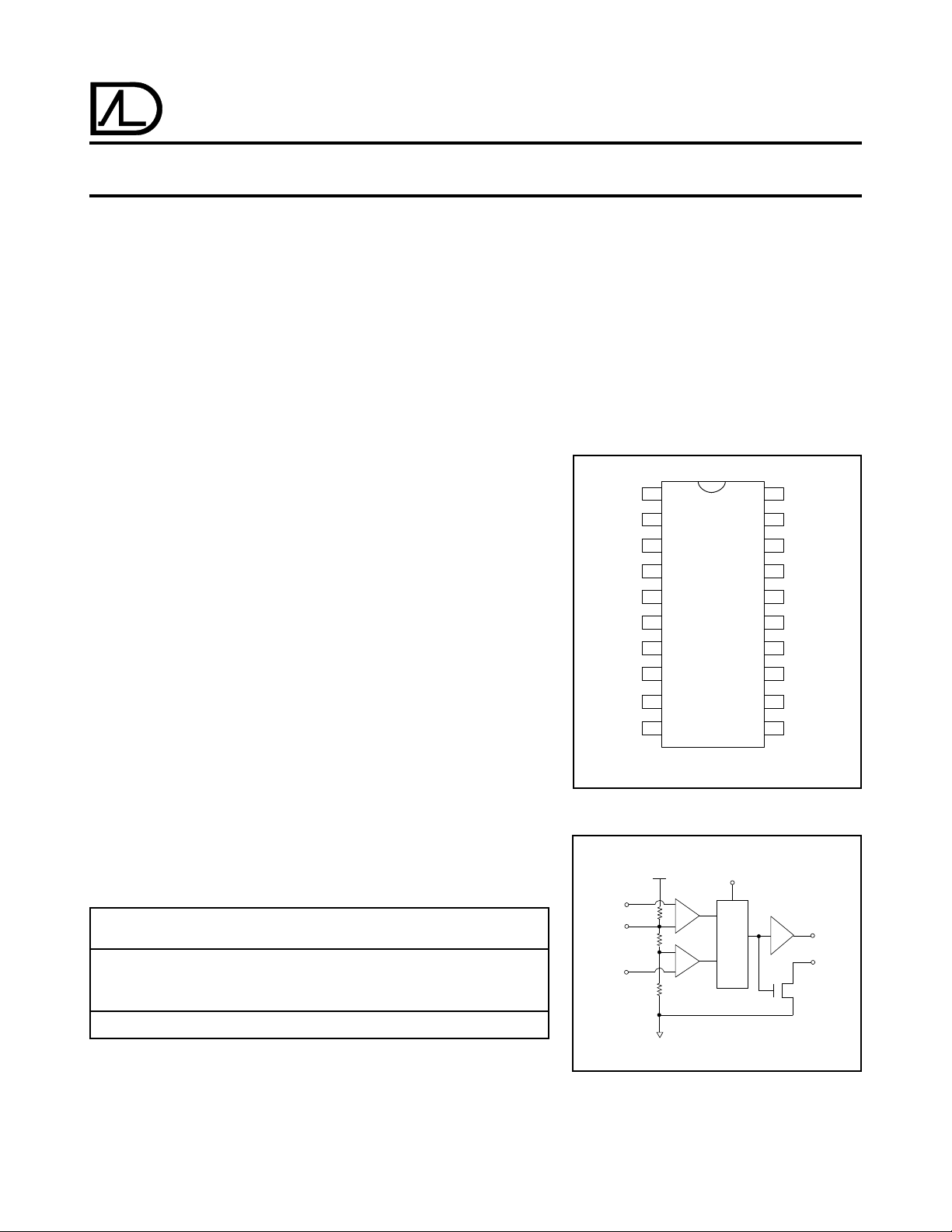
PIN CONFIGURATION
RST 1
DSC
1
TRIG
1
DSC
2
TRIG
2
DSC
3
TRIG
3
DSC
4
TRIG
4
-
V
2
3
4
5
6
7
8
9
10
DE, PE, SE PACKAGE
20
19
18
17
16
15
14
13
12
11
BLOCK DIAGRAM (EACH TIMER)
+
THRESHOLD
CONTROL
TRIGGER
V
R
R
R
RESET
R
S
+
V
OUT
THRES
OUT
THRES
OUT
THRES
OUT
THRES
CONT
OUTPUT
DISCHARGE
1
1
2
2
3
3
4
4
ALD4501 DE ALD4501 SE ALD4501 PE
* Contact factory for industrial temperature range
-
V
© 1998 Advanced Linear Devices, Inc. 415 T asman Drive, Sunnyvale, California 94089 -1706 Tel: (408) 747-1155 Fax: (408) 747-1286 http://www .aldinc.com

ABSOLUTE MAXIMUM RATINGS
Supply voltage, V
Input voltage range -0.3V to V+ +0.3V
Power dissipation 600 mW
Operating temperature range PE, SE package 0°C to + 70°C
Storage temperature range -65°C to +150°C
Lead temperature, 10 seconds +260°C
+
13.2V
DE package -55°C to +125°C
OPERATING ELECTRICAL CHARACTERISTICS
oC
= 25
T
A
Parameter Symbol Min Typ Max Unit Test Conditions
Supply Voltage V
Supply Current I
Timing error / Astable mode t
Initial Accuracy
Drift with Temperature
Drift with Supply Voltage
Threshold Voltage V
Trigger Voltage V
Trigger Current
Reset Voltage V
Reset Current
Threshold Current
Control Voltage Level V
Output Voltage Drop (Low) V
Output Voltage Drop (High) V
Rise Time of Output
Fall Time of Output
Discharge Transistor I
Leakage Current
+
V
= +5V unless otherwise specified
+
S
err
1
1
2
2
2
1
1
∆t/∆T 10.0 ppm/°CRA = 1KΩ
+
∆t/∆V
TH
TRIG
I
TRIG
RST
I
RST
I
TH
CONT
OL
OH
t
r
t
f
DL
3.233 3.333 3.433 V
1.567 1.667 1.767 V
0.4 0.7 1.0 V
3.233 3.333 3.433 V
212 V
150 270 µA Outputs Unloaded
1.0 2.6 % C = 0.1µF
0.1 %/V RB = 1KΩ
.01 0.4 nA
.01 0.4 nA
.01 0.4 nA
0.2 0.4 V I
4.2 4.6 V I
SINK
SOURCE
10 20 ns RL = 10MΩ
10 20 ns CL = 10pF
.01 nA
= 10mA
= -2mA
Discharge Voltage Drop V
DISC
0.5 1.0 V I
0.2 0.4 V I
Maximum Frequency R
Astable Mode f
Minimum Trigger Pulse Width
Notes:1 Sample tested parameters.
2
Consists of junction leakage currents with strong temperature dependence.
MAX
1
t
TRIG
2 MHz RB = 200Ω
50 100 ns
DISCHARGE
DISCHARGE
= 470Ω
A
=100pF
C
T
= 40mA
= 15mA
ALD4501 Advanced Linear Devices 9-2
 Loading...