

Page 1
ACR122L
-
USB
-
ACS
Design Specification
AACCRR11222222LL--DD11
Page 2

ACR122L
-
USB
-
ACS
Revision History
Version
V1.00 2010-6-24 Nathan.Li, Kit Au Initial Release
V1.01 2011-1-20 Kit Au
Date Prepared By Description
Page 3

ACR122L
-
USB
-
ACS
Table of Contents
Table of Contents ............................................................................................................... 3
1.0. Introduction............................................................................................................. 5
2.0. Feature..................................................................................................................... 5
3.0. Hardware Interfaces................................................................................................ 6
3.1.
USB Interface......................................................................................................................... 6
3.2.
LEDs ...................................................................................................................................... 6
3.3.
Buzzer .................................................................................................................................... 6
3.4.
SAM Interface ........................................................................................................................ 6
3.5.
LCD ........................................................................................................................................ 6
3.6.
PICC Interface (Contactless Smart Card).............................................................................. 6
4.0. Implementation ....................................................................................................... 7
4.1.
The ACR122L-USB is built based on the ST221 and PN5321 chips. ................................... 7
4.2.
Communication between the Host and the Contactless interface, SAM and Peripherals..... 8
5.0. Firmware Upgrade................................................................................................... 9
5.1.
With Press FW Key ................................................................................................................ 9
5.2.
Without Press FW Key ......................................................................................................... 11
6.0. PICC Interface Description................................................................................... 13
6.1.
6.2.
6.3.
ATR Generation ................................................................................................................... 13
Pseudo APDUs for Contactless Interface............................................................................ 15
6.2.1.
Direct Transmit via ScardTransmit............................................................................. 15
6.2.2.
Direct Transmit via ScardControl ............................................................................... 16
Pseudo APDU for Peripherals Control................................................................................. 16
6.3.1.
Pseudo APDU for LEDs and Buzzer Control ............................................................. 16
6.3.2.
Pseudo APDU for LEDs Control Enable .................................................................... 23
6.3.3.
Pseudo APDU for LEDs Control ................................................................................ 23
6.3.4.
Pseduo APDU for Buzzer Control .............................................................................. 24
6.3.5.
Pseudo APDU for Clear LCD ..................................................................................... 25
6.3.6.
Pseudo APDU for LCD Display (ASCII Mode) ........................................................... 26
6.3.7.
Pseudo APDU for LCD Display (GB Mode) ............................................................... 27
6.3.8.
Pseudo APDU for LCD Display (Graphic Mode)........................................................ 28
6.3.9.
Pseudo APDU for Scrolling LCD Current Display...................................................... 29
6.3.10.
6.3.11.
6.3.12.
Pseudo APDU for Pause LCD Scrolling..................................................................... 31
Pseudo APDU for Stop LCD Scrolling ....................................................................... 31
Pseudo APDU for LCD Contrast Control ................................................................... 31
6.4.
6.3.13.
6.4.1.
6.4.2.
Pseudo APDU for LCD Backlight Control .................................................................. 32
Escape APDU for Peripherals Control ................................................................................. 33
Escape APDU for LEDs and Buzzer Control ............................................................. 33
Escape APDU for LEDs Control Enable .................................................................... 38
Page 4

ACR122L
-
USB
-
ACS
6.4.3.
6.4.4.
6.4.5.
6.4.6.
6.4.7.
6.4.8.
6.4.9.
Escape APDU for LEDs Control................................................................................. 39
Escape APDU for Buzzer Control .............................................................................. 40
Escape APDU for Store Data one at Reader............................................................. 40
Escape APDU for Store Data two at Reader ............................................................. 41
Escape APDU for Read Data one from Reader......................................................... 41
Escape APDU for Read Data two from Reader ......................................................... 42
Escape APDU for Clear LCD ..................................................................................... 42
6.5.
6.6.
6.7.
6.4.10.
6.4.11.
6.4.12.
6.4.13.
6.4.14.
6.4.15.
6.4.16.
6.4.17.
6.6.1.
6.7.1.
6.7.2.
6.7.3.
6.7.4.
6.7.5.
Escape APDU for LCD Display (ASCII Mode) ........................................................... 43
Escape APDU for LCD Display (GB Mode) ............................................................... 45
Escape APDU for LCD Display (Graphic Mode)........................................................ 45
Escape APDU for Scrolling LCD Current Display ...................................................... 46
Escape APDU for Pause LCD Scrolling..................................................................... 48
Escape APDU for Stop LCD Scrolling........................................................................ 48
Escape APDU for LCD Contrast Control.................................................................... 48
Escape APDU for LCD Backlight Control................................................................... 49
Escape APDU for getting the Firmware Version.................................................................. 50
PICC Commands for General Purposes.............................................................................. 50
1. Get Data ................................................................................................................. 50
PICC Commands (T=CL Emulation) for MIFare 1K/4K MEMORY Cards ........................... 51
Load Authentication Keys .......................................................................................... 51
Authentication for MIFARE 1K/4K .............................................................................. 52
Read Binary Blocks .................................................................................................... 56
Update Binary Blocks ................................................................................................. 57
Value Block Related Commands ............................................................................... 58
7.0. Basic Program Flow for Contactless Applications ............................................. 62
7.1.
How to access PCSC Compliant Tags (ISO14443-4)? ....................................................... 63
7.2.
How to access DESFIRE Tags (ISO14443-4)? ................................................................... 66
7.3.
How to access FeliCa Tags (ISO18092)?............................................................................ 68
7.4.
How to access NFC Forum Type 1 Tags (ISO18092)? E.g. Jewel and Topaz Tags .......... 69
8.0. Basic Program Flow for SAM Applications ........................................................ 72
8.1.
How to access ACOS3 SAM Cards (ISO7816)? ................................................................. 73
9.0. Mechanical Design................................................................................................ 75
Page 5

1.0. Introduction
The ACR122L-USB is a module for accessing both contact and contactless cards with LCD Display. It
can support 3 SAMs access and ISO14443 Part1 - 4 Type A & B, MIFARE, FeliCa and NFC tags.
2.0. Feature
ISO 7816 Parts 1-4 Compliant for SAM Socket.
ISO 14443 Parts 1-4 Compliant for Contactless Smart Card Interface.
Support ISO14443 Part 4 Type A & B, MIFARE, FeliCa and NFC tags.
Built-in Antenna for contactless tags access.
3 X SAM Interface
4 LEDs.
Buzzer.
CCID Compliant for both SAM and PICC interface.
PCSC Compliant for Contact and Contactless Interfaces.
USB V2.0 Interface. (12M bps)
Device Firmware Upgradeable through the USB Interface.
Page 6

ACR122L
-
USB
-
ACS
3.0. Hardware Interfaces
3.1. USB Interface
The ACR122L-USB is connected to computer through USB as specified in the USB Specification 2.0.
ACR122L-USB is working in Full speed mode, i.e. 12 Mbps.
Pin Signal Function
1 V
2 D-
3 D+
4 GND
BUS
+5V power supply for the reader (~ 200mA)
Differential signal transmits data between ACR122L-USB and PC.
Differential signal transmits data between ACR122L-USB and PC.
Reference voltage level for power supply
3.2. LEDs
• 4 x User-controllable single color LEDs
• Can select control by firmware or by User
• From Left to right, the color of the LED is: Green, Blue, Yellow and Red
3.3. Buzzer
• User-controllable Mono-Tone buzzer.
• The default Buzzer State is OFF
3.4. SAM Interface
• 3 x SAMs socket is provided.
• Support ISO7816 Parts 1-3 T=0 ,T=1 cards
3.5. LCD
• User-controllable LCD
• User-controllable Yellow-Green Backlight
• 2 Line x 16 Character, 5 x 8 dot matrix, STN Yellow Green LCD Type
• 6 O’clock view angle
3.6. PICC Interface (Contactless Smart Card)
• 3 turns symmetric loop antenna. Center tapped.
• The estimated size = 46mm x 64mm.
• The loop inductance should be around ~ 1.6uH to 2.5uH
• Operating Distance for different Tags ~ up to 50mm (depend on the Tag)
• Only one Tag can be accessed at any one time.
Page 7
ACR122L
-
USB
-
ACS
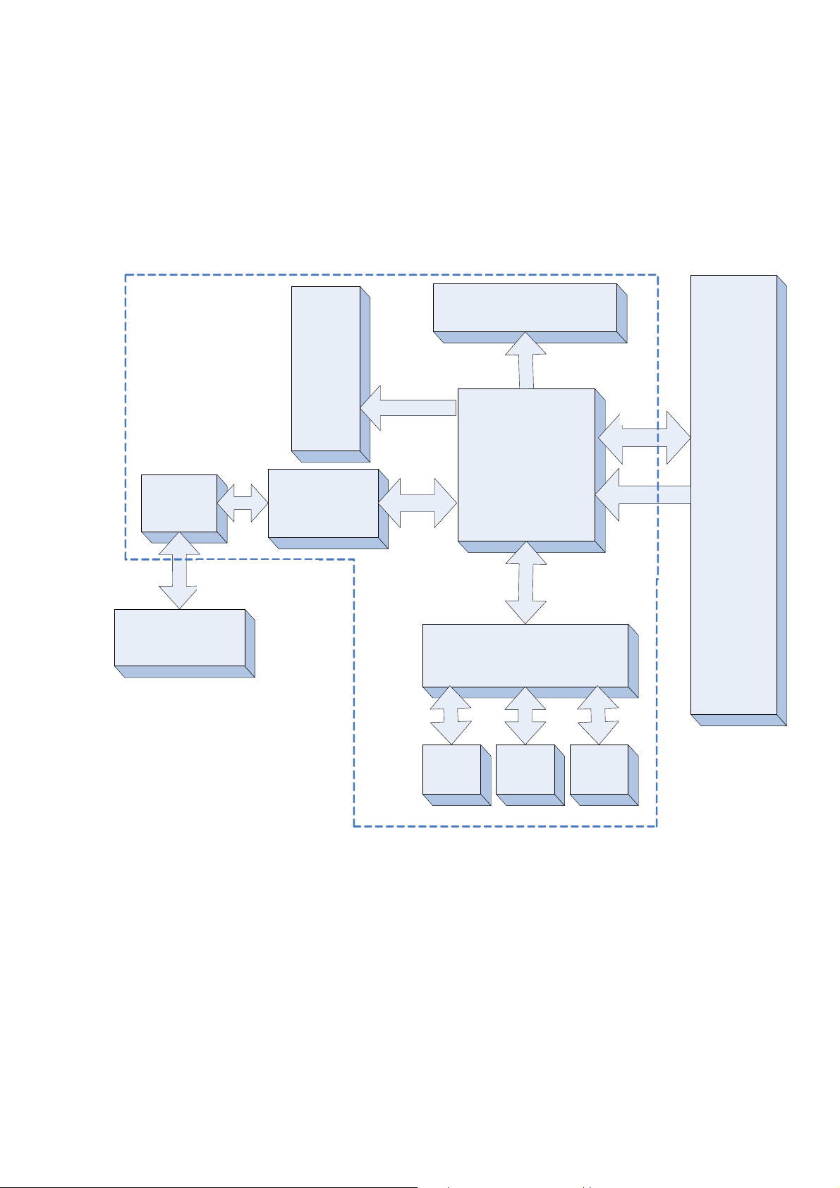
4.0. Implementation
4.1. The ACR122L-USB is built based on the ST221 and PN5321
chips.
LCD
Buzzer
&LED1
&LED2
&LED3
Built-In
Antenna
&LED4
PN532
NFC Interface
Chip
ST2211U
Host Controller
SPI
USB2.0
USB
USB
Firmware
Upgrade
PC
Windows
operating
system
PICC
Contactless Card
Contactless Interface
Carrier =13.56MHz
SAM1
ISO7816 Interface
Logic switch
SAM2 SAM3
Page 8
ACR122L
-
USB
-
ACS
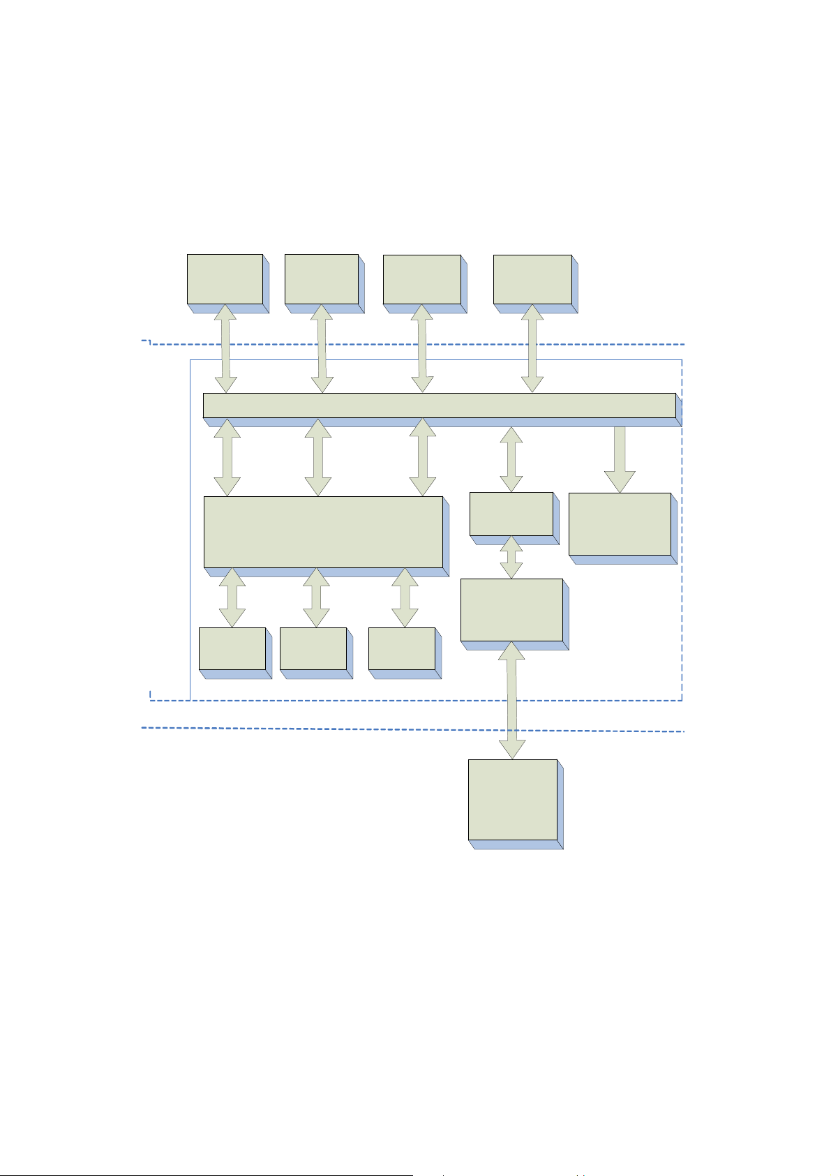
4.2. Communication between the Host and the Contactless
interface, SAM and Peripherals.
The Contactless interface & Peripherals are accessed through the use of Pseduo-APDUs.
The SAM interface are accessed through the use of standard APDUs.
PCSC
Driver
ACR122L-USB
PCSC SAM1
Interface
ACR122L-USB
PCSC SAM2
Interface
ACR122L-USB
PCSC SAM3
Interface
PCSC Layer
ACR122L-USB
PCSC PICC
Interface
USB
Interface
(CCID)
ACR122L-USB
SAM1
(Socket)
ISO 7816 Part1-4
+
T=0,T=1 SAM Interfaces
SAM2
(Socket)
SAM3
(Socket)
T=CL &T=1
Emulation
ISO 14443 Part1-4&
FeliCa
PICC Interface
PICC
(Built-In Antenna )
Peripherals
RF
Interface
Page 9
ACR122L
-
USB
-
ACS
5.0. Firmware Upgrade
5.1. With Press FW Key
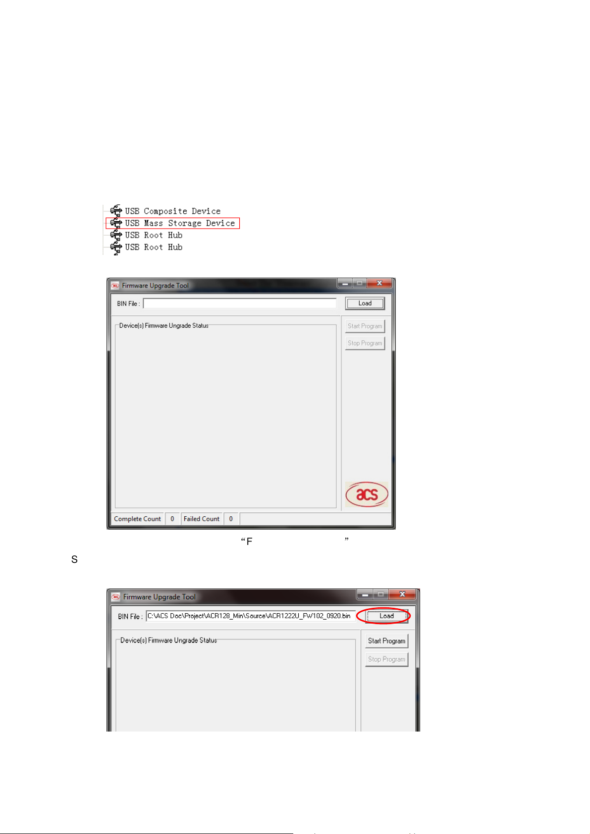
Step 1: Unplug the USB Cable from the PC.
Step 2: Press and Hold the FW Key
Step3: Plug the USB Cable to the PC.
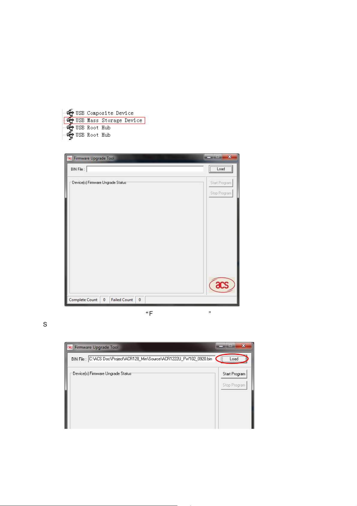
Step 4: The USB Mass Storage Device can be found in Device Manager, release the FW Key
Step 5: Execute the Firmware Upgrade Program:
“
Step 6: Pressing the “Load BIN” Button.
Select the “Firmware” file for Upload to the Reader
FW Upgrade Tool.exe”
Page 10
ACR122L
-
USB
-
ACS
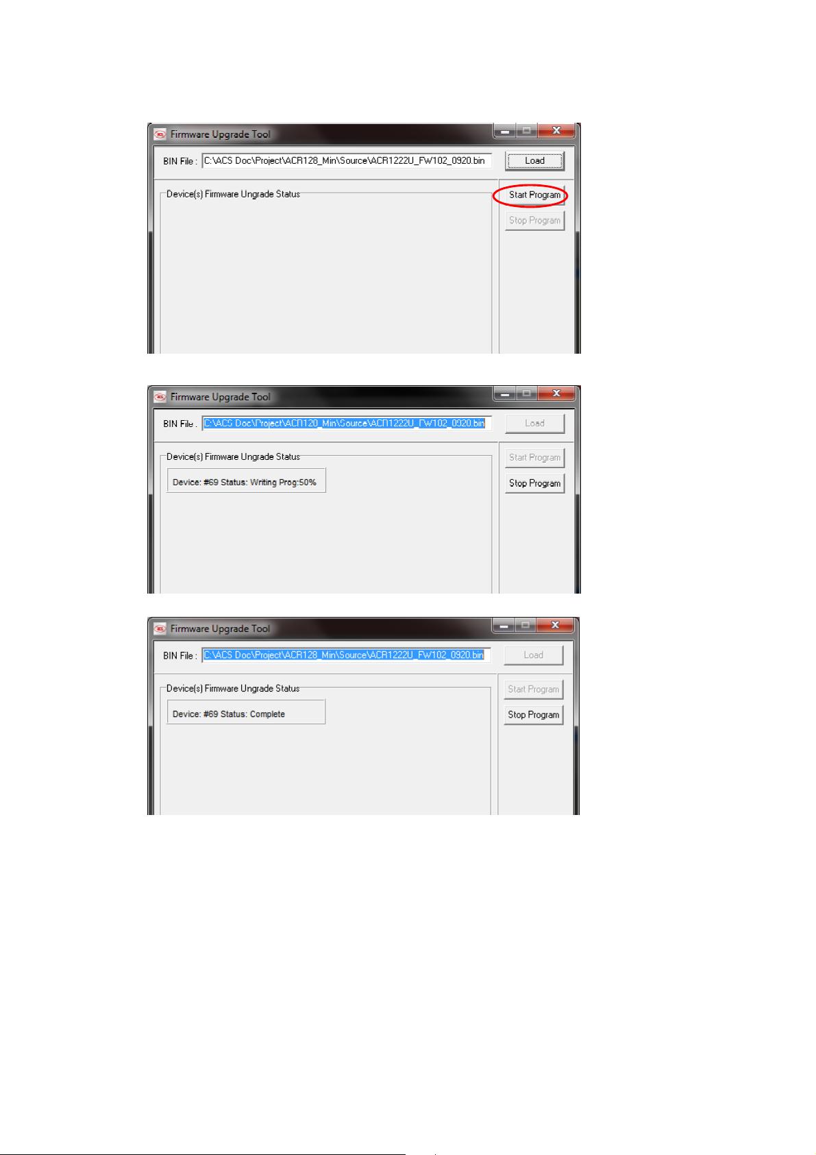
Step 7: Pressing the “Start Program” Button.
The firmware is being uploaded to the reader
The firmware upgrade is completed.
Step 8: Close the plastic covers. After that, reconnect the USB cord.
Noted:
If the upgrade firmware “fail”, please repeat do from steps 3 to 7.
Page 11
ACR122L
-
USB
-
ACS
5.2. Without Press FW Key
Step 1: Plug the USB Cable from the PC.
Step 2: Send EscapeCommand for Enter FW upgrade mode
Command = {E0 00 00 E0 00}.
Response = {E1 00 00 00 01 “Status”}
Step 3: The USB Mass Storage Device can be found in Device Manager, release the FW Key
Step 4: Execute the Firmware Upgrade Program:
“
Step 5: Pressing the “Load BIN” Button.
Select the “Firmware” file for Upload to the Reader
FW Upgrade Tool.exe”
Page 12

ACR122L
-
USB
-
ACS
Step 6: Pressing the “Start Program” Button.
The firmware is being uploaded to the reader
The firmware upgrade is completed.
Step 7: Close the plastic covers. After that, reconnect the USB cord.
Noted:
If the upgrade firmware “fails”, please using “5.1 With Press FW Key” Steps to do the upgrade
Page 13
ACR122L
-
USB
-
ACS
Pseudo APDUs for Contactless Interface and Peripherals Control
6.0. PICC Interface Description
6.1. ATR Generation
If the reader detects a PICC, an ATR will be sent to the PCSC driver for identifying the PICC.
1.1 ATR format for ISO 14443 Part 3 PICCs.
Byte
0 3B Initial Header
1 8N T0 Higher nibble 8 means: no TA1, TB1, TC1 only
2 80 TD1 Higher nibble 8 means: no TA2, TB2, TC2 only
3 01 TD2 Higher nibble 0 means no TA3, TB3, TC3, TD3
4
To
3+N
Value
(Hex)
80 T1 Category indicator byte, 80 means A status
4F Application identifier Presence Indicator
0C Length
RID Registered Application Provider Identifier (RID) #
Designation Description
TD1 is following.
Lower nibble N is the number of historical bytes
(HistByte 0 to HistByte N-1)
TD2 is following.
Lower nibble 0 means T = 0
following.
Lower nibble 1 means T = 1
indicator may be present in an optional
COMPACT-TLV data object
Tk
A0 00 00 03 06
SS Byte for standard
C0 .. C1
00 00 00 00 RFU RFU # 00 00 00 00
4+N UU TCK Exclusive-oring of all the bytes T0 to Tk
e.g. ATR for MIFare 1K = {3B 8F 80 01 80 4F 0C A0 00 00 03 06 03 00 01 00 00 00 00 6A}
Length (YY) = 0x0C
RID = {A0 00 00 03 06} (PC/SC Workgroup)
Standard (SS) = 03 (ISO14443A, Part 3)
Card Name (C0 .. C1) = {00 01} (MIFare 1K)
Bytes for card name
Page 14

ACR122L
-
USB
-
ACS
Card Name (C0 .. C1)
00 01: Mifare 1K
00 02: Mifare 4K
00 03: Mifare Ultralight
00 26: Mifare Mini
F0 04: Topaz and Jewel
F0 11: FeliCa 212K
F0 12: FeliCa 424K
FF [SAK]: undefined tags
1.2 ATR format for ISO 14443 Part 4 PICCs.
Byte
0 3B Initial Header
1 8N T0 Higher nibble 8 means: no TA1, TB1, TC1 only
2 80 TD1 Higher nibble 8 means: no TA2, TB2, TC2 only
3 01 TD2 Higher nibble 0 means no TA3, TB3, TC3, TD3
to
3 + N
Value
(Hex)
XX T1 4
XX
XX
XX
Designation Description
TD1 is following.
Lower nibble N is the number of historical bytes
(HistByte 0 to HistByte N-1)
TD2 is following.
Lower nibble 0 means T = 0
following.
Lower nibble 1 means T = 1
Historical Bytes:
Tk
ISO14443A:
The historical bytes from ATS response. Refer to
the ISO14443-4 specification.
ISO14443B:
The higher layer response from the ATTRIB
response (ATQB). Refer to the ISO14443-3
specification.
4+N UU TCK Exclusive-oring of all the bytes T0 to Tk
E.g 1. ATR for DESFire = { 3B 81 80 01 80 80 } // 6 bytes of ATR
Page 15

ACR122L
-
USB
-
ACS
Hint: Use the APDU “FF CA 01 00 00” to distinguish the ISO14443A-4 and ISO14443B-4 PICCs, and
retrieve the full ATS if available. ISO14443A-3 or ISO14443B-3/4 PICCs do have ATS returned.
APDU Command = FF CA 01 00 00
APDU Response = 06 75 77 81 02 80 90 00
ATS = {06 75 77 81 02 80}
E.g 2. ATR for ST19XRC8E = { 3B 8C 80 01 50 12 23 45 56 12 53 54 4E 33 81 C3 55}
// 12 bytes of ATQB, No CRC-B
ATQB = {50 12 23 45 56 12 53 54 4E 33 81 C3}
6.2. Pseudo APDUs for Contactless Interface
ACR128MiniU comes with two primitive commands for this purpose. <Class 0xFF>
6.2.1. Direct Transmit via ScardTransmit
To send a Pseudo APDU (PN532 and TAG Commands), and the Response Data will be returned.
Table 1.0A: Direct Transmit Command Format (Length of the PN532_TAG Command + 5 Bytes)
Command
Direct
Transmit
Lc: Number of Bytes to Send (1 Byte)
Maximum 255 bytes.
Data In: PN532_TAG Command
The data to be sent to the PN532 and Tag.
Table 1.0B: Direct Transmit Response Format (Response Length + 2 Bytes)
Response
Result
Class INS P1 P2 Lc Data In
0xFF 0x00 0x00 0x00 Number
of Bytes
to send
Data Out
PN532_TAG
Response
SW1 SW2
PN532_TAG
Command
Data Out: PN532_TAG Response
PN532_TAG Response returned by the reader.
Data Out: SW1 SW2
Page 16

ACR122L
-
USB
-
ACS
Status Code returned by the reader.
Table 1.0C: Status Code
Results
Success 90 00 The operation is completed successfully.
Error
Checksum Error
SW1 SW2 Meaning
63 00 The operation is failed.
63 27 The checksum of the Response is
wrong.
6.2.2. Direct Transmit via ScardControl
Command = {E0 00 00 24 XX “PN532_TAG Command”}
Response = {E1 00 00 00 YY “PN532_TAG Response”}
XX = Length of the “PN532_TAG Command”
YY= Length of the “PN532_TAG Response”
6.3. Pseudo APDU for Peripherals Control
6.3.1. Pseudo APDU for LEDs and Buzzer Control
This APDU is used to control the states of the LED_0, LED_1 and Buzzer.
Table 2.0A: LED_0, LED_1 and Buzzer Control Command Format (9 Bytes)
Command
LEDs and
Buzzer
LED Control
P2: LED State Control
Table 2.0B: LED_0, LED_1 and Buzzer Control Format (1 Byte)
CMD Item Description
Bit 0 Final LED_1 State 1 = On; 0 = Off
Bit 1 Final LED_0 State 1 = On; 0 = Off
Bit 2 LED_1 State Mask 1 = Update the State
Class INS P1 P2 Lc Data In
0xFF 0x00 0x40 LED
State
Control
0x04 Blinking Duration Control
0 = No change
(4 Bytes)
Bit 3 LED_0 State Mask 1 = Update the State
Page 17
ACR122L
-
USB
-
ACS
0 = No change
Bit 4 Initial LED_1 Blinking State 1 = On; 0 = Off
Bit 5 Initial LED_0 Blinking State 1 = On; 0 = Off
Bit 6 LED_1 Blinking Mask 1 = Blink
0 = Not Blink
Bit 7 LED_0 Blinking Mask 1 = Blink
0 = Not Blink
Data In: Blinking Duration Control
Table 2.0C: LED_0, LED_1 Blinking Duration Control Format (4 Bytes)
Byte 0 Byte 1 Byte 2 Byte 3
T1 Duration
Initial Blinking State
(Unit = 100ms)
Byte 3: Link to Buzzer. Control the buzzer state during the LED Blinking.
0x00: The buzzer will not turn on
0x01: The buzzer will turn on during the T1 Duration
0x02: The buzzer will turn on during the T2 Duration
0x03: The buzzer will turn on during the T1 and T2 Duration.
Data Out: SW1 SW2. Status Code returned by the reader.
Table 2.0D: Status Code
Results
Success 90 Current LED State The operation is completed successfully.
Error
SW1 SW2 Meaning
63 00 The operation is failed.
T2 Duration
Toggle Blinking State
(Unit = 100ms)
Number of
repetition
Link to Buzzer
Table 3.0E: Current LED State (1 Byte)
Status Item Description
Bit 0 Current LED_1 LED 1 = On; 0 = Off
Bit 1 Current LED_0 LED 1 = On; 0 = Off
Bits 2 – 7 Reserved
Page 18

ACR122L
-
USB
-
ACS
Remark:
1. The LED State operation will be performed after the LED Blinking operation is completed.
2. The LED will not be changed if the corresponding LED Mask is not enabled.
3. The LED will not be blinking if the corresponding LED Blinking Mask is not enabled. Also, the
number of repetition must be greater than zero.
4. T1 and T2 duration parameters are used for controlling the duty cycle of LED blinking and Buzzer
Turn-On duration.
For example, if T1=1 and T2=1, the duty cycle = 50%. #Duty Cycle = T1 / (T1 + T2).
5. To control the buzzer only, just set the P2 “LED State Control” to zero.
6. The make the buzzer operating, the “number of repetition” must greater than zero.
7. To control the LED only, just set the parameter “Link to Buzzer” to zero.
Page 19

ACR122L
-
USB
-
ACS
Example 1: To read the existing LED State.
// Assume both LED_0 and LED_1 are OFF initially //
// Not link to the buzzer //
APDU = “FF 00 40 00 04 00 00 00 00”
Response = “90 00”. LED_0 and LED_1 LEDs are OFF.
Example 2: To turn on LED_0 and LED_1
// Assume both LED_0 and LED_1 are OFF initially //
// Not link to the buzzer //
APDU = “FF 00 40 0F 04 00 00 00 00”
Response = “90 03”. LED_0 and LED_1 are ON,
#To turn off both LED_0 and LED_1, APDU = “FF 00 40 0C 04 00 00 00 00”
Example 3: To turn off the LED_1 only, and left the LED_0 unchanged.
// Assume both LED_0 and LED_1 are ON initially //
// Not link to the buzzer //
APDU = “FF 00 40 04 04 00 00 00 00”
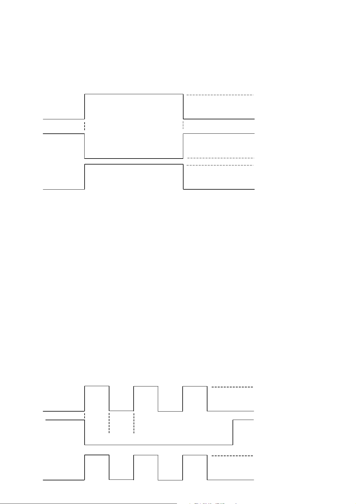
Response = “90 02”. LED_0 is not changed (ON); LED_1 is OFF,
LED_1 On
LED_1 Off
LED_0 On
LED_0 Off
Page 20
ACR122L
-
USB
-
ACS
Example 4: To turn on the LED_1 for 2 sec. After that, resume to the initial state
// Assume the LED_1 is initially OFF, while the LED_0 is initially ON. //
// The LED_1 and buzzer will turn on during the T1 duration, while the LED_0 will turn off during the
T1 duration. //
LED_1 On
T1 = 2000ms
T2 = 0ms
LED_1 Off
LED_0 On
LED_0 Off
Buzzer On
Buzzer Off
1Hz = 1000ms Time Interval = 500ms ON + 500 ms OFF
T1 Duration = 2000ms = 0x14
T2 Duration = 0ms = 0x00
Number of repetition = 0x01
Link to Buzzer = 0x01
APDU = “FF 00 40 50 04 14 00 01 01”
Response = “90 02”
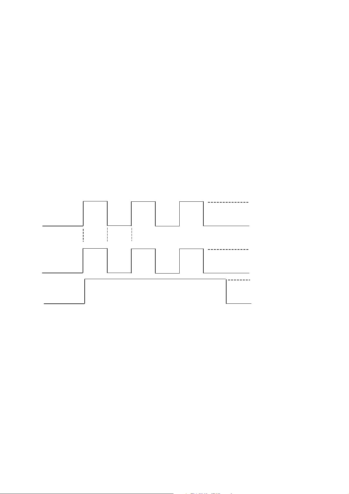
Example 5: To blink the LED_1 of 1Hz for 3 times. After that, resume to initial state
// Assume the LED_1 is initially OFF, while the LED_0 is initially ON. //
// The Initial LED_1 Blinking State is ON. Only the LED_1 will be blinking.
// The buzzer will turn on during the T1 duration, while the LED_0 will turn off during both the T1 and
T2 duration.
// After the blinking, the LED_0 will turn ON. The LED_1 will resume to the initial state after the
blinking //
LED_1 On
LED_1 Off
LED_0 On
T1 = 500ms
T2 = 500ms
LED_0 Off
Buzzer On
Buzzer Off
Page 21
ACR122L
-
USB
-
ACS
T1 =
T2 =
1Hz = 1000ms Time Interval = 500ms ON + 500 ms OFF
T1 Duration = 500ms = 0x05
T2 Duration = 500ms = 0x05
Number of repetition = 0x03
Link to Buzzer = 0x01
APDU = “FF 00 40 50 04 05 05 03 01”
Response = “90 02”
Example 6: To blink the LED_1 and LED_0 of 1Hz for 3 times
// Assume both the LED_0 and LED_1 are initially OFF. //
// Both Initial LED_0 and LED_1 Blinking States are ON //
// The buzzer will turn on during both the T1 and T2 duration//
LED_1 On
500ms
1Hz = 1000ms Time Interval = 500ms ON + 500 ms OFF
T1 Duration = 500ms = 0x05
T2 Duration = 500ms = 0x05
Number of repetition = 0x03
Link to Buzzer = 0x03
APDU = “FF 00 40 F0 04 05 05 03 03”
Response = “90 00”
500ms
LED_1 Off
LED_0 On
LED_0 Off
Buzzer On
Buzzer Off
Example 7: To blink the LED_1 and LED_0 in turn of 1Hz for 3 times
// Assume both LED_0 and LED_1 LEDs are initially OFF. //
// The Initial LED_1 Blinking State is ON; The Initial LED_0 Blinking States is OFF //
Page 22

ACR122L
-
USB
-
ACS
T1 =
T2 =
// The buzzer will turn on during the T1 duration//
LED_1 On
LED_1 Off
500ms
1Hz = 1000ms Time Interval = 500ms ON + 500 ms OFF
T1 Duration = 500ms = 0x05
T2 Duration = 500ms = 0x05
Number of repetition = 0x03
Link to Buzzer = 0x01
APDU = “FF 00 40 D0 04 05 05 03 01”
Response = “90 00”
500ms
LED_0 On
LED_0 Off
Buzzer On
Buzzer Off
Page 23
ACR122L
-
USB
-
ACS
6.3.2. Pseudo APDU for LEDs Control Enable
This APDU is used to set the LEDs Control Enable/ Disable by user.
Default “Disable”, the LED perform by the firmware
Table 3.0A: Clear LCD Command Format (5 Bytes)
Command
LED Control 0xFF 0x00 0x43 bLEDCtrl 0x00
P2: bLEDCtrl (1 Byte)
CMD Description
0x00 Disable LEDs Control by user
0xFF Enable LEDs Control by user
Data Out: SW1 SW2.
Table 3.0B: Status Code
Results
Success 90 00 The operation is completed successfully.
Error
Class INS P1 P2 Lc
SW1 SW2 Meaning
63 00 The operation is failed.
6.3.3. Pseudo APDU for LEDs Control
This APDU is used to control 4 LEDs
Table 4.0A: Clear LCD Command Format (5 Bytes)
Command
LED Control 0xFF 0x00 0x41 bLEDsState 0x00
P2: bLEDsState
LED_0, LED_1, LED_2 and LED_3 Control Format (1 Byte)
CMD Item Description
Bit 0 LED_0 State 1 = On; 0 = Off
Bit 1 LED_1 State 1 = On; 0 = Off
Bit 2 LED_2 State 1 = On; 0 = Off
Bit 3 LED_3 State 1 = On; 0 = Off
Bits 4 – 7 Reserved
Class INS P1 P2 Lc
Page 24
ACR122L
-
USB
-
ACS
Data Out: SW1 SW2.
Table 4.0B: Status Code
Results
Success 90 00 The operation is completed successfully.
Error
SW1 SW2 Meaning
63 00 The operation is failed.
6.3.4. Pseduo APDU for Buzzer Control
This APDU is used to control Buzzer
Table 5.0A: Buzzer Control Command Format (5 Bytes)
Command
Buzzzer Control 0xFF 0x00 0x42 0x00 0x03 Buzzer Control
Data In: Buzzer Control
Table 5.0B: Buzzer On/Off Duration Control Format (4 Bytes)
Class INS P1 P2 Lc Data In
(3 Bytes)
Byte 0 Byte 1 Byte 2
T1 Duration
On State
(Unit = 100ms)
Data Out: SW1 SW2.
Table 5.0C: Status Code
Results
Success 90 00 The operation is completed successfully.
Error
SW1 SW2 Meaning
63 00 The operation is failed.
T2 Duration
Off State
(Unit = 100ms)
Number of
repetition
Page 25

ACR122L
-
USB
-
ACS
6.3.5. Pseudo APDU for Clear LCD
This APDU is used to clear all content show on the LCD
Table 6.0A: Clear LCD Command Format (5 Bytes)
Command
Clear LCD 0xFF 0x00 0x60 0x00 0x00
Data Out: SW1 SW2.
Table 6.0B: Status Code
Results
Success 90 00 The operation is completed successfully.
Error
Class INS P1 P2 Lc
SW1 SW2 Meaning
63 00 The operation is failed.
Page 26

ACR122L
-
USB
-
ACS
6.3.6. Pseudo APDU for LCD Display (ASCII Mode)
This APDU is used to Display LCD Message in ASCII Mode
Table 7.0A: LCD Display Command Format (5 Bytes + LCD Message Length)
Command Class INS P1 P2 Lc Data In
(Max. 16Bytes)
LCD Display 0xFF Option
Byte
0x68 LCD XY Position
LCD
Message
LCD Message
Length
INS: Option Byte (1 Byte)
CMD Item Description
Bit 0 Character Bold Font 1 = Bold; 0 = Normal
Bit 1 - 3 Reserved
Bit 4 - 5 Table Index
00 = Fonts Set A
01 = Fonts Set B
10 = Fonts Set C
Bits 6 – 7 Reserved
P2: LCD XY Position
The Character to be displayed on the LCD position specified by DDRAM Address
Please follow the DDRAM table below for the LCD character position’s representation
For Fonts Set 1 and 2,
1 2 3 4 5 6 7 8 9 10 11 12 13 14 15 16 DISPLAY
1st LINE 00 01 02 03 04 05 06 07 08 09 0A 0B 0C 0D 0E 0F
2nd LINE 40 41 42 43 44 45 46 47 48 49 4A 4B 4C 4D 4E 4F
POSITION
LCD XY
POSITION
For Fonts Set 3,
1 2 3 4 5 6 7 8 9 10 11 12 13 14 15 16 DISPLAY
1st LINE 00 01 02 03 04 05 06 07 08 09 0A 0B 0C 0D 0E 0F
2nd LINE 20 21 22 23 24 25 26 27 28 29 2A 2B 2C 2D 2E 2F
3rd LINE 40 41 42 43 44 45 46 47 48 49 4A 4B 4C 4D 4E 4F
4th LINE 60 61 62 63 64 65 66 67 68 69 6A 6B 6C 6D 6E 6F
POSITION
LCD XY
POSITION
Lc: LCD Message Length
The length of the LCD message (max. 0x10); If the message length is longer than the number of
character that the LCD screen’s can be shown, then the redundant character will not be shown on the
LCD
Page 27

ACR122L
-
USB
-
ACS
Data In:
The data to be sent to LCD, maximum 16 Character for each line
Please follow the Fonts tables (selected by INS Bit 4 - 5) below for the LCD Character Index
Remarks: Size of the Characters in Fonts Set A and Fonts Set B is 8x16, but size of the Characters in
Fonts Set C is 8x8
LCD Message
Character Set A Character Set B Character Set C
Data Out: SW1 SW2.
Table 7.0B: Status Code
Results
Success 90 00 The operation is completed successfully.
Error 63 00 The operation is failed.
SW1 SW2 Meaning
6.3.7. Pseudo APDU for LCD Display (GB Mode)
This APDU is used to Display LCD Message in GB Mode
Table 8.0A: LCD Display Command Format (5 Bytes + LCD Message Length)
Command
LCD Display 0xFF Option
INS: Option Byte (1 Byte)
CMD Item Description
Class INS P1 P2 Lc Data In
(Max. 16 Bytes)
LCD Message
Byte
0x69 LCD XY Position
LCD
Message
Length
Bit 0 Character Bold Font 1 = Bold; 0 = Normal
Bit 1 - 7 Reserved
P2: LCD XY Position
The Character to be displayed on the LCD position specified by DDRAM Address
Page 28

ACR122L
-
USB
-
ACS
Please follow the DDRAM table below for the LCD character position’s representation
1 2 3 4 5 6 7 8 9 10 11 12 13 14 15 16 DISPLAY
FIRST LINE 00 01 02 03 04 05 06 07
SECOND LINE 40 41 42 43 44 45 46 47
POSITION
LCD XY
POSITION
Lc: LCD Message Length
The length of the LCD message (max. 0x10); If the message length is longer than the number of
character that the LCD screen’s can be shown, then the redundant character will not be shown on the
LCD
The length of the LCD message should multiple of 2 because each Chinese Character (GB code)
should be contain two bytes
Data In:
LCD Message
The data to be sent to LCD, maximum 8(2 x 8bit each character) Character for each line
Please follow the Fonts table of GB Coding
Data Out: SW1 SW2.
Table 8.0B: Status Code
Results
SW1 SW2 Meaning
Success 90 00 The operation is completed successfully.
Error 63 00 The operation is failed.
6.3.8. Pseudo APDU for LCD Display (Graphic Mode)
This APDU is used to Display LCD Message in Graphic Mode
Table 9.0A: LCD Display Command Format (5 Bytes + LCD Message Length)
Command
LCD Display 0xFF 0x00 0x6A Line Index
Class INS P1 P2 Lc Data In
(max. 128 Bytes)
Pixel Data
Pixel Data
Length
P2: Line Index
To set which line to start to update the LCD Display
Refer to Below LCD Display Position
Lc:
Pixel Data
Length
The length of the pixel data (max. 0x80)
Data In:
Pixel Data
The pixel data to be sent to LCD for display
LCD Display Position (Total LCD Size: 128x32):
Byte 0x00 (X = 0x00) Byte 0x01 (X = 0x01) … Byte 0x0F (X = 0x0F)
0x00
7 6 5 4 3 2 1 0 7 6 5 4 3 2 1 0 … 7 6 5 4 3 2 1 0
Page 29

ACR122L
-
USB
-
ACS
X
-axis
Line Index
0x01
0x02
0x03
0x04
0x05
0x06
0x07
0x08
0x09
… …
0x1F
Data Out: SW1 SW2.
Table 9.0B: Status Code
Results
SW1 SW2 Meaning
Success 90 00 The operation is completed successfully.
Error 63 00 The operation is failed.
6.3.9. Pseudo APDU for Scrolling LCD Current Display
This APDU is used to set scrolling feature of the Current LCD Display
Table 10.0A: Scrolling LCD Command Format (5 Bytes + LCD Message Length)
Command
LCD Display 0xFF 0x00 0x6D 0x00
Data In: Scroll Ctrl
Table 10.0B: Scrolling Control Format (6 Bytes)
Byte 0 Byte 1 Byte 2 Byte 3 Byte 4 Byte 5
X Position Y Position Scrolling Range
Class INS P1 P2 Lc Data In
(6 Bytes)
0x06
(Horizontal)
Scrolling Range
(Vertical)
Scroll Ctrl
Refresh Speed
Ctrl
Scrolling
Direction
X Position: Horizontal Start Up Position, Ref to LCD Display Position Below
Y Position: Vertical Start Up Position, Ref to LCD Display Position Below
LCD Display Position (Total LCD Size: 128x32):
Byte 0x00 (X = 0x00) Byte 0x01 (X = 0x01) … Byte 0x0F (X = 0x0F)
0x00
0x01
0x02
0x03
0x04
7 6 5 4 3 2 1 0 7 6 5 4 3 2 1 0 … 7 6 5 4 3 2 1 0
Page 30

ACR122L
-
USB
-
ACS
0x05
0x06
0x07
0x08
0x09
… …
0x1F
Scrolling Range (Horizontal): How many 8 pixels in Horizontal after X position will be scrolled
Scrolling Range (vertical): How many pixels in Vertical after Y position will be scrolled
Refresh Speed Ctrl:
Bit0~Bit3 – how many pixel move pre scrolling
Bit4~Bit7 – Scrolling period
Bit7 Bit6 Bit5 Bit4 Scrolling period
0 0 0 0 1 Unit
0 0 0 1 3 Units
0 0 1 0 5 Units
0 0 1 1 7 Units
0 1 0 0 17 Units
0 1 0 1 19 Units
0 1 1 0 21 Units
0 1 1 1 23 Units
1 0 0 0 129 Units
1 0 0 1 131 Units
1 0 1 0 133 Units
1 0 1 1 135 Units
1 1 0 0 145 Units
1 1 0 1 147 Units
1 1 1 0 149 Units
1 1 1 1 151 Units
Scrolling Direction: the Scrolling Direction
Bit1 Bit0 Scrolling Direction
0 0 From Left to Right
0 1 From Right to Left
1 0 From Top to Bottom
1 1 From Bottom to Top
Data Out: SW1 SW2.
Table 10.0C: Status Code
Results
Success 90 00 The operation is completed successfully.
SW1 SW2 Meaning
Page 31

ACR122L
-
USB
-
ACS
Error 63 00 The operation is failed.
6.3.10. Pseudo APDU for Pause LCD Scrolling
This APDU is used to Pause the LCD Scrolling set before
To resume the scrolling, send again the scrolling LCD command (5.10) to perform
Table 11.0A: Pause Scrolling Command Format (5 Bytes)
Command
Clear LCD 0xFF 0x00 0x6E 0x00 0x00
Data Out: SW1 SW2.
Table 11.0B: Status Code
Results
Success 90 00 The operation is completed successfully.
Error
Class INS P1 P2 Lc
SW1 SW2 Meaning
63 00 The operation is failed.
6.3.11. Pseudo APDU for Stop LCD Scrolling
This APDU is used to stop the LCD Scrolling set before, the LCD display will back to normal display
position
Table 12.0A: Stop Scrolling LCD Command Format (5 Bytes)
Command
Class INS P1 P2 Lc
Clear LCD 0xFF 0x00 0x6F 0x00 0x00
Data Out: SW1 SW2.
Table 12.0B: Status Code
Results
Success 90 00 The operation is completed successfully.
Error
SW1 SW2 Meaning
63 00 The operation is failed.
6.3.12. Pseudo APDU for LCD Contrast Control
This APDU is used to Control the LCD Contrast
Table 13.0A: LCD Contrast Control Command Format (5 Bytes)
Page 32

ACR122L
-
USB
-
ACS
Command
LCD Contrast
Control
P2: Contrast Control
The value range is between 0x00 to 0x0F. It is as large as brighten on contrast. Otherwise the
contrast will been darken.
Data Out: SW1 SW2.
Table 13.0B: Status Code
Results
Success 90 00 The operation is completed successfully.
Error 63 00 The operation is failed.
Class INS P1 P2 Lc
0xFF 0x00 0x6C Contrast Control 0x00
SW1 SW2 Meaning
6.3.13. Pseudo APDU for LCD Backlight Control
This APDU is used to Control the LCD Backlight
Table 14.0A: LCD Backlight Control Command Format (5 Bytes)
Command
LCD Backlight
Control
P2: Backlight Control
Table 14.0B: Backlight Control Format (1 Byte)
CMD Description
0x00 LCD Backlight Off
0xFF LCD Backlight On
Data Out: SW1 SW2.
Table 14.0C: Status Code
Class INS P1 P2 Lc
0xFF 0x00 0x64 Backlight
Control
0x00
Results
Success 90 00 The operation is completed successfully.
Error
SW1 SW2 Meaning
63 00 The operation is failed.
Page 33

ACR122L
-
USB
-
ACS
6.4. Escape APDU for Peripherals Control
All the command is the same as Part 5.3 for Terminal Application Layer, but the command is
sent by Escape APDU.
6.4.1. Escape APDU for LEDs and Buzzer Control
This APDU is used to control the states of the LED_0, LED_1 and Buzzer.
Table 2.0A: LED_0, LED_1 and Buzzer Control Command Format (9 Bytes)
Command
LEDs and
Buzzer
LED Control
P2: LED State Control
Table 2.0B: LED_0, LED_1 and Buzzer Control Format (1 Byte)
CMD Item Description
Bit 0 Final LED_1 State 1 = On; 0 = Off
Bit 1 Final LED_0 State 1 = On; 0 = Off
Bit 2 LED_1 State Mask 1 = Update the State
Bit 3 LED_0 State Mask 1 = Update the State
Bit 4 Initial LED_1 Blinking State 1 = On; 0 = Off
Class INS P1 P2 Lc Data In
0xFF 0x00 0x40 LED
State
Control
0x04 Blinking Duration Control
0 = No change
0 = No change
(4 Bytes)
Bit 5 Initial LED_0 Blinking State 1 = On; 0 = Off
Bit 6 LED_1 Blinking Mask 1 = Blink
0 = Not Blink
Bit 7 LED_0 Blinking Mask 1 = Blink
0 = Not Blink
Data In: Blinking Duration Control
Table 2.0C: LED_0, LED_1 Blinking Duration Control Format (4 Bytes)
Byte 0 Byte 1 Byte 2 Byte 3
T1 Duration
Initial Blinking State
(Unit = 100ms)
Byte 3: Link to Buzzer. Control the buzzer state during the LED Blinking.
0x00: The buzzer will not turn on
T2 Duration
Toggle Blinking State
(Unit = 100ms)
Number of
repetition
Link to Buzzer
Page 34

ACR122L
-
USB
-
ACS
0x01: The buzzer will turn on during the T1 Duration
0x02: The buzzer will turn on during the T2 Duration
0x03: The buzzer will turn on during the T1 and T2 Duration.
Data Out: SW1 SW2. Status Code returned by the reader.
Table 2.0D: Status Code
Results
Success 90 Current LED State The operation is completed successfully.
Error
Table 3.0E: Current LED State (1 Byte)
Status Item Description
Bit 0 Current LED_1 LED 1 = On; 0 = Off
Bit 1 Current LED_0 LED 1 = On; 0 = Off
Bits 2 – 7 Reserved
Remark:
8. The LED State operation will be performed after the LED Blinking operation is completed.
9. The LED will not be changed if the corresponding LED Mask is not enabled.
10. The LED will not be blinking if the corresponding LED Blinking Mask is not enabled. Also, the
number of repetition must be greater than zero.
11. T1 and T2 duration parameters are used for controlling the duty cycle of LED blinking and Buzzer
Turn-On duration.
SW1 SW2 Meaning
63 00 The operation is failed.
For example, if T1=1 and T2=1, the duty cycle = 50%. #Duty Cycle = T1 / (T1 + T2).
12. To control the buzzer only, just set the P2 “LED State Control” to zero.
13. The make the buzzer operating, the “number of repetition” must greater than zero.
14. To control the LED only, just set the parameter “Link to Buzzer” to zero.
Page 35

ACR122L
-
USB
-
ACS
Example 1: To read the existing LED State.
// Assume both LED_0 and LED_1 are OFF initially //
// Not link to the buzzer //
APDU = “FF 00 40 00 04 00 00 00 00”
Response = “90 00”. LED_0 and LED_1 LEDs are OFF.
Example 2: To turn on LED_0 and LED_1
// Assume both LED_0 and LED_1 are OFF initially //
// Not link to the buzzer //
APDU = “FF 00 40 0F 04 00 00 00 00”
Response = “90 03”. LED_0 and LED_1 are ON,
#To turn off both LED_0 and LED_1, APDU = “FF 00 40 0C 04 00 00 00 00”
Example 3: To turn off the LED_1 only, and left the LED_0 unchanged.
// Assume both LED_0 and LED_1 are ON initially //
// Not link to the buzzer //
APDU = “FF 00 40 04 04 00 00 00 00”
Response = “90 02”. LED_0 is not changed (ON); LED_1 is OFF,
LED_1 On
LED_1 Off
LED_0 On
LED_0 Off
Page 36

ACR122L
-
USB
-
ACS
Example 4: To turn on the LED_1 for 2 sec. After that, resume to the initial state
// Assume the LED_1 is initially OFF, while the LED_0 is initially ON. //
// The LED_1 and buzzer will turn on during the T1 duration, while the LED_0 will turn off during the
T1 duration. //
LED_1 On
T1 = 2000ms
T2 = 0ms
LED_1 Off
LED_0 On
LED_0 Off
Buzzer On
Buzzer Off
1Hz = 1000ms Time Interval = 500ms ON + 500 ms OFF
T1 Duration = 2000ms = 0x14
T2 Duration = 0ms = 0x00
Number of repetition = 0x01
Link to Buzzer = 0x01
APDU = “FF 00 40 50 04 14 00 01 01”
Response = “90 02”
Example 5: To blink the LED_1 of 1Hz for 3 times. After that, resume to initial state
// Assume the LED_1 is initially OFF, while the LED_0 is initially ON. //
// The Initial LED_1 Blinking State is ON. Only the LED_1 will be blinking.
// The buzzer will turn on during the T1 duration, while the LED_0 will turn off during both the T1 and
T2 duration.
// After the blinking, the LED_0 will turn ON. The LED_1 will resume to the initial state after the
blinking //
LED_1 On
LED_1 Off
LED_0 On
T1 = 500ms
T2 = 500ms
LED_0 Off
Buzzer On
Buzzer Off
Page 37

ACR122L
-
USB
-
ACS
T1 =
T2 =
1Hz = 1000ms Time Interval = 500ms ON + 500 ms OFF
T1 Duration = 500ms = 0x05
T2 Duration = 500ms = 0x05
Number of repetition = 0x03
Link to Buzzer = 0x01
APDU = “FF 00 40 50 04 05 05 03 01”
Response = “90 02”
Example 6: To blink the LED_1 and LED_0 of 1Hz for 3 times
// Assume both the LED_0 and LED_1 are initially OFF. //
// Both Initial LED_0 and LED_1 Blinking States are ON //
// The buzzer will turn on during both the T1 and T2 duration//
LED_1 On
500ms
1Hz = 1000ms Time Interval = 500ms ON + 500 ms OFF
T1 Duration = 500ms = 0x05
T2 Duration = 500ms = 0x05
Number of repetition = 0x03
Link to Buzzer = 0x03
APDU = “FF 00 40 F0 04 05 05 03 03”
Response = “90 00”
500ms
LED_1 Off
LED_0 On
LED_0 Off
Buzzer On
Buzzer Off
Example 7: To blink the LED_1 and LED_0 in turn of 1Hz for 3 times
// Assume both LED_0 and LED_1 LEDs are initially OFF. //
// The Initial LED_1 Blinking State is ON; The Initial LED_0 Blinking States is OFF //
Page 38

ACR122L
-
USB
-
ACS
T1 =
T2 =
// The buzzer will turn on during the T1 duration//
LED_1 On
LED_1 Off
500ms
1Hz = 1000ms Time Interval = 500ms ON + 500 ms OFF
T1 Duration = 500ms = 0x05
T2 Duration = 500ms = 0x05
Number of repetition = 0x03
Link to Buzzer = 0x01
APDU = “FF 00 40 D0 04 05 05 03 01”
Response = “90 00”
500ms
6.4.2. Escape APDU for LEDs Control Enable
LED_0 On
LED_0 Off
Buzzer On
Buzzer Off
This APDU is used to set the LEDs Control Enable/ Disable by user.
Default “Disable”, the LED perform by the firmware
Table 3.0A: Clear LCD Command Format (5 Bytes)
Command
LED Control 0xFF 0x00 0x43 bLEDCtrl 0x00
P2: bLEDCtrl (1 Byte)
CMD Description
0x00 Disable LEDs Control by user
0xFF Enable LEDs Control by user
Data Out: SW1 SW2.
Table 3.0B: Status Code
Results
Class INS P1 P2 Lc
SW1 SW2 Meaning
Page 39

ACR122L
-
USB
-
ACS
Success 90 00 The operation is completed successfully.
Error
63 00 The operation is failed.
6.4.3. Escape APDU for LEDs Control
This APDU is used to control 4 LEDs
Table 4.0A: Clear LCD Command Format (5 Bytes)
Command
LED Control 0xFF 0x00 0x41 bLEDsState 0x00
P2: bLEDsState
LED_0, LED_1, LED_2 and LED_3 Control Format (1 Byte)
CMD Item Description
Bit 0 LED_0 State 1 = On; 0 = Off
Bit 1 LED_1 State 1 = On; 0 = Off
Class INS P1 P2 Lc
Bit 2 LED_2 State 1 = On; 0 = Off
Bit 3 LED_3 State 1 = On; 0 = Off
Bits 4 – 7 Reserved
Data Out: SW1 SW2.
Table 4.0B: Status Code
Results
Success 90 00 The operation is completed successfully.
Error
SW1 SW2 Meaning
63 00 The operation is failed.
Page 40

ACR122L
-
USB
-
ACS
6.4.4. Escape APDU for Buzzer Control
This APDU is used to control Buzzer
Table 5.0A: Buzzer Control Command Format (5 Bytes)
Command
Buzzzer Control 0xFF 0x00 0x42 0x00 0x03 Buzzer Control
Data In: Buzzer Control
Table 5.0B: Buzzer On/Off Duration Control Format (4 Bytes)
Byte 0 Byte 1 Byte 2
T1 Duration
On State
(Unit = 100ms)
Data Out: SW1 SW2.
Table 5.0C: Status Code
Results
Success 90 00 The operation is completed successfully.
Error
Class INS P1 P2 Lc Data In
(3 Bytes)
T2 Duration
Off State
(Unit = 100ms)
SW1 SW2 Meaning
63 00 The operation is failed.
Number of
repetition
6.4.5. Escape APDU for Store Data one at Reader
This APDU is used to store a data up to 256 byte to the reader.
Table 5.0A: Store Data One Command Format (5 Bytes)
Command
Buzzzer Control 0xFF 0x00 0x4a 0x00 0x00
Data LenH : The high byte of the data length
Data LenL : The low byte of the data length
Data Out: SW1 SW2.
Table 5.0C: Status Code
Results
Success 90 00 The operation is completed successfully.
Error
Class INS P1 P2 Lc Data
LenH
SW1 SW2 Meaning
63 00 The operation is failed.
Data
LenL
data
Data
Page 41

ACR122L
-
USB
-
ACS
6.4.6. Escape APDU for Store Data two at Reader
This APDU is used to store a data up to 256 byte to the reader.
Table 5.0A: Store Data One Command Format (5 Bytes)
Command
Buzzzer Control 0xFF 0x00 0x4b 0x00 0x00
Data LenH : The high byte of the data length
Data LenL : The low byte of the data length
Data Out: SW1 SW2.
Table 5.0C: Status Code
Results
Success 90 00 The operation is completed successfully.
Error
Class INS P1 P2 Lc Data
LenH
SW1 SW2 Meaning
63 00 The operation is failed.
Data
LenL
data
Data
6.4.7. Escape APDU for Read Data one from Reader
This APDU is used to store a data up to 256 byte to the reader.
Table 5.0A: Store Data One Command Format (5 Bytes)
Command
Buzzzer Control 0xFF 0x00 0x4c 0x00 0x00
Data LenH : The high byte of the data length
Data LenL : The low byte of the data length
Data Out: SW1 SW2.
Table 5.0C: Status Code
Results
data the data return for the reader
Class INS P1 P2 Lc Data
LenH
data
Data
LenL
data
Data
Page 42

ACR122L
-
USB
-
ACS
6.4.8. Escape APDU for Read Data two from Reader
This APDU is used to store a data up to 256 byte to the reader.
Table 5.0A: Store Data two Command Format (5 Bytes)
Command
Buzzzer Control 0xFF 0x00 0x4d 0x00 0x00
Data LenH : The high byte of the data length
Data LenL : The low byte of the data length
Data Out:
Results
data the data return for the reader
Class INS P1 P2 Lc Data
LenH
data
6.4.9. Escape APDU for Clear LCD
This APDU is used to clear all content show on the LCD
Table 6.0A: Clear LCD Command Format (5 Bytes)
Data
LenL
data
Data
Command
Clear LCD 0xFF 0x00 0x60 0x00 0x00
Data Out: SW1 SW2.
Table 6.0B: Status Code
Results
Success 90 00 The operation is completed successfully.
Error
Class INS P1 P2 Lc
SW1 SW2 Meaning
63 00 The operation is failed.
Page 43

ACR122L
-
USB
-
ACS
6.4.10. Escape APDU for LCD Display (ASCII Mode)
This APDU is used to Display LCD Message in ASCII Mode
Table 7.0A: LCD Display Command Format (5 Bytes + LCD Message Length)
Command Class INS P1 P2 Lc Data In
(Max. 16Bytes)
LCD Display 0xFF Option
Byte
0x68 LCD XY Position
LCD
Message
LCD Message
Length
INS: Option Byte (1 Byte)
CMD Item Description
Bit 0 Character Bold Font 1 = Bold; 0 = Normal
Bit 1 - 3 Reserved
Bit 4 - 5 Table Index
00 = Fonts Set A
01 = Fonts Set B
10 = Fonts Set C
Bits 6 – 7 Reserved
P2: LCD XY Position
The Character to be displayed on the LCD position specified by DDRAM Address
Please follow the DDRAM table below for the LCD character position’s representation
For Fonts Set 1 and 2,
1 2 3 4 5 6 7 8 9 10 11 12 13 14 15 16 DISPLAY
1st LINE 00 01 02 03 04 05 06 07 08 09 0A 0B 0C 0D 0E 0F
2nd LINE 40 41 42 43 44 45 46 47 48 49 4A 4B 4C 4D 4E 4F
POSITION
LCD XY
POSITION
For Fonts Set 3,
1 2 3 4 5 6 7 8 9 10 11 12 13 14 15 16 DISPLAY
1st LINE 00 01 02 03 04 05 06 07 08 09 0A 0B 0C 0D 0E 0F
2nd LINE 20 21 22 23 24 25 26 27 28 29 2A 2B 2C 2D 2E 2F
3rd LINE 40 41 42 43 44 45 46 47 48 49 4A 4B 4C 4D 4E 4F
4th LINE 60 61 62 63 64 65 66 67 68 69 6A 6B 6C 6D 6E 6F
POSITION
LCD XY
POSITION
Lc: LCD Message Length
The length of the LCD message (max. 0x10); If the message length is longer than the number of
character that the LCD screen’s can be shown, then the redundant character will not be shown on the
LCD
Data In:
LCD Message
The data to be sent to LCD, maximum 16 Character for each line
Page 44

ACR122L
-
USB
-
ACS
Please follow the Fonts tables (selected by INS Bit 4 - 5) below for the LCD Character Index
Remarks: Size of the Characters in Fonts Set A and Fonts Set B is 8x16, but size of the Characters in
Fonts Set C is 8x8
Character Set A Character Set B Character Set C
Data Out: SW1 SW2.
Table 7.0B: Status Code
Results
Success 90 00 The operation is completed successfully.
Error 63 00 The operation is failed.
SW1 SW2 Meaning
Page 45

6.4.11. Escape APDU for LCD Display (GB Mode)
This APDU is used to Display LCD Message in GB Mode
Table 8.0A: LCD Display Command Format (5 Bytes + LCD Message Length)
Command
LCD Display 0xFF Option
Class INS P1 P2 Lc Data In
(Max. 16 Bytes)
LCD Message
Byte
0x69 LCD XY Position
LCD
Message
Length
INS: Option Byte (1 Byte)
CMD Item Description
Bit 0 Character Bold Font 1 = Bold; 0 = Normal
Bit 1 - 7 Reserved
P2: LCD XY Position
The Character to be displayed on the LCD position specified by DDRAM Address
Please follow the DDRAM table below for the LCD character position’s representation
1 2 3 4 5 6 7 8 9 10 11 12 13 14 15 16 DISPLAY
FIRST LINE 00 01 02 03 04 05 06 07
SECOND LINE 40 41 42 43 44 45 46 47
POSITION
LCD XY
POSITION
Lc: LCD Message Length
The length of the LCD message (max. 0x10); If the message length is longer than the number of character
that the LCD screen’s can be shown, then the redundant character will not be shown on the LCD
The length of the LCD message should multiple of 2 because each Chinese Character (GB code) should be
contain two bytes
Data In:
LCD Message
The data to be sent to LCD, maximum 8(2 x 8bit each character) Character for each line
Please follow the Fonts table of GB Coding
Data Out: SW1 SW2.
Table 8.0B: Status Code
Results
SW1 SW2 Meaning
Success 90 00 The operation is completed successfully.
Error 63 00 The operation is failed.
6.4.12. Escape APDU for LCD Display (Graphic Mode)
This APDU is used to Display LCD Message in Graphic Mode
Table 9.0A: LCD Display Command Format (5 Bytes + LCD Message Length)
Command
Class INS P1 P2 Lc Data In
LCD Display 0xFF 0x00 0x6A Line Index
Pixel Data
(max. 128 Bytes)
Pixel Data
Length
Page 46

ACR122L
-
USB
-
ACS
X
P2: Line Index
To set which line to start to update the LCD Display
Refer to Below LCD Display Position
Lc:
Pixel Data
Length
The length of the pixel data (max. 0x80)
Data In:
Pixel Data
The pixel data to be sent to LCD for display
LCD Display Position (Total LCD Size: 128x32):
-axis
Line Index
0x00
0x01
0x02
0x03
0x04
0x05
0x06
0x07
0x08
0x09
… …
0x1F
Byte 0x00 (X = 0x00) Byte 0x01 (X = 0x01) … Byte 0x0F (X = 0x0F)
7 6 5 4 3 2 1 0 7 6 5 4 3 2 1 0 … 7 6 5 4 3 2 1 0
Data Out: SW1 SW2.
Table 9.0B: Status Code
Results
SW1 SW2 Meaning
Success 90 00 The operation is completed successfully.
Error 63 00 The operation is failed.
6.4.13. Escape APDU for Scrolling LCD Current Display
This APDU is used to set scrolling feature of the Current LCD Display
Table 10.0A: Scrolling LCD Command Format (5 Bytes + LCD Message Length)
Command
LCD Display 0xFF 0x00 0x6D 0x00
Data In: Scroll Ctrl
Table 10.0B: Scrolling Control Format (6 Bytes)
Byte 0 Byte 1 Byte 2 Byte 3 Byte 4 Byte 5
X Position Y Position Scrolling Range
Class INS P1 P2 Lc Data In
(6 Bytes)
0x06
(Horizontal)
Scrolling Range
(Vertical)
Scroll Ctrl
Refresh Speed
Ctrl
Scrolling
Direction
X Position: Horizontal Start Up Position, Ref to LCD Display Position Below
Page 47

ACR122L
-
USB
-
ACS
Y Position: Vertical Start Up Position, Ref to LCD Display Position Below
LCD Display Position (Total LCD Size: 128x32):
Byte 0x00 (X = 0x00) Byte 0x01 (X = 0x01) … Byte 0x0F (X = 0x0F)
0x00
0x01
0x02
0x03
0x04
0x05
0x06
0x07
0x08
0x09
… …
0x1F
7 6 5 4 3 2 1 0 7 6 5 4 3 2 1 0 … 7 6 5 4 3 2 1 0
Scrolling Range (Horizontal): How many 8 pixels in Horizontal after X position will be scrolled
Scrolling Range (vertical): How many pixels in Vertical after Y position will be scrolled
Refresh Speed Ctrl:
Bit0~Bit3 – how many pixel move pre scrolling
Bit4~Bit7 – Scrolling period
Bit7 Bit6 Bit5 Bit4 Scrolling period
0 0 0 0 1 Unit
0 0 0 1 3 Units
0 0 1 0 5 Units
0 0 1 1 7 Units
0 1 0 0 17 Units
0 1 0 1 19 Units
0 1 1 0 21 Units
0 1 1 1 23 Units
1 0 0 0 129 Units
1 0 0 1 131 Units
1 0 1 0 133 Units
1 0 1 1 135 Units
1 1 0 0 145 Units
1 1 0 1 147 Units
1 1 1 0 149 Units
1 1 1 1 151 Units
Scrolling Direction: the Scrolling Direction
Bit1 Bit0 Scrolling Direction
0 0 From Left to Right
0 1 From Right to Left
1 0 From Top to Bottom
1 1 From Bottom to Top
Page 48

ACR122L
-
USB
-
ACS
Data Out: SW1 SW2.
Table 10.0C: Status Code
Results
Success 90 00 The operation is completed successfully.
Error 63 00 The operation is failed.
SW1 SW2 Meaning
6.4.14. Escape APDU for Pause LCD Scrolling
This APDU is used to Pause the LCD Scrolling set before
To resume the scrolling, send again the scrolling LCD command (5.10) to perform
Table 11.0A: Pause Scrolling Command Format (5 Bytes)
Command
Clear LCD 0xFF 0x00 0x6E 0x00 0x00
Data Out: SW1 SW2.
Table 11.0B: Status Code
Results
Class INS P1 P2 Lc
SW1 SW2 Meaning
Success 90 00 The operation is completed successfully.
Error
63 00 The operation is failed.
6.4.15. Escape APDU for Stop LCD Scrolling
This APDU is used to stop the LCD Scrolling set before, the LCD display will back to normal display position
Table 12.0A: Stop Scrolling LCD Command Format (5 Bytes)
Command
Clear LCD 0xFF 0x00 0x6F 0x00 0x00
Data Out: SW1 SW2.
Table 12.0B: Status Code
Results
Success 90 00 The operation is completed successfully.
Class INS P1 P2 Lc
SW1 SW2 Meaning
Error
63 00 The operation is failed.
6.4.16. Escape APDU for LCD Contrast Control
This APDU is used to Control the LCD Contrast
Table 13.0A: LCD Contrast Control Command Format (5 Bytes)
Page 49

ACR122L
-
USB
-
ACS
Command
LCD Contrast
Control
P2: Contrast Control
The value range is between 0x00 to 0x0F. It is as large as brighten on contrast. Otherwise the contrast will
been darken.
Data Out: SW1 SW2.
Table 13.0B: Status Code
Results
Success 90 00 The operation is completed successfully.
Error 63 00 The operation is failed.
Class INS P1 P2 Lc
0xFF 0x00 0x6C Contrast Control 0x00
SW1 SW2 Meaning
6.4.17. Escape APDU for LCD Backlight Control
This APDU is used to Control the LCD Backlight
Table 14.0A: LCD Backlight Control Command Format (5 Bytes)
Command
LCD Backlight
Control
P2: Backlight Control
Table 14.0B: Backlight Control Format (1 Byte)
CMD Description
0x00 LCD Backlight Off
0xFF LCD Backlight On
Data Out: SW1 SW2.
Table 14.0C: Status Code
Class INS P1 P2 Lc
0xFF 0x00 0x64 Backlight
Control
0x00
Results
Success 90 00 The operation is completed successfully.
Error
SW1 SW2 Meaning
63 00 The operation is failed.
Page 50

ACR122L
-
USB
-
ACS
6.5. Escape APDU for getting the Firmware Version
This APUD is used to get the version of the reader
Get Firmware Version Command Format (5 Bytes)
Command
Get Response 0XE0 0x00 0x00 0x18 0x00
Maximum 255 bytes
Table 16.0B: Get Firmware Version Response Format (16 bytes)
Response Data length data
Result 0XE1 0x00 0x00 0x00 Len Firmware Version
Example:
Command: e0 00 00 18 00
Response: E1 00 00 00 10 41 43 52 31 32 32 4C 2D 55 53 42 20 56 33 30 31
Length of the Version:10
Firmware Version(HEX): 41 43 52 31 32 32 4C 2D 55 53 42 20 56 33 30 31
Firmware Version(ASCII): ACR122L-USB V301
Class INS P1 P2 Le
6.6. PICC Commands for General Purposes
6.6.1. 1. Get Data
The “Get Data command” will return the serial number or ATS of the “connected PICC”.
Table 1.1-1a: Get UID APDU Format (5 Bytes)
Command
Get Data FF CA 00
Table 2.1-1b: Get UID Response Format (UID + 2 Bytes) if P1 = 0x00
Response
Result
Table 2.1-1c: Get ATS of a ISO 14443 A card (ATS + 2 Bytes) if P1 = 0x01
UID
(LSB)
Class INS P1 P2 Le
00 00
01
Data Out
UID
(MSB)
SW1 SW2
(Max
Length)
Response
Result
Data Out
ATS SW1 SW2
Page 51

ACR122L
-
USB
-
ACS
Table 2.1-1d: Response Codes
Results
Success 90 00 The operation is completed successfully.
Warning 62 82 End of UID/ATS reached before Le bytes (Le
Error 6C XX Wrong length (wrong number Le: ‘XX’
Error 63 00 The operation is failed.
Error 6A 81 Function not supported
Examples:
// To get the serial number of the “connected PICC”
UINT8 GET_UID[5]={0xFF, 0xCA, 0x00, 0x00, 0x00};
// To get the ATS of the “connected ISO 14443 A PICC”
UINT8 GET_ATS[5]={0xFF, 0xCA, 0x01, 0x00, 0x00};
SW1 SW2 Meaning
is greater than UID Length).
encodes the exact number) if Le is less than
the available UID length.
6.7. PICC Commands (T=CL Emulation) for MIFare 1K/4K MEMORY
Cards
6.7.1. Load Authentication Keys
The “Load Authentication Keys command” will load the authentication keys into the reader. The
authentication keys are used to authenticate the particular sector of the Mifare 1K/4K Memory Card. Two
kinds of authentication key locations are provided, volatile and non-volatile key locations respectively.
Table 2.1-1a: Load Authentication Keys APDU Format (11 Bytes)
Command
Load
Authentication
Keys
Key Structure (1 Byte):
0x00 = Key is loaded into the reader volatile memory.
Class INS P1 P2 Lc Data In
FF 82 Key
Structure
Key
Number
06 Key
(6 bytes)
Other = Reserved.
Key Number (1 Byte):
0x00 ~ 0x01 = Key Location. The keys will be disappeared once the reader is disconnected from the PC.
Page 52

ACR122L
-
USB
-
ACS
Key (6 Bytes):
The key value loaded into the reader. E.g. {FF FF FF FF FF FF}
Table 2.1-1b: Load Authentication Keys Response Format (2 Bytes)
Response
Result
Table 2.1-1c: Load Authentication Keys Response Codes
Results
Success 90 00 The operation is completed successfully.
Error
Examples:
// Load a key {FF FF FF FF FF FF} into the key location 0x00.
APDU = {FF 82 00 00 06 FF FF FF FF FF FF}
Data Out
SW1 SW2
SW1 SW2 Meaning
63 00 The operation is failed.
6.7.2. Authentication for MIFARE 1K/4K
The “Authentication command” uses the keys stored in the reader to do authentication with the MIFARE
1K/4K card (PICC). Two types of authentication keys are used, TYPE_A and TYPE_B respectively.
Table 2.2-1a: Load Authentication Keys APDU Format (6 Bytes) #Obsolete
Command
Authentication
Table 2.2-1b: Load Authentication Keys APDU Format (10 Bytes)
Command
Authentication
Authenticate Data Bytes (5 Byte):
Class INS P1 P2 P3 Data In
FF 88 00 Block
Number
Class INS P1 P2 Lc Data In
FF 86 00 00 05 Authenticate Data
Key
Type
Key Number
Bytes
Byte1
Version
0x01
Byte 2 Byte 3 Byte 4 Byte 5
0x00 Block
Number
Key
Type
Key
Number
Page 53

ACR122L
-
USB
-
ACS
Bytes
Block Number (1 Byte):
The memory block to be authenticated.
For MIFARE 1K Card, it has totally 16 sectors and each sector consists of 4 consecutive blocks. E.g. Sector
0x00 consists of Blocks {0x00, 0x01, 0x02 and 0x03}; Sector 0x01 consists of Blocks {0x04, 0x05, 0x06 and
0x07}; the last sector 0x0F consists of Blocks {0x3C, 0x3D, 0x3E and 0x3F}. Once the authentication is
done successfully, there is no need to do the authentication again provided that the blocks to be accessed
are belonging to the same sector. Please refer to the MIFARE 1K/4K specification for more details.
#Once the block is authenticated successfully, all the blocks belonging to the same sector are accessible.
Key Type (1 Byte):
0x60 = Key is used as a TYPE A key for authentication.
0x61 = Key is used as a TYPE B key for authentication.
0x00 ~ 0x01 = Key Location.
Table 2.2-1b: Load Authentication Keys Response Format (2 Bytes)
Response
Result
Table 2.2-1c: Load Authentication Keys Response Codes
Results
Success 90 00 The operation is completed successfully.
Error
MIFARE 1K Memory Map.
(Total 16 sectors. Each sector
consists of 4 consecutive
Data Out
SW1 SW2
SW1 SW2 Meaning
63 00 The operation is failed.
Sectors
blocks)
Data Blocks
(3 blocks, 16 bytes per
block)
(1 block, 16 bytes)
Trailer Block
Sector 0 0x00 ~ 0x02 0x03
Sector 1 0x04 ~ 0x06 0x07
Sector 14 0x38 ~ 0x0A 0x3B
Sector 15 0x3C ~ 0x3E 0x3F
MIFARE 4K Memory Map.
1K
..
..
Page 54

ACR122L
-
USB
-
ACS
Bytes
Bytes
Sectors
(Total 32 sectors. Each sector
consists of 4 consecutive
blocks)
Sector 0 0x00 ~ 0x02 0x03
Sector 1 0x04 ~ 0x06 0x07
..
..
Sector 30 0x78 ~ 0x7A 0x7B
Sector 31 0x7C ~ 0x7E 0x7F
Sectors
(Total 8 sectors. Each sector
consists of 16 consecutive
blocks)
Sector 32 0x80 ~ 0x8E 0x8F
Sector 33 0x90 ~ 0x9E 0x9F
..
Data Blocks
(3 blocks, 16 bytes per
block)
Data Blocks
(15 blocks, 16 bytes per
block)
Trailer Block
(1 block, 16 bytes)
2K
Trailer Block
(1 block, 16 bytes)
2K
..
Sector 38 0xE0 ~ 0xEE 0xEF
Sector 39 0xF0 ~ 0xFE 0xFF
Examples:
// To authenticate the Block 0x04 with a {TYPE A, key number 0x00}.
// PC/SC V2.01, Obsolete
APDU = {FF 88 00 04 60 00};
<Similarly>
// To authenticate the Block 0x04 with a {TYPE A, key number 0x00}.
// PC/SC V2.07
APDU = {FF 86 00 00 05 01 00 04 60 00}
Hints:
MIFARE Ultralight does not need to do any authentication. The memory is free to access.
MIFARE Ultralight Memory Map.
Byte Number
Serial Number SN0 SN1 SN2 BCC0 0
0 1 2 3 Page
Page 55

ACR122L
-
USB
-
ACS
Serial Number SN3 SN4 SN5 SN6 1
Internal / Lock BCC1 Internal Lock0 Lock1 2
OTP OPT0 OPT1 OTP2 OTP3 3
Data read/write Data0 Data1 Data2 Data3 4
Data read/write Data4 Data5 Data6 Data7 5
Data read/write Data8 Data9 Data10 Data11 6
Data read/write Data12 Data13 Data14 Data15 7
Data read/write Data16 Data17 Data18 Data19 8
Data read/write Data20 Data21 Data22 Data23 9
Data read/write Data24 Data25 Data26 Data27 10
Data read/write Data28 Data29 Data30 Data31 11
Data read/write Data32 Data33 Data34 Data35 12
Data read/write Data36 Data37 Data38 Data39 13
Data read/write Data40 Data41 Data42 Data43 14
Data read/write Data44 Data45 Data46 Data47 15
512 bits
Or
Page 56

6.7.3. Read Binary Blocks
The “Read Binary Blocks command” is used for retrieving a multiple of “data blocks” from the PICC. The
data block/trailer block must be authenticated first before executing the “Read Binary Blocks command”.
Table 2.3-1a: Read Binary APDU Format (5 Bytes)
Command
Read Binary
Blocks
Block Number (1 Byte):
The starting block.
Number of Bytes to Read (1 Byte):
Multiply of 16 bytes for MIFARE 1K/4K or Multiply of 4 bytes for MIFARE Ultralight
• Maximum 16 bytes for MIFARE Ultralight.
• Maximum 48 bytes for MIFARE 1K. (Multiple Blocks Mode; 3 consecutive blocks)
• Maximum 240 bytes for MIFARE 4K. (Multiple Blocks Mode; 15 consecutive blocks)
Example 1: 0x10 (16 bytes). The starting block only. (Single Block Mode)
Example 2: 0x40 (64 bytes). From the starting block to starting block+3. (Multiple Blocks Mode)
#For safety reason, the Multiple Block Mode is used for accessing Data Blocks only. The Trailer Block is not
supposed to be accessed in Multiple Blocks Mode. Please use Single Block Mode to access the Trailer
Block.
Class INS P1 P2 Le
FF B0 00 Block
Number
Number
of Bytes
to Read
Table 2.3-1b: Read Binary Block Response Format (Multiply of 4/16 + 2 Bytes)
Response
Result
Table 2.3-1c: Read Binary Block Response Codes
Results
Success 90 00 The operation is completed successfully.
Error
Examples:
// Read 16 bytes from the binary block 0x04 (MIFARE 1K or 4K)
APDU = {FF B0 00 04 10}
Data (Multiply of 4/16 Bytes)
SW1 SW2 Meaning
63 00 The operation is failed.
Data Out
SW1 SW2
Page 57

ACR122L
-
USB
-
ACS
// Read 240 bytes starting from the binary block 0x80 (MIFARE 4K)
// Block 0x80 to Block 0x8E (15 blocks)
APDU = {FF B0 00 80 F0}
6.7.4. Update Binary Blocks
The “Update Binary Blocks command” is used for writing a multiple of “data blocks” into the PICC. The data
block/trailer block must be authenticated first before executing the “Update Binary Blocks command”.
Table 2.3-1a: Update Binary APDU Format (Multiple of 16 + 5 Bytes)
Command
Update Binary
Blocks
Block Number (1 Byte):
The starting block to be updated.
Number of Bytes to Update (1 Byte):
• Multiply of 16 bytes for MIFARE 1K/4K or 4 bytes for MIFARE Ultralight.
• Maximum 48 bytes for MIFARE 1K. (Multiple Blocks Mode; 3 consecutive blocks)
• Maximum 240 bytes for MIFARE 4K. (Multiple Blocks Mode; 15 consecutive blocks)
Example 1: 0x10 (16 bytes). The starting block only. (Single Block Mode)
Example 2: 0x30 (48 bytes). From the starting block to starting block+2. (Multiple Blocks Mode)
#For safety reason, the Multiple Block Mode is used for accessing Data Blocks only. The Trailer Block is not
supposed to be accessed in Multiple Blocks Mode. Please use Single Block Mode to access the Trailer
Block.
Class INS P1 P2 Lc Data In
FF D6 00 Block
Number
Number
of Bytes
to Update
Block Data
(Multiple of 16 Bytes)
Block Data (Multiply of 16 + 2 Bytes, or 6 bytes):
The data to be written into the binary block/blocks.
Table 2.3-1b: Update Binary Block Response Codes (2 Bytes)
Results
Success 90 00 The operation is completed successfully.
Error
Examples:
// Update the binary block 0x04 of MIFARE 1K/4K with Data {00 01 .. 0F}
APDU = {FF D6 00 04 10 00 01 02 03 04 05 06 07 08 09 0A 0B 0C 0D 0E 0F}
// Update the binary block 0x04 of MIFARE Ultralight with Data {00 01 02 03}
APDU = {FF D6 00 04 04 00 01 02 03}
SW1 SW2 Meaning
63 00 The operation is failed.
Page 58

6.7.5. Value Block Related Commands
The data block can be used as value block for implementing value-based applications.
6.7.5.1. Value Block Operation
The “Value Block Operation command” is used for manipulating value-based transactions. E.g. Increment a
value of the value block etc.
Table 2.5.1-1a: Value Block Operation APDU Format (10 Bytes)
Command
Value Block
Operation
Block Number (1 Byte):
The value block to be manipulated.
VB_OP (1 Byte):
0x00 = Store the VB_Value into the block. The block will then be converted to a value block.
0x01 = Increment the value of the value block by the VB_Value. This command is only valid for value block.
0x02 = Decrement the value of the value block by the VB_Value. This command is only valid for value block.
VB_Value (4 Bytes):
The value used for value manipulation. The value is a signed long integer (4 bytes).
Class INS P1 P2 Lc Data In
FF D7 00 Block
Number
05 VB_OP
VB_Value
(4 Bytes)
{MSB .. LSB}
E.g. 1: Decimal –4 = {0xFF, 0xFF, 0xFF, 0xFC}
VB_Value
MSB LSB
FF FF FF FC
E.g. 2: Decimal 1 = {0x00, 0x00, 0x00, 0x01}
VB_Value
MSB LSB
00 00 00 01
Table 2.5.1-1b: Value Block Operation Response Format (2 Bytes)
Response
Result SW1 SW2
Table 2.5.1-1c: Value Block Operation Response Codes
Results SW1 SW2 Meaning
Data Out
Page 59

ACR122L
-
USB
-
ACS
Success 90 00 The operation is completed
successfully.
Error
63 00 The operation is failed.
6.7.5.2. Read Value Block
The “Read Value Block command” is used for retrieving the value from the value block. This command is
only valid for value block.
Table 2.5.2-1a: Read Value Block APDU Format (5 Bytes)
Command
Read Value
Block
Block Number (1 Byte):
The value block to be accessed.
Table 2.5.2-1b: Read Value Block Response Format (4 + 2 Bytes)
Response
Class INS P1 P2 Le
FF B1 00 Block
Number
Data Out
00
Result
Value (4 Bytes):
The value returned from the card. The value is a signed long integer (4 bytes).
E.g. 1: Decimal –4 = {0xFF, 0xFF, 0xFF, 0xFC}
Value
MSB LSB
FF FF FF FC
E.g. 2: Decimal 1 = {0x00, 0x00, 0x00, 0x01}
Value
MSB LSB
00 00 00 01
Table 2.5.3-1c: Read Value Block Response Codes
Value
{MSB .. LSB}
SW1 SW2
Results
Success 90 00 The operation is completed successfully.
Error
SW1 SW2 Meaning
63 00 The operation is failed.
Page 60

ACR122L
-
USB
-
ACS
6.7.5.3. Restore Value Block
The “Restore Value Block command” is used to copy a value from a value block to another value block.
Table 2.5.3-1a: Restore Value Block APDU Format (7 Bytes)
Command
Value Block
Operation
Source Block Number (1 Byte): The value of the source value block will be copied to the target value
Target Block Number (1 Byte): The value block to be restored. The source and target value blocks must
Table 2.5.3-1b: Restore Value Block Response Format (2 Bytes)
Response
Result
Class INS P1 P2 Lc Data In
FF D7 00 Source
Block
Number
block.
be in the same sector.
Data Out
SW1 SW2
02 03 Target
Number
Block
Table 2.5.3-1c: Restore Value Block Response Codes
Results
Success 90 00 The operation is completed successfully.
Error
Examples:
// Store a value “1” into block 0x05
APDU = {FF D7 00 05 05 00 00 00 00 01}
// Read the value block 0x05
APDU = {FF B1 00 05 00}
// Copy the value from value block 0x05 to value block 0x06
APDU = {FF D7 00 05 02 03 06}
SW1 SW2 Meaning
63 00 The operation is failed.
// Increment the value block 0x05 by “5”
APDU = {FF D7 00 05 05 01 00 00 00 05}
Page 61

ACR122L
-
USB
-
ACS
Page 62

ACR122L
-
USB
-
ACS
7.0. Basic Program Flow for Contactless Applications
Step 0. Start the application. The reader will do the PICC Polling and scan for tags continuously.
Once the tag is found and detected, the corresponding ATR will be sent to the PC.
Step 1. Connect the “ACR122L PICC Interface” with T=1 protocol.
Step 2. Access the PICC by exchanging APDUs.
..
Step N. Disconnect the “ACR122L PICC Interface”. Shut down the application.
Page 63

ACR122L
-
USB
-
ACS
7.1. How to access PCSC Compliant Tags (ISO14443-4)?
Basically, all ISO 14443-4 complaint cards (PICCs) would understand the ISO 7816-4 APDUs. The
ACR122L-USB Reader just has to communicate with the ISO 14443-4 complaint cards through exchanging
ISO 7816-4 APDUs and Responses. ACR122L-USB will handle the ISO 14443 Parts 1-4 Protocols
internally.
MIFARE 1K, 4K, MINI and Ultralight tags are supported through the T=CL emulation. Just simply treat the
MIFARE tags as standard ISO14443-4 tags. For more information, please refer to topic “PICC Commands
for MIFARE Classic Memory Tags”
Table 3.1-1a: ISO 7816-4 APDU Format
Command Class INS P1 P2 Lc Data In Le
ISO 7816 Part
4 Command
Table 3.1-1b: ISO 7816-4 Response Format (Data + 2 Bytes)
Response
Result
Table 3.1-1c: Common ISO 7816-4 Response Codes
Results
Success 90 00 The operation is completed successfully.
Error
Length of
the Data
In
Data Out
Response Data SW1 SW2
SW1 SW2 Meaning
63 00 The operation is failed.
Expected
length of
the
Response
Data
Page 64

Email:
info@acs.com.hk
Typical sequence may be:
- Present the Tag and Connect the PICC Interface
- Read / Update the memory of the tag
Step 1) Connect the Tag
The ATR of the tag is 3B 8C 80 01 50 57 26 34 D9 1C 2D 94 11 F7 71 85 76
In which,
The ATQB = 50 57 26 34 D9 1C 2D 94 11 F7 71 85. It is an ISO14443-4 Type B tag.
Step 2) Send an APDU, Get Challenge.
<< 00 84 00 00 08
>> 44 70 3D A2 6C DA 43 D5 [90 00]
Hint:
For ISO14443-4 Type A tags, the ATS can be obtained by using the APDU “FF CA 01 00 00”
Website: www.acs.com.hk
Page 65

Email:
info@acs.com.hk
For Example: ISO7816-4 APDU
// To read 8 bytes from an ISO 14443-4 TypeA PICC
APDU ={80 B2 80 00 08}
Class = 0x80
INS = 0xB2
P1 = 0x80
P2 = 0x00
Lc = None
Data In = None
Le = 0x08
Answer: 01 02 03 04 05 06 07 08 [90 00]
Website: www.acs.com.hk
Page 66

Email:
info@acs.com.hk
7.2. How to access DESFIRE Tags (ISO14443-4)?
The DESFIRE supports ISO7816-4 APDU Wrapping and Native modes. Once the DESFire Tag is
activated, the first APDU sent to the DESFire Tag will determine the “Command Mode”. If the first
APDU is “Native Mode”, the rest of the APDUs must be in “Native Mode” format. Similarly, If the first
APDU is “ISO7816-4 APDU Wrapping Mode”, the rest of the APDUs must be in “ISO7816-4 APDU
Wrapping Mode” format.
Example 1: DESFIRE ISO7816-4 APDU Wrapping.
// To read 8 bytes random number from an ISO 14443-4 Type A PICC (DESFIRE)
APDU = {90 0A 00 00 01 00 00}
Class = 0x90; INS = 0x0A (DESFire Instruction); P1 = 0x00; P2 = 0x00
Lc = 0x01; Data In = 0x00; Le = 0x00 (Le = 0x00 for maximum length)
Answer: F2 84 A2 42 E1 3B C4 66 91 AF[$91AF]
# Status Code{91 AF} is defined in DESFIRE specification. Please refer to the DESFIRE specification
for more details.
Example 2: DESFIRE Frame Level Chaining (ISO 7816 wrapping mode)
// In this example, the application has to do the “Frame Level Chaining”.
Website: www.acs.com.hk
Page 67

ACR122L
-
USB
-
ACS
// To get the version of the DESFIRE card.
Step 1: Send an APDU {90 60 00 00 00} to get the first frame. INS=0x60
Answer: 04 01 01 01 00 1A 05 91 AF[$91AF]
Step 2: Send an APDU {90 AF 00 00 00} to get the second frame. INS=0xAF
Answer: 04 01 01 01 00 1A 05 91 AF[$91AF]
Step 3: Send an APDU {90 AF 00 00 00} to get the last frame. INS=0xAF
Answer: 04 2C 46 71 E6 23 80 CD 64 51 65 60 50 07 91 00[$9100]
Example 3: DESFIRE Native Command.
// We can send Native DESFire Commands to the reader without ISO7816 wrapping if we find that the
Native DESFire Commands are more easier to handle.
// To read 8 bytes random number from an ISO 14443-4 Type A PICC (DESFIRE)
APDU = {0A 00}
Answer: AF 53 44 D1 69 4C 20 B6 2B[$B62B]
In which, the first byte “AF” is the status code returned by the DESFire Card.
The Data inside the blanket [$B62B] can simply be ignored by the application.
Example 4: DESFIRE Frame Level Chaining (Native Mode)
// In this example, the application has to do the “Frame Level Chaining”.
Page 68

ACR122L
-
USB
-
ACS
// To get the version of the DESFIRE card.
Step 1: Send an APDU {60} to get the first frame. INS=0x60
Answer: AF 04 01 01 01 00 1A 05[$1A05]
Step 2: Send an APDU {AF} to get the second frame. INS=0xAF
Answer: AF 04 01 01 01 00 1A 05[$1A05]
Step 3: Send an APDU {AF} to get the last frame. INS=0xAF
Answer: 00 04 2C 46 71 E6 23 80 CD 64 51 65 60 50 07[$5007]
Hints:
In DESFIRE Native Mode, the status code [90 00] will not be added to the response if the response
length is greater than 1. If the response length is less than 2, the status code [90 00] will be added in
order to meet the requirement of PCSC. The minimum response length is 2.
7.3. How to access FeliCa Tags (ISO18092)?
Typical sequence may be:
- Present the FeliCa Tag and Connect the PICC Interface
- Read / Update the memory of the tag
Step 1) Connect the Tag
Page 69

ACR122L
-
USB
-
ACS
The ATR = 3B 8F 80 01 80 4F 0C A0 00 00 03 06 03 F0 11 00 00 00 00 8A
In which,
F0 11 = FeliCa 212K
Step 2) Read the memory block without using Pseudo APDU.
<< 10 06 [8-byte NFC ID] 01 09 01 01 80 00
>> 0C 07 01 10 13 00 D9 09 B0 03 01 A6 90 00[$9000]
Or
Step 2) Read the memory block using Pseudo APDU.
<< FF 00 00 00 [13] D4 40 01 10 06 [8-byte NFC ID] 01 09 01 01 80 00
In which,
[13] is the length of the Pseudo Data “D4 40 01.. 80 00”
D4 40 01 is the Data Exchange Command
>> D5 41 00 0C 07 01 10 13 00 D9 09 B0 03 01 A6 90 00[$9000]
In which, D5 41 00 is the Data Exchange Response
Hint:
The NFC ID can be obtained by using the APDU “FF CA 00 00 00”
#please refer to the FeliCa specification for more detailed information.
7.4. How to access NFC Forum Type 1 Tags (ISO18092)? E.g.
Jewel and Topaz Tags
Typical sequence may be:
- Present the Topaz Tag and Connect the PICC Interface
- Read / Update the memory of the tag
Step 1) Connect the Tag
Page 70

ACR122L
-
USB
-
ACS
The ATR = 3B 8F 80 01 80 4F 0C A0 00 00 03 06 03 F0 04 00 00 00 00 9F
In which,
F0 04 = Topaz
Step 2) Read the memory address 08 (Block 1: Byte-0) without using Pseudo
APDU
<< 01 08
>> 18 [90 00]
In which, Response Data = 18
Or
Step 2) Read the memory address 08 (Block 1: Byte-0) using Pseudo APDU
<< FF 00 00 00 [05] D4 40 01 01 08
In which,
[05] is the length of the Pseudo APDU Data “D4 40 01 01 08”
D4 40 01 is the DataExchange Command.
01 08 is the data to be sent to the tag.
>> D5 41 00 18 [90 00]
In which, Response Data = 18
Page 71

ACR122L
-
USB
-
ACS
Tip: To read all the memory content of the tag
<< 00
>> 11 49 18 26 .. 00 [90 00]
Step 3) Update the memory address 08(Block 1: Byte-0)with the data FF
<< 53 08 FF
>> FF [90 00]
In which, Response Data = FF
Topaz Memory Map.
Memory Address = Block No * 8 + Byte No
e.g. Memory Address 08 (hex) = 1 x 8 + 0 = Block 1: Byte-0 = Data0
e.g. Memory Address 10 (hex) = 2 x 8 + 0 = Block 2: Byte-0 = Data8
#please refer to the Jewel and Topaz specification for more detailed information.
Page 72

ACR122L
-
USB
-
ACS
8.0. Basic Program Flow for SAM Applications
Step 0. Start the application. The reader will do the PICC Polling and scan for tags
continuously. Once the tag is found and detected, the corresponding ATR will be sent to the
PC.
Step 1. Connect the “ACR122L SAM Interface N( N = 0, 1, 2 )” with T=0 or T=1protocol.
Step 2. Access the PICC by exchanging APDUs.
..
Step N. Disconnect the “ACR122L SAM Interface N( N = 0, 1, 2 )”. Shut down the application.
Page 73

ACR122L
-
USB
-
ACS
8.1. How to access ACOS3 SAM Cards (ISO7816)?
Step 1) Connect the Tag
The ATR of the tag is 3B BE 18 00 00 41 01 38 00 00 01 00 12 34 56 78 01 90
00
In which,
TD1 = 00 and TD2 is absent ,So the SAM Card is a T=0 SAM Card
2) Get a random for the SAM Card
<< 80 84 00 00 08
>> 5F 9F 97 C6 93 61 B5 AD 90 00[$9000]
3) Create a file at the SAM Card and Open it
<<80 20 07 00 08 41 43 4F 53 54 45 53 54
>>90 00[$9000]
<<80 A4 00 00 02 FF 02
>>90 00[$9000]
<<80 D2 00 00 04 00 00 01 00
>>90 00[$9000]
<<80 A4 00 00 02 FF 04
>>90 00[$9000]
<<80 D2 00 00 06 ff 01 00 00 55 55
>>90 00[$9000]
Page 74

ACR122L
-
USB
-
ACS
<<80 A4 00 00 02 55 55
>>91 00[$9000]
File name is 55 55
4)Write a date to the file in 3)step
<<80 d2 00 00 08 01 02 03 04 05 06 07 08
>>90 00[$9000]
5) Read a date from a file
<<80 b2 00 00 08
>>01 02 03 04 05 06 07 08 90 00[$9000]
Page 75

ACR122L
-
USB
-
ACS
9.0. Mechanical Design
Page 76

ACR122L
-
USB
-
ACS
10.0. Technical Specification
Universal Serial Bus Interface
Power source ....................................... From USB
Speed................................................... 12 Mbps (Full Speed)
Supply Voltage ..................................... Regulated 5V DC
Supply Current ..................................... 250mA (max); 150mA (normal)
Contactless Smart Card Interface
Standard............................................... ISO 14443 A & B Parts 1-4
Protocol ................................................ ISO14443 T=CL for ISO14443-4 compliant cards and T=CL Emulation for MIFARE
Smart card read / write speed............... 106 kbps for ISO14443 Type A & Type B, 212 kbps and 424 kbps for FeliCa,
Contact Smart Card Interface
Standard............................................... ISO 7816 1/2/3, Class A, B (5V, 3V), T=0 and T=1
Supply current ...................................... max. 60mA
Smart card read / write speed............... 9,600 – 115,200 bps
Short circuit protection ......................... +5V / GND on all pins
CLK frequency...................................... 3.58 MHz
Card connector..................................... Landing
Card insertion cycles ............................ min. 300,000
SAM Card Interface
Standard SAM Socket
1K/4K, FeliCa, ISO18092.
Case
Dimensions........................................... 133 mm (L) x 88.66 mm (W) x 19 mm (H)
Material ................................................ ABS
Color..................................................... Black
Modulation............................................ ASK and BPSK
Antenna
Antenna Size ........................................ 64mm x 46mm
Operating distance ............................... up to 50 mm (depended on tag type)
Operating Frequency for Contactless Cards Access
Operating Frequency............................ 13.56 MHz
Built-in peripherals
LED ...................................................... Green, Blue Orange and Red
Buzzer .................................................. Monotone
Operating Conditions
Temperature......................................... 0 - 50° C
Humidity ............................................... 10% - 80%
Cable Connector
Length .................................................. 1.5M (USB)
Standard/Certifications
CE, FCC, VCCI
OS
Windows 98, ME, 2K, XP
OEM
OEM-Logo possible, customer-specific colors, casing, and card connector
Page 77

FCC Caution:
Any Changes or modifications not expressly approved by the party responsible for complianc e
could void the user’s authority to operate the equipment.
This device complies with part 15 of the FCC Rules. Operation is subject to the following
two conditions:
(1) This device may not cause harmful interference, and (2) this device must accept any
interference received, including interference that may cause undesired operation.
Note: This equipment has been tested and found to comply with the limits for a Class B digital
device, pursuant to part 15 of the FCC Rules. These limits are designed to provide reasona ble
protection against harmful interference in a residential installation. This equipment generates,
uses and can radiate radio frequency energy and, if not installed and used in accordance with
the instructions, may cause harmful interference to radio communications. However, there is
no guarantee that interference will not occur in a particular installation. If this equipment does
cause harmful interference to radio or television recept ion, which can be determined by turning
the equipment off and on, the user is encouraged to try to correct the interference by one or
more of the following measures:
—Reorient or relocate the receiving antenna.
—Increase the separation between the equipment and receiver.
—Connect the equipment into an outlet on a circuit different from that to which the receiver is
connected.
—Consult the dealer or an experienced radio/TV technician for help.
 Loading...