


Section 61245207L2-5C
Issue 3, July 2000
CLEI Code # D4D31R8D _ _
FT1 DP
Fractional T1 Dataport For Nortel DE-4E Shelf
Installation and Maintenance
CONTENTS |
|
||
1. |
GENERAL .................................................................. |
1 |
|
2. |
INSTALLATION ....................................................... |
2 |
|
3. |
CONNECTIONS ........................................................ |
6 |
|
4. |
DSL SYSTEM TESTING .......................................... |
6 |
|
5. |
CONTROL PORT OPERATION .............................. |
7 |
|
6. |
DSL DEPLOYMENT GUIDELINES ...................... |
13 |
|
7. |
MAINTENANCE ..................................................... |
14 |
|
8. |
TROUBLESHOOTING PROCEDURES ................ |
14 |
|
9. |
PRODUCT SPECIFICATIONS ............................... |
14 |
|
10. WARRANTY AND CUSTOMER SERVICE ......... |
14 |
||
Appendix A. FT1 Loopbacks ........................................ |
A-1 |
||
FIGURES |
|
|
|
Figure 1. ADTRAN FT1 DP for Nortel DE-4E Shelf |
... 1 |
||
Figure 2. |
P1 Switch Location ......................................... |
5 |
|
Figure 3. |
FT1 DP Edge Connector Wiring .................... |
6 |
|
Figure 4. |
Bantam Jack Arrangement .............................. |
6 |
|
Figure 5. |
RS-232 (DB-9) Pin Assignments .................... |
7 |
|
Figure 6. |
Introductory Menu Screen .............................. |
8 |
|
Figure 7. |
FT1 DP Main Menu Screen ............................ |
8 |
|
Figure 8. |
Current System Status Screen ......................... |
9 |
|
Figure 9. |
Performance History Screen ......................... |
10 |
|
Figure 10. |
Loopback Options Screen ............................. |
10 |
|
Figure 11. |
Self-Test Options Screen .............................. |
11 |
|
Figure 12. |
Provisioning Options Screen ........................ |
11 |
|
Figure 13. |
Troubleshooting Screen ................................ |
12 |
|
Figure 14. |
DSL Deployment Guidelines ........................ |
13 |
|
Figure A-1. FT1 Loopbacks .......................................... |
A-1 |
||
Figure A-2. |
FT1 DP Network Loopback ....................... |
A-1 |
|
Figure A-3. |
FT1 DP CPE Loopback ............................. |
A-1 |
|
Figure A-4. FT1 Repeater #1 or # 2 Network Loopback . A-2 |
|||
Figure A-5. |
FNID Network Loopback .......................... |
A-2 |
|
Figure A-6. FNID CPE Loopback ................................. |
A-2 |
||
TABLES |
|
|
|
Table 1. Protected Loopback Mode Requirement ........ |
2 |
||
Table 2. |
SW1 Option Settings ....................................... |
3 |
|
Table 3. |
SW2 and SW3 Option Settings ....................... |
4 |
|
Table 4. Front Panel Indicators and Switches .............. |
5 |
||
Table 5. Definition of Screen Abbreviations ................ |
7 |
||
Table 6. |
Loop Insertion Loss Data .............................. |
13 |
|
Table 7. |
Troubleshooting Guide ................................. |
14 |
|
Table 8. FT1 DP Product Specifications .................... |
15 |
||
Table A-1. |
FT1 Loopback Select Codes ...................... |
A-1 |
|
|
FT1 DP |
||
|
1245207L1 |
||
6 |
7 |
8 9 |
10 |
5 |
|
|
11 |
4 |
|
|
12 |
3 |
|
|
|
2 |
|
|
|
DSL |
|
|
SX |
DS1 |
|
|
|
|
|
ALM |
|
LB |
|
|
|
|
|
AP |
|
|
|
|
|
L |
|
|
R |
O |
|
|
|
C |
|
|
E |
|
|
|
M |
|
|
|
R |
|
|
|
S |
|
|
|
2 |
|
|
|
3 |
|
|
|
2 |
O |
|
DSO |
|
|
|
|
|
U |
|
|
R |
T |
|
|
|
|
|
X |
|
I |
|
|
|
|
|
|
|
N |
|
|
T |
|
|
|
X |
Figure 1. ADTRAN FT1 DP for Nortel DE-4E Shelf
1. GENERAL
This practice serves as an Installation and Maintenance guide for the ADTRAN Fractional T1 Dataport (FT1 DP). The ADTRAN FT1 DP
(P/N 1245207L2) is the Central Office (CO) unit used to deploy a repeater-less FT1 circuit using 2-wire metallic facilities. The unit occupies one slot in a standard Nortel DE-4E (or equivalent) shelf. Figure 1 is an illustration of the ADTRAN FT1 DP.
Revision History
This is the third release of this document. Clarifications were made to the SW1 Option Settings.
Description
Signals are provided to and from the channel bank or RT, while 2B1Q HDSL signals are provided to the local loop.
61245207L2-5C |
Section 61245207L2-5, Issue 2 |
1 |
|
Trademarks: Any brand names and product names included in this document are |
|
trademarks, registered trademarks, or trade names of their respective holders.

The FT1 Digital Subscriber Loop (DSL) local loop operates as an independent subsystem, over a single twisted pair. The FT1 DP communicates over this twisted pair to the Fractional Network Interface Device (FNID) and/or FT1 repeater listed below:
Part Number |
Unit Description |
|
|
|
|
1242041LX ................. |
T400 |
FNID Circuit Pack |
1245201LX ................. |
T200 |
FNID Circuit Pack |
1242042LX ................. |
T400 |
FNID Standalone |
1242050L2 .................. |
FT1 Repeater |
|
1245211LX ................. |
FT1 Repeater |
|
The payload between FT1 DP and FNID is programmable from the faceplate rotary switch as follows:
2 channels (minimum) ..................... |
128 kbps |
3 channels ........................................ |
192 kbps |
4 channels ........................................ |
256 kbps |
5 channels ........................................ |
320 kbps |
6 channels ........................................ |
384 kbps |
7 channels ........................................ |
448 kbps |
8 channels ........................................ |
512 kbps |
9 channels ........................................ |
576 kbps |
10 channels ...................................... |
640 kbps |
11 channels ...................................... |
704 kbps |
12 channels (maximum) .................. |
768 kbps |
The system carries a small amount of overhead used for maintenance and performance monitoring related functions.
NOTE
Changing the number of DS0s does not affect unit provisioning.
2. INSTALLATION
C A U T I O N !
SUBJECT TO ELECTROSTATIC DAMAGE
OR DECREASE IN RELIABILITY.
HANDLING PRECAUTIONS REQUIRED.
After unpacking the unit, inspect it for damage. If damage is noted, file a claim with the carrier, then contact ADTRAN. See Warranty and Customer Service.
The FT1 DP plugs directly into a Nortel DE-4E shelf. The unit occupies a single slot. No installation wiring is required.
Time Slot Allocation
The bandwidth may be taken by the FT1 DP in contiguous or alternating time slots. These slots must not have other channel cards plugged in the slots taken by the FT1 DP bandwidth. This will cause contention on the transmit side of the channel bank.
The FT1 will not wrap around the channels at the end of the channel bank. For example, if n is equal to 4 channels and the FT1 DP is plugged into slot 23 of the channel bank, then only channels 23 and 24 can be used, not channels 1 and 2.
Protected Loopback
Protected Loopback prevents false latching loopback occurrences when the latching loopback is embedded within the customer payload. This feature is enabled by setting SW1-8 to ON. See Table 1 for the latching loopback sequence requirement when Protected Loopback is enabled.
Table 1. Protected Loopback Mode Requirement
T1E1.2/99-007R1 (Latching Loopback)
Function |
|
|
|
Sequence |
Byte Code |
# of Received |
|
Bytes |
|
|
|
|
|
|
|
Clear existing |
Transition in progress |
Minimum of 35 |
|
loopbacks |
(TIP) X0111010 |
TIP bytes |
|
Identify device |
Loopback select |
Minimum of 35 |
|
to be looped |
code (LSC) |
LSC bytes |
|
|
X1010101 |
- OCU |
|
|
X0110001 |
- CSU |
|
|
X1000001 |
- NI |
|
Prepare loop, |
Loopback enabled |
Minimum of 100 |
|
send MAP code |
(LBE) X1010110 |
LBE bytes |
|
after 30 bytes |
|
|
|
Activate |
Far-end voice (FEV) |
Minimum of 35 |
|
loopback |
X1011010 |
|
FEV bytes |
|
|
|
|
Note: Minimum of 35 TIP bytes required to disable established latching loopback.
X = don't care bit.
Three switch packs (SW1, SW2, SW3) are used to configure the mode of operation for the unit. A definition of each switch is shown in Table 2 and Table 3. Configuration may be performed by manually selecting each option switch, or alternatively, set through the craft interface. Manual configuration must be performed before installing the unit into the channel bank.
2 |
Section 61245207L2-5, Issue 3 |
61245207L2-5C |

Table 2. SW1 Option Settings
(Default settings are indicated in bold typeface.)
Switch |
Function |
Description |
|
|
|
|
|
SW1-1 ...... |
Code Select ............................................ |
SW1-1 On selects B8ZS line code. SW1-1 Off selects AMI. |
|
|
|
Off .......... |
AMI |
|
|
On .......... |
B8ZS |
SW1-2 ...... |
Framing .................................................. |
SW1-2 Off selects SF. SW1-2 On selects ESF. |
|
|
|
Off .......... |
SF |
|
|
On .......... |
ESF |
SW1-3 ...... |
Channel Select ....................................... |
Selects between Alternating and Contiguous DS0 channels. |
|
|
|
Off .......... |
Alternate |
|
|
On .......... |
Contiguous |
SW1-4 ...... |
Latching Loopback ................................ |
Used to enable or disable latching loopbacks. |
|
|
|
Off .......... |
Disabled |
|
|
On .......... |
Enabled |
SW1-5 ...... |
Loopback Timeout ................................. |
Used to enable or disable automatic loopback timeout. |
|
|
|
Off .......... |
Automatic loopback timeout is disabled |
|
|
On .......... |
Loopback timeout is enabled and set for 20 minutes. |
SW1-6 ...... |
Dumb/Smart Channel Bank Enable ...... |
Used to select dumb or smart channel bank operation |
|
|
|
Off .......... |
Unit is provisioned for an NT1 bank with a Smart Transmit/Receive |
|
|
|
Unit (STRU) installed. Two-state signaling available (smart mode) |
|
|
On .......... |
Unit is provisioned for an NT1 bank with a Transmit/Receive |
|
|
|
Unit (TRU) installed. Four-state signaling available (dumb mode) |
SW1-8 ...... |
Protected Loopback ............................... |
Used to enable or disable protective loopback. |
|
|
|
Off .......... |
Disabled. |
|
|
On .......... |
Enabled. |
|
|
|
|
61245207L2-5C |
Section 61245207L2-5, Issue 2 |
3 |

Table 3. SW2 and SW3 Option Settings
(Default settings are indicated in bold typeface)
Switch |
Function |
Description |
|
|
|
|
|
SW3-4 ........... |
A/B Signaling for Channel 1 ....... |
Enables or Disables A/B Robbed Bit Signaling for Channel 1. |
|
|
|
Off ........ |
A/B Signaling Disabled |
|
|
On ......... |
A/B Signaling Enabled |
SW3-3 ........... |
A/B Signaling for Channel 2 ....... |
Enables or Disables A/B Robbed Bit Signaling for Channel 2. |
|
|
|
Off ........ |
A/B Signaling Disabled |
|
|
On ......... |
A/B Signaling Enabled |
SW3-2 ........... |
A/B Signaling for Channel 3 ....... |
Enables or Disables A/B Robbed Bit Signaling for Channel 3. |
|
|
|
Off ........ |
A/B Signaling Disabled |
|
|
On ......... |
A/B Signaling Enabled |
SW3-1 ........... |
A/B Signaling for Channel 4 ....... |
Enables or Disables A/B Robbed Bit Signaling for Channel 4. |
|
|
|
Off ........ |
A/B Signaling Disabled |
|
|
On ......... |
A/B Signaling Enabled |
SW2-8 ........... |
A/B Signaling for Channel 5 ....... |
Enables or Disables A/B Robbed Bit Signaling for Channel 5. |
|
|
|
Off ........ |
A/B Signaling Disabled |
|
|
On ......... |
A/B Signaling Enabled |
SW2-7 ........... |
A/B Signaling for Channel 6 ....... |
Enables or Disables A/B Robbed Bit Signaling for Channel 6. |
|
|
|
Off ........ |
A/B Signaling Disabled |
|
|
On ......... |
A/B Signaling Enabled |
SW2-6 ........... |
A/B Signaling for Channel 7 ....... |
Enables or Disables A/B Robbed Bit Signaling for Channel 7. |
|
|
|
Off ........ |
A/B Signaling Disabled |
|
|
On ......... |
A/B Signaling Enabled |
SW2-5 ........... |
A/B Signaling for Channel 8 ....... |
Enables or Disables A/B Robbed Bit Signaling for Channel 8. |
|
|
|
Off ........ |
A/B Signaling Disabled |
|
|
On ......... |
A/B Signaling Enabled |
SW2-4 ........... |
A/B Signaling for Channel 9 ....... |
Enables or Disables A/B Robbed Bit Signaling for Channel 9. |
|
|
|
Off ........ |
A/B Signaling Disabled |
|
|
On ......... |
A/B Signaling Enabled |
SW2-3 ........... |
A/B Signaling for Channel 10 ..... |
Enables or Disables A/B Robbed Bit Signaling for Channel 10. |
|
|
|
Off ........ |
A/B Signaling Disabled |
|
|
On ......... |
A/B Signaling Enabled |
SW2-2 ........... |
A/B Signaling for Channel 11 ..... |
Enables or Disables A/B Robbed Bit Signaling for Channel 11. |
|
|
|
Off ........ |
A/B Signaling Disabled |
|
|
On ......... |
A/B Signaling Enabled |
SW2-1 ........... |
A/B Signaling for Channel 12 ..... |
Enables or Disables A/B Robbed Bit Signaling for Channel 12. |
|
|
|
Off ........ |
A/B Signaling Disabled |
|
|
On ......... |
A/B Signaling Enabled |
|
|
|
|
4 |
Section 61245207L2-5, Issue 3 |
61245207L2-5C |
FT1 DP Option Selections
Configuration strap P1, illustrated in Figure 2, selects FT1 DP settings.
P1 |
|
o |
|
o |
|
o |
|
P1 |
-137 V |
o |
|
o |
|
o |
|
-190V |
|
By selecting -190 V, the FT1 DP can power up to two FT1 repeaters and a locally-powered FNID.
The settings on the FT1 DP are encoded and transmitted to the FNID once the circuit has achieved synchronization.
Faceplate Indicators
The FT1 DP has six faceplate LEDs which indicate operational status. Table 4 defines these LEDs.
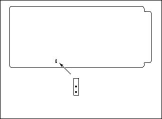
Figure 2. P1 Switch Location
|
|
|
Table 4. Front Panel Indicators and Switches |
|
Indicators |
Description |
|
|
|
|
|
|
DSL ........................ |
Indicates four possible states of the quality of the DSL signal. (The signal quality has a provisionable |
|
|
|
threshold of |
2, 4, 6, or 8 dB above a 10-7 BER.) |
|
|
Off ......................... |
No synchronization of FT1 DP and FNID |
|
|
Yellow ................... |
Poor signal quality (below 2 dB above 10-7 BER) |
|
|
Green .................... |
Good signal quality (above 2 dB above 10-7 BER) |
|
|
Blinking ................ |
An error has been detected on the loop |
|
DS1 ......................... |
Indicates four possible conditions: |
|
|
|
Green .................... |
The customer-side DS1 signal is present and synchronized |
|
|
Yellow ................... |
Yellow alarm at customer side DS1 |
|
|
Off ......................... |
No customer-side DS1 signal present |
|
|
Blinking ................ |
An error has been detected at FNID input |
|
LB ........................... |
Indicates three possible loopback states: |
|
|
|
Off ......................... |
No active loopbacks |
|
|
Blinking ................ |
FNID or repeater is in loopback |
|
|
On (solid) ............. |
Local (FT1 DP) loopback is active |
|
SX ........................... |
Sealing current is present |
|
|
ALM ....................... |
Indicate alarm condition |
|
|
|
On ......................... |
Alarm condition detected either locally (FT1 DP) or remotely (FNID) |
|
|
Off ......................... |
No alarm condition detected |
|
AP ........................... |
This LED will be On when Hardware Provisioning does not match software provisioning. |
|
|
Rotary Switch ......... |
Selects number of DS0 channels. (See subsection 1 of this practice for a description of time slot allocation.) |
|
|
|
|
|
|
|
|
|
61245207L2-5C |
Section 61245207L2-5, Issue 2 |
5 |
3. CONNECTIONS
The FT1 DP occupies one card slot in a Nortel DE-4E shelf. Power signaling is provided to the card through the backplane of the channel bank. See Figure 3 for FT1 DP edge connector wiring.
|
|
|
|
|
|
|
|
|
|
|
|
|
|
|
|
|
|
|
|
|
|
|
|
|
|
|
|
|
|
|
|
|
|
|
|
|
|
A1 |
B1 |
|
|
||||||
|
|
|
|
|
|
|
|
|
|
|
|
|
|
A2 |
B2 |
|
|
||||||
|
|
|
|
|
|
|
|
|
|
|
|
|
|
A3 |
B3 |
|
|
||||||
|
|
|
|
|
|
|
|
|
|
|
|
|
|
A4 |
B4 |
|
|
||||||
|
|
|
|
|
|
|
|
|
|
|
|
|
|
A5 |
B5 |
|
|
||||||
5 V Ground |
|
|
|
|
|
A6 |
B6 |
|
|
||||||||||||||
|
|
|
|
|
|
||||||||||||||||||
5 V Ground |
|
|
|
|
A7 |
B7 |
|
|
|||||||||||||||
|
|
|
|
|
|
|
|
|
|
|
|
|
|
A8 |
B8 |
|
|
||||||
DS0 Channel Rx Signal |
|
|
|
|
|
|
A9 |
B9 |
|
|
|
|
|
DS0 Channel Tx Signal |
|||||||||
|
|
|
|
|
|
|
|
|
|
||||||||||||||
A-Bit Tx Signaling Bus |
|
|
|
|
|
A10 |
B10 |
|
|
|
|
B-Bit Tx Signaling Bus |
|||||||||||
DS0 Tx Bus Enable |
|
|
|
|
|
A11 |
B11 |
|
|
|
|
DS0 Rx Clock |
|||||||||||
|
|
|
|
|
|
|
|
||||||||||||||||
Signaling Bus Enable |
|
|
|
|
|
|
A12 |
B12 |
|
|
|
|
DS0 Tx Clock |
||||||||||
Rx Signaling Bus |
|
|
|
|
|
|
A13 |
B13 |
|
|
|
|
Carrier Group Alarm |
||||||||||
|
|
|
|
|
|
|
|
|
|||||||||||||||
A-Bit Rx Signaling Strobe |
|
|
|
|
A14 |
B14 |
|
|
|
B-Bit Rx Signaling Strobe |
|||||||||||||
Transmit PCM |
|
|
|
|
A15 |
B15 |
|
|
Receive PCM |
||||||||||||||
|
|
|
|
|
|
|
|
|
|
|
|
|
|
A16 |
B16 |
|
|
||||||
|
|
|
|
|
|
|
|
|
|
|
|
|
|
A17 |
B17 |
|
|
||||||
|
|
|
|
|
|
|
|
|
|
|
|
|
|
A18 |
B18 |
|
|
||||||
Frame Ground |
|
|
|
|
A19 |
B19 |
|
|
|||||||||||||||
|
|
|
|
|
|||||||||||||||||||
-48 V |
|
|
|
|
|
|
|
|
|
|
|
A20 |
B20 |
|
|
||||||||
|
|
|
|
|
|
|
|
|
|
|
|
||||||||||||
-48 V Return |
|
|
|
|
|
|
|
|
|
|
A21 |
B21 |
|
|
|||||||||
|
|
|
|
|
|
|
|
|
|
|
|||||||||||||
|
|
|
|
|
|
|
|
|
|
|
|
|
|
A22 |
B22 |
|
|
||||||
|
|
|
|
|
|
|
|
|
|
|
|
|
|
A23 |
B23 |
|
|
||||||
|
|
|
|
|
|
|
|
|
|
|
|
|
|
A24 |
B24 |
|
|
||||||
|
|
|
|
|
|
|
|
|
|
|
|
|
|
A25 |
B25 |
|
|
||||||
|
|
|
|
|
|
|
|
|
|
|
|
|
|
A26 |
B26 |
|
|
||||||
DS0 Bit Clock |
|
|
|
A27 |
B27 |
|
|
||||||||||||||||
|
|
|
|
|
|||||||||||||||||||
|
|
|
|
|
|
|
|
|
|
|
|
|
|
A28 |
B28 |
|
|
||||||
|
|
|
|
|
|
|
|
|
|
|
|
|
|
A29 |
B29 |
|
|
||||||
|
|
|
|
|
|
|
|
|
|
|
|
|
|
A30 |
B30 |
|
|
||||||
|
|
|
|
|
|
|
|
|
|
|
|
|
|
A31 |
B31 |
|
|
||||||
|
|
|
|
|
|
|
|
|
|
|
|
|
|
A32 |
B32 |
|
|
DS0 Byte Clock |
|||||
|
|
|
|
|
|
|
|
|
|
|
|
|
|
A33 |
B33 |
|
|
||||||
HDSL Ring |
|
|
|
|
A34 |
B34 |
|
|
|||||||||||||||
|
|
|
|
|
|||||||||||||||||||
+5 V |
|
|
|
|
A35 |
B35 |
|
|
HDSL Tip |
||||||||||||||
|
|
|
|
|
|||||||||||||||||||
|
|
|
|
|
|
|
|
|
|
|
|
|
|
|
|
|
|
|
|
|
|
|
|
|
|
|
|
|
|
|
|
|
|
|
|
|
|
|
|
|
|
|
|
|
|
|
|
level problems that may occur at installation or during operation of the FT1 HDSL system. The following subsections describe additional testing features conducted with the front panel Bantam jacks as well as other faceplate features.
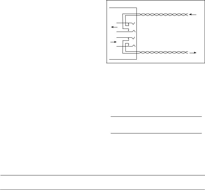
Bantam Jack Description
The front panel of the FT1 DP contains DS0 splitting Bantam jacks. The metallic splitting jacks provide an intrusive, signal interrupting access to the first DS0 channel. It is very important to know the direction of the access provided by a metallic splitting jack. Detailed descriptions of the FT1 DP Bantam jacks are given in the following subsection. Figure 4 shows the Bantam jack arrangement and details for specific jacks.
FT1 DP
|
TX |
Channel Bank |
|
DS0 Interface 1 |
|
|
Interface |
|
|
||
|
Logic Level - NEAR |
|
|
RX |
|
|
|
|
|
|
|
Figure 4. Bantam Jack Arrangement
FT1 DP Bantam Jacks
The FT1 DP provides a set of dual Bantam jacks on the front panel. These Bantam jacks allow connection of a Tele-Path Instruments 108/109 RT II (or equivalent) test set through one DS0 channel at
64 kbps for functions such as sending and receiving bit error rate signals.
NOTE
The DS0 access jacks are logic level interface.
Figure 3. FT1 DP Edge Connector Wiring
4. DSL SYSTEM TESTING
The ADTRAN DSL system provides extensive ability to monitor the status and performance of the DS1 signals and DSL loop signals. These features are valuable in troubleshooting and isolating any system
FT1 DP Loopbacks
There are two loopbacks available to the FT1 DP. FT1 DP network loopback loops the FT1 signal back to the network. The FT1 DP CPE loopback loops the FT1 signal back to the customer. The FT1 system loopback capabilities are described in detail in Appendix A of this practice.
1Logic level NEAR loopback on the DS0 interface is toward the outside cable pair. The FT1 DP will support logic level FAR loopback only in the presence of a BERT or loopback on the network end of the channel bank.
6 |
Section 61245207L2-5, Issue 3 |
61245207L2-5C |
 Loading...