

Page 1
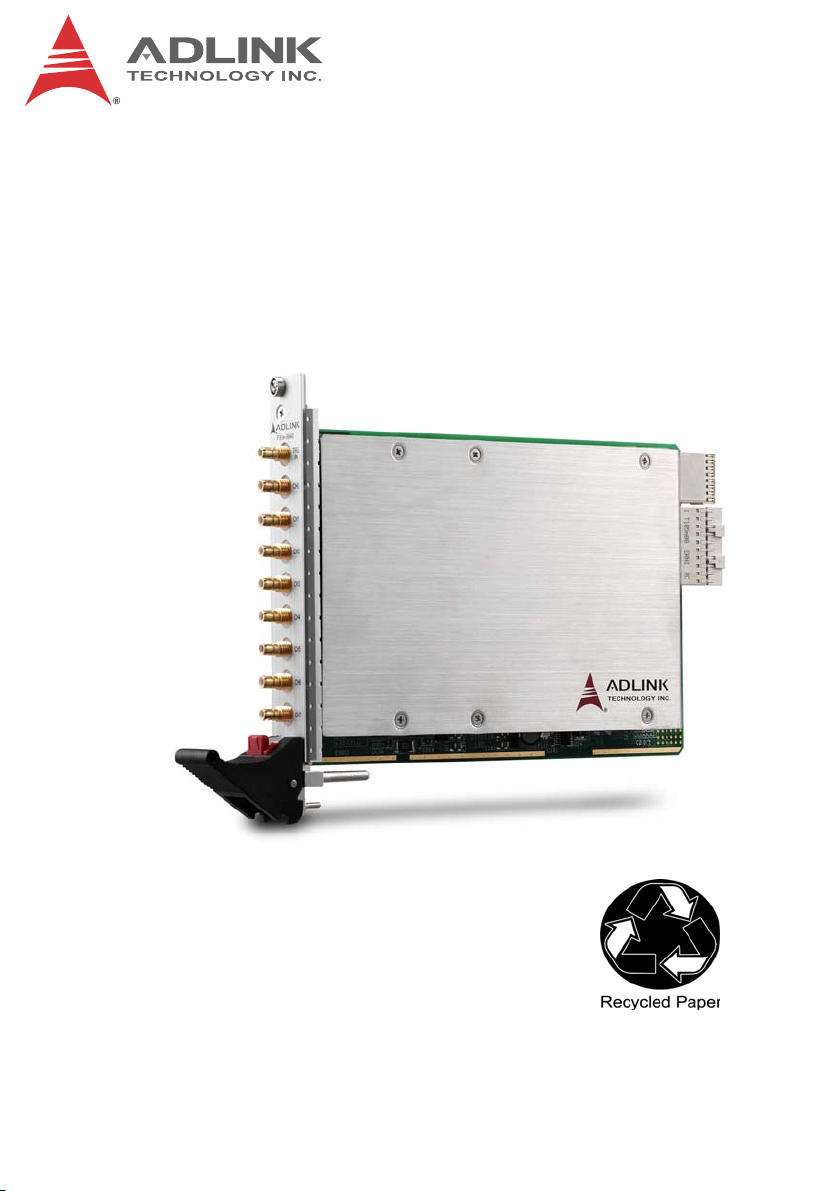
PXIe-9848
8-CH 14Bit 100 MS/s High-Speed PXI Express
Digitizer
User’s Manual
Manual Rev.: 2.01
Revision Date: Jan. 15, 2013
Part No: 50-17040-1010
Advance Technologies; Automate the World.
Page 2

Revision History
Revision Release Date Description of Change(s)
2.00 2012/10/26 Initial Release
2.01 2013/01/15 Graphic labeling corrected
ii
Page 3

PXIe-9848
Preface
Copyright 2013 ADLINK Technology, Inc.
This document contains proprietary information protected by copyright. All rights are reserved. No part of this manual may be reproduced by any mechanical, electronic, or other means in any form
without prior written permission of the manufacturer.
Disclaimer
The information in this document is subject to change without prior
notice in order to improve reliability, design, and function and does
not represent a commitment on the part of the manufacturer.
In no event will the manufacturer be liable for direct, indirect,
special, incidental, or consequential damages arising out of the
use or inability to use the product or documentation, even if
advised of the possibility of such damages.
Environmental Responsibility
ADLINK is committed to fulfill its social responsibility to global
environmental preservation through compliance with the European Union's Restriction of Hazardous Substances (RoHS) directive and Waste Electrical and Electronic Equipment (WEEE)
directive. Environmental protection is a top priority for ADLINK.
We have enforced measures to ensure that our products, manufacturing processes, components, and raw materials have as little
impact on the environment as possible. When products are at their
end of life, our customers are encouraged to dispose of them in
accordance with the product disposal and/or recovery programs
prescribed by their nation or company.
Conventions
Take note of the following conventions used throughout this
manual to make sure that users perform certain tasks and
instructions properly.
Preface iii
Page 4
NOTE:
NOTE:
CAUTION:
WARNING:
Additional information, aids, and tips that help users perform
tasks.
Information to prevent minor physical injury, component damage, data loss, and/or program corruption when trying to complete a task.
Information to prevent serious physical injury, component
damage, data loss, and/or program corruption when trying to
complete a specific task.
iv Preface
Page 5

PXIe-9848
Table of Contents
Preface .................................................................................... iii
List of Figures ....................................................................... vii
List of Tables.......................................................................... ix
1 Introduction ........................................................................ 1
1.1 Features............................................................................... 1
1.2 Applications ......................................................................... 2
1.3 Specifications....................................................................... 2
1.3.1 Analog Input ............................................................... 2
1.3.2 Timebase....................................................................3
1.3.3 Triggers ...................................................................... 4
1.3.4 General Specifications................................................ 4
1.4 Software Support ................................................................. 5
1.4.1 SDK ............................................................................ 5
1.4.2 WD-DASK................................................................... 6
1.5 Device Layout and I/O Array................................................ 7
2 ................................................................... Getting Started 9
2.1 Installation Environment ...................................................... 9
2.2 Installing the module.......................................................... 10
3 Operations ........................................................................ 13
3.1 Functional Block Diagram.................................................. 13
3.2 Analog Input Channel ........................................................ 13
3.2.1 Analog Input Front-End Configuration ...................... 13
3.2.2 Input Range and Data Format .................................. 15
3.2.3 FIFO and DMA Transfer For Analog Input ............... 16
3.3 Trigger Source and Trigger Modes.................................... 18
3.3.1 Trigger Sources ........................................................ 18
Table of Contents v
Page 6

3.4 Trigger Modes.................................................................... 22
3.4.1 Post Trigger Mode .................................................... 23
3.4.2 Pre-trigger Mode....................................................... 23
3.4.3 Middle-trigger Mode.................................................. 24
3.4.4 Delayed Trigger Mode .............................................. 24
3.4.5 Post-Trigger or Delayed-Trigger Acquisition with Re-Trig-
gering........................................................................ 25
3.5 ADC Timing Control ........................................................... 25
3.5.1 Timebase Architecture.............................................. 25
3.5.2 Basic Acquisition Timing........................................... 26
4 Calibration ........................................................................ 29
4.1 Calibration Constant .......................................................... 29
4.2 Auto-Calibration ................................................................. 29
Important Safety Instructions.............................................. 31
Getting Service ..................................................................... 33
vi Table of Contents
Page 7

PXIe-9848
List of Figures
Figure 1-1: Analog Input Channel Bandwidth, ±2 V Input Range
20MHz3
Figure 1-2: Analog Input Channel Bandwidth, ±2 V Input Range
100MHz3
Figure 1-3: PXIe-9848 Dimensions...............................................7
Figure 1-4: PXIe-9848 I/O Array ................................................... 8
Figure 3-1: Analog Input Architecture of the PXIe-9848 ............. 13
Figure 3-2: Linked List of PCI Address DMA Descriptors ........... 17
Figure 3-3: Trigger Architecture of the PXIe-9848 ...................... 18
Figure 3-4: External Digital Trigger ............................................. 19
Figure 3-5: External Digital Trigger Configuration....................... 20
Figure 3-6: Analog Trigger Conditions ........................................ 21
Figure 3-7: Post-Trigger Acquisition ........................................... 23
Figure 3-8: Pre-trigger Acquisition .............................................. 23
Figure 3-9: Middle-trigger Acquisition ......................................... 24
Figure 3-10: Delayed Trigger Mode Acquisition............................ 24
Figure 3-11: Re-Trigger Mode Acquisition .................................... 25
Figure 3-12: PXIe-9848 Timebase Architecture............................ 25
Figure 3-13: Basic Digitizer Acquisition Timing............................. 27
Figure 3-14: Varying Sampling Rates by Adjusting Scan Interval
Counter27
List of Figures vii
Page 8

This page intentionally left blank.
viii List of Figures
Page 9

PXIe-9848
List of Tables
Table 1-1: Channel Characteristics................................................... 2
Table 1-2: Analog Input Bandwidth................................................... 2
Table 1-3: Timebase......................................................................... 3
Table 1-4: Trigger Source & Mode.................................................... 4
Table 1-5: Digital Trigger Input .........................................................4
Table 1-6: PXIe-9848 I/O Array ........................................................8
Table 3-1: Input Range and Data Format ....................................... 15
Table 3-2: Input Range FSR and –FSR Values.............................. 15
Table 3-3: Input Range Midscale Values........................................ 15
Table 3-4: Ideal Transfer Characteristics for Analog Triggers ........ 22
Table 3-5: Counter Parameters and Description ............................28
List of Tables ix
Page 10

This page intentionally left blank.
x List of Tables
Page 11

1 Introduction
The PXIe-9848 high-speed 8CH 14-bit 100 MS/s digitizer is specifically designed for applications such as PSU (power supply unit)
testing, LIDAR testing, and radar signal acquisition. Analog inputs
with 100 MHz bandwidth can receive ±2V high-speed signals with
50 impedance. With a simplified front-end design and highly stable onboard reference, the PXIe-9848 provides not only highly
accurate measurement results but also superior dynamic performance.
For applications requiring real-time data acquisition and transfer,
PXIe-9848 is based on the PXI Express x4 bus interface. When
signals are converted from analog to digital, data is continuously
transferred to host system memory thanks to maximized PCI
Express bandwidth.
PXIe-9848's auto-calibration is performed with onboard reference
circuitry that calibrates the offset and gain errors of analog input.
Once complete, the calibration constant is stored in EEPROM, to
be loaded and used as needed by the board. Because all calibration is executed automatically by software command, no manual
calibration of the module is required.
PXIe-9848
1.1 Features
X PXI Express hardware specification Rev. 1.0 compliant
X Up to 100 MS/s sampling rate
X High resolution 14-Bit ADC
X 100 MHz bandwidth for analog input
X 512 MB onboard storage memory
X Scatter-Gather DMA data transfer for high-speed data
streaming
X One external digital trigger input
X Full auto-calibration
Introduction 1
Page 12
1.2 Applications
X Radar signal acquisition
X IF signal spectrum monitoring
X Optical fiber testing
X Power supply unit (PSU) testing
X Cable fault location and partial discharge monitoring for
power applications
1.3 Specifications
1.3.1 Analog Input
Channel Characteristics
Channels 8 single-ended channels
Connector type SMB screw type
Input coupling AC or DC, software selectable
ADC resolution 14-Bit
Input signal range ±2.0 V or ±0.2 V
Overvoltage ±5 V
Input impedance 50 or 1 M, software selectable
Offset error ±1 mV
Gain error ±0.5%
Table 1-1: Channel Characteristics
Analog Input Bandwidth (-3 dB)
±2.0 V input 100 MHz or 20 MHz, software selectable
Table 1-2: Analog Input Bandwidth
2 Introduction
Page 13

PXIe-9848
Figure 1-1: Analog Input Channel Bandwidth, ±2 V Input Range 20MHz
Figure 1-2: Analog Input Channel Bandwidth, ±2 V Input Range 100MHz
1.3.2 Timebase
Sample clock source Internal: onboard clock (oscillator)
Sample clock source Internal: onboard clock (oscillator)
External: PXI_CLK10, PXIe_CLK100
Timebase frequency 100 MHz
Sampling rate 100 MS/s ~ 1025.9 S/s
Internal Timebase Accuracy
Table 1-3: Timebase
Introduction 3
< s25 ppm
Page 14
1.3.3 Triggers
Trigger Source & Mode
Software command, external digital trigger, analog
Trigger source
Trigger mode
Digital Trigger Input
Sources Front panel SMB connector
Configurable threshold 0.8 mV ~ 3.3 V, default 1.67 V
Adjustable step 0.8 mV, 3.3 V with 12-bit resolution
Maximum input overload -0.5 V ~ +5.5 V
Trigger polarity Rising or falling edge
Pulse width 20 ns minimum
inputs, PXI trigger bus [0..7], and PXIe_DSTARB and
PXI_STAR
Post-trigger, pre-trigger, middle trigger, and delay trigger,
re-trigger for all trigger modes
Table 1-4: Trigger Source & Mode
Table 1-5: Digital Trigger Input
1.3.4 General Specifications
Specifications
Physical dimensions 160 W x 100 H mm (6.3 x 3.94 in.)
Bus
Bus interface PXI Express, PXI hybrid compatible
PCIe signaling PCI Express x 4, Gen 1
Environmental toleance
Operating Temperature: 0°C - 50°C
Relative humidity: 5% - 95%, non-condensing
Storage Temperature: -20°C - +80°C
Relative humidity: 5% - 95%, non-condensing
4 Introduction
Page 15

PXIe-9848
Calibration
Onboard reference +2.5 V
Temperature coefficient ±5 ppm/°C
Warm-up time 15 minutes
Power Consumption
Power Rail Standby Current (mA) Full Load (mA)
+3.3 V 5350 5900
+12 V 470 500
1.4 Software Support
ADLINK provides versatile software drivers and packages to suit
various user approaches to building a system. Aside from programming libraries, such as DLLs, for most Windows-based systems, ADLINK also provides drivers for other application
environments such as LabVIEW®.
All software options are included in the ADLINK All-in-One CD.
Commercial software drivers are protected with licensing codes.
Without the code, you may install and run the demo version for
trial/demonstration purposes for only up to two hours. Contact
your ADLINK dealer to purchase the software license.
1.4.1 SDK
For customers who want to write their own programs, ADLINK provides the following software development kits.
Z DAQPilot for Windows, compatible with various applica-
tion environments, such as VB.NET, VC.NET, VB/VC++,
BCB, and Delphi
Z DAQPilot for LabVIEW
Z Toolbox adapter for MATLAB
Introduction 5
Page 16

1.4.2 WD-DASK
WD-DASK includes device drivers and DLL for Windows 2000/
XP/Vista/7. DLL is binary compatible across Windows
2000/XP/ Vista/7. This means all applications developed with
WD-DASK are compatible with these Windows operating systems.
The devel- opment environment may be VB, VB.NET, VC++, BCB,
and Delphi, or any Windows programming language that
allows calls to a DLL. The WD-DASK user and function reference
manu- als are on the ADLINK All-in-One CD.
6 Introduction
Page 17

1.5 Device Layout and I/O Array
All dimensions are in mm
NOTE:
NOTE:
165.04
162.54
PXIe-9848
100
210.032
Figure 1-3: PXIe-9848 Dimensions
The PXIe-9848 I/O array is labeled to indicate connectivity, as
shown.
Introduction 7
Page 18

Figure 1-4: PXIe-9848 I/O Array
Name
Ext. Digital Trigger
Input
Analog Input
Channel (x8)
8 Introduction
Faceplate
Legend
TRG IN
CH0 to
CH7
Table 1-6: PXIe-9848 I/O Array
Type Remark
External digital trigger input,
receiving trigger signal from
SMB
screw
type
external instrument and
initiating acquisition
Analog input channel
Page 19

2 Getting Started
This chapter describes proper installation environment, installation
procedures, package contents and basic information users should
be aware of regarding the PXIe-9848.
Diagrams and illustrated equipment are for reference only.
Actual system configuration and specifications may vary.
NOTE:
NOTE:
2.1 Installation Environment
When unpacking and preparing to install, please refer to Important
Safety Instructions.
Only install equipment in well-lit areas on flat, sturdy surfaces with
access to basic tools such as flat- and cross-head screwdrivers,
preferably with magnetic heads as screws and standoffs are small
and easily misplaced.
Recommended Installation Tools
X Phillips (cross-head) screwdriver
X Flat-head screwdriver
X Anti-static wrist strap
X Antistatic mat
ADLINK PXIe-9848 DAQ modules are electrostatically sensitive
and can be easily damaged by static electricity. The module must
be handled on a grounded anti-static mat. The operator must wear
an anti-static wristband, grounded at the same point as the
anti-static mat.
PXIe-9848
Getting Started 9
Page 20

Inspect the carton and packaging for damage. Shipping and handling could cause damage to the equipment inside. Make sure that
the equipment and its associated components have no damage
before installation.
The equipment must be protected from static discharge and
physical shock. Never remove any of the socketed parts except
CAUTION:
at a static-free workstation. Use the anti-static bag shipped with
the product to handle the equipment and wear a grounded
wrist strap when servicing.
X Package Contents
X PXIe-9848 high-speed digitizer
X ADLINK All-in-one compact disc
X PXIe-9848 User’s Manual
If any of these items are missing or damaged, contact the dealer
Do not install or apply power to equipment that is damaged or
missing components. Retain the shipping carton and packing
WARNING:
materials for inspection. Please contact your ADLINK
dealer/vendor immediately for assistance and obtain authorization before returning any product.
2.2 Installing the module
1. Turn off the PXI system/chassis and connect the power
cable from the power source.
Connection of the power cable provides grounding to prevent
hazardous ESD (electrostatic discharge).
NOTE:
NOTE:
2. Align the module’s edge with the module guide in the
PXI chassis.
3. Slide the module into the chassis until resistance is felt
from the PXI connector.
4. Push the ejector latch upwards and fully insert the module into the chassis.
10 Getting Started
Page 21

5. Once the module is fully seated, a “click” can be heard
from the ejector latch.
6. Tighten the screw on the front panel.
7. Power up the PXI system/chassis.
The red ejector latch lock must be depressed before the module can be uninstsalled.
NOTE:
NOTE:
PXIe-9848
Getting Started 11
Page 22

This page intentionally left blank.
12 Getting Started
Page 23

3 Operations
This chapter contains information regarding analog input, analog
output, triggering and timing for the PXIe-9848, as well as data
transfer and multiple module synchronization functions.
3.1 Functional Block Diagram
Quad
CH0
CH1
CH2
CH3
CH4
CH5
CH6
CH7
TRG IN
JFET OP
Buffer
BUF VGA
BUF VGA
BUF VGA
BUF VGA
Reference &
Calibration
BUF VGA
BUF VGA
BUF VGA
BUF VGA
Input
Control
High Speed
VGA
High Speed
VGA
ADC
ADC
ADC
ADC
ADC
ADC
ADC
ADC
14bit 100MSps
ADC
Quad
14bit 100MSps
ADC
8-bit / 200MHz
PLL CLK
Synthesizer
8-bit / 200MHz
DC-DC\
LDO
PXI_CLK10
Geographical Address [0..4]
Trigger Bus [0..7]
PXI_STAR
PXIe_CLK100
FPGA
ADC Control
Trigger Control
DDR2
512MB
Memory
PXIe_DSTARBp/n
3.3V
5V
12V
SPI
10 MHz
CLK100p/n
PXI CLK10
SPI
3.3V
5V
12V
PCIe Controller
ADC
BUS
Data Processing
Board to Board Conn x2
PXIe-9848
XJ4
PCIe Gen1
XJ3
x4
PXIe Hybrid Peripheral Slot
3.2 Analog Input Channel
3.2.1 Analog Input Front-End Configuration
Relay Relay
CH0
50ohm
Figure 3-1: Analog Input Architecture of the PXIe-9848
Operations 13
1Gohm
Relay
1Mohm
P
O
T
E
r
F
e
f
J
f
u
B
d
e
e
p
S
h
g
A
i
G
H
V
Relay
+2.5V
Reference
&
Calibration
Quad
14bit 100MSps
ADC
CLK
GEN
AD9523
Board to Board Bus
10 MHz
Page 24

As shown, in the signal channel analog input path of a digitizer,
each path provides 50 input impedance or high impedance and
DC couple or AC couple. The gain amplifier is optimized for each
input range with low noise and high dynamic range. An anti-aliasing filter with a choice of 100MHz or 20MHz further eliminates high
frequency noise. The 14-bit ADC provides not only accurate DC
performance but also high signal-to-noise ratio and high non-spurious dynamic range.
For auto-calibration, internal calibration provides stable and accurate reference voltage to the AI.
Input Impedance Configuration
When acquiring high frequency signals (of at least MHz frequency), to prevent reflection from the line, set “Characteristic
Impedance” to equal 50 from the signal source, such as a
high speed function generator, transmission line, such as a
coaxial cable, to the digitizer input. For this application, 50
impedance switch is provided, matching the Characteristic
Impedance from the connector, PCB trace and input of the gain
amplifier equaling 50.
If the signal source is not terminated with low impedance and
the transmission line is short, PXIe-9848 provides overall high
impedance of 1M.
AC and DC Input Coupling
With DC coupling, DC offset present in the input signal is
passed to ADC, and is indicated if the signal source has a low
level of offset voltage or if DC content of the signal is important.
In AC coupling, the DC offset present in the input signal
is erased, and is indicated if the DC content of the input signals
is to be rejected. AC coupling enables a high pass R-C filter
through the input signal path. Corner frequency (-3dB) is about
10Hz.
100MHz and 20MHz Bandwidth
For applications that require lower bandwidth for low frequency
input signals, PXIe-9848 provides a bandwidth limit of 20MHz
to eliminate high frequency noise and raise the SNR ratio.
14 Operations
Page 25

PXIe-9848
3.2.2 Input Range and Data Format
A/D acquisition is initiated by a trigger source, which must be pre-
determined. Data acquisition will commence once the trigger condition is established. Following completion of A/D conversion, A/D
data is buffered in a Data FIFO, and can then be transferred to PC
memory for further processing.
Data format of the PXIe-9848 is 2’s complement. The ADC data of
the PXIe-9848 is on the 14 MSB of the 16-bit A/D data. The 2 LSB
of the 16-bit A/D data should be truncated by software. A/D data
structure is as follows.
D15 D14 D13 D12 …. D3 D2 D1 D0
D15 ~ D2 bits represent the data from ADC CHx (2’s complement)
D1, D0 bits are identical to D2 bit and should be truncated.
Table 3-1: Input Range and Data Format
Description
Bipolar
Analog Input
Digital Code N/A N/A 7FFF 8000
Description Midscale +1LSB Midscale Midscale –1LSB
Bipolar
Analog Input
Digital Code 0001 0000 FFFF
Full-scale
range
±2 V 244.14 V 1.999756 V -2 V
±0.2V 24.41 V 0.199975 V -0.2 V
Table 3-2: Input Range FSR and –FSR Values
244µV 0 V -244µV
24.41 V 0 V -24.41 V
Table 3-3: Input Range Midscale Values
Least
significant
bit
FSR-1LSB -FSR
Operations 15
Page 26

3.2.3 FIFO and DMA Transfer For Analog Input
FIFO
One FIFO is implemented on the PXIe-9848 for analog input
data storage. FIFO depth is 32M samples/ per channel and is not
shared between all AI channels.
Bus-Mastering DMA Data Transfer
PCI Express offers dedicated bandwidth of up to 250MB/s. Unlike
the PCI bus, having parallel bus architecture dividing bandwidth
among all devices on the bus, PCI Express features peer-to-peer
architecture with dedicated data pipelining. Data can be transferred at 2.5Gb/s, which enables a theoretical 250MB/s bandwidth
per lane. With PCI Express, data bandwidth is dramatically
improved compared to the PCI bus, allowing data to be streamed
to the system faster with minimum onboard memory required.
One of the most important features of the PXIe-9848 is the PCI
Express Gen 1 x 4 interface. The PXIe-9848 is equipped with eight
100MS/s high sampling rate ADCs, generating data rates up to 1.6
GByte/s. When streaming this data from ADCs to system memory,
bandwidth remains insufficient. Data bandwidth is 1.6 GByte/s
while the PCI Express Gen 1 X4 is only up to 1 GByte/s. Reducing
the number of acquired channels or decreasing the sampling rate
enables unlimited streaming, making it useful to have a high bandwidth bus interface when streaming data from ADC to system
memory.
Actual data throughput for a PC system depends on system topology, data transfer between other devices in the system, and other
components in the system. For example, data transfer between
digitizers and host memory usually travels through a PCIe switch
before transfer to the host system. All digitizers share the bandwidth available on the link between PCIe switch and the host system.
To provide efficient data transfer, a PCI bus-mastering DMA is
essential for continuous data streaming, as it helps to achieve full
potential PCI Express bus bandwidth. The bus-mastering controller releases the burden on the host CPU since data is directly
16 Operations
Page 27

PXIe-9848
transferred to the host memory without intervention. Once analog
input operation begins, the DMA returns control of the program.
During DMA transfer, the hardware temporarily stores acquired
data in the onboard AD Data FIFO, and then transfers the data to
a user-defined DMA buffer in the computer.
Using a high-level programming library for high speed DMA data
acquisition, the sampling period and the number of conversions
needs simply to be assigned into specified counters. After the AD
trigger condition is met, the data will be transferred to the system
memory by the bus-mastering DMA.
In a multi-user or multi-tasking OS, such as Microsoft Windows,
Linux, or other, it is difficult to allocate a large continuous memory
block. Therefore, the bus controller provides DMA transfer with
scatter-gather function to link non-contiguous memory blocks into
a linked list enabling transfer of large amounts of data without
memory limitations. In non-scatter-gather mode, the maximum
DMA data transfer size is 2 MB double words (8 MB bytes); in
scatter-gather mode, there is no limitation on DMA data transfer
size aside from the physical storage capacity of the system.
Users can also link descriptor nodes circularly to achieve a multibuffered DMA. In the following linked list, comprising three DMA
descriptors, each descriptor contains a PCI address, PCI dual
address, transfer size, and pointer to the next descriptor.
PCI address and PCI dual address support 64-bit addresses
which can be mapped into more than 4 GB of address space.
First PCI Address
First Dual Address
Transfer Size
Next Descriptor
PCI Address
Dual Address
Transfer Size
Next Descriptor
PCI Express Bus
Local Memory
(FIFO)
PCI Address
Dual Address
Transfer Size
Next Descriptor
Figure 3-2: Linked List of PCI Address DMA Descriptors
Operations 17
Page 28

3.3 Trigger Source and Trigger Modes
This section details PXIe-9848 triggering operations. All eight AI
channels share the same trigger source. Each of five types of trigger source cooperates with five trigger modes to accommodate
various data acquisition applications. For more details on programming the PXIe-9848, please refer to the software operation manual.
3.3.1 Trigger Sources
Analog CH0
Analog CH1
Analog CH2
Analog CH3
Analog CH4
Analog CH5
Analog CH6
Analog CH7
TRG IN
SMB Connector
Analog
Trigger
Selection
PXI Interface
Software Trigger
Digital Trigger Input
Analog
Trigger
PXI_STAR
PXIe_DSTARB
PXI Trigger Bus[0:7]
Trigger Source Mux
Trigger
Decision
To Internal
Circuit
SSI_TRIG1
SSI_TRIG2
SSI_START_OP
PXI Trigger
Bus[0:7]
Trigger Output Mux
Figure 3-3: Trigger Architecture of the PXIe-9848
The PXIe-9848 requires a trigger to implement acquisition of data.
Configuration of triggers requires identification of trigger
source. The PXIe-9848 supports internal software trigger,
external digital trigger, PXI_STAR trigger, PXI Express STAR trigger (PXIe_DSTARB), and PXI Trigger Bus [0.7].
Software Trigger
The software trigger, generated by software command, is
asserted immediately following execution of specified function
calls to begin the operation.
PXI Interface
18 Operations
Page 29

PXIe-9848
External Digital Trigger
An external digital trigger is generated when a TTL edge or equiv-
alent wave slope is detected at the SMB connector on the front
panel. As shown, trigger polarity can be selected by software.
Note that minimum TTL pulse width is 20 ns and maximum input
wave frequency is 25 MHz.
Pulse Width > 20ns
Pulse Width > 20ns
Rising Edge Trigger Event Falling Edge Trigger Event
Figure 3-4: External Digital Trigger
Signal level of the external digital trigger signal can be configured
by onboard potentiometer as follows. The adjustable range is
0.8mV to 3.3V and the adjustable step 0.8mV (3.3V with 12bit resolution). The default voltage level is 1.67V.
Operations 19
Page 30

Protection Circuit
OR
Trigger IN
High Speed
3.3VDC
Trigger Threshold
Adjustment
Figure 3-5: External Digital Trigger Configuration
Comparator
PXI STAR Trigger
When PXI STAR is selected as the trigger source, the
PXIe-9848 accepts a TTL-compatible digital signal as a trigger signal. Triggering occurs when a rising edge or falling edge is
detected at PXI STAR, with trigger polarity configurable by software. The minimum pulse width requirement of this digital trigger
signal is 20 ns.
PXIe_DSTARB Trigger
The PXIe_DSTARB signal, a differential signal transmitted via the
PXI Express Chassis backplane, distributes high-speed,
high-quality trigger signals. When PXIe_DSTARB is selected as
the trigger source, the PXIe-9848 accepts a fast-switching LVDS
digital signal as a trigger signal. Triggering occurs when a rising
edge or falling edge is detected at PXIe_DSTARB, with trigger
polarity configurable by software, with minimum pulse width
requirement of 20 ns.
PXI Trigger Bus
The PXIe-9848 utilizes PXI Trigger Bus Numbers 0 through 7 to
act as a System Synchronization Interface (SSI). With the interconnected bus provided by PXI Trigger Bus, multiple modules are
easily synched. When configured as input, the PXIe-9848
serves as a slave module and can accept trigger signals from one
of buses 0 through 7. When configured as output, the PXIe-9848
20 Operations
Page 31

PXIe-9848
serves as a master module and can output trigger signals to the
PXI Trigger Bus Numbers 0 through 7.
Analog Trigger
PXIe-9848 analog trigger circuitry can be configured to monitor
one analog input channel from which data is acquired. Selection of
an analog input channel as the analog trigger channel does not
influence input channel acquisition. The analog trigger circuit generates an internal digital trigger signal based on the condition
between the analog signal and the defined trigger level.
Analog trigger conditions are either positive-slope trigger, in which
the trigger event occurs when the analog input signal changes
from a voltage lower than the specified trigger level to a voltage
exceeding the specified trigger level, or negative-slope trigger, in
which the trigger event occurs when the analog input signal
changes from a voltage exceeding the specified trigger level to a
voltage lower than the specified trigger level.
Positive-Slope Trigger Event
Occurs
Trigger Level
Analog
Signal
Figure 3-6: Analog Trigger Conditions
Negative-Slope Trigger
Event Occurs
The trigger signal can be chosen from among CH0, CH1, CH2,
CH3, CH4, CH5, CH6 and CH7 while using an external analog
Operations 21
Page 32

trigger source. The trigger level can be set by software with 14-bit
resolution, with characteristics as follows.
Trigger Level
Setting (Hex)
7FFF 1.999756V 0.199975V
7FFE 1.999512V 0.199951V
1 244.14uV 24.41uV
00V0V
FFFF -244.14uV -24.41uV
8001 -1.999756V -0.199975V
8000 -2V -0.2V
Table 3-4: Ideal Transfer Characteristics for Analog Triggers
Trigger Voltage
(-2V to +2V)
Trigger Voltage
(-0.2V to +0.2V)
Trigger Export
The PXIe-9848 can export trigger signals to PXI Trigger Bus Numbers 0 through 7. The Trigger Bus can be programmed to output
the trigger signal when the trigger source is generated by software, PXI STAR, or PXI Trigger Bus Numbers 0 through 7. The
PXIe-9848 utilizes PXI Trigger Bus Numbers 0 through 7 to act as
the System Synchronization Interface. When configured as the
output, the PXIe-9848 serves as a master module and can output
trigger signals to synchronize the slave modules. The trigger signal can be routed to any of the seven PXI Trigger Bus Numbers
via software.
3.4 Trigger Modes
Two trigger modes applied to trigger sources initiate different data
acquisition timings when a trigger event occurs. The following trigger mode descriptions are applied to analog input and analog output functions.
22 Operations
Page 33

PXIe-9848
3.4.1 Post Trigger Mode
Post-trigger acquisition is applicable when data is to be collected
after the trigger event, as shown. When the operation starts,
PXIe-9848 waits for a trigger event. Once the trigger signal is
received, acquisition begins. Data is generated from ADC and
transferred to system memory continuously. The acquisition stops
once the total data amount reaches a predefined value.
Trigger Ev ent Oc curs
Acqui sit ion st art
N samplesData
Acqui sit ion st op
Begin to transfer data to system
Trigger
Operation
start
Figure 3-7: Post-Trigger Acquisition
3.4.2 Pre-trigger Mode
Collects data before the trigger event, starting once specified function calls are executed to begin the pre-trigger operation, and
stopping when the trigger event occurs.If the trigger event occurs
after the specified amount of data has been acquired, the system
stores only data preceding the trigger event by a specified
amount, as follows.
Operation start
Acquisition start
Trigger
Data
X samples
X samples acquired
Despite acquired samples not reaching
N, acquisition stop and X samples in
memory are returned to system.
Trigger Event occurs
Acquisition stop
Data transfer to system begins
Specified amount of data,
(N samples)
Time
Time
Figure 3-8: Pre-trigger Acquisition
Operations 23
Page 34

3.4.3 Middle-trigger Mode
Used to collect data before and after the trigger event. The amount
of stored data before and after trigger event can be set individually
(M and N samples), as follows.
Operation start
Acquisition start
Trigger
Data
Trigger Event occurs
Acquisition stop
Data transfer to system begins
N samplesM samples
Figure 3-9: Middle-trigger Acquisition
Trigger events can only be accepted when the specified
amount of data has been acquired (M samples) since opera-
NOTE:
NOTE:
tion start. If the sampled data is insufficient, the trigger event
will be ignored.
3.4.4 Delayed Trigger Mode
Delayed-trigger acquisition is utilized to postpone data collection
after the trigger event, as shown. When PXIe-9848 receives a trigger event, a time delay is implemented before commencing acquisition. The delay is specified by a 16-bit counter value such that a
maximum thereof is the period of TIMEBASE X (232), and the minimum is the Timebase period.
Time
Figure 3-10: Delayed Trigger Mode Acquisition
24 Operations
Page 35

PXIe-9848
3.4.5 Post-Trigger or Delayed-Trigger Acquisition with Re-Triggering
Post-trigger or delayed trigger acquisition with re-triggering are
applicable to collect data after several trigger events, as shown.
Once the number of triggers has been programmed, the digitizer
acquires a specific data sample each time a trigger is accepted.
The time between a previous sample and subsequent trigger
event can only be one Timebase clock period. Following initial
setup, the process requires no additional software intervention.
Figure 3-11: Re-Trigger Mode Acquisition
3.5 ADC Timing Control
3.5.1 Timebase Architecture
VCXO
Onboard
Oscillator
10M
PXIe_CLK100
PXI_CLK10
PXIe Interface
Timebase Clock Switch
Figure 3-12: PXIe-9848 Timebase Architecture
The PXIe-9848 supports the following timebase sources for ana-
log input conversion.
Operations 25
100M
Multiplier
PLL
Synthesizer
ADC0
ADC1
Page 36

Internal Oscillator
The PXIe-9848 is equipped with a stable, low jitter reference oscillator for ADCs, at 10 MHz.
PXI_CLK10 Clock
The PXIe-9848 can receive the timebase from the PXI_CLK10
clock, the signal of which originates at the PXI Express chassis
backplane, matched in propagation delay within 1 ns.
PXIe_CLK100 Clock
The PXIe-9848 can receive the timebase from the PXIe_CLK100
clock, the signal of which originates at the PXI Express chassis
backplane, matched in propagation delay within 200 ps.
3.5.2 Basic Acquisition Timing
The PXIe-9848 commences acquisition upon receipt of a trigger
event originating with software command, external digital trigger,
or the PXI Trigger Bus. The Timebase is a clock provided to the
ADC and acquisition engine for essential timing. The Timebase is
from an onboard 100MHz oscillator. To achieve different sampling
rates, a scan interval counter is used.
Using the post-trigger mode as an example, as shown, when a
trigger is accepted by the digitizer, the acquisition engine commences acquisition of data from ADC, and stores the sampled
data to the onboard FIFO. When FIFO is not empty, data will be
transferred to system memory immediately through the DMA
engine. The sampled data is generated continuously at the rising
edge of Timebase according to the scan interval counter setting.
When sampled data reaches a specified value, in this example
256, acquisition ends.
26 Operations
Page 37

Analog
signal
TIMEBASE
Trigger
PXIe-9848
Acquisition
In Progress
DATA
Trigger mode = post-trigger, DataCnt = 256, ScanIntrv = 1
Acquisition starts right after this clock edge
D3 D4 D255
D2
D1
D253
D254
D256
Figure 3-13: Basic Digitizer Acquisition Timing
To achieve sampling rates other than 100MS/s, a number for scan
interval counter needs only be specified. For example, if the scan
interval counter is set as 2, the equivalent sampling rate is
100MS/s / 2 = 50MS/s. If as 3, the equivalent sampling rate is
100MS/s / 3 = 33.33MS/s, and vice versa. The scan interval counter is 16 bits in width, therefore the lowest sampling rate is
1.025KS/s (100MS/s / 65535).
Trigger
TIMEBASE
DATA
ScanIntrv = 1
ScanIntrv = 2
ScanIntrv = 3
Acquisition
In Progress
D2
D1
D1
D1
Acquisition is initiated following this clock edge
D4
D3
D2 D3 D4 D5 D6
D5
D2 D3 D4
D6
D8
D7
D10
D9
Figure 3-14: Varying Sampling Rates by Adjusting Scan Interval Counter
Operations 27
Page 38

Counter
Name
ScanIntrv 16-bit 1 - 65535 Timebase divider to achieve
DataCnt 32-bit 1 - 536870911 Specifies the amount of data to
trigDelayTicks 16-bit 1 -65535 Indicates time between a trigger
ReTrgCnt 32-bit 1 -536870911 Enables re-trigger to accept
Length Valid Value Description
equivalent sampling rate of the
digitizer, where Sampling rate =
Timebase / ScanIntrv
be acquired
event and commencement of
acquisition. The unit of a delay
count is the period of the
Timebase.
multiple triggers. Please see
Section 3.4.5: Post-Trigger or
Delayed-Trigger Acquisition with
Re-Triggering for more details.
Table 3-5: Counter Parameters and Description
28 Operations
Page 39

4 Calibration
This chapter introduces the calibration process to minimize analog
input measurement errors and analog output errors.
4.1 Calibration Constant
The PXIe-9848 is factory calibrated before shipment, with associ-
ated calibration constants written to the onboard EEPROM. At
system boot, the PXIe-9848 driver loads these calibration constants, such that analog input path and analog output circuit errors
are minimized. ADLINK provides a software API for calibrating the
PXIe-9848.
The onboard EEPROM provides three banks for calibration con-
stant storage. Bank 0, the default bank, records the factory calibrated constants, providing written protection preventing
erroneous auto-calibration. Bank 1 is user-defined space, provided for storage of self-calibration constants. Upon execution of
auto-calibration, the calibration constants are recorded to bank 1.
When PXIe-9848 boots, the driver accesses the calibration constants and is automatically set to hardware. The driver loads constants stored in bank 1 by default. Constants from bank 0 can be
loaded, with the preferred bank designated as boot bank by software. Following re-assignment of the bank, the driver will load the
desired constants on system re-boot. This setting is recorded to
EEPROM and is retained until re-configuration.
PXIe-9848
4.2 Auto-Calibration
Because errors in measurement and outputs will vary with time
and temperature, re-calibration is recommended when the module
is installed. Auto-calibration can measure and minimize errors
without external signal connections, reference voltages, or measurement devices.
The PXIe-9848 has an on-board calibration reference to ensure
the accuracy of auto-calibration. The reference voltage is measured on the production line and recorded in the on-board
EEPROM.
Calibration 29
Page 40

Before initializing auto-calibration, it is recommended to warm up
the PXIe-9848 for at least 20 minutes and remove connected
cables.
It is not necessary to manually factor delay into applications, as
the PXIe-9848 driver automatically adds the compensation
NOTE:
NOTE:
time.
30 Calibration
Page 41

PXIe-9848
Important Safety Instructions
For user safety, please read and follow all instructions,
WARNINGS, CAUTIONS, and NOTES marked in this manual and
on the associated equipment before handling/operating the
equipment.
X Read these safety instructions carefully.
X Keep this user’s manual for future reference.
X Read the specifications section of this manual for detailed
information on the operating environment of this equipment.
X When installing/mounting or uninstalling/removing
equipment:
Z Turn off power and unplug any power cords/cables.
X To avoid electrical shock and/or damage to equipment:
Z Keep equipment away from water or liquid sources;
Z Keep equipment away from high heat or high humidity;
Z Keep equipment properly ventilated (do not block or
cover ventilation openings);
Z Make sure to use recommended voltage and power
source settings;
Z Always install and operate equipment near an easily
accessible electrical socket-outlet;
Z Secure the power cord (do not place any object on/over
the power cord);
Z Only install/attach and operate equipment on stable
surfaces and/or recommended mountings; and,
Z If the equipment will not be used for long periods of time,
turn off and unplug the equipment from its power source.
Important Safety Instructions 31
Page 42

X Never attempt to fix the equipment. Equipment should only
be serviced by qualified personnel.
X A Lithium-type battery may be provided for uninterrupted,
backup or emergency power.
Risk of explosion if battery is replaced with an incorrect type;
please dispose of used batteries appropriately.
X Equipment must be serviced by authorized technicians
when:
Z The power cord or plug is damaged;
Z Liquid has penetrated the equipment;
Z It has been exposed to high humidity/moisture;
Z It is not functioning or does not function according to the
user’s manual;
Z It has been dropped and/or damaged; and/or,
Z It has an obvious sign of breakage.
32 Important Safety Instructions
Page 43

Getting Service
Contact us should you require any service or assistance.
ADLINK Technology, Inc.
Address: 9F, No.166 Jian Yi Road, Zhonghe District
New Taipei City 235, Taiwan
ᄅקؑխࡉ৬ԫሁ 166 ᇆ 9 ᑔ
Tel: +886-2-8226-5877
Fax: +886-2-8226-5717
Email: service@adlinktech.com
Ampro ADLINK Technology, Inc.
Address: 5215 Hellyer Avenue, #110, San Jose, CA 95138, USA
Tel: +1-408-360-0200
Toll Free: +1-800-966-5200 (USA only)
Fax: +1-408-360-0222
Email: info@adlinktech.com
ADLINK Technology (China) Co., Ltd.
Address: Ϟ⍋Ꮦ⌺ϰᮄᓴ∳催⾥ᡔು㢇䏃 300 ো(201203)
300 Fang Chun Rd., Zhangjiang Hi-Tech Park,
Pudong New Area, Shanghai, 201203 China
Tel: +86-21-5132-8988
Fax: +86-21-5132-3588
Email: market@adlinktech.com
ADLINK Technology Beijing
Address: ࣫ҀᏖ⍋⎔Ϟഄϰ䏃 1 োⲜ߯ࡼ E ᑻ 801 ᅸ(100085)
Rm. 801, Power Creative E, No. 1, B/D
Shang Di East Rd., Beijing, 100085 China
Tel: +86-10-5885-8666
Fax: +86-10-5885-8625
Email: market@adlinktech.com
PXIe-9848
ADLINK Technology Shenzhen
Address: ⏅ഇᏖቅ⾥ᡔು催ᮄϗ䘧᭄ᄫᡔᴃು
Tel: +86-755-2643-4858
Fax: +86-755-2664-6353
Email: market@adlinktech.com
ADLINK Technology (Europe) GmbH
Address: Nord Carree 3, 40477 Duesseldorf, Germany
Tel: +49-211-495-5552
Fax: +49-211-495-5557
Email: emea@adlinktech.com
A1 2 ὐ C (518057)
2F, C Block, Bldg. A1, Cyber-Tech Zone, Gao Xin Ave. Sec. 7,
High-Tech Industrial Park S., Shenzhen, 518054 China
Getting Service 33
Page 44

ADLINK Technology, Inc. (French Liaison Office)
Address: 15 rue Emile Baudot, 91300 Massy CEDEX, France
Tel: +33 (0) 1 60 12 35 66
Fax: +33 (0) 1 60 12 35 66
Email: france@adlinktech.com
ADLINK Technology Japan Corporation
Address: ͱ101-0045 ᵅҀ䛑ҷ⬄⼲⬄䤯ފ⬎ 3-7-4
Tel: +81-3-4455-3722
Fax: +81-3-5209-6013
Email: japan@adlinktech.com
ADLINK Technology, Inc. (Korean Liaison Office)
Address: 昢殾柢 昢爎割 昢爎壟 1675-12 微汾瘶捒娯 8猻
Tel: +82-2-2057-0565
Fax: +82-2-2057-0563
Email: korea@adlinktech.com
ADLINK Technology Singapore Pte. Ltd.
Address: 84 Genting Lane #07-02A, Cityneon Design Centre,
Tel: +65-6844-2261
Fax: +65-6844-2263
Email: singapore@adlinktech.com
ADLINK Technology Singapore Pte. Ltd. (Indian Liaison Office)
Address: 1st Floor, #50-56 (Between 16th/17th Cross) Margosa Plaza,
Tel: +91-80-65605817, +91-80-42246107
Fax: +91-80-23464606
Email: india@adlinktech.com
⼲⬄ 374 ɛɳ 4F
KANDA374 Bldg. 4F, 3-7-4 Kanda Kajicho,
Chiyoda-ku, Tokyo 101-0045, Japan
8F Mointer B/D,1675-12, Seocho-Dong, Seocho-Gu,
Seoul 137-070, Korea
Singapore 349584
Margosa Main Road, Malleswaram, Bangalore-560055, India
ADLINK Technology, Inc. (Israeli Liaison Office)
Address: 6 Hasadna St., Kfar Saba 44424, Israel
Tel: +972-9-7446541
Fax: +972-9-7446542
Email: israel@adlinktech.com
34 Getting Service
 Loading...