

Page 1
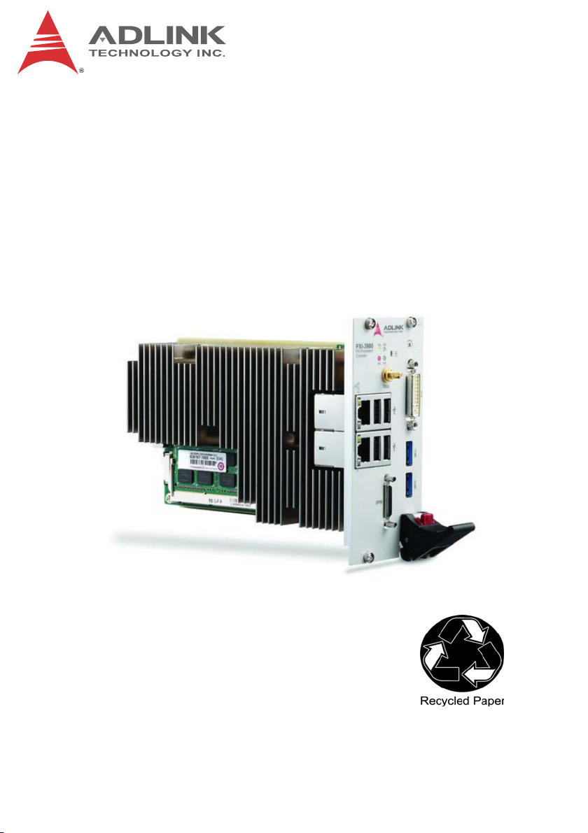
PXI-3980
PXI Embedded Controller
User’s Manual
Manual Rev.: 2.00
Revision Date: May 31, 2013
Part No: 50-17044-1000
Advance Technologies; Automate the World.
Page 2

Revision History
Revision Release Date Description of Change(s)
2.00 2013/5/31 Initial Release
ii
Page 3

PXI-3980
Preface
Copyright 2013 ADLINK TECHNOLOGY, INC.
This document contains proprietary information protected by copyright. All rights are reserved. No part of this manual may be reproduced by any mechanical, electronic, or other means in any form
without prior written permission of the manufacturer.
Disclaimer
The information in this document is subject to change without prior
notice in order to improve reliability, design, and function and does
not represent a commitment on the part of the manufacturer.
In no event will the manufacturer be liable for direct, indirect,
special, incidental, or consequential damages arising out of the
use or inability to use the product or documentation, even if
advised of the possibility of such damages.
Environmental Responsibility
ADLINK is committed to fulfill its social responsibility to global
environmental preservation through compliance with the European Union's Restriction of Hazardous Substances (RoHS) directive and Waste Electrical and Electronic Equipment (WEEE)
directive. Environmental protection is a top priority for ADLINK.
We have enforced measures to ensure that our products, manufacturing processes, components, and raw materials have as little
impact on the environment as possible. When products are at their
end of life, our customers are encouraged to dispose of them in
accordance with the product disposal and/or recovery programs
prescribed by their nation or company.
Trademarks
PC, PS/2, and VGA are registered trademarks of International
Business Machines Corp. Borland®, Borland® C, C++ Builder®,
and Delphi® are registered trademarks of the Borland Software
Corporation. LabVIEW™ is a trademark of National Instruments
Corporation. Microsoft®, Visual Basic®, Visual C++®, Windows
Preface iii
®
Page 4
98, Windows® NT, Windows® 2000, Windows® XP, and
Windows® Vista® are registered trademarks of Microsoft
Corporation. PCI™, is a registered trademark of the Peripheral
Component Interconnect Special Interest Group (PCI-SIG).
Product names mentioned herein are used for identification purposes only and may be trademarks and/or registered trademarks
of their respective companies.
Conventions
Take note of the following conventions used throughout this
manual to make sure that users perform certain tasks and
instructions properly.
Additional information, aids, and tips that help users perform tasks.
NOTE:
NOTE:
Information to prevent minor physical injury, component
damage, data loss, and/or program corruption when try-
CAUTION:
ing to complete a task.
®
Information to prevent serious physical injury, component damage, data loss, and/or program corruption
when trying to complete a specific task.
iv Preface
Page 5

PXI-3980
Table of Contents
Revision History...................................................................... ii
Preface .................................................................................... iii
List of Figures ........................................................................ ix
List of Tables.......................................................................... xi
1 Introduction ........................................................................ 1
1.1 Features............................................................................... 2
1.2 Specifications....................................................................... 3
2 Getting Started ................................................................... 7
2.1 Package Contents ............................................................... 7
2.2 Operating System Installation.............................................. 8
2.3 Hardware Instructions.......................................................... 9
2.3.1 Faceplate Connectors & Indicators ............................ 9
2.3.2 PXI Trigger Connector.............................................. 10
2.3.3 DVI-I Connector........................................................ 11
2.3.4 GPIB Connector ....................................................... 12
2.3.5 Reset Button............................................................. 13
2.3.6 LED Indicators .......................................................... 13
2.3.7 USB 2.0 Ports........................................................... 14
2.3.8 Gigabit Ethernet Ports .............................................. 15
2.3.9 USB 3.0 Ports........................................................... 16
2.3.10 Onboard Connections and Settings.......................... 17
2.3.11 Installation Environment ...........................................17
2.3.12 Installing the PXI-3980 ............................................. 18
2.3.13 Replacing the Hard Drive or Solid State Drive ......... 19
2.3.14 Replacing the Battery Backup ..................................20
2.3.15 Clearing CMOS ........................................................ 21
Table of Contents v
Page 6

2.3.16 Initiating Backup BIOS Flash ....................................22
3 Driver Installation............................................................. 25
3.1 Installing Windows Drivers................................................. 25
3.2 Installing the Chipset Driver ............................................... 25
3.3 Installing the Graphics Driver............................................. 26
3.4 Installing the Ethernet Driver.............................................. 27
3.5 Installing the GPIB Driver................................................... 27
3.6 Installing the Management Engine Driver .......................... 28
3.7 Installing the PXI Trigger Driver ......................................... 29
3.8 Installing the WDT Driver ................................................... 29
3.9 Installing the USB 3.0 Driver.............................................. 30
4 BIOS Setup ....................................................................... 33
4.1 Starting the BIOS............................................................... 33
4.2 Main Setup......................................................................... 35
4.3 Advanced Setup................................................................. 35
4.4 Chipset Configuration ........................................................ 36
4.5 Boot Setup ......................................................................... 37
4.6 Security Setup.................................................................... 37
4.7 Save & Exit Setup.............................................................. 38
A Appendix: PXI Trigger I/O Function Reference.............. 41
A.1 Data Types......................................................................... 41
A.2 Function Library ................................................................. 42
A.2.1 TRIG_Init ..................................................................42
A.2.2 TRIG_Close .............................................................. 43
A.2.3 TRIG_SetSoftTrg ...................................................... 43
A.2.4 TRIG_Trigger_Route ................................................ 44
A.2.5 TRIG_Trigger_Clear ................................................. 46
A.2.6 TRIG_GetSoftTrg...................................................... 47
A.2.7 TRIG_Trigger_Route_Query ....................................47
A.2.8 TRIG_GetDriverRevision .......................................... 49
vi Table of Contents
Page 7

PXI-3980
B Appendix: Watchdog Timer.............................................. 51
B.1 WDT Function Library........................................................ 51
B.1.1 InitWDT..................................................................... 51
B.1.2 SetWDT .................................................................... 51
B.1.3 StartWDT.................................................................. 52
B.1.4 ResetWDT ................................................................ 53
B.1.5 StopWDT .................................................................. 54
Important Safety Instructions .............................................. 55
Getting Service...................................................................... 57
Table of Contents vii
Page 8

This page intentionally left blank.
viii Table of Contents
Page 9

PXI-3980
List of Figures
Figure 1-1: PXI-3980 Functional Block Diagram........................... 3
Figure 2-1: PXI-3980 Faceplate.................................................... 9
Figure 2-2: PXI Trigger SMB Jack .............................................. 10
Figure 2-3: PXI-3980 LED Indicators ..........................................13
Figure 2-4: PXI-3980 Onboard Configuration ............................. 17
Figure 4-1: BIOS Setup Navigation............................................. 34
List of Figures ix
Page 10

This page intentionally left blank.
x List of Figures
Page 11

PXI-3980
List of Tables
Table 2-1: DVI-I Pin Assignment..................................................... 12
Table 2-2: GPIB Pin Description ..................................................... 13
Table 2-3: LED Indicator Legend.................................................... 14
Table 2-4: USB 2.0 Port Pin Assignment........................................ 15
Table 2-5: PXI-3980 Ethernet Port Pin Assignments...................... 15
Table 4-1: BIOS Hot Key Functions................................................ 34
Table 4-2: BIOS Main Setup Menu ................................................. 35
Table 4-3: BIOS Advanced Setup Menu......................................... 36
Table 4-4: BIOS Chipset Configuration Menu................................. 36
Table 4-5: BIOS Boot Setup Menu .................................................37
Table 4-6: BIOS Security Setup Menu............................................ 38
List of Tables xi
Page 12

This page intentionally left blank.
xii List of Tables
Page 13

1 Introduction
The ADLINK PXI-3980 PXI™ embedded controller, based on
the Intel® Core™ i7 processor, is specifically designed for PXIbased testing systems, providing a rugged and stable operating environment for a wide variety of testing and measurement applications.
Combining state-of-the-art Intel® Core™ i7-2715QE 2.1 GHz processors, and up to 16 GB of 1333 MHz DDR3 memory, the PXI3980 utilizes four separate computing engines on a single
processor, enabling execution of four independent tasks simultaneously in a multitasking environment.
PXI-based testing systems typically make up a PXI platform
and diversified standalone instruments for complex testing
tasks. The PXI-3980 provides ample interface choices,
including GPIB, USB2.0, and USB3.0, for connecting and controlling instruments. The PXI-3980 also provides dual Gigabit Ethernet ports, one for LAN connection and the other for controlling
LXI instruments. With flexible instrument control interfaces and
mechanical and electronic reliability, the ADLINK PXI-3980 is
more than equal to the challenges of the most demanding
PXI-based testing systems.
PXI-3980
Memory addressing over 4GB is OS-dependent, such that a
32-bit operating system may be unable to address memory
NOTE:
NOTE:
Introduction 1
space over 4GB. To fully utilize memory, 64-bit operating systems are required.
Page 14

1.1 Features
X PXI™-1 PXI Hardware Specification Rev.2.2 complaint
X Intel
X Dual Channel DDR3 SODIMM
X Up to 16 GB 1333 MHz
X Maximum system throughput 132 MB/s
X Pre-installed 500 GB SATA hard drive
X Supports 2.5" HDD or SSD
X SATA 3.0 Gb/s
X Supports AHCI
X Integrated I/O
X Programmable watchdog timer
®
Core™ i7-2715QE 2.1 GHz processor for maximum
computing power, 3.0GHz maximum in single-core, Turbo
Boost mode.
Z Dual Gigabit Ethernet ports
Z Four USB 2.0 Ports
Z Built-in GPIB (IEEE488) controller
Z DVI-I video connector
Z Two USB 3.0 Ports
Z Trigger I/O for advanced PXI™ trigger functions
2 Introduction
Page 15
1.2 Specifications
PXI-3980
SATA
DDR3
1333MHz
DDR3
1333MHz
USB2.0
PCIe x1
PCIe x1
Digital
Display I/F
PCIe x1USB3.0 PCIe-to-USB3.0
Intel® Core™
i7-2715QE 2.1GHz
Processor
Intel FDI DMI
Intel® QM67
Express Chipset
SMBUS
Trigger Bus
Controller
Front Panel
Connectors
GPIB
connector
USB
connector x4
GbE
connector
GbE
connector
DVI-I
connector
USB3.0
connector x2
SMB
Connector
GPIB
GbE I/F
GbE I/F
DVI
Channel A
204 pin SODIMM
Channel B
204 pin SODIMM
GPIB controller
USB 2.0
GbE PHY
82579LM
GbE controller
I210
DVI level shifter
2.5" SATA HDD
Trigger Signal
Figure 1-1: PXI-3980 Functional Block Diagram
PCIe x1
PCIe-to-PCI
bridge
Trigger Bus
PCI
PXI Connector
Processor
X Intel
X DMI (Direct Media Interface) with 5 GT/s of bandwidth in
®
Core™ i7-2715QE 2.1GHz processor, 3.0GHz maxi-
mum in single-core, Turbo Boost mode
each direction
Chipset
Mobile Intel® QM67 Express
Introduction 3
Page 16

Memory
X Two standard 204-pin DDR3 SODIMM sockets
X Support for +1.5 V DDR3, 1066/1333 MHz RAM up to 16
GB total
X Support for non-ECC unbuffered memory
The externally accessible SODIMM socket can accept replacement DDR3 DRAM DIMM modules.
NOTE:
NOTE:
PXI-3980 specifications and stability guarantees are only supported when ADLINK-provided DDR3 DRAM DIMM modules
are used.
Video
X DVI output supporting up to 1920x 1200 @ 60 Hz resolution
X VGA output for analog CRT route to DVI-I connector on the
faceplate, supporting up to 2048 x 1536 bpp at 75Hz
X DVI-I connector for dual digital and analog video signal out-
put via the included ADLINK Y-cable
Hard Drive
Built-in 2.5” 500 GB 7200 RPM SATA hard drive or 120GB SATA
solid state driver
I/O Connectivity
Dual Gigabit Ethernet controllers through two RJ-45 connectors
with speed/link/active LED on the faceplate, with upper connector
supporting Wake on LAN.
USB
Four USB 2.0 and two USB 3.0 ports on the faceplate.
GPIB
Onboard IEEE488 GPIB controller through Micro-D 25-pin connector on the faceplate.
4 Introduction
Page 17
PXI-3980
Trigger I/O
One SMB connector on the faceplate to route an external trigger
signal to/from PXI trigger bus
Dimensions (3-slot 3U PXI module)
3U/3-slot PXI standard
60.5 W x 128.7 H x 213.2 D mm (2.38 x 5.07 x 8.39 in.)
Slot Requirements
System slot (5V VIO PCI bus) and 2 controller expansion slots on
chassis/backplane.
32-bit and 5V VIO PCI bus of system slot.
Do not remove the blue key from the PXI-3980 system connector, only the 5V VIO PCI bus is compatible.
3.3V VIO PCI bus is not.
SEVERE system damage may result.
Weight
0.9 kg (exclusive of packaging)
Environmental
Operating temperature with SSD 0 to 55°C
Operating temperature with HDD 0 to 50°C
Storage temperature -20 to 70°C
Relative humidity , non-condensing 5 to 95%
Shock and Vibration
Functional shock 30 G, half-sine, 11 ms pulse duration
Random vibration:
X Operating 5 to 500 Hz, 0.21 Grms, 3 axes
X Non-operating 5 to 500 Hz, 2.46 Grms, 3 axes
Introduction 5
Page 18
Environmental & Shock and Vibration values are only guaranteed with use of an ADLINK-provided SSD/HDD
NOTE:
NOTE:
Certification
Electromagnetic compatibility:
X EMC/EMI: CE, FCC Class A
X CE Compliance EN 61326-1
The PXI-3980 meets the essential requirements of applicable
European Directives.
Power Requirements
Voltage Rail +3.3V +5V +12V Total (W)
Maximum power
consumption
Idle power
consumption
1.8 16.5 0.4 115.74
1.4 5.8 0 22.12
6 Introduction
Page 19

2 Getting Started
This chapter describes procedures for installing the PXI-3980 and
making preparations for its operation, including hardware and software setup. Please note that the PXI-3980 is shipped with RAM
and HDD or SSD preinstalled. Please contact ADLINK or authorized dealer if there are any problems during the installation.
Diagrams and illustrated equipment are for reference only.
Actual system configuration and specifications may vary.
NOTE:
NOTE:
2.1 Package Contents
Before beginning, check the package contents for any damage
and ensure that the following items are included:
X PXI-3980 Controller (equipped with RAM and HDD or SSD)
X Dual display Y-cable
X PXI-3980 Quick Start Guide
X ADLINK All-In-One CD
If any of these items are missing or damaged, contact the dealer
from whom you purchased the product. Save the shipping materials and carton in case you want to ship or store the product in the
future.
PXI-3980
Do not install or apply power to equipment that is damaged or
missing components. Retain the shipping carton and packing
materials for inspection. Please contact your ADLINK dealer/
vendor immediately for assistance and obtain authorization
before returning any product.
Getting Started 7
Page 20

2.2 Operating System Installation
For more detailed information about the operating system, refer to
the documentation provided by the operating system manufacturer. Preferred/supported operating systems for PXI-3980 are:
X Windows XP
X Windows 7 32/64-bit
X For other OS support, please contact ADLINK
Most operating systems require initial installation from a hard
drive, floppy drive, or CD-ROM drive. The PXI-3980 controller supports USB CD-ROM drive, USB flash disk, USB external hard
drive, or a USB floppy drive as the first boot device. Please see
Section 4.5: Boot Setup for information about setting the boot
devices. These devices should be configured, installed, and tested
with the supplied drivers before attempting to load the new operating system.
Read the release notes and installation documentation
provided by the operating system vendor. Be sure to
NOTE:
NOTE:
read all the README files or documents provided on the
distribution disks, as these typically note documentation
discrepancies or compatibility problems.
1. Select the appropriate boot device order from the BIOS
Boot Setup Menu based on the OS installation media
used. For example, if the OS is distributed on a bootable
installation CD, select USB CD-ROM as the first boot
device and reboot the system with the installation CD in
the USB CD-ROM drive
2. Proceed with the OS installation as directed and be sure
to select appropriate device types if prompted. Refer to
the appropriate hardware manuals for specific device
types and compatibility modes of ADLINK PXI products.
3. When installation is complete, reboot the system and set
the boot device order in the SETUP boot menu accordingly.
8 Getting Started
Page 21
2.3 Hardware Instructions
2.3.1 Faceplate Connectors & Indicators
PXI-3980
G
E
D
A
B
F
H
C
Figure 2-1: PXI-3980 Faceplate
PXI Trigger Connector
A
(SMB jack)
B DVI-I Connector F
GPIB Connector
C
(Micro D-Sub 25P)
D Reset Button H 2X USB 3.0
Getting Started 9
E LED indicators
4X Type-A USB 2.0
connectors
G 2X Gigabit Ethernet
Page 22

2.3.2 PXI Trigger Connector
Ground
Trigger
Figure 2-2: PXI Trigger SMB Jack
The PXI trigger connector is a SMB jack, used to route external
trigger signals to or from the PXI backplane. Trigger signals are
TTL-compatible and edge sensitive. The PXI-3980 provides four
trigger routing modes from/to the PXI trigger connector to synchronize PXI modules, including
X From a selected trigger bus line to PXI trigger connector
X From the PXI trigger connector to a selected trigger bus line
X From software trigger to a selected trigger bus line
X From software trigger to PXI trigger connector
All trigger modes are programmable by the provided driver. Please
refer to Section A: PXI Trigger I/O Function Reference for further
information.
10 Getting Started
Page 23

PXI-3980
2.3.3 DVI-I Connector
The DVI-I connector connects the PXI-3980 to a monitor, of which
both digital (DVI) and analog (VGA) are supported. If connecting
to an analog (VGA) monitor, the included Y-cable must be
installed on the DVI-I connector.
Dual display function, providing simultaneous DVI & VGA display,
is available, also with the addition of the included ADLINK Y-cable.
The PXI-3980 supports native monitor hot-plugging in DVI-D
monitors, under Windows 7 with Intel Media Accelerator graph-
NOTE:
NOTE:
ics driver installed, and in VGA monitors with the included
ADLINK Y-cable.
Pin Signal Pin Signal Pin Signal Pin Signal
TMDS
1
Data2-
TMDS
2
Data2+
Shield
3
Ground
4 Reserved 12 Reserved 20 Reserved C4
5 Reserved 13 Reserved 21 Reserved C5
6 DDC Clock 14 +5V Power 22 Ground
7 DDC Data 15 Ground 23
Getting Started 11
10
11
TMDS
9
Data1-
TMDS
Data1+
Shield
Ground
17
18
19
TMDS
Data0-
TMDS
Data0+
Shield
Ground
TMDS
Clock+
C1
C2
C3
Analog
Red
Analog
Green
Analog
Blue
Analog
HSYNC
Analog
Ground
Page 24

Pin Signal Pin Signal Pin Signal Pin Signal
Analog
8
VSYNC
16
Hot Plug
Detect
24
TMDS
Clock-
Table 2-1: DVI-I Pin Assignment
2.3.4 GPIB Connector
The GPIB connector on PXI-3980 is a micro D-sub 25P connector,
controlling external bench-top instruments. Connection to other
instruments requires the ACL-IEEE488-MD1-A cable. The onboard GPIB controller provides:
X Full compatibility with IEEE 488 standard
X Up to 1.5MB/s data transfer rates
X Onboard 2 KB FIFO for read/write operations
X Driver APIs compatible with NI-488.2 driver software
X Connection with up to 14 instruments
1 13
14 25
Pin Signal Description Pin Signal Description
1 DIO1# GPIB Data 1 14 DIO5# GPIB Data 5
2 DIO2# GPIB Data 2 15 DIO6# GPIB Data 6
3 DIO3# GPIB Data 3 16 DIO7# GPIB Data 7
4 DIO4# GPIB Data 4 17 DIO8# GPIB Data 8
5 EOI End Or Identify 18 REN Remote Enable
6 DAV Data Valid 19 Ground Signal Ground
7 NRFD
Not Ready For
Data
20 Ground Signal Ground
8 NDAC No Data Accepted 21 Ground Signal Ground
9 IFC Interface Clear 22 Ground Signal Ground
12 Getting Started
Page 25

PXI-3980
Pin Signal Description Pin Signal Description
10 SRQ Service Request 23 Ground Signal Ground
11 ATN Attention 24 Ground Signal Ground
Chassis
12
Ground
Chassis Ground 25 Ground Signal Ground
13 Ground Signal Ground
Table 2-2: GPIB Pin Description
2.3.5 Reset Button
The reset button, activated by insertion of any pin-like implement,
executes a hard reset for the PXI-3980.
2.3.6 LED Indicators
Four LED indicators on the faceplate indicate operational status of
the PXI-3980, as follows.
HDD
Watchdog
Status
Power
Figure 2-3: PXI-3980 LED Indicators
LED
indicator
Color Description
Indicates system power. Remains lit when the
Power LED Green
system boots normally and main power supply is
functioning.
Indicates operating state of the HDD or SSD.
HDD LED Yellow
Flashes during access to or activity on the SATA
HDD.
Getting Started 13
Page 26

LED
indicator
Watchdog Red
HS LED Blue
Color Description
Indicates status of the watchdog timer, lighting
when watchdog timer has expired. Please refer
to Appendix B for watchdog timer programming
information.
Indicates system status, blinking on and off once
during boot when system status is good, and
continuously blinking or remaining lit when the
system malfunctions.
Table 2-3: LED Indicator Legend
In the event of malfunction, clear the CMOS (please see
Section 2.3.15: Clearing CMOS) and reboot the system.
NOTE:
NOTE:
If the system fails to respond properly, please contact
ADLINK for assistance.
2.3.7 USB 2.0 Ports
The PXI-3980 provides four USB 2.0 ports via USB Type A connectors on the faceplate, all compatible with hi-speed, full-speed
and low-speed USB devices. Supported boot devices include USB
flash drive, USB floppy, USB CD-ROM, and others, with boot priority and device settings configurable configured in BIOS. Please
see Section 4.5: Boot Setup for more information.
14 Getting Started
Page 27

PXI-3980
Pin Signal
1/5 Power 5V
2/6 USB Data-
3/7 USB Data +
4/8 Ground
Table 2-4: USB 2.0 Port Pin Assignment
2.3.8 Gigabit Ethernet Ports
Dual Gigabit Ethernet connection is provided on the PXI-3980
front panel.
Pin 1000Base-T Signal 100/10Base-T Signal
1 MDI0+ TX+
2 MDI0- TX-
3 MDI1+ RX+
4 MDI2+ Reserved
5 MDI2- Reserved
6 MDI1- RX-
7 MDI3+ Reserved
8 MDI3- Reserved
Table 2-5: PXI-3980 Ethernet Port Pin Assignments
Getting Started 15
Page 28

The Ethernet ports each include two LED indicators, one Active/
Link indicator and one Speed indicator, functioning as follows.
LED Status Description
Off Ethernet port is disconnected
Active/Link
(Yellow)
On
Flashing
Ethernet port is connected with no
data transmission
Ethernet port is connected with
data transmitted/received
Off 10 Mbps
Speed
Green 100 Mbps
(Green/
Orange)
Orange 1000 Mbps
2.3.9 USB 3.0 Ports
When operating in DOS mode, the PXI-3980 does NOT support:
NOTE:
NOTE:
X KVM switches connected to the USB 3.0 ports
X USB keyboards connected through a USB hub
connected to the USB 3.0 ports
The PXI-3980 provides two Type A USB 3.0 ports on the front
panel, supporting SuperSpeed, Hi-Speed, full-speed, and lowspeed transmission for downstream. Multiple boot devices, including USB flash, USB external HD, and USB CD-ROM drives are
supported, with boot priority configured in BIOS.
While the USB 3.0 ports allow boot from CD-ROM, OS installation via CD-ROM is not supported
NOTE:
NOTE:
16 Getting Started
Page 29

2.3.10 Onboard Connections and Settings
A
Figure 2-4: PXI-3980 Onboard Configuration
PXI-3980
C
B
E
D
A SATA Connector
B Clear CMOS switch
C System Battery
D BIOS flash backup switch
E BIOS flash socket
2.3.11 Installation Environment
When preparing to install any equipment described in this manual, please refer to Chapter C: Important Safety Instructions.
Only install equipment in well lit areas on flat, sturdy surfaces
with access to basic tools such as flat- and cross-head screwdrivers, preferably with magnetic heads as screws and standoffs are small and easily misplaced.
Recommended Installation Tools
Phillips (cross-head) screwdriver
Getting Started 17
Page 30

Flat-head screwdriver
Anti-static wrist strap
Anti-static mat
ADLINK PXI-3980 system controllers are electrostatically sensitive and can be easily damaged by static electricity. The
equipment must be handled on a grounded anti-static mat, and
operators must wear an anti-static wristband, grounded at the
same point as the anti-static mat.
Inspect the carton and packaging for damage. Shipping and
handling may cause damage to the contents. Ensure that all
contents are undamaged before installing.
All equipment must be protected from static discharge
and physical shock. Never remove any of the socketed
CAUTION:
parts except at a static-free workstation. Use the antistatic bag shipped with the product to handle the equipment and wear a grounded wrist strap when servicing or
installing.
2.3.12 Installing the PXI-3980
1. Locate the system controller slot (Slot 1)
2. Depress the red locking lever and release the latch
3. Align the controller’s top and bottom edges with the card
guides, and carefully slide the PXI-3980 into the chassis,
as shown
18 Getting Started
Page 31

PXI-3980
4. Elevate the latch until the PXI-3980 is fully seated in the
chassis backplane.
5. Fasten the four mounting screws on the faceplate of
PXI-3980, and connect all peripheral devices.
2.3.13 Replacing the Hard Drive or Solid State Drive
The PXI-3980 provides a SATA 2.0 port with a pre-installed 2.5"
SATA hard drive or solid state drive. Replacing the HDD or SSD is
accomplished as follows.
1. Locate the four screws attaching the drive to the
bracket on the side of the PXI-3980.
2. Remove the screws, as shown.
Getting Started 19
Page 32

3. Gently lift and remove the SATA HDD or SSD
4. To install a HDD or SSD or other compatible SATA hard
drive, reverse the steps and reinstall the PXI-3980 into
the PXI system.
2.3.14 Replacing the Battery Backup
The PXI-3980 is provided with a 3.0 V “coin cell” lithium battery,
replacement of which is as follows.
1. Turn off the PXI chassis.
2. Remove the PXI-3980 embedded controller from the
chassis. Observe all anti-static precautions.
3. To remove the battery, gently insert a small (approx. 5
mm) flathead screwdriver under the battery at the negative retaining clip. Gently pry up and the battery should
easily pop out.
4. Place a fresh identical battery (CR2032 or equivalent) in
the socket, ensuring that the positive pole (+) is facing
upwards. The battery is most easily seated by first being
20 Getting Started
Page 33

PXI-3980
inserted under the positive retaining clip, and then
pushed downward at the negative retaining clip. The battery should easily snap into position.
5. Reinstall the embedded controller into the PXI chassis
and restore power.
2.3.15 Clearing CMOS
In the event of a system malfunction causing the PXI-3980 to halt
or fail to boot, clear the CMOS and restore the controller BIOS to
its default settings. To clear the CMOS:
1. Shut down the controller operating system and turn off
the PXI Chassis.
2. Remove the PXI-3980 from the chassis. Observe all
anti-static precautions.
3. Locate the CMOS clear switch (SW1) on the board (see
Section 2.3.10 Onboard Connections and Settings).
Move the switch from Normal position
2
B
to Clear position
2
B
Getting Started 21
Page 34

and wait for 5 seconds, then return the switch to Normal
position.
4. Remount the controller into the PXI chassis.
5. Press "Delete" or "F2" to enter the BIOS setup when the
splash logo appears.
6. Press "F3" to load Optimized defaults in BIOS setup
7. Modify the system date and time
8. Press "F4" to save configuration and exit
2.3.16 Initiating Backup BIOS Flash
BIOS flash on the PXI-3980 is divided into Backup and Normal
sections.
In the event of a system malfunction causing the PXI-3980 to halt
or fail to boot, and clearing the CMOS fails to resolve the issue,
the BIOS flash backup switch (see Section 2.3.10 Onboard Connections and Settings) can enable the backup BIOS flash. To initiate BIOS flash backup, move the switch from Normal position
2
B
to Backup
2
B
Please contact technical support to resolve halting or failure to
boot issues caused by corrupted BIOS.
NOTE:
NOTE:
22 Getting Started
Page 35

PXI-3980
Getting Started 23
Page 36

24 Getting Started
Page 37

3 Driver Installation
After installing the operating system, all related drivers must be
installed for correct system operation. This section describes drivers needed for Windows operating systems and the procedures to
install them. For other OS support, please contact ADLINK.
3.1 Installing Windows Drivers
1. Fully install Windows, which contains most standard I/O
device drivers
2. Install the chipset driver
3. Install the graphic driver
4. Install the Ethernet driver
5. Install the GPIB driver
6. Install the management engine driver
7. Install the PXI trigger driver
8. Install the WDT (watchdog timer) driver
9. Install the USB 3.0 driver
PXI-3980
3.2 Installing the Chipset Driver
This section describes installation of the chipset driver for PXI-
3980. The chipset driver directs the operating system to configure
the Intel® QM67 chipset components to ensure operation of:
X Core PCI and ISAPNP Services
X PCIe Support
X SATA Storage Support
X USB Support
X Identification of Intel® Chipset Components in the Device
Manager
Driver Installation 25
Page 38

To install the chipset driver:
1. Close any running applications
2. Insert the ADLINK All-in-One CD (x: denotes the CDROM drive)
Z The WinXP chipset driver is located in the directory:
x:\Driver Installation\PXI Platform\PXI controller\PXI3980\WinXP_32bit\Chipset\
Z The Win7 32-bit chipset driver is located in the directory:
x:\Driver Installation\PXI Platform\PXI controller\PXI3980\Win7_32bit\Chipset\
Z The Win7 64-bit chipset driver is located in the directory:
x:\Driver Installation\PXI Platform\PXI controller\PXI3980\Win7_64bit\Chipset\
3. Execute setup.exe and follow on-screen instructions to
complete the setup
4. Reboot the system
3.3 Installing the Graphics Driver
To install the graphics driver:
1. Close any running applications
2. Insert the ADLINK All-in-One CD (x: denotes the CDROM drive)
Z The WinXP graphics driver is located in the directory:
x:\Driver Installation\PXI Platform\PXI controller\PXI3980\WinXP_32bit\Graphics\
Z The Win7 32-bit graphics driver is located in the direc-
tory:
x:\Driver Installation\PXI Platform\PXI controller\PXI3980\Win7_32bit\Graphics\
Z The Win7 64-bit graphics driver is located in the direc-
tory:
26 Driver Installation
Page 39

x:\Driver Installation\PXI Platform\PXI controller\PXI3980\Win7_64bit\Graphics\
3. Execute setup.exe and follow on-screen instructions to
complete the setup
4. Reboot the system
3.4 Installing the Ethernet Driver
To install the Ethernet driver:
1. Close any running applications.
2. Insert the ADLINK All-in-One CD (x: denotes the CD-
ROM drive)
Z The WinXP Ethernet driver is located in the directory:
x:\Driver Installation\PXI Platform\PXI controller\PXI3980\WinXP_32bit\LAN\
Z The Win7 32-bit Ethernet driver is located in the direc-
tory:
x:\Driver Installation\PXI Platform\PXI controller\PXI3980\Win7_32bit\LAN\
Z The Win7 64-bit Ethernet driver is located in the direc-
tory:
x:\Driver Installation\PXI Platform\PXI controller\PXI3980\Win7_64bit\LAN\
3. Execute PROWin32.exe or PROWin64x.exe and follow
on-screen instructions to complete the setup.
4. Reboot the system
PXI-3980
3.5 Installing the GPIB Driver
The PXI-3975 controller features an onboard GPIB controller, providing connectivity between PXI and GPIB instruments. The GPIB
driver package also contains function libraries and a utility to interact with GPIB instruments.
Driver Installation 27
Page 40

To install the GPIB driver:
1. Close any running applications.
2. Insert the ADLINK All-in-One CD (x: denotes the CDROM drive)
Z The WinXP GPIB driver is located in the directory:
x:\Driver Installation\PXI Platform\PXI controller\PXI3980\WinXP_32bit\GPIB\
Z The Win7 32-bit GPIB driver is located in the directory:
x:\Driver Installation\PXI Platform\PXI controller\PXI3980\Win7_32bit\GPIB\
Z The Win7 64-bit GPIB driver is located in the directory:
x:\Driver Installation\PXI Platform\PXI controller\PXI3980\Win7_64bit\GPIB\
3. Execute setup.exe and follow on-screen instructions to
complete the setup
4. Reboot the system
3.6 Installing the Management Engine Driver
To install the management engine driver:
1. Close any running applications.
2. Insert the ADLINK All-in-One CD (x: denotes the CDROM drive)
Z The WinXP management engine driver is located in the
directory:
x:\Driver Installation\PXI Platform\PXI controller\PXI3980\WinXP_32bit\ME\
Z The Win7 32-bit management engine driver is located in
the directory:
x:\Driver Installation\PXI Platform\PXI controller\PXI3980\Win7_32bit\ME\
Z The Win7 64-bit management engine driver is located in
the directory:
28 Driver Installation
Page 41

PXI-3980
x:\Driver Installation\PXI Platform\PXI controller\PXI3980\Win7_64bit\ME\
3. Execute MEI_ALLOS_6.1.0.1042_PV.exe or setup.exe
and follow on-screen instructions to complete the setup.
4. Reboot the system
3.7 Installing the PXI Trigger Driver
The PXI-3980 controller provides a trigger I/O on the faceplate to
route the trigger signal to and from the PXI trigger bus. Please see
Appendix A: PXI Trigger I/O Function Reference for programming
information.
To install the PXI trigger driver:
1. Close any running applications.
2. Insert the ADLINK All-in-One CD (x: denotes the CD-
ROM drive)
Z The WinXP PXI trigger driver is located in the directory:
x:\Driver Installation\PXI Platform\PXI controller\PXI3980\WinXP_32bit\TriggerIO\
Z The Win7 32-bit PXI trigger driver is located in the direc-
tory:
x:\Driver Installation\PXI Platform\PXI controller\PXI3980\Win7_32bit\TriggerIO\
Z The Win7 64-bit PXI trigger driver is located in the direc-
tory:
x:\Driver Installation\PXI Platform\PXI controller\PXI3980\Win7_64bit\TriggerIO\
3. Execute PXI Trigger IO setup v330.exe and follow on-
screen instructions to complete the setup
4. Reboot the system
3.8 Installing the WDT Driver
The WDT (watchdog timer) resets the system when the operating
system or application is halted. The WDT typically starts and periodically resets the timer, and when the timer is expired, the system
Driver Installation 29
Page 42

resets. Please refer to Appendix B: Watchdog Timer for programming information.
To install the WDT driver:
1. Close any running applications.
2. Insert the ADLINK All-in-One CD (x: denotes the CDROM drive)
Z The WinXP WDT driver is located in the directory:
x:\Driver Installation\PXI Platform\PXI controller\PXI3980\WinXP_32bit\WDT\
Z The Win7 32-bit WDT driver is located in the directory:
x:\Driver Installation\PXI Platform\PXI controller\PXI3980\Win7_32bit\WDT\
Z The Win7 64-bit WDT driver is located in the directory:
x:\Driver Installation\PXI Platform\PXI controller\PXI3980\Win7_64bit\WDT\
3. Execute PXI WDT Setup v330.exe and follow on-screen
instructions to complete the setup
4. Reboot the system
3.9 Installing the USB 3.0 Driver
The PXI-3980 controller provides two USB 3.0 ports on the faceplate. To install the USB 3.0 drivers:
1. Close any running applications.
2. Insert the ADLINK All-in-One CD (x: denotes the
CD- ROM drive)
Z The WinXP USB 3.0 driver is located in the directory:
x:\Driver Installation\PXI Platform\PXI controller\PXI3980\WinXP_32bit\USB30\
Z The Win7 32-bit USB 3.0 driver is located in the direc-
tory:
x:\Driver Installation\PXI Platform\PXI controller\PXI3980\Win7_32bit\USB30\
Z The Win7 64-bit USB 3.0 driver is located in the direc-
tory:
30 Driver Installation
Page 43

x:\Driver Installation\PXI Platform\PXI controller\PXI3980\Win7_64bit\USB30\
3. Execute setup.exe and follow on- screen instructions to
complete the setup
4. Reboot the system
PXI-3980
Driver Installation 31
Page 44

This page intentionally left blank.
32 Driver Installation
Page 45

4 BIOS Setup
The Basic Input/Output System (BIOS) provides a basic level of
communication between the processor and peripherals. In
addition, the BIOS also contains code for various advanced
features applied to the PXI-3980 controller. The BIOS setup
program includes menus for configuring settings and enabling
PXI-3980 controller features.
Changing BIOS settings may result in incorrect operation and
possibly an inability to boot. If this occurs, follow the instruc-
CAUTION:
4.1 Starting the BIOS
tions in Section 2.3.15: Clearing CMOS to clear CMOS and
restore default settings. In general, do not change a BIOS setting unless you are absolutely certain of the consequences.
1. Power on or reboot the PXI-3980 controller.
2. Press the <Delete> key when the controller beeps. This
should be concurrent with the main startup screen. The
BIOS setup program loads after a short delay.
3. The Main menu is displayed when you first enter the
BIOS setup program.
PXI-3980
In most cases, the < Delete > key is used to invoke the setup
screen. There are several cases that use other keys, such as <
NOTE:
NOTE:
F1 >, < F2 >, and so on.
The main BIOS setup menu is the first screen that you can navigate. Each main BIOS setup menu option is described in this
user’s guide.
The Main BIOS setup menu screen has two main frames. The left
frame displays all the options that can be configured. “Grayed”
options cannot be configured, “Blue” options can be.
The right frame displays the key legend. Above the key legend is
an area reserved for a text message. When an option is selected
in the left frame, it is highlighted in white. Often a text message will
accompany it.
BIOS Setup 33
Page 46

Navigation
The BIOS setup/utility uses a key-based navigation system called
hot keys. Most BIOS setup utility hot keys can be used at any time
during setup navigation, as follows.
Key(s) Function
Right Arrow, Left Arrow Moves between different setup menus
Up Arrow, Down Arrow Moves between options within a setup menu
<Enter>
<Esc>
<+> and <–> Cycles between all available settings
<Tab> Selects time and date fields
<F1> Opens the general help window for the BIOS
<F2> Loads previous values into the BIOS
<F3> Restores default values into the BIOS
<F4>
<F9> Loads the optimal default BIOS settings
Opens a submenu or displays all available settings
for a highlighted configuration option
Returns to the previous menu and shortcuts to the
Exit menu from top-level menus
Saves the current configuration and exits BIOS
setup
Table 4-1: BIOS Hot Key Functions
Figure 4-1: BIOS Setup Navigation
34 BIOS Setup
Page 47

PXI-3980
A hot key legend is located in the right frame on most setup
screens.
NOTE:
NOTE:
The < F8 > key on your keyboard is the Fail-Safe key. It is not displayed on the key legend by default. To set the Fail-Safe settings
of the BIOS, press the < F8 > key on your keyboard. It is located
on the upper row of a standard 101 keyboard. The Fail-Safe settings allow the motherboard to boot up with the least amount of
options set. This can lessen the probability of conflicting settings.
4.2 Main Setup
When you first enter the Setup Utility, you will enter the Main setup
screen. You can always return to the Main setup screen by selecting the Main tab.
The Main Setup menu provides basic controller information and
allows the system time and date to be set, as follows.
Item Detail
BIOS Information
System Date & Time
System Date
System Time
Access Level
Includes BIOS version and the date on which the
BIOS was built
Changes system date, date must be entered in
MM/DD/YY format
Changes system time, time must be entered in
HH:MM:SS format.
Displays current access level, default is
Administrator
Table 4-2: BIOS Main Setup Menu
4.3 Advanced Setup
Select the Advanced tab from the setup screen to enter the
Advanced BIOS Setup screen. You can select any of the items in
BIOS Setup 35
Page 48

the left frame of the screen, such as SuperIO Configuration, to go
to the submenu for that item. Display an Advanced BIOS Setup
option by highlighting it using the < Arrow > keys. The Advanced
BIOS Setup options are as follows.
Item Detail
Legacy OpROM Support
Launch PXE
OpROM
Launch Storage
OpROM
WatchDog Timer
CPU Configuration Displays processor type, speed, system bus speed, etc.
LAN Port
Configuration
SATA Configuration Sets SATA mode and enables/disables SATA controller
USB Configuration
H/W Monitor Displays voltages and temperatures on the controller
Sandybridge EIST and Turbo mode settings
Enables or disables legacy network device
(default is Disabled)
Enables/disables the option for Legacy Mass Storage
Devices with option ROM (default is Enabled)
Shows whether the WatchDog Timer is enabled
(default is Disabled)
Enables/disables LAN ports
Provides USB support and lists the devices attached to
the USB port (keyboard, mouse, and one hub)
Table 4-3: BIOS Advanced Setup Menu
4.4 Chipset Configuration
Item Detail
System Agent
Configuration
PCH-I/O
Configuration
Table 4-4: BIOS Chipset Configuration Menu
36 BIOS Setup
Graphic controller information and configuration,
system memory configuration
USB and PCIe Port configuration information
Page 49

4.5 Boot Setup
Item Detail
Boot Configuration
Quiet Boot
Bootup NumLock
State
When disabled, allows POST messages to be
viewed (default is Enabled).
Selects default keyboard number lock setting
PXI-3980
CSM16 Module
Version
Gate A20 Active Allows GA20 to be disabled by BIOS
Option ROM
Messages
Interrupt 19 Capture Allows Option ROMs to trap Int 19
Set Boot Priority
1st Boot
2nd Boot
Hard Drive BBS
Priorities
Displays the version of the CSM16 module, e.g.
07.64
Sets display mode for Option ROM
Allows selection of the primary boot source (default
is the SATA HDD)
Allows selection of the secondary boot source
(default is Disabled)
Sets the order of legacy devices in this group
Table 4-5: BIOS Boot Setup Menu
4.6 Security Setup
The system can be configured to require all users to enter a password (either Administrator or User) every time the system boots or
when Setup is executed. Administrators and User passwords activate different levels of security.
BIOS Setup 37
Page 50

If passwords are used, the system prompts for a three- to twentycharacter password. Typed passwords are not displayed.
Item Details
Password Description
Administrator
Password
Sets an administrative level password for the BIOS.
User Password Sets user level passwords for the BIOS.
HDD Security Configuration
HDDO: INTEL
SSDSA2
sets HDD password
Table 4-6: BIOS Security Setup Menu
Passwords are not recoverable. Please ensure that all passwords are recorded elsewhere. If your passwords are lost,
CAUTION:
NVRAM must be erased and reconfigured.
4.7 Save & Exit Setup
The following options for saving and exiting can be chosen in this
menu.
Save Changes and Exit
X Discard Changes and Exit
X Save Changes and Exit
X Discard Changes and Reset
X Save Changes and Reset
Save Option
X Save Changes
X Discard Changes
X Restore Defaults
X Save as User Defaults
X Restore User Defaults
38 BIOS Setup
Page 51

NOTE:
NOTE:
PXI-3980
The "Restore the default values for all setup options” selection
does not restore the original boot priority sequence. You must
use the Boot Setup Menu (see Section 4.5: Boot Setup) to
manually restore the boot priority sequence.
BIOS Setup 39
Page 52

This page intentionally left blank.
40 BIOS Setup
Page 53

PXI-3980
Appendix A - PXI Trigger I/O Function Ref-
erence
This appendix describes use of the PXI trigger I/O function library
for the PXI-3980 controller, to program routing of trigger signals
between the trigger I/O SMB connector on the faceplate and the
PXI trigger bus on the backplane.
A.1 Data Types
The PXI-3980 library uses these data types in pxitrigio.h in the
directory X:\ADLINK\PXI Trigger IO\Include. It is recommended
that you use these data types in your application programs. The
table shows the data type names, ranges, and corresponding data
types in C/C++, Visual Basic, and Delphi for reference.
Type
Type Description Range
U8
I16
U16
I32
U32
8-bit ASCII
character
16-bit signed
integer
16-bit unsigned
integer
32-bit signed
integer
32-bit unsigned
integer
0 to 255
-32768 to
32767
0 to 65535
-2147483648
2147483647
4294967295
to
0 to
C/C++
(for 32-bit
compiler)
unsigned
char
short Integer SmallInt
unsigned
short
long Long LongInt
unsigned
long
Visual Basic
Byte Byte
Not supported
by BASIC,
use the
signed integer
(I16) instead
Not supported
by BASIC,
use the
signed long
integer (I32)
instead
Pascal
(Delphi)
Word
Cardinal
41
Page 54

Type
Type Description Range
F32
F64
32-bit single-
precision
floating-point
64-bit double-
precision
floating-point
-3.402823E38
3.402823E38
1.7976831348
62315E308 to
1.7976831348
62315E309
to
C/C++
(for 32-bit
compiler)
float Single Single
double Double Double
Visual Basic
A.2 Function Library
This section provides detailed definitions of the functions available
in the PXI-3980 function library. Each function includes a description, list of supported cards, syntax, parameter list and Return
Code information.
A.2.1 TRIG_Init
Description
Initializes trigger I/O function of PXI-3980 controller.
TRIG_Init must be called before the invocation of any other
trigger I/O function.
Supported Controllers
PXI-3980, PXI-3950, PXI-3920, PXI-3910
Syntax
C/C++
I16 TRIG_Init()
Visual Basic
TRIG_Init As Integer
Parameter
None
Return Code
ERR_NoError
Pascal
(Delphi)
42
Page 55

ERR_BoardBusy
ERR_OpenDriverFail
ERR_GetGPIOAddress
A.2.2 TRIG_Close
Description
Closes trigger I/O function of PXI-3980 controller, releasing
resources allocated for the trigger I/O function. Users must
invoke TRIG_Close before exiting the application.
Supported Controllers
PXI-3980, PXI-3950, PXI-3920, PXI-3910
Syntax
C/C++
I16 TRIG_Close()
Visual Basic
TRIG_Close() As Integer
Parameter
None
Return Code
ERR_NoError
ERR_BoardNoInit
PXI-3980
A.2.3 TRIG_SetSoftTrg
Description
Generates a TTL trigger signal to the trigger I/O SMB connector on the faceplate or the PXI trigger bus on the backplane by software command
Supported Controllers
PXI-3980, PXI-3950, PXI-3920, PXI-3910
Syntax
C/C++
43
Page 56

I16 TRIG_SetSoftTrg(U8 Status)
Visual Basic
TRIG_SetSoftTrg (ByVal status As Byte) As
Integer
Parameters
Status
Logic level of trigger signal.
Available value description:
0: Logic low
1: Logic high
Return Code
ERR_NoError
ERR_BoardNoInit
A.2.4 TRIG_Trigger_Route
Description
Routes the trigger signal between the trigger I/O SMB connector on the faceplate and the PXI trigger bus on the backplane. This function also allows routing of the softwaregenerated trigger signal to SMB connector or trigger bus.
Supported Controllers
PXI-3980, PXI-3950, PXI-3920, PXI-3910
Syntax
C/C++
I16 TRIG_Trigger_Route (U32 source, U32 dest,
U32 halfway)
Visual Basic
TRIG_Trigger_Route (ByVal source As Long,
ByVal dest As Long, ByVal halfway As Long) As
Integer
Parameters
source
44
Page 57

Source of trigger routing. It can be one of the following values.
Available value Description
PXI_TRIG_VAL_SMB SMB connector on the faceplate
PXI_TRIG_VAL_SOFT Software-generated trigger signal
PXI_TRIG_VAL_TRIG0 PXI trigger bus #0
PXI_TRIG_VAL_TRIG1 PXI trigger bus #1
PXI_TRIG_VAL_TRIG2 PXI trigger bus #2
PXI_TRIG_VAL_TRIG3 PXI trigger bus #3
PXI_TRIG_VAL_TRIG4 PXI trigger bus #4
PXI_TRIG_VAL_TRIG5 PXI trigger bus #5
PXI_TRIG_VAL_TRIG6 PXI trigger bus #6
PXI_TRIG_VAL_TRIG7 PXI trigger bus #7
dest
Destination of trigger routing. It can be one of the following
values.
Available value Description
PXI_TRIG_VAL_SMB SMB connector on the faceplate
PXI_TRIG_VAL_TRIG0 PXI trigger bus #0
PXI_TRIG_VAL_TRIG1 PXI trigger bus #1
PXI_TRIG_VAL_TRIG2 PXI trigger bus #2
PXI_TRIG_VAL_TRIG3 PXI trigger bus #3
PXI_TRIG_VAL_TRIG4 PXI trigger bus #4
PXI_TRIG_VAL_TRIG5 PXI trigger bus #5
PXI_TRIG_VAL_TRIG6 PXI trigger bus #6
PXI_TRIG_VAL_TRIG7 PXI trigger bus #7
PXI-3980
halfway
Halfway point of trigger routing. This parameter is used only
to route the software-generated trigger signal to the SMB
connector on the faceplate. In this case, the halfway should
45
Page 58

be set as one of the trigger bus lines, otherwise as
PXI_TRIG_VAL_NONE.
Available value Description
PXI_TRIG_VAL_NONE No halfway point
PXI_TRIG_VAL_TRIG0 PXI trigger bus #0
PXI_TRIG_VAL_TRIG1 PXI trigger bus #1
PXI_TRIG_VAL_TRIG2 PXI trigger bus #2
PXI_TRIG_VAL_TRIG3 PXI trigger bus #3
PXI_TRIG_VAL_TRIG4 PXI trigger bus #4
PXI_TRIG_VAL_TRIG5 PXI trigger bus #5
PXI_TRIG_VAL_TRIG6 PXI trigger bus #6
PXI_TRIG_VAL_TRIG7 PXI trigger bus #7
Return Code
ERR_NoError
ERR_BoardNoInit
ERR_Set_Path
A.2.5 TRIG_Trigger_Clear
Description
Clears the trigger routing setting
Supported Controllers
PXI-3980, PXI-3950, PXI-3920, PXI-3910
Syntax
C/C++
I16 TRIG_Trigger_Clear()
Visual Basic
TRIG_Trigger_Clear() As Integer
Parameters
None
Return Code
ERR_NoError
ERR_BoardNoInit
46
Page 59

ERR_Trigger_Clr
A.2.6 TRIG_GetSoftTrg
Description
Acquires the current software trigger state, with default
state after system boot of Logic Low
Supported Controllers
PXI-3980, PXI-3950, PXI-3920, PXI-3910
Syntax
C/C++
I16 TRIG_GetSoftTrg(U8 *Status)
Visual Basic
TRIG_GetSoftTrg (status As Byte) As Integer
Parameters
Status
Returns the logic level of software trigger signal
Returned value:
0: Logic low
1: Logic high
Return Code
ERR_NoError
ERR_BoardNoInit
ERR_Query_Status
PXI-3980
A.2.7 TRIG_Trigger_Route_Query
Description
Acquires the current trigger signal routing path
Supported Controllers
PXI-3980, PXI-3950, PXI-3920, PXI-3910
Syntax
C/C++
I16 TRIG_Trigger_Route_Query (U32* source,
U32* dest, U32* halfway)
47
Page 60

Visual Basic
TRIG_Trigger_Route_Query (source As Long, dest
As Long, halfway As Long) As Integer
Parameters
source
Returns to the current source of trigger routing, with possible values including:
Available Definition Defined Value
PXI_TRIG_VAL_NONE 0
PXI_TRIG_VAL_SMB 2
PXI_TRIG_VAL_SOFT 3
PXI_TRIG_VAL_TRIG0 111
PXI_TRIG_VAL_TRIG1 112
PXI_TRIG_VAL_TRIG2 113
PXI_TRIG_VAL_TRIG3 114
PXI_TRIG_VAL_TRIG4 115
PXI_TRIG_VAL_TRIG5 116
PXI_TRIG_VAL_TRIG6 117
PXI_TRIG_VAL_TRIG7 118
dest
Returns to the current destination of trigger routing, with
possible values including:
Available Definition Defined Value
PXI_TRIG_VAL_NONE 0
PXI_TRIG_VAL_SMB 2
PXI_TRIG_VAL_TRIG0 111
PXI_TRIG_VAL_TRIG1 112
PXI_TRIG_VAL_TRIG2 113
PXI_TRIG_VAL_TRIG3 114
PXI_TRIG_VAL_TRIG4 115
PXI_TRIG_VAL_TRIG5 116
PXI_TRIG_VAL_TRIG6 117
48
Page 61

Available Definition Defined Value
PXI_TRIG_VAL_TRIG7 118
halfway
Returns to the current halfway point of trigger routing, with
possible values including:
Available Value Description
PXI_TRIG_VAL_NONE 0
PXI_TRIG_VAL_TRIG0 111
PXI_TRIG_VAL_TRIG1 112
PXI_TRIG_VAL_TRIG2 113
PXI_TRIG_VAL_TRIG3 114
PXI_TRIG_VAL_TRIG4 115
PXI_TRIG_VAL_TRIG5 116
PXI_TRIG_VAL_TRIG6 117
PXI_TRIG_VAL_TRIG7 118
Return Code
ERR_NoError
ERR_BoardNoInit
ERR_Query_Status
PXI-3980
A.2.8 TRIG_GetDriverRevision
Description
Acquires the PXI Trigger software driver version; format of the
version number is major.minor1.minor2
Supported Controllers
PXI-3980, PXI-3950, PXI-3920, PXI-3910
Syntax
C/C++
I16 TRIG_GetDriverRevision(unsigned short
*major, unsigned short *minor1, unsigned short
*minor2)
Visual Basic
49
Page 62

TRIG_GetDriverRevision (major As Integer,
minor1 As Integer, minor2 As Integer) As Integer
Parameters
major
Returns the major version number of the pxi trigger software
driver
minor1
Returns the first minor version number of the pxi trigger
software driver
minor2
Returns the second minor version number of the pxi trigger
software driver
Return Code
ERR_NoError
ERR_Query_Revision
50
Page 63

Appendix B - Watchdog Timer
This appendix describes use of the watchdog timer (WDT) function library for the PXI-3980 controller. The watchdog timer is a
hardware mechanism resetting the system when the operating
system or application halts. After starting, periodic reset of the
watchdog timer in the application before expiry is required. Once
the watchdog timer expires, a hardware-generated signal is sent
to reset the system.
B.1 WDT Function Library
B.1.1 InitWDT
Description
Initializes watchdog timer function. InitWDT must be called
before the invocation of any other WDT function.
Supported Controllers
PXI-3980, PXI-3950, PXI-3920, PXI-3910
Syntax
C/C++
BOOL InitWDT()
Visual Basic
InitWDT() As Boolean
Parameter
None
PXI-3980
Return Code
True If watchdog timer is successfully initialized
False If watchdog timer fails to initialize
B.1.2 SetWDT
Description
Sets the timeout value for watchdog timer. The timeout
value uses seconds as a unit. ResetWDT or StopWDT
should be called prior to expiration of the watchdog timer, or
the system will be reset.
51
Page 64

Supported Controllers
PXI-3980, PXI-3950, PXI-3920, PXI-3910
Syntax
C/C++
BOOL SetWDT(unsigned long second)
Visual Basic
InitWDT(ByVal second as Long) As Boolean
Parameter
second
Specifies the timeout value of the watchdog timer.
Value Description
Value Description
If the value of the second parameter is between 0
0 to 255
Over 255
and 255, the resolution of the watchdog timer is 1
second
If the value of the second parameter exceeds 255,
the resolution of the watchdog timer is 1 minute, that
is, if a value of 400 is given, the actual timeout value
is 400/60 + 1 = 7 minutes
Return Code
True If timeout value of watchdog timer is
successfully set
False If timeout value of watchdog timer fails to be set
B.1.3 StartWDT
Description
Starts watchdog timer function. Once invoked, the watchdog timer countdown starts, and ResetWDT or StopWDT
should be called before the expiration of the watchdog
timer, or the system will be reset.
Supported Controllers
PXI-3980, PXI-3950, PXI-3920, PXI-3910
52
Page 65

Syntax
C/C++
BOOL StartWDT()
Visual Basic
StartWDT() As Boolean
Parameter
None
Return Code
True If watchdog timer starts successfully
False If watchdog timer fails to start
B.1.4 ResetWDT
Description
Resets the watchdog timer to the initial timeout value specified in SetWDT function, and ResetWDT or StopWDT
should be called before the expiration of the watchdog
timer, or the system will be reset.
Supported Controllers
PXI-3980, PXI-3950, PXI-3920, PXI-3910
Syntax
C/C++
BOOL ResetWDT()
Visual Basic
ResetWDT() As Boolean
Parameter
None
PXI-3980
53
Page 66

Return Code
True If watchdog timer resets successfully
False If watchdog timer fails to reset
B.1.5 StopWDT
Description
Stops the watchdog timer.
Supported Controllers
PXI-3980, PXI-3950, PXI-3920, PXI-3910
Syntax
C/C++
BOOL StopWDT()
Visual Basic
StopWDT() As Boolean
Parameter
None
Return Code
True If watchdog timer stops successfully
False If watchdog timer fails to stop
54
Page 67

PXI-3980
Important Safety Instructions
For user safety, please read and follow all instructions,
WARNINGS, CAUTIONS, and NOTES marked in this manual and
on the associated equipment before handling/operating the
equipment.
X Read these safety instructions carefully.
X Keep this user’s manual for future reference.
X Read the specifications section of this manual for detailed
information on the operating environment of this equipment.
X When installing/mounting or uninstalling/removing
equipment:
Z Turn off power and unplug any power cords/cables.
X To avoid electrical shock and/or damage to equipment:
Z Keep equipment away from water or liquid sources;
Z Keep equipment away from high heat or high humidity;
Z Keep equipment properly ventilated (do not block or
cover ventilation openings);
Z Make sure to use recommended voltage and power
source settings;
Z Always install and operate equipment near an easily
accessible electrical socket-outlet;
Z Secure the power cord (do not place any object on/over
the power cord);
Z Only install/attach and operate equipment on stable
surfaces and/or recommended mountings; and,
Z If the equipment will not be used for long periods of time,
turn off and unplug the equipment from its power source.
Important Safety Instructions 55
Page 68

X Never attempt to fix the equipment. Equipment should only
be serviced by qualified personnel.
X A Lithium-type battery may be provided for uninterrupted,
backup or emergency power.
Risk of explosion if battery is replaced with an incorrect type;
please dispose of used batteries appropriately.
X Equipment must be serviced by authorized technicians
when:
Z The power cord or plug is damaged;
Z Liquid has penetrated the equipment;
Z It has been exposed to high humidity/moisture;
Z It is not functioning or does not function according to the
user’s manual;
Z It has been dropped and/or damaged; and/or,
Z It has an obvious sign of breakage.
56 Important Safety Instructions
Page 69

Getting Service
Contact us should you require any service or assistance.
ADLINK Technology, Inc.
Address: 9F, No.166 Jian Yi Road, Zhonghe District
New Taipei City 235, Taiwan
ᄅקؑխࡉ৬ԫሁ 166 ᇆ 9 ᑔ
Tel: +886-2-8226-5877
Fax: +886-2-8226-5717
Email: service@adlinktech.com
Ampro ADLINK Technology, Inc.
Address: 5215 Hellyer Avenue, #110, San Jose, CA 95138, USA
Tel: +1-408-360-0200
Toll Free: +1-800-966-5200 (USA only)
Fax: +1-408-360-0222
Email: info@adlinktech.com
ADLINK Technology (China) Co., Ltd.
Address: Ϟ⍋Ꮦ⌺ϰᮄᓴ∳催⾥ᡔು㢇䏃 300 ো(201203)
300 Fang Chun Rd., Zhangjiang Hi-Tech Park,
Pudong New Area, Shanghai, 201203 China
Tel: +86-21-5132-8988
Fax: +86-21-5132-3588
Email: market@adlinktech.com
ADLINK Technology Beijing
Address: ࣫ҀᏖ⍋⎔Ϟഄϰ䏃 1 োⲜ߯ࡼ E ᑻ 801 ᅸ(100085)
Rm. 801, Power Creative E, No. 1,
Shang Di East Rd., Beijing, 100085 China
Tel: +86-10-5885-8666
Fax: +86-10-5885-8626
Email: market@adlinktech.com
PXI-3980
ADLINK Technology Shenzhen
Address: ⏅ഇᏖቅ⾥ᡔು催ᮄϗ䘧᭄ᄫᡔᴃು
Tel: +86-755-2643-4858
Fax: +86-755-2664-6353
Email: market@adlinktech.com
LiPPERT ADLINK Technology GmbH
Address: Hans-Thoma-Strasse 11, D-68163, Mannheim, Germany
Tel: +49-621-43214-0
Fax: +49-621 43214-30
Email: emea@adlinktech.com
A1 2 ὐ C (518057)
2F, C Block, Bldg. A1, Cyber-Tech Zone, Gao Xin Ave. Sec. 7,
High-Tech Industrial Park S., Shenzhen, 518054 China
Getting Service 57
Page 70

ADLINK Technology, Inc. (French Liaison Office)
Address: 15 rue Emile Baudot, 91300 Massy CEDEX, France
Tel: +33 (0) 1 60 12 35 66
Fax: +33 (0) 1 60 12 35 66
Email: france@adlinktech.com
ADLINK Technology Japan Corporation
Address: ͱ101-0045 ᵅҀ䛑ҷ⬄⼲⬄䤯ފ⬎ 3-7-4
Tel: +81-3-4455-3722
Fax: +81-3-5209-6013
Email: japan@adlinktech.com
ADLINK Technology, Inc. (Korean Liaison Office)
Address: 昢殾柢 昢爎割 昢爎壟 1675-12 微汾瘶捒娯 8猻
Tel: +82-2-2057-0565
Fax: +82-2-2057-0563
Email: korea@adlinktech.com
ADLINK Technology Singapore Pte. Ltd.
Address: 84 Genting Lane #07-02A, Cityneon Design Centre,
Tel: +65-6844-2261
Fax: +65-6844-2263
Email: singapore@adlinktech.com
ADLINK Technology Singapore Pte. Ltd. (Indian Liaison Office)
Address: 1st Floor, #50-56 (Between 16th/17th Cross) Margosa Plaza,
Tel: +91-80-65605817, +91-80-42246107
Fax: +91-80-23464606
Email: india@adlinktech.com
⼲⬄ 374 ɛɳ 4F
KANDA374 Bldg. 4F, 3-7-4 Kanda Kajicho,
Chiyoda-ku, Tokyo 101-0045, Japan
8F Mointer B/D,1675-12, Seocho-Dong, Seocho-Gu,
Seoul 137-070, Korea
Singapore 349584
Margosa Main Road, Malleswaram, Bangalore-560055, India
ADLINK Technology, Inc. (Israeli Liaison Office)
Address: 6 Hasadna St., Kfar Saba 44424, Israel
Tel: +972-9-7446541
Fax: +972-9-7446542
Email: israel@adlinktech.com
58 Getting Service
 Loading...