

Page 1
Appendix for PC/104-
Manual Rev. 1.03: September 19, 2002 Part No: 50-40035-200
plus
modules
1 Introduction
1.1 Introduction of PC/104-plus
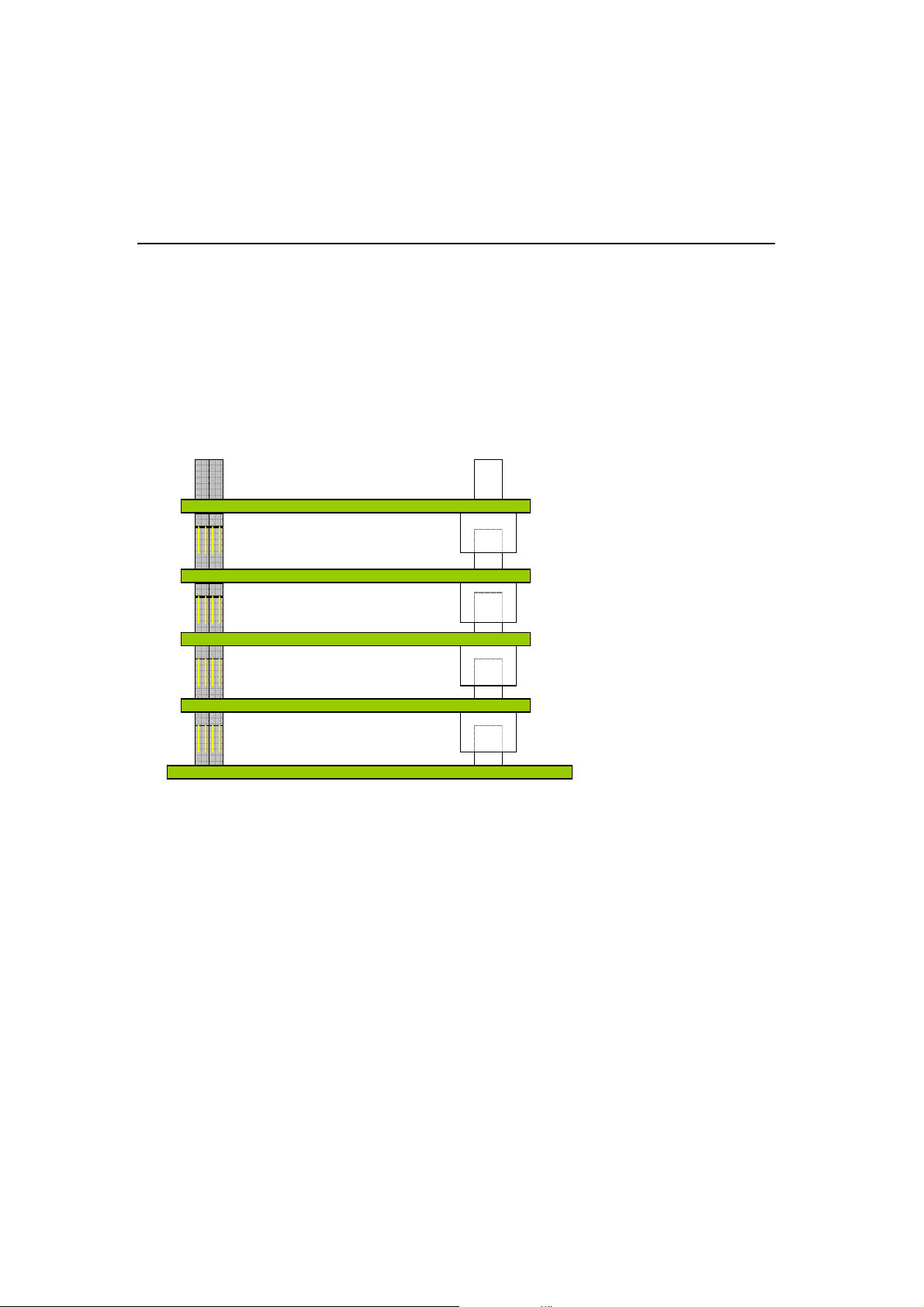
PC/104-plus is a special bus architecture designed for embedded systems. A third connector
opposite the PC/104 connectors supports the PCI bus. Basically the electrical specifications of the
PC/104-plus bus are compliant with the PCI signals, except 64-bit extensions, JTAG, PRSNT or
CLKRUN signals. The mechanical specifications are changed to “module stack”; please refer to the
figure shown below. According to the specifications of PC/104-plus, PC/104-plus modules are
installed and configured by switching CLK, IDSEL, INT, REQ and GNT signals through multiplexers
to the appropriate connections.
PC/104+ Module Slot 4
PC/104+ Module Slot 3
.
PC/104+ Module Slot 2
PC/104+ Module Slot 1
Figure 1: PC/104-plus module stack
Rotary switch on PCM-9112+ is used for these signals switching, please refer to section 2.4 for
details in this appendix.
1.2 Specifications for PCM-9112+
The specifications of the PCM-9112+ are the same as that of the PCI-9112 except for the Digital
Input and Digital Output functions have been removed from the PCM-9112+. To compensate for
the removal of the DI/DO functions, the AD FIFO has been enlarged to 512 words allowing it to
handle a wider range of applications. Please refer to section 1.3 of the PCI-9112 manual for further
details.
1.3 Supported Software
PC/104+ Host
The supported software is the same as that of the PCI-9112 without the DI/DO functions. Please
refer to section 1.4 of the PCI-9112 manual for further details.
1
Page 2
2 Installation procedures for PC/104-plus DAQ modules:
r
r
V
2.1 what you have
In addition to this appendix, the package includes the following items:
PCM-9112+ DAQ modules
Manual & Software Utility CD-ROM
If any of these items is missing or damaged, contact the dealer from whom you purchased the
product. Save the shipping materials and carton in case you want to ship or store the product in the
future.
2.2 unpacking
The card contains electro-static sensitive components that can be easily be damaged by static
electricity.
Therefore, the card should be handled on a grounded anti-static mat. The operator should be
wearing an anti-static wristband, grounded at the same point as the anti-static mat.
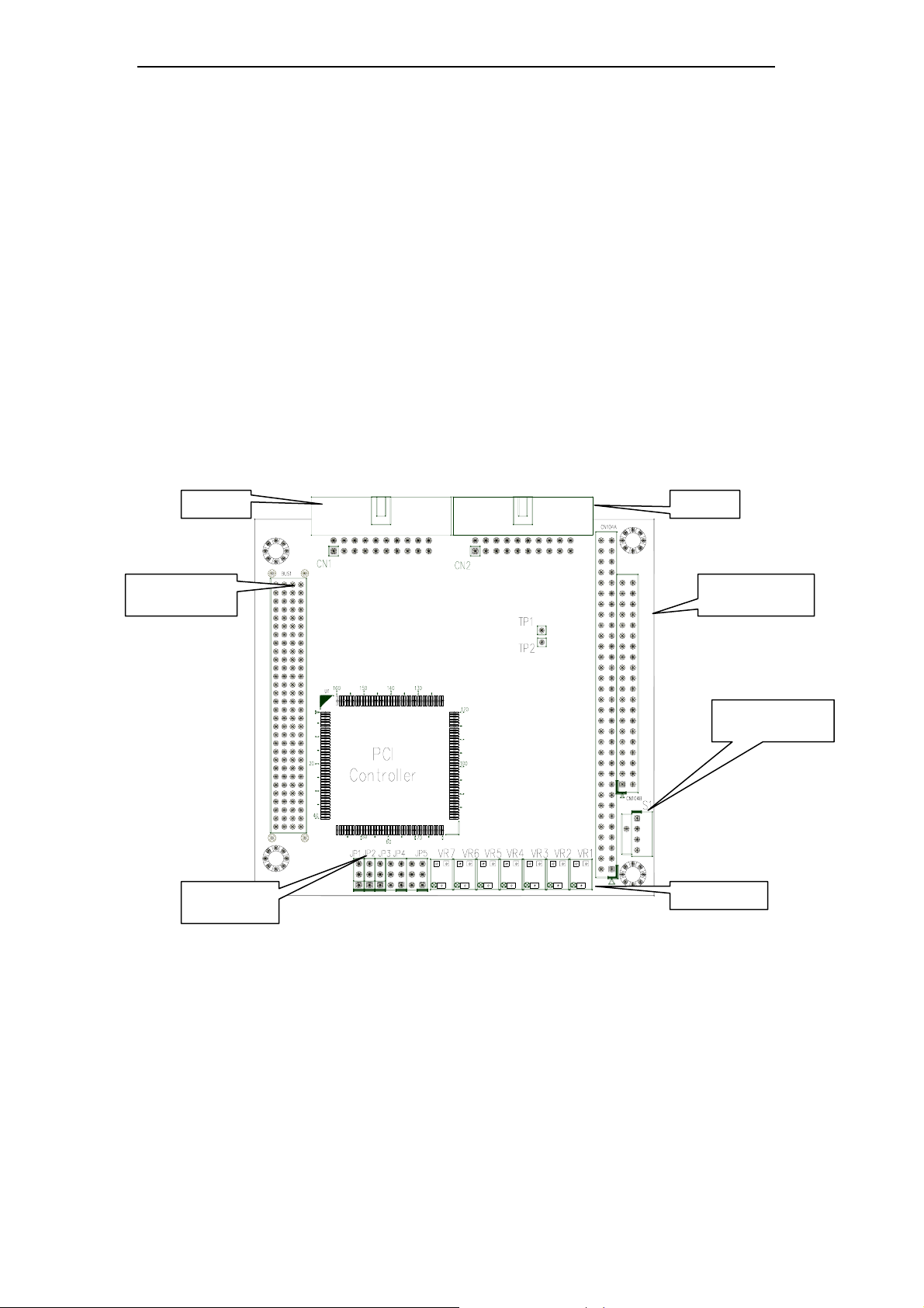
2.3 layout of modules
CN1 CN2
PC/104-plus
connecto
Jumper
JP1~JP5
PC/104
Figure 2: PCM-9112+ DAQ module layout
connecto
Rotary
switch
R1~VR7
2
Page 3
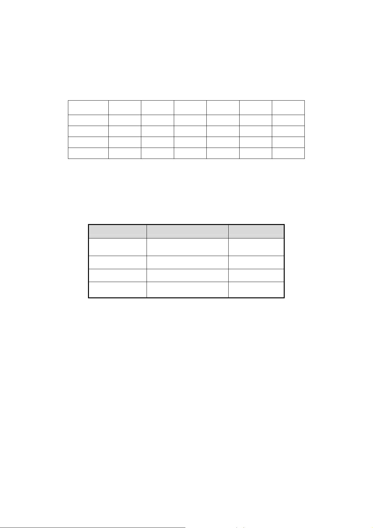
2.4 PC/104-plus configuration
A rotary switch on the PCM-9112+ is used for switching the appropriate CLK, IDSEL, INT, REQ
and GNT signals from the PCI bus. If the PCM-9112+ card is inserted in a position nearest to the
PC/104-plus motherboard, the switch must be set to 0 or 4. For signal stability, the rotary switch
should be set to the appropriate position with respect to the module slot. The module stack order
was shown in Figure 1. According to PC/104-plus specification, module slots 3 and 4 share
REQ2/GNT2, hence they cannot both have bus-mastering devices. In another word, module 3 and
4 cannot be stacked with 2 PCM-9112+ modules.
Rotary Switch
Position
0 or 4 1 CLK0 IDSEL0 INTA REQ0* GNT0*
1 or 5 2 CLK1 IDSEL1 INTB REQ1* GNT1*
2 or 6 3 CLK2 IDSEL2 INTC REQ2* GNT2*
3 or 7 4 CLK3 IDSEL3 INTD REQ2* GNT2*
* Only for Bus Master card
Module
Slot
CLK IDSEL INT REQ GNT
Table 1: Rotary switch setting
2.5 Jumpers Setting
On the PCM-9112+ DAQ module, there are 5 jumpers that need to be adjusted depending on
application requirements. The following table describes the attributes of these jumpers.
Configuration Attributes Jumpers
Analog Inputs
Clock Source
D/A Reference
Voltage
D/A Reference Source
Single-ended or
Differential Analog Input
Internal Clock or
External Clock
-10V or -5V JP3
Internal Reference or
External Reference
JP1 and JP4
JP2
JP5
Table 2: Jumpers setting
3
Page 4

2.5.1 Analog input mode configuration
The analog input channels on the PCM-9112+ DAQ module can be configured as 16 single-ended
or 8 differential inputs. Jumpers JP1 and JP4 control the analog input configuration. The setting of
JP1 and JP4 are specified below:
Single-ended
input (Default)
Differential input
Table 3: Analog input mode configurations
2.5.2 Clock Source Setting
The programmable 8254-interval timer is used in the PCM-9112+. It provides 3 independent 16-bit
programmable down counters. Input of counter 2 is connected to an accurate 2MHz oscillator used
as the internal pacer. Input of counter 1 is cascaded from the output of counter 2. Channel 0 is
free for user applications. There are two selections for the clock source of channel 0: the internal
2MHz clock or an external clock signal. The setting for clock signal is shown in the following table.
Analog Input Setting
Internal Clock
Source: 2MHz
(default)
External Clock
Source
Clock source setting
Table 4: Clock source setting
4
Page 5

2.5.3 D/A Reference Voltage External/Internal Setting
The D/A converter’s reference voltage source can be supplied either by internal or external sources.
For external reference voltage, pin 3 (ExtRef1) and 4 (ExtRef2) of connector CN2 are used.
Reference voltage source for D/A of channel 1 and 2 are selected by JP4. Possible settings are
shown below:
D/A Reference Voltage Setting
D/A CH1 is external
D/A CH2 is external
D/A CH1 is external
D/A CH2 is internal
D/A CH1 is internal
D/A CH2 is external
D/A CH1 is internal
D/A CH2 is internal
Table 5: D/A reference voltage setting
5
Page 6

2.5.4 Internal Reference Voltage Setting
The internal reference voltage can be set to either –5V or –10V by JP3. Possible configurations are
illustrated in the table below. Note that the internal reference voltage is used only when JP5 is set
to internal reference only. If –10V internal reference voltage is selected, the D/A output range is
0V~10V. On the other hand, if the –5V is selected, the D/A output range is 0V~5V.
Internal Reference Voltage Setting
-5V internal
reference
voltage
-10V internal
reference
voltage
Table 6: Internal reference voltage setting
6
Page 7

2.6 Connector Pin Assignment
g
N
N/CN
The PCM-9112+ DAQ module has two 20-pin connectors. CN1 is for analog input and CN2 for
analog output, timer/counter’s signals.
AI0
AI1
AI2
AI3
AI4
AI5
AI6
AI7
A.GND
A.GND
Figure 3: CN1 pin assignment for
1
3
5
7
9
11
13
15
17
19 20
single-ended connection
2
4
6
8
10
12
14
16
18
ExtRef2
COUT0
AI8
AI9
AI10
AI11
AI12
AI13
AI14
AI15
A.GND
A.GND
AIH0
AIH1
AIH2
AIH3
AIH4
AIH5
AIH6
AIH7
A.GND
A.GND
Figure 4: CN1 pin assignment for
V.REF AO1
10
12
14
16
18
2
4
6
8
ExtRef1
AO2
GATE0
GATE
COUT1
ExTCLK
+12V
A.GND
D.GND
ExtTr
N/C
+5V
N/C
1
3
5
7
9
11
13
15
17
19 20
1
3
5
7
9
10
11
12
13
14
15
16
17
18
19 20
differential connection
/C
/C
2
4
6
8
AIL0
AIL1
AIL2
AIL3
AIL4
AIL5
AIL6
AIL7
A.GND
A.GND
Legend:
AIn
AIHn
AILn
ExtRef n
AOn
ExtCLK
ExtTrig
GATE
COUT n
V.REF
A.GND
D.GND
Figure 5: CN2 pin assignment
: Analog input channel n (single-ended)
: Analog high input channel n (differential)
: Analog low input channel n (differential)
: External reference voltage for D/A channel n
: Analog output channel n
: External clock input
: External trigger signal
: Gate input for 8254
: Signal output of counter n
: Voltage reference
: Analog ground
: Digital ground
7
Page 8

2.7 Daughter Boards and Accessories
The PCM-9112+ DAQ module has several available accessories allowing for easy signal wiring for
measurements and control. Functionality and connections of the available accessories are describe
in the in the following sections.
2.7.1 Connect with ACLD-9137
Equipped with a 37-pin D-sub connector, the ACLD-9137 provides a simple way for connection.
Intuitively layout and reliable screw clamp terminal allows for easy wiring. In conjunction with the
ACL-10337 (two 20-pin headers to DB-37 cable), users can set up the connection immediately.
Figure 6: Connect with ACLD-9137
2.7.2 Connect with DIN-37D
The DIN-37D is a termination board with a DIN socket. When users need to mount the termination
board onto the DIN rail, it provides a convenient interface for installation. To achieve this
connection, use the following cables ACL-10337 and ACL-10137.
Figure 7: Connect with DIN-37D
8
Page 9

2.7.3 Connect with ACLD-8125
The ACLD-8125 has a 37-pin D-sub connector, which can connect to the PCM-9112+ through a
ACL-10337 and ACL-10137 cable. The most outstanding feature of this daughter board is the CJC
(cold junction compensation) circuit. You can directly connect a thermocouple onto the ACLD-8125
board. The CJC is only suitable for high gain analog input mode.
Figure 8: Connect with ACLD-8125
2.7.4 Connect with DIN-20P
The DIN-20P has a 20-pin ribbon connector with a DIN socket. This board is connected to the
PCM-9112+ via a 20-pin ribbon cable.
Figure 9: Connect with two DIN-20P termination boards
9
Page 10

Warranty Policy
Thank you for choosing ADLINK. To understand your rights and enjoy all the after-sales services we
offer, please read the following carefully.
1. Before using ADLINK’s products please read the user manual and follow the instructions exactly.
When sending in damaged products for repair, please attach an RMA application form which can be
downloaded from: http://rma.adlinktech.com/policy/.
2. All ADLINK products come with a limited two-year warranty, one year for products bought in China.
The warranty period starts on the day the product is shipped from ADLINK’s factory.
z
Peripherals and third-party products not manufactured by ADLINK will be covered by the
z
original manufacturers' warranty.
For products containing storage devices (hard drives, flash cards, etc.), please back up your
z
data before sending them for repair. ADLINK is not responsible for any loss of data.
Please ensure the use of properly licensed software with our systems. ADLINK does not
z
condone the use of pirated software and will not service systems using such software.
ADLINK will not be held legally responsible for products shipped with unlicensed software
installed by the user.
For general repairs, please do not include peripheral accessories. If peripherals need to be
z
included, be certain to specify which items you sent on the RMA Request & Confirmation
Form. ADLINK is not responsible for items not listed on the RMA Request & Confirmation
Form.
3. Our repair service is not covered by ADLINK's guarantee in the following situations:
Damage caused by not following instructions in the User's Manual.
z
Damage caused by carelessness on the user's part during product transportation.
z
Damage caused by fire, earthquakes, floods, lightening, pollution, other acts of God, and/or
z
incorrect usage of voltage transformers.
Damage caused by inappropriate storage environments such as with high temperatures,
z
high humidity, or volatile chemicals.
Damage caused by leakage of battery fluid during or after change of batteries by
z
customer/user.
Damage from improper repair by unauthorized ADLINK technicians.
z
Products with altered and/or damaged serial numbers are not entitled to our service.
z
This warranty is not transferable or extendible.
z
Other categories not protected under our warranty.
z
4. Customers are responsible for all fees necessary to transport damaged products to ADLINK.
For further questions, please e-mail our FAE staff: service@adlinktech.com
10
 Loading...