

Page 1
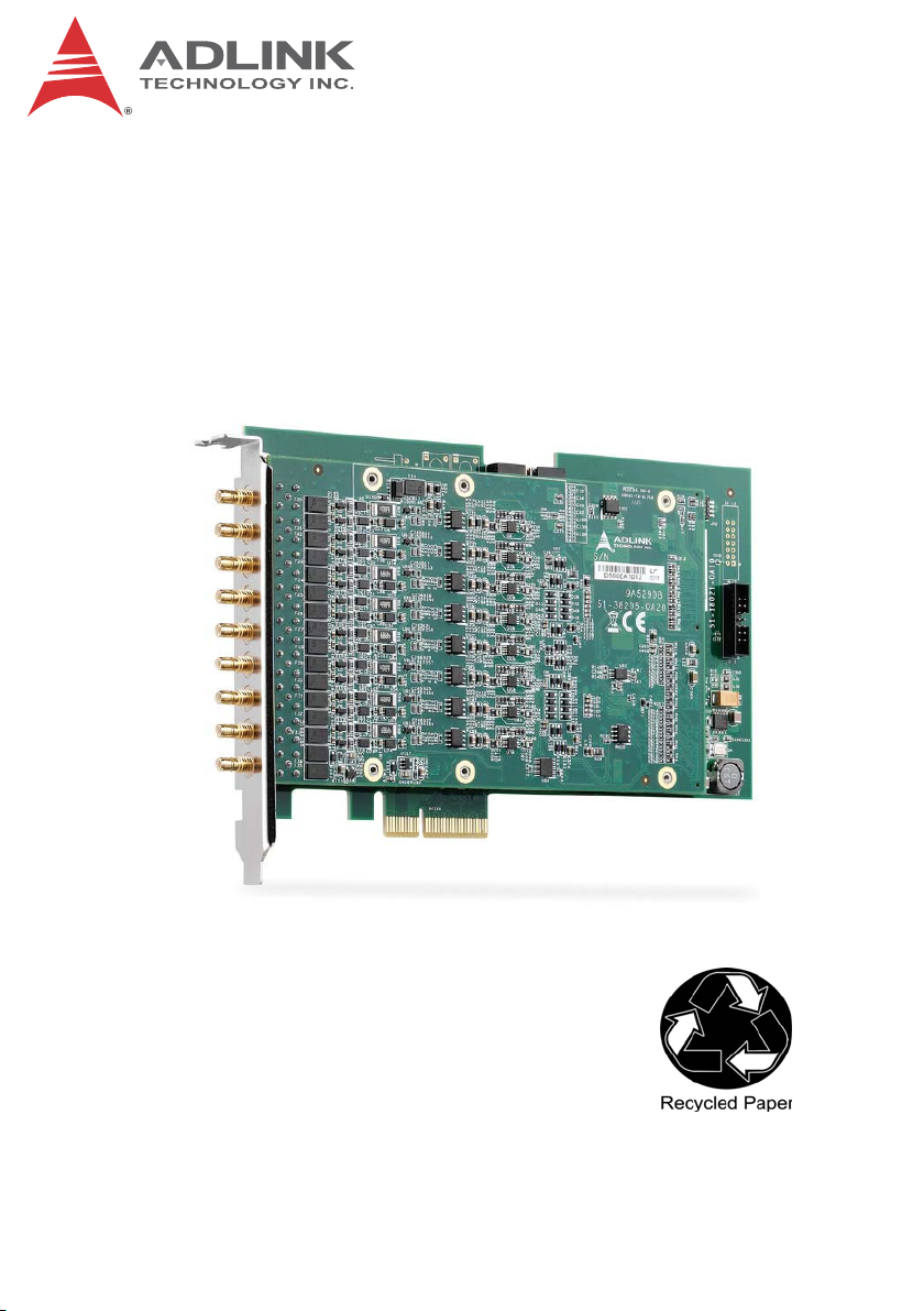
PCIe-9529
8-CH 24-Bit 192 kS/s
Dynamic Signal Acquisition Module
User’s Manual
Manual Rev.: 2.00
Revision Date: July 11, 2014
Part Number: 50-11255-1000
Advance Technologies; Automate the World.
Page 2
Revision History
Revision Release Date Description of Change(s)
2.00 July 11, 2014 Initial Release
ii
Page 3

PCIe-9529
Preface
Copyright 2014 ADLINK Technology, Inc.
This document contains proprietary information protected by copyright. All rights are reserved. No part of this manual may be reproduced by any mechanical, electronic, or other means in any form
without prior written permission of the manufacturer.
Disclaimer
The information in this document is subject to change without prior
notice in order to improve reliability, design, and function and does
not represent a commitment on the part of the manufacturer.
In no event will the manufacturer be liable for direct, indirect,
special, incidental, or consequential damages arising out of the
use or inability to use the product or documentation, even if
advised of the possibility of such damages.
Environmental Responsibility
ADLINK is committed to fulfill its social responsibility to global
environmental preservation through compliance with the European Union's Restriction of Hazardous Substances (RoHS) directive and Waste Electrical and Electronic Equipment (WEEE)
directive. Environmental protection is a top priority for ADLINK.
We have enforced measures to ensure that our products, manufacturing processes, components, and raw materials have as little
impact on the environment as possible. When products are at their
end of life, our customers are encouraged to dispose of them in
accordance with the product disposal and/or recovery programs
prescribed by their nation or company.
Conventions
Take note of the following conventions used throughout this
manual to make sure that users perform certain tasks and
instructions properly.
Preface iii
Page 4
NOTE:
NOTE:
CAUTION:
WARNING:
Additional information, aids, and tips that help users perform
tasks.
Information to prevent minor physical injury, component damage, data loss, and/or program corruption when trying to complete a task.
Information to prevent serious physical injury, component
damage, data loss, and/or program corruption when trying to
complete a specific task.
iv Preface
Page 5

PCIe-9529
Table of Contents
Preface .................................................................................... iii
List of Figures ....................................................................... vii
List of Tables.......................................................................... ix
1 Introduction ........................................................................ 1
1.1 Features............................................................................... 1
1.2 Applications ......................................................................... 1
1.3 Specifications....................................................................... 2
1.3.1 Analog Input ............................................................... 2
1.3.2 Timebase....................................................................9
1.3.3 Triggers ...................................................................... 9
1.3.4 General Specifications................................................ 9
1.4 Schematics and I/O ........................................................... 11
1.5 Software Support ............................................................... 13
1.5.1 SDK .......................................................................... 13
1.5.2 DSA-DASK ............................................................... 13
2 Getting Started ................................................................. 15
2.1 Package Contents ............................................................. 15
2.2 Installation Environment .................................................... 15
2.3 Installing the Module.......................................................... 16
3 Operations ........................................................................ 17
3.1 Functional Block Diagram.................................................. 17
3.2 Analog Input Channel ........................................................ 17
3.2.1 Analog Input Front-End Configuration ...................... 17
3.2.2 Input Range and Data Format .................................. 19
3.2.3 ADC and Analog Input Filter.....................................19
3.2.4 DMA Data Transfer................................................... 20
Table of Contents v
Page 6

3.3 Trigger Source and Trigger Modes .................................... 22
3.4 Trigger Mode...................................................................... 25
3.5 ADC Timing Control ........................................................... 27
3.5.1 Timebase..................................................................27
3.5.2 DDS Timing vs. ADC ................................................ 27
3.5.3 Filter Delay in ADC ................................................... 27
3.6 Synchronizing Multiple Modules ........................................ 28
3.6.1 SSI_TIMEBASE........................................................ 29
3.6.2 SSI_SYNC_START .................................................. 29
3.6.3 SSI_AD_TRIG ..........................................................30
A Appendix: Calibration....................................................... 31
A.1 Calibration Constant .......................................................... 31
A.2 Auto-Calibration ................................................................. 31
Important Safety Instructions.............................................. 33
Getting Service ..................................................................... 35
vi Table of Contents
Page 7

PCIe-9529
List of Figures
Figure 1-1: Analog Input Channel Bandwidth, -1dBFS 108kS/s ... 6
Figure 1-2: Analog Input Channel Bandwidth, -1dBFS 108kS/s ... 7
Figure 1-3: Spurious Free Dynamic Range 54kS/s ...................... 7
Figure 1-4: Spurious Free Dynamic Range 108kS/s .................... 8
Figure 1-5: Spurious Free Dynamic Range 192kS/s .................... 8
Figure 1-6: PCIe-9529 Side View ............................................... 11
Figure 1-7: PCIe-9529 I/O Array ................................................. 12
Figure 3-1: Analog Input Architecture ......................................... 17
Figure 3-2: Linked List of PCI Address DMA Descriptors ........... 21
Figure 3-3: Trigger Architecture .................................................. 22
Figure 3-4: External Digital Trigger ............................................. 23
Figure 3-5: Analog Trigger Conditions ........................................ 24
Figure 3-6: Post-Trigger Acquisition ........................................... 25
Figure 3-7: Delay Trigger Mode Acquisition................................ 26
Figure 3-8: Re-Trigger Mode Acquisition .................................... 26
Figure 3-9: Timebase Architecture.............................................. 27
Figure 3-10: SSI Architecture........................................................ 29
List of Figures vii
Page 8

This page intentionally left blank.
viii List of Figures
Page 9

PCIe-9529
List of Tables
Table 1-1: Timebase......................................................................... 9
Table 1-2: Trigger Source & Mode.................................................... 9
Table 1-3: Digital Trigger Input .........................................................9
Table 3-1: Input Range and Data Format ....................................... 19
Table 3-2: Input Range Midscale Values........................................ 19
Table 3-3: ADC Sample Rates vs DDS Output Clock..................... 20
Table 3-4: Preferred Characteristics for Analog Triggers ...............24
Table 3-5: Timing Relationship between ADC and PLL Clock........ 27
Table 3-6: ADC Filter Delay ............................................................ 28
Table 3-7: SSI Timing Signal Definitions ........................................28
List of Tables ix
Page 10

This page intentionally left blank.
x List of Tables
Page 11

1 Introduction
The PCIe-9529 is a high-performance 8-CH 24-Bit 192 kS/s
dynamic signal acquisition module, specifically designed for applications such as structural health monitoring, noise, vibration, and
harshness (NVH) measurement, and phased array data acquisition.
The PCIe-9529 features 24-bit simultaneous sampling at 192 kS/s
over 8 channels, and a 110 dB dynamic range, providing ample
power for high-density, high channel count signal measurement,
and vibration-optimized lower AC cutoff frequency of 0.5 Hz. All
input channels incorporate 4 mA bias current for integrated electronic piezoelectric (IEPE) signal conditioning for accelerometers
and microphones.
The PCIe-9529 is auto-calibrated with an onboard reference circuit calibrating offset and acquiring analog input errors. Following
auto-calibration, the calibration constant is stored in EEPROM,
such that these values can be loaded and used as needed by the
board. There is no requirement to calibrate the module manually.
1.1 Features
X PCI Express specification Rev. 1.1 compliant
X 8 simultaneous analog inputs
X 192 kS/s maximum sampling rate
X AC or DC input coupling, software selectable
X Support for:
Z One external digital trigger input
Z IEPE output on each analog input, software configurable
Z Auto-calibration
PCIe-9529
1.2 Applications
X Structural health monitoring
X Phase array data acquisition
X Noise, vibration, and harshness (NVH) detection
X Machine status monitoring
Introduction 1
Page 12
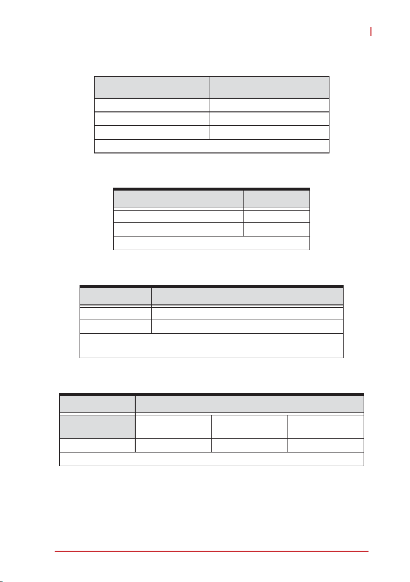
1.3 Specifications
1.3.1 Analog Input
Channel Characteristics
Channels 8
Type Differential or pseudo-differential
Coupling AC or DC, software selectable
AC coupling cutoff
frequency
ADC resolution 24-Bit
ADC type Delta-sigma
Input signal range ±10V, ±1V
Sampling rate (FS)
Over voltage
protection
Input impedance
Offset error ±1 mV max.
Gain error ±0.1% of FSR
IEPE Current
IEPE Compliance 24V
0.5Hz
8 kS/s to 192 kS/s,
768 S/s increments for Fs > 108 kS/s,
576 S/s increments for 54 kS/s Fs 108 kS/s
192 S/s increments for 8KS/s Fs 54kS/s
Differential:
±42.4V,
Pseudo-differential:
>>positive terminal ±42.4 V
>>negative terminal unprotected, rated at ±2.5 V
1M, (50 between negative input and system
ground for pseudo-differential mode)
4 mA, each channel independently software
configurable
2 Introduction
Page 13
System Noise
PCIe-9529
Sample Rate (kS/s)
Fs = 54 kS/s 37.4
Fs = 108 kS/s 66.5
Fs = 192 kS/s 74.6
1. Shorted input
System Noise1 (LSB
Common Mode Rejection Ratio (CMRR)
Input Range (V)
±1V 65
±10V 80
1. Input frequency < 1 kHz
CMRR1 (dB)
-3 dB Bandwidth
1
Sample rate
Fs < 108 kS/s >0.4863 FS
Fs > 108 kS/s >0.22 FS
1. Disable digital filter when Fs < 108 kS/s; Enable digital filter
when Fs > 108 kS/s
-3 dB bandwidth
rms
1
)
Flatness
Flatness (dB)
Input Range (V)
±1V, ±10V 0.06 0.08 0.1
1. Relative to 1 kHz
Introduction 3
54 kS/s
20 Hz to 22 kHz
108 kS/s
20 Hz to 45 kHz
1
192 kS/s
20 Hz to 42 kHz
Page 14
Spurious Free Dynamic Range (SFDR)
SFDR (dBc)
Input Range (V) Fs = 54 kS/s Fs = 108 kS/s Fs = 192 kS/s
±1V, ±10V 104 104 105
1. 1 kHz input tone and -1 dBFS input amplitude.
2. Measurement Includes harmonics.
1,2
Dynamic Range
Dynamic Range (dBFS)
Input Range (V) Fs = 54 kS/s Fs = 108 kS/s Fs = 192 kS/s
±1V, ±10V 107 100 100
1. 1 kHz input tone and -60 dBFS input amplitude
1
System to Noise Ratio
SNR (dBc)
Input Range (V) Fs = 54 kS/s Fs = 108 kS/s Fs = 192 kS/s
±1V, ±10V 104 99 98
1. 1 kHz input tone and -1 dBFS input amplitude
1
Total Harmonic Distortion (THD)
THD (dBc)
Input Range (V) Fs = 54 kS/s Fs = 108 kS/s Fs = 192 kS/s
±1V -106 -106 -107
±10V -104 -104 -105
1. 1 kHz input tone and -1 dBFS input amplitude
4 Introduction
1
Page 15

Total Harmonic Distortion plus noise (THD+N)
PCIe-9529
THD+N (dBc)
Input Range (V)
±1V -96 -94 -95
±10V -96 -92 -95
1. 1 kHz input tone and -1 dBFS input amplitude
54 kS/s
20 Hz to 22 kHz
108 kS/s
20 Hz to 45 kHz
1
192 kS/s
20 Hz to 42 kHz
Intermodulation Distortion
IMD (dBc)
Input Range (V) Fs = 54 kS/s Fs = 108 kS/s Fs = 192 kS/s
±1V -103 -99 -99
±10V -105 -101 -101
1. CCIF 14 kHz + 15 kHz
2. -6 dBFS input amplitude for each tone
1,2
Crosstalk
Crosstalk (dBc)
Input Range (V) 1 kHz 0.5 Fs
±1V, ±10V -100 -97
1. Shorted input
2. -1 dBFS input amplitude
1,2
Interchannel Gain Mismatch
Input Range (V)
±1V, ±10V 0.1
1. 1 kHz input tone and -1 dBFS input amplitude
Introduction 5
Gain Mismatch (dB)
1
Page 16

Interchannel Phase Mismatch
Input Range (V)
±1V, ±10V
Phase Mismatch (°)
1 khz 20 khz 86.4 khz
0.1 0.442 1.64
1
1. -1 dBFS input amplitude
0
−5
−10
−15
Magnitude (dB)
−20
−25
2
10
Magnitude Response
3
10
Frequency (Hz)
4
10
5
10
Figure 1-1: Analog Input Channel Bandwidth, -1dBFS 108kS/s
6 Introduction
Page 17

PCIe-9529
0
−0.5
−1
−1.5
−2
−2.5
Magnitude (dB)
−3
−3.5
−4
−4.5
−1
10
Response when AC coupling enabled
0
10
Frequency (Hz)
1
10
Figure 1-2: Analog Input Channel Bandwidth, -1dBFS 108kS/s
0
−20
SFDR 54 kS/s (1V Input Range, −1 dBFS and 1 kHz Sine Wave Input)
−40
−60
−80
Magnitude (dB)
−100
−120
−140
−160
0 0.5 1 1.5 2 2.5
Frequency (Hz)
x 10
4
Figure 1-3: Spurious Free Dynamic Range 54kS/s
Introduction 7
Page 18

0
−20
−40
−60
−80
Magnitude (dB)
−100
−120
−140
−160
0 0.5 1 1.5 2 2.5 3 3.5 4 4.5 5
SFDR 108 kS/s (1V Input Range, −1 dBFS and 1 kHz Sine Wave Input)
Frequency (Hz)
Figure 1-4: Spurious Free Dynamic Range 108kS/s
x 10
4
0
−20
−40
−60
−80
Magnitude (dB)
−100
−120
−140
−160
0 1 2 3 4 5 6 7 8 9
SFDR 192 kS/s (1V Input Range, −1 dBFS and 1 kHz Sine Wave Input)
Frequency (Hz)
x 10
4
Figure 1-5: Spurious Free Dynamic Range 192kS/s
8 Introduction
Page 19

PCIe-9529
1.3.2 Timebase
Sampling Clock
Sampling Clock
Timebase
Delay Trigger Timebase PCIe clock (125 MHz)
Internal: onboard synthesizer (10 MHz, accuracy
< ± 25ppm)
External: SSI
Table 1-1: Timebase
1.3.3 Triggers
Trigger Source & Mode
Trigger source Software, external digital trigger, analog trigger, and SSI
Trigger mode Post trigger and delay trigger
Table 1-2: Trigger Source & Mode
Digital Trigger Input
Sources Front panel SMB connector
Compatibility 3.3 V TTL, 5 V tolerant
Input high threshold 2.0 V
Input low threshold (VIL) 0.8 V
Maximum input overload -0.5 V to +5.5 V
Trigger polarity Rising or falling edge
Pulse width 20 ns minimum
Table 1-3: Digital Trigger Input
1.3.4 General Specifications
Physical
Physical dimensions 167.64W x 106.68H mm (6.53 x 4.16 in)
Bus
Bus interface PCI Express x 4
Environmental Tolerance
Introduction 9
Page 20

Operating
Storage
Calibration
Onboard reference +5.000 V
Temperature coefficient < 5.0 ppm/°C
Warm-up time 15 minutes
Power Consumption
Power Rail Standby Current (mA) Full Load (mA)
+3.3 V 584 630
+12 V 904 1160
Temperature: 0°C - 55°C
Relative humidity: 10% - 90%, non-condensing
Temperature: -20°C - +80°C
Relative humidity: 10% - 90%, non-condensing
10 Introduction
Page 21

1.4 Schematics and I/O
All dimensions are in mm
NOTE:
NOTE:
100.36
PCIe-9529
59.05
176.42
Figure 1-6: PCIe-9529 Side View
Introduction 11
Page 22

The PCIe-9529 I/O array is labeled to indicate connectivity, as
shown.
Figure 1-7: PCIe-9529 I/O Array
12 Introduction
Page 23

PCIe-9529
1.5 Software Support
ADLINK provides versatile software drivers and packages to suit
various user approaches to building a system. Aside from programming libraries, such as DLLs, for most Windows-based systems, ADLINK also provides drivers for other application
environments such as LabVIEW®.
1.5.1 SDK
For customers who want to write their own programs, ADLINK provides the following software development kits.
Z DAQPilot for LabVIEW
Z Toolbox adapter for MATLAB
1.5.2 DSA-DASK
DSA-DASK includes device drivers and DLL for Windows XP/7/8.
DLL is binary compatible across Windows XP/7/8. This
means all applications developed with DSA-DASK are compatible with these Windows operating systems. The development
environment may be VB, VB.NET, VC++, BCB, and Delphi, or
any Windows programming language that allows calls to a DLL.
The DSA-DASK user and function reference manuals are on the
ADLINK All-in-One CD.
Introduction 13
Page 24

This page intentionally left blank.
14 Introduction
Page 25

2 Getting Started
This chapter describes proper installation environment, installation
procedures, package contents and basic information users should
be aware of regarding the PCIe-9529.
Diagrams and illustrated equipment are for reference only.
Actual system configuration and specifications may vary.
NOTE:
NOTE:
2.1 Package Contents
X PCIe-9529 dynamic signal acquisition module
X ADLINK All-in-One compact disc
X PCIe-9529 Quick Start Guide
If any of these items are missing or damaged, contact the dealer
2.2 Installation Environment
When unpacking and preparing to install, please refer to Important
Safety Instructions.
Only install equipment in well-lit areas on flat, sturdy surfaces with
access to basic tools such as flat- and cross-head screwdrivers,
preferably with magnetic heads as screws and standoffs are small
and easily misplaced.
Recommended Installation Tools
X Phillips (X-head) screwdriver
X Flat-head screwdriver
X Anti-static wrist strap
X Antistatic mat
ADLINK PCIe-9529 DSA modules are electrostatically sensitive
and can be easily damaged by static electricity. The module must
be handled on a grounded anti-static mat. The operator must wear
an anti-static wristband, grounded at the same point as the
anti-static mat.
PCIe-9529
Getting Started 15
Page 26

Inspect the carton and packaging for damage. Shipping and handling could cause damage to the equipment inside. Make sure that
the equipment and its associated components have no damage
before installation.
The equipment must be protected from static discharge and
physical shock. Never remove any of the socketed parts
CAUTION:
WARNING:
except at a static-free workstation. Use the anti-static bag
shipped with the product to handle the equipment and wear a
grounded wrist strap when servicing.
Do not install or apply power to equipment that is damaged or
missing components. Retain the shipping carton and packing
materials for inspection. Please contact your ADLINK
dealer/vendor immediately for assistance and obtain authorization before returning any product.
2.3 Installing the Module
1. Turn off the computer.
2. Remove the top cover.
3. Select an available PCI express x4 slot and remove the
bracket-retaining screw and the bracket cover.
4. Line up the PCI express digitizer with the PCI express
slot on the back panel. Slowly push down on the top of
the PCI express digitizer until its card-edge connector is
resting on the slot receptacle.
5. Install the bracket-retaining screw to secure the PCI
express digitizer to the back panel rail.
6. Replace the computer cover.
16 Getting Started
Page 27

3 Operations
This chapter contains information regarding analog input, trigger-
ing and timing for the PCIe-9529.
3.1 Functional Block Diagram
JFET
CH0
CH1
CH2
CH3
CH4
CH5
CH6
CH7
TRG IN
Buffer
OPAMP
BUF
BUF
BUF
BUF
Reference &
Calibration
BUF
BUF
BUF
BUF
IO
Control
PGA
PGA
PGA
PGA
PGA
PGA
PGA
PGA
PGA
PGA
Quad
24bit ADC
ADC
ADC
ADC
ADC
Quad
24bit ADC
ADC
ADC
ADC
ADC
2-bit /12.288MHz
ADC Ctrl
CLK
Synthesizer
2-bit / 12.288MHz
ADC Ctrl
DC-DC\
LDO
SSI_TIMEBASE
10 MHz
ADC
BUS
Digital
BUS
Board to Board Conn x2
3.3V
5V
12V
PCIe Controller
FPGA
ADC Control
Trigger Control
Data Processing
FIFO Interface
3.3V
5V
12V
PCIe-9529
SSI Bus [0..7]
SSI
PCIe Gen1
x4
Connector
PCIe Gen1 x4 Slot
3.2 Analog Input Channel
3.2.1 Analog Input Front-End Configuration
Signal Switch
CAL+
IEPE+
330nF / 25V
SPST
49.9R
SPST
SPST
330nF / 25V
CAL-
IEPE-
Vref
10k
10k
1MR
1MR
Cal+
Figure 3-1: Analog Input Architecture
Operations 17
JFET OPAMP
JFET OPAMP
X1
X10
PGA
24-bit ADC
10k
10k
DATA
SCK
ADC Ctrl
CARR
Vref
Page 28

Differential and Pseudo-Differential Input Configuration
The PCIe-9529 provides both differential and psuedo-differen-
tial input configurations, with differential input mode providing
voltage to the anode and cathode inputs of the SMB connector
according to signal voltage difference therebetween. If the signal source is ground-referenced, differential input mode can be
used for common-mode noise rejection.
If the signal source is a floating signal, pseudo-differential input
mode can provide a reference ground connected to the cathode input of the SMB through a 50 resistor, preventing the
floating source from drifting over the input common-mode
range.
Recommended configurations for the signal sources are as follows.
Signal Source Type Card Configuration
Floating Pseudo Differential
Ground-Reference Differential
AC and DC Input Coupling
AC and DC coupling are available. With DC coupling, DC offset
present in the input signal is passed to ADC, and is indicated if
the signal source has a small level of offset voltage or if DC
content of the signal is important. In AC coupling, the DC offset
present in the input signal is erased, and is indicated if the DC
content of the input signals is to be rejected. AC coupling
enables a high pass R-C filter through the input signal path.
The corner frequency (-3dB) is about 0.5Hz.
Input for IEPE
For applications that require sensors such as accelerometers
or microphones, the PCIe-9529 provides an excitation current
source. The common excitation current is usually about 4mA
for these IEPE sensors. A DC voltage offset is generated due
to the excitation current and sensor impedance. When IEPE
current sources are enabled, the PCIe-9529 automatically sets
input configuration to AC coupling.
18 Operations
Page 29

PCIe-9529
3.2.2 Input Range and Data Format
When using an A/D converter, properties of the signal to be measured should be considered prior to selecting channel and signal
connection to the module. A/D acquisition is initiated by a trigger
source, which must be predetermined. Data acquisition commences once the trigger condition is established. Following completion of A/D conversion, A/D data is buffered in a Data FIFO,
and can then be transferred to PC memory for further processing.
Transfer characteristics of the two input ranges of the PCIe-9529
are as follows. Data format of the PCIe-9529 is 2’s complement.
.
Description
Bipolar Analog
Input
Digital Code N/A N/A 7FFFFF 800000
Description Midscale +1LSB Midscale Midscale –1LSB
Bipolar Analog
Input
Digital Code 000001 000000 -FFFFFF
Full-scale
range
±10 V 1.19 V 9.99999881 V -10 V
±1V 0.119 V 0.999999881V -1 V
Table 3-1: Input Range and Data Format
1.19 V 0 V -1.19 V
0.119 V 0 V -0.119 V
Table 3-2: Input Range Midscale Values
Least
significant
bit
FSR-1LSB -FSR
3.2.3 ADC and Analog Input Filter
ADC (Analog-to-Digital Converter)
The PCIe-9529 provides sigma-delta analog-to-digital converters,
suitable for vibration, audio, and acoustic measurement. Analog
side of the sigma-delta ADC is 1-bit, and the digital side performs
oversampling, noise shaping and digital filtering. For example, if a
desired sampling rate is 108kS/s, each ADC samples input signals
Operations 19
Page 30

at 27.648MS/s, 256 times the sampling rate. The 1-bit 27.648MS/s
data streams from 1-bit ADC to its internal digital filter circuit to
produce 24-bit data at 108kS/s. The noise shaping removes quantization noise from low frequency to high frequency. At the last
stage, the digital filter improves ADC resolution and removes high
frequency quantization noise. The relationship between ADC sample rate and DDS output clock is as follows.
Sampling Rate DDS(PLL) CLK
8k to 54kS/s 6.144M~41.472MHz
54K to 108kS/s 13.824 M to 27.648 MHz
108K to 192kS/s 20.736 M to 36.864 MHz
Table 3-3: ADC Sample Rates vs DDS Output Clock
Filter
Each channel has a two-pole lowpass filter. The filters limit bandwidth of the signal path and reject wideband noise.
3.2.4 DMA Data Transfer
The PCIe-9529, as a PCIe Gen1 X 4 device, provides a 192KS/s
sampling rate ADC, generating a 3.072 MByte/second rate. To
provide efficient data transfer, a PCI bus-mastering DMA is essential for continuous data streaming, as it helps to achieve the full
potential PCI Express bus bandwidth. The bus-mastering controller releases the burden on the host CPU since data is directly
transferred to the host memory without intervention. Once analog
input operation begins, the DMA returns control of the program.
During DMA transfer, the hardware temporarily stores acquired
data in the onboard AD Data FIFO, and then transfers the data to
a user-defined DMA buffer in the computer.
Using a high-level programming library for high speed DMA data
acquisition, the sampling period and the number of conversions
needs simply to be assigned into specified counters. After the AD
trigger condition is met, the data will be transferred to the system
memory by the bus-mastering DMA. In a multi-user or multi-task-
20 Operations
Page 31

PCIe-9529
r
r
r
ing OS, such as Microsoft Windows, Linux, or other, it is difficult to
allocate a large continuous memory block. Therefore, the bus controller provides DMA transfer with
scatter-gather function to link non-contiguous memory blocks into
a linked list to enable transfer of large amounts of data without
memory limitations. In non-scatter-gather mode, the maximum
DMA data transfer size is 2 MB double words (8 MB bytes); in
scatter-gather mode, there is no limitation on DMA data transfer
size except the physical storage capacity of the system. Users can
also link descriptor nodes circularly to achieve a multibuffered
DMA. A linked list comprising three DMA descriptors. Each
descriptor contains a PCI address, PCI dual address, a transfer
size, and the pointer to the next descriptor.PCI address and PCI
dual address support 64-bit addresses which can be mapped into
more than 4 GB of address space, as shown.
First PCI Address PCI Address PCI Address
First Dual Address Dual Address
Transfer Size
Next Descripto
Transfer Size
Next Descripto
Dual Address
Transfer Size
Next Descripto
PCI Bus
Local Memory
(FIFO)
Figure 3-2: Linked List of PCI Address DMA Descriptors
Operations 21
Page 32

3.3 Trigger Source and Trigger Modes
SMB Connector
Analog CH0
Analog CH1
Analog CH2
Analog CH3
Analog CH4
Analog CH5
Analog CH6
Analog CH7
Software Trigger
TRG IN
Digital Trigger Input
Analog
Trigger
Analog
Trigger
Selection
Trigger Source Mux
SSI_AD_TRIG
SSI BUS [5]
Trigger
Decision
To Internal
Circuit
SSI_AD_TRIG
Figure 3-3: Trigger Architecture
The PCIe-9529 requires a trigger to implement acquisition of data.
Configuration of triggers requires identification of trigger
source. The PCIe-9529 supports internal software trigger, external
digital trigger and SSI Bus Number 5 as well as analog trigger.
Software Trigger
The software trigger, generated by software command, is
asserted immediately following execution of specified function
calls to begin the operation.
SSI BUS [5]
External Digital Trigger
An external digital trigger is generated when a TTL rising edge
or a falling edge is detected at the SMB connector on the front
panel. As shown, trigger polarity can be selected by software.
Note that the signal level of the external digital trigger signal
should be TTL compatible, with minimum pulse width 10ns.
22 Operations
Page 33

PCIe-9529
Pulse Width > 20ns
Rising
edge trigger
event
SSI_AD_TRIG
The PCIe-9529 utilizes SSI Bus Number 5 to act as a System
Synchronization Interface (SSI). With the interconnected bus
provided by SSI Bus, multiple modules are easily synched.
When configured as input the PCIe-9529 serves as a slave
module and can accept trigger signals from SSI Bus Number 5,
asserted from other PCIe-9529 modules. When configured as
output, the PCIe-9529 serves as a master module and can output trigger signals to SSI Bus Number 5.
Analog Trigger
The PCIe-9529 analog trigger circuitry can be configured to
monitor one analog input channel from which data is acquired.
Selection of an analog input channel as the analog trigger
channel does not influence the input channel acquisition operation. The analog trigger circuit generates an internal digital trigger signal based on the condition between the analog signal
and the defined trigger level.
Analog trigger conditions are as follows:
Z Positive-slope trigger: The trigger event occurs when the
analog input signal changes from a voltage lower than
Figure 3-4: External Digital Trigger
Pulse Width > 20ns
Falling
edge trigger
event
Operations 23
Page 34

the specified trigger level to a voltage exceeding the
specified trigger level.
Z Negative-slope trigger: The trigger event occurs when
the analog input signal changes from a voltage exceeding the specified trigger level to a voltage lower than the
specified trigger level.
Positive-Slope Trigger Event
Occurs
Negative-Slope Trigger
Event Occurs
Trigger Level
Analog
Signal
Figure 3-5: Analog Trigger Conditions
Trigger signal can be chosen from among CH0, CH1,
CH2,CH3, CH4, CH5, CH6 and CH7 during use of an external
analog trigger source. The trigger level can be set by software
with 24-bit resolution, with characteristics as shown.
Trigger Level
Setting (Hex)
7FFFFF 9.99999881 V 0.999999881 V
7FFFFE 9.99999762 V 0.999999762 V
1 1.19 V 0.119 V
00V 0V
FFFFFF -1.19 V -0.119 V
800001 -9.99999881 V -0.999999881 V
800000 -10 V -1 V
Trigger Voltage
(-10V to +10V Range)
Trigger Voltage
(-1V to +1V Range)
Table 3-4: Preferred Characteristics for Analog Triggers
24 Operations
Page 35

PCIe-9529
Trigger Export
The PCIe-9529 utilizes SSI Bus Number 5 to act as a System
Synchronization Interface (SSI). With the interconnected bus
provided by SSI Bus, multiple modules are easily synched.
When configured as input the PCIe-9529 serves as a slave
module and can accept trigger signals from SSI Bus Number 5,
asserted from other PCIe-9529 modules. When configured as
output, the PCIe-9529 serves as a master module and can output trigger signals to SSI Bus Number 5.
3.4 Trigger Mode
Two trigger modes applied to trigger sources initiate different data
acquisition timings when a trigger event occurs, as applied to
analog input and output functions.
Post Trigger Mode
If post trigger mode is configured, activity commences once the
following trigger conditions are met:
Z The analog input channel acquires a programmed num-
ber of samples at a specified sampling rate
Z The analog output channel outputs pre-defined voltage
at a specified output rate
Figure 3-6: Post-Trigger Acquisition
Delay Trigger Mode
If delay trigger mode is configured, delay time from when the
trigger event asserts to the beginning of the acquisition and
waveform generation can be specified, as shown. Delay time is
Operations 25
Page 36

specified by a 32-bit counter value with the counter clocking
based on the PCIe clock. Accordingly, maximum delay time is
the period of PCIe_CLK X (2^32 - 1) and minimum is the period
of PCIe_CLK (8 ns).
Figure 3-7: Delay Trigger Mode Acquisition
Post-Trigger or Delay-Trigger Acquisition with Re-Trigger
Post-trigger or delay trigger acquisition with re-trigger function
enables collection of data after several trigger events, as
shown. When the number of triggers is defined, the PCIe-9529
acquires specific sample data each time a trigger is accepted.
All sampled data is stored in onboard memory first, until all trig-
ger events have occurred, such that time between the previous
sampled data and the subsequent trigger event can be only
one clock period of PCIe CLK. After the initial setup, no additional software intervention is required.
Operation
Trigger
Data
1st Trigger Event Occurs
start
2nd Trigger Event Occurs
Time
N samples N samples
Figure 3-8: Re-Trigger Mode Acquisition
26 Operations
Page 37

PCIe-9529
3.5 ADC Timing Control
3.5.1 Timebase
Onboard
Oscillator
10M
SYNC_CLK
ADC0_CLK
SSI_TIMEBASE
SSI Bus [0]
1-to-4 Clock
Timebase Clock Mux
Buffer & PLL
FPGA_MCLK
ADC1_CLK
Figure 3-9: Timebase Architecture
An onboard timebase clock drives the sigma-delta ADC, with fre-
quency exceeding the sample rate and produced by a PLL chip,
with output frequency programmable to superior resolution. The
PCIe- 9529 accepts the external timebase from SSI Bus Number 0
for synchronization between modules.
3.5.2 DDS Timing vs. ADC
SSI_TIMEBASE
SSI Bus [0]
Sampling Rate 8k – 54kS/s 54k - 108kS/s 108 k – 192kS/s
DDS(PLL) CLK
6.144
M-41.472
MHz
13.824
M-27.648 MHz
20.736
M-36.864 MHz
Table 3-5: Timing Relationship between ADC and PLL Clock
3.5.3 Filter Delay in ADC
Filter delay indicates time required for data propagation through a
converter. Both AI channels experience filter delay due to filter
circuitry and converter architecture, as shown.
Update Rate (kS/s) Filter Delay (samples)
8 K - 54 kS/s 13
54 K - 108 kS/s 13
Operations 27
Page 38

Update Rate (kS/s) Filter Delay (samples)
108 K-192 kS/s 5
Table 3-6: ADC Filter Delay
3.6 Synchronizing Multiple Modules
The SSI (System Synchronization Interface) provides DAQ timing
synchronization between multiple cards, with a bidirectional SSI
I/O providing flexible connection between cards and allowing a
single SSI master to output the signal to other slave modules. SSI
signals are designed for card synchronization only, not external
devices. All SSI signals are routed to the CN4 connector and the
eight interconnected lines on the CN4, labeled SSI Bus [0:7] provide a flexible interface for synching multiple modules with the
requirement of cabling. The PCIe-9529 utilizes the SSI Bus [0:7]
as a System Synchronization Interface (SSI). Dedicate routing of
timebase clock and trigger signals onto the SSI Bus enables the
PCIe-9529 to simplify synchronization between multiple modules.
The bidirectional SSI I/O provides flexible connection between
modules, allowing the single SSI master PCIe-9529 to output the
SSI signals to other slave modules. SSI timing signals and functions are as shown, as is the SSI architecture.
SSI Timing Signal Functionality
SSI master: issues TIMEBASE
SSI_TIMEBASE
SSI_SYNC_START
SSI_AD_TRIG
Table 3-7: SSI Timing Signal Definitions
28 Operations
SSI slave: accepts SSI_TIMEBASE to replace
the internal TIMEBASE signal.
SSI master: issues internal SYNC_START
SSI slave: accepts SSI_SYNC_START as the
digital trigger signal.
SSI master: issues internal AD_TRIG
SSI slave: accepts SSI_AD_TRIG as the digital
trigger signal.
Page 39

PCIe-9529
SSI_TIMEBASE
SSI_AD_TRIG
SSI_SYNC_START
Timing Control
SSI_AD_TRIG
SSI_SYNC_START
SSI Bus[0:7]
SSI Interface
SSI Bus[0]
SSI Bus[5]
SSI Bus[1]
Figure 3-10: SSI Architecture
Different signals cannot be routed onto the same trigger bus
line.
NOTE:
NOTE:
The three internal timing signals can be routed to the SSI bus
through software drivers. Physically, signal routing is accomplished in the FPGA, with cards connected together through the
SSI bus achieving synchronization on the three timing signals, as
follows.
3.6.1 SSI_TIMEBASE
As output, the SSI_TIMEBASE signal transmits the onboard ADC
timebase through the SSI bus. As input, the PCIe-9529 accepts
the SSI_TIMEBASE signal as the source of the timebase.
3.6.2 SSI_SYNC_START
Before a SSI master issues SSI_AD_TRIG to other SSI slaves,
SSI_SYNC_START is first asserted by the master card, synchro-
Operations 29
Page 40

nizing all on-chip ADCs in both SSI Master and SSI Slave modules.
3.6.3 SSI_AD_TRIG
As output, the SSI_AD_TRIG signal reflects the trigger event signal in an acquisition sequence. As input, the PCIe-9529 accepts
the SSI_AD_TRIG signal as the trigger event source. The signal is
configured in the rising edge-detection mode, with minimum pulse
width 20ns.
30 Operations
Page 41

Appendix A Calibration
This chapter introduces the calibration process to minimize analog
input measurement errors.
A.1 Calibration Constant
The PCIe-9529 is factory calibrated before shipment, with associated calibration constants written to the onboard EEPROM. At
system boot, the PCIe-9529 driver loads these calibration constants, such that analog input path errors are minimized. ADLINK
provides a software API for calibrating the PCIe-9529.
The onboard EEPROM provides two banks for calibration constant storage. Bank 0, the default bank, records the factory calibrated constants, providing written protection preventing
erroneous auto-calibration. Bank 1 is user-defined space, provided for storage of self-calibration constants. Upon execution of
auto-calibration, the calibration constants are recorded to Bank 1.
When PCIe-9529 boots, the driver accesses the calibration constants and is automatically set to hardware. In the absence of user
assignment, the driver loads constants stored in bank 0. If constants from Bank 1 are to be loaded, the preferred bank can be
designated as boot bank by software. Following re-assignment of
the bank, the driver will load the desired constants on system reboot. This setting is recorded to EEPROM and is retained until reconfiguration.
PCIe-9529
A.2 Auto-Calibration
Because errors in measurement and outputs will vary with time
and temperature, re-calibration is recommended when the module
is installed. Auto-calibration can measure and minimize errors
without external signal connections, reference voltages, or measurement devices.
The PCIe-9529 has an on-board calibration reference to ensure
the accuracy of auto-calibration. The reference voltage is measured on the production line and recorded in the on-board
EEPROM.
Calibration 31
Page 42

Before initializing auto-calibration, it is recommended to warm up
the PCIe-9529 for at least 20 minutes and remove connected
cables.
It is not necessary to manually factor delay into applications, as
the PCIe-9529 driver automatically adds the compensation
NOTE:
NOTE:
time.
32 Calibration
Page 43

PCIe-9529
Important Safety Instructions
For user safety, please read and follow all instructions,
WARNINGS, CAUTIONS, and NOTES marked in this manual and
on the associated equipment before handling/operating the
equipment.
X Read these safety instructions carefully.
X Keep this user’s manual for future reference.
X Read the specifications section of this manual for detailed
information on the operating environment of this equipment.
X When installing/mounting or uninstalling/removing
equipment:
Z Turn off power and unplug any power cords/cables.
X To avoid electrical shock and/or damage to equipment:
Z Keep equipment away from water or liquid sources;
Z Keep equipment away from high heat or high humidity;
Z Keep equipment properly ventilated (do not block or
cover ventilation openings);
Z Make sure to use recommended voltage and power
source settings;
Z Always install and operate equipment near an easily
accessible electrical socket-outlet;
Z Secure the power cord (do not place any object on/over
the power cord);
Z Only install/attach and operate equipment on stable
surfaces and/or recommended mountings; and,
Z If the equipment will not be used for long periods of time,
turn off and unplug the equipment from its power source.
Important Safety Instructions 33
Page 44

X Never attempt to fix the equipment. Equipment should only
be serviced by qualified personnel.
X A Lithium-type battery may be provided for uninterrupted,
backup or emergency power.
Risk of explosion if battery is replaced with an incorrect type;
please dispose of used batteries appropriately.
WARNING:
X Equipment must be serviced by authorized technicians
when:
Z The power cord or plug is damaged;
Z Liquid has penetrated the equipment;
Z It has been exposed to high humidity/moisture;
Z It is not functioning or does not function according to the
user’s manual;
Z It has been dropped and/or damaged; and/or,
Z It has an obvious sign of breakage.
34 Important Safety Instructions
Page 45

Getting Service
Contact us should you require any service or assistance.
ADLINK Technology, Inc.
Address: 9F, No.166 Jian Yi Road, Zhonghe District
New Taipei City 235, Taiwan
ᄅקؑխࡉ৬ԫሁ 166 ᇆ 9 ᑔ
Tel: +886-2-8226-5877
Fax: +886-2-8226-5717
Email: service@adlinktech.com
Ampro ADLINK Technology, Inc.
Address: 5215 Hellyer Avenue, #110, San Jose, CA 95138, USA
Tel: +1-408-360-0200
Toll Free: +1-800-966-5200 (USA only)
Fax: +1-408-360-0222
Email: info@adlinktech.com
ADLINK Technology (China) Co., Ltd.
Address: Ϟ⍋Ꮦ⌺ϰᮄᓴ∳催⾥ᡔು㢇䏃 300 ো(201203)
300 Fang Chun Rd., Zhangjiang Hi-Tech Park,
Pudong New Area, Shanghai, 201203 China
Tel: +86-21-5132-8988
Fax: +86-21-5132-3588
Email: market@adlinktech.com
ADLINK Technology Beijing
Address: ࣫ҀᏖ⍋⎔Ϟഄϰ䏃 1 োⲜ߯ࡼ E ᑻ 801 ᅸ(100085)
Rm. 801, Power Creative E, No. 1,
Shang Di East Rd., Beijing, 100085 China
Tel: +86-10-5885-8666
Fax: +86-10-5885-8626
Email: market@adlinktech.com
PCIe-9529
ADLINK Technology Shenzhen
Address: ⏅ഇᏖቅ⾥ᡔು催ᮄϗ䘧᭄ᄫᡔᴃು
Tel: +86-755-2643-4858
Fax: +86-755-2664-6353
Email: market@adlinktech.com
LiPPERT ADLINK Technology GmbH
Address: Hans-Thoma-Strasse 11, D-68163, Mannheim, Germany
Tel: +49-621-43214-0
Fax: +49-621 43214-30
Email: emea@adlinktech.com
A1 2 ὐ C (518057)
2F, C Block, Bldg. A1, Cyber-Tech Zone, Gao Xin Ave. Sec. 7,
High-Tech Industrial Park S., Shenzhen, 518054 China
Getting Service 35
Page 46

ADLINK Technology, Inc. (French Liaison Office)
Address: 15 rue Emile Baudot, 91300 Massy CEDEX, France
Tel: +33 (0) 1 60 12 35 66
Fax: +33 (0) 1 60 12 35 66
Email: france@adlinktech.com
ADLINK Technology Japan Corporation
Address: ͱ101-0045 ᵅҀ䛑ҷ⬄⼲⬄䤯ފ⬎ 3-7-4
Tel: +81-3-4455-3722
Fax: +81-3-5209-6013
Email: japan@adlinktech.com
ADLINK Technology, Inc. (Korean Liaison Office)
Address: 昢殾柢 昢爎割 昢爎壟 1675-12 微汾瘶捒娯 8猻
Tel: +82-2-2057-0565
Fax: +82-2-2057-0563
Email: korea@adlinktech.com
ADLINK Technology Singapore Pte. Ltd.
Address: 84 Genting Lane #07-02A, Cityneon Design Centre,
Tel: +65-6844-2261
Fax: +65-6844-2263
Email: singapore@adlinktech.com
ADLINK Technology Singapore Pte. Ltd. (Indian Liaison Office)
Address: 1st Floor, #50-56 (Between 16th/17th Cross) Margosa Plaza,
Tel: +91-80-65605817, +91-80-42246107
Fax: +91-80-23464606
Email: india@adlinktech.com
⼲⬄ 374 ɛɳ 4F
KANDA374 Bldg. 4F, 3-7-4 Kanda Kajicho,
Chiyoda-ku, Tokyo 101-0045, Japan
8F Mointer B/D,1675-12, Seocho-Dong, Seocho-Gu,
Seoul 137-070, Korea
Singapore 349584
Margosa Main Road, Malleswaram, Bangalore-560055, India
ADLINK Technology, Inc. (Israeli Liaison Office)
Address: 6 Hasadna St., Kfar Saba 44424, Israel
Tel: +972-9-7446541
Fax: +972-9-7446542
Email: israel@adlinktech.com
36 Getting Service
 Loading...