

Page 1

PCIe-7350
32-CH High-speed DIO Board
User’s Manual
Manual Rev. 2.00
Revision Date: April 8, 2009
Part No: 50-11039-1000
Advance Technologies; Automate the World.
Page 2

Copyright 2009 ADLINK TECHNOLOGY INC.
All Rights Reserved.
The information in this document is subject to change without prior
notice in order to improve reliability, design, and function and does
not represent a commitment on the part of the manufacturer.
In no event will the manufacturer be liable for direct, indirect, special, incidental, or consequential damages arising out of the use or
inability to use the product or documentation, even if advised of
the possibility of such damages.
This document contains proprietary information protected by copyright. All rights are reserved. No part of this manual may be reproduced by any mechanical, electronic, or other means in any form
without prior written permission of the manufacturer.
Trademarks
NuDAQ, NuIPC, DAQBench are registered trademarks of ADLINK
TECHNOLOGY INC.
Product names mentioned herein are used for identification purposes only and may be trademarks and/or registered trademarks
of their respective companies.
Page 3

Getting Service from ADLINK
Contact us should you require any service or assistance.
ADLINK Technology Inc.
Address: 9F, No.166 Jian Yi Road, Chungho City,
Taipei County 235, Taiwan
קᗼխࡉؑ৬ԫሁ 166 ᇆ 9 ᑔ
Tel: +886-2-8226-5877
Fax: +886-2-8226-5717
Email: service@adlinktech.com
Ampro ADLINK Technology Inc.
Address: 5215 Hellyer Avenue, #110, San Jose, CA 95138, USA
Tel: +1-408-360-0200
Toll Free: +1-800-966-5200 (USA only)
Fax: +1-408-360-0222
Email: info@adlinktech.com
ADLINK Technology Beijing
Address: ࣫ҀᏖ⍋⎔Ϟഄϰ䏃 1 োⲜ߯ࡼ E ᑻ 801 ᅸ
(100085)
Rm. 801, Power Creative E, No. 1, B/D
Shang Di East Rd., Beijing 100085, China
Tel: +86-10-5885-8666
Fax: +86-10-5885-8625
Email: market@adlinktech.com
ADLINK Technology Shanghai
Address: Ϟ⍋Ꮦⓩ⊇⋒催⾥ᡔᓔথ䩺∳䏃 333 ো 39 ᐶ 4 ሖ
(200233)
Tel: +86-21-6495-5210
Fax: +86-21-5450-0414
Email: market@adlinktech.com
ADLINK Technology Shenzhen
Address: ⏅ഇᏖቅ⾥ᡔು催ᮄϗ䘧᭄ᄫᡔᴃು
A1 2 ὐ C (518057)
2F, C Block, Bld. A1, Cyber-Tech Zone,
Gao Xin Ave. Sec 7, High-Tech Industrial Park S.,
Shenzhen, 518054 China
Tel: +86-755-2643-4858
Fax: +86-755-2664-6353
Email: market@adlinktech.com
Page 4

ADLINK Technology Inc. (German Liaison Office)
Address: Nord Carree 3, 40477 Duesseldorf, Germany
Tel: +49-211-495-5552
Fax: +49-211-495-5557
Email: emea@adlinktech.com
ADLINK (French Liaison Office)
Address: 15 rue Emile Baudot, 91300 MASSY Cedex, France
Tel: +33 (0) 1 60 12 35 66
Fax: +33 (0) 1 60 12 35 66
Email: france@adlinktech.com
ADLINK Technology Japan Corporation
Address: 151-0072 ᧲ㇺ⼱ᐈ䊱⼱㩷
1-1-2 ᦺᣣ↢ᐈ䊱⼱䊎䊦 8F
Asahiseimei Hatagaya Bldg. 8F
1-1-2 Hatagaya, Shibuya-ku, Tokyo 151-0072, Japan
Tel: +81-3-4455-3722
Fax: +81-3-5333-6040
Email: japan@adlinktech.com
ADLINK Technology Inc. (Korean Liaison Office)
Address: 昢殾柢 儛單割 嚂笊壟 60-12 壟昷捒娯 4猻 402 笾
No.402, Dongsung B/D, 60-12, Nonhyeon-Dong
Gangnam-gu, Seoul, 135-010, Korea.
Tel: +82-2-2057-0565
Fax: +82-2-2057-0563
Email: korea@adlinktech.com
ADLINK Technology Singapore Pte Ltd.
Address: 84 Genting Lane #07-02A, Cityneon Design Centre,
Singapore 349584
Tel: +65-6844-2261
Fax: +65-6844-2263
Email: singapore@adlinktech.com
ADLINK Technology Singapore Pte Ltd. (Indian Liaison Office)
Address: No. 1357, "Anupama", Sri Aurobindo Marg, 9th Cross,
JP Nagar Phase I, Bangalore - 560078, India
Tel: +91-80-65605817
Fax: +91-80-22443548
Email: india@adlinktech.com
Page 5

Table of Contents
List of Tables.......................................................................... iii
List of Figures........................................................................ iv
1 Introduction ........................................................................ 1
1.1 Features............................................................................... 1
1.2 Applications ......................................................................... 1
1.3 Specifications....................................................................... 2
1.4 Software Support ............................................................... 10
Programming Library .................................................... 10
2 Hardware Information...................................................... 11
2.1 Card Layout ....................................................................... 11
2.2 Connector Pin Assignment ................................................ 12
2.3 LED indicator ..................................................................... 15
2.4 Installing the Card.............................................................. 16
2.5 Unpacking Checklist .......................................................... 17
2.6 Cables and Termination board .......................................... 17
3 Function Block and Operation Theory........................... 19
3.1 Block Diagram ................................................................... 20
3.2 Programmable Logic Level ................................................ 21
3.3 Digital I/O Configuration..................................................... 22
DI Row Data Mapping ................................................... 23
3.4 Phase Shift of Sample Clock ............................................. 27
3.5 Bus-mastering DMA Data Transfer.................................... 29
3.6 Sample Clock..................................................................... 31
Digital Input (DI) Sample Clock ..................................... 31
Digital Output (DO) Sample Clock ................................ 32
3.7 Operation Mode ................................................................. 35
Polling Mode (Single Read/Write) ................................. 35
DI DMA in Continuous Mode ........................................ 35
DO DMA in Continuous Mode ...................................... 38
DI DMA in Handshaking Mode ..................................... 41
DO DMA in Handshaking Mode .................................... 44
DI DMA in Burst Handshaking Mode ............................ 46
DO DMA in Burst Handshaking Mode .......................... 48
3.8 Trigger Source and Trigger Mode...................................... 52
i
Page 6

3.9 Application Function I/O..................................................... 56
I2C Master .................................................................... 60
SPI Master .................................................................... 62
External Digital Trigger ................................................. 64
Trigger Out .................................................................... 65
Event Out ...................................................................... 66
Handshaking ................................................................. 67
Sample Clock In/Out ..................................................... 68
3.10 Pattern Match..................................................................... 69
3.11 COS (Change of State) Event............................................ 71
3.12 Termination........................................................................ 72
Appendix A ADLINK DIN-68H........................................... 73
ii
Page 7

List of Tables
Table 2-1: Connector CN1 Pin Assignment ............................. 13
Table 2-2: I/O Signal Descriptions ........................................... 14
Table 2-3: SMB Jack Connector Signal Descriptions .............. 14
Table 2-4: LED indicator .......................................................... 15
Table 3-1: PCIe-7350 Logic Levels ......................................... 21
Table 3-2: PCIe-7350 High-Speed Digital I/O Configuration ... 22
Table 3-3: Phase Shift Configuration of PCIe-7350 ................. 28
Table 3-4: DI/DO Sample Clock Configuration
of the PCIe-7350 .................................................... 34
Table 3-5: PCIe-7350 AFI I/O Configuration ............................ 56
Table 3-6: PCIe-7350 AFI Signal Description .......................... 57
Table 3-7: Logic States of Pattern Match ................................ 69
Table A-1: DIN-68H Pin Assignment ........................................ 73
Table A-2: Pad Position of User-Defined Resistor Termination 75
List of Tables iii
Page 8

List of Figures
Figure 1-1: Acquisition Timing Diagram ....................................... 6
Figure 1-2: Generation Timing Diagram....................................... 7
Figure 2-1: PCB Layout and Mechanical Drawing
of the PCIe-7350 ..................................................... 11
Figure 3-1: PCIe-7350 Block Diagram ....................................... 20
Figure 3-2: DI Row Data Mapping for 8 Bits Data Width............ 24
Figure 3-3: DI Row Data Mapping for 16 Bits Data Width.......... 25
Figure 3-4: DI Row Data Mapping for 24 bits Data Width .......... 26
Figure 3-5: DI Row Data Mapping for 32 Bits Data Width.......... 26
Figure 3-6: Phase Shift of Sample Clock ................................... 27
Figure 3-7: Maximum Data Throughput of the PCIe-7350......... 29
Figure 3-8: Scatter-Gather DMA for Data Transfer .................... 30
Figure 3-9: DI/DO Sample Clock Architecture ........................... 33
Figure 3-10: DI Continuous Mode Architecture............................ 36
Figure 3-11: DI Timing Diagram................................................... 37
Figure 3-12: DO Continuous Mode Architecture .......................... 39
Figure 3-13: DO Timing Diagram ................................................. 40
Figure 3-14: DI Handshaking Mode Architecture ......................... 42
Figure 3-15: DI Handshaking Timing Diagram............................. 43
Figure 3-16: DO Handshaking Mode Architecture ....................... 45
Figure 3-17: DO Handshaking Timing Diagram ........................... 45
Figure 3-18: DI Burst Handshaking Mode Architecture................ 47
Figure 3-19: DI Burst Handshaking Timing Diagram ................... 48
Figure 3-20: DO Burst Handshaking Mode Architecture.............. 50
Figure 3-21: DO Burst Handshaking Timing Diagram.................. 51
Figure 3-22: DI Post Trigger......................................................... 52
Figure 3-23: DO Post Trigger....................................................... 53
Figure 3-24: DI Post Trigger with Re-trigger ................................ 53
Figure 3-25: DO Post Trigger with Re-Trigger ............................. 54
Figure 3-26: DI Gated Trigger ...................................................... 54
Figure 3-27: DO Gated Trigger .................................................... 55
Figure 3-28: I2C Master of PCIe-7350 ......................................... 60
Figure 3-29: Data Transfer on the I2C Bus .................................. 60
Figure 3-30: I2C Data Format ...................................................... 61
Figure 3-31: SPI Master of PCIe-7350......................................... 62
Figure 3-32: Data Transfer on SPI Bus........................................ 63
Figure 3-33: Clock Mode of SCK ................................................. 63
Figure 3-34: External Digital Trigger Input Configuration............. 64
iv List of Figures
Page 9

Figure 3-35: Configured AFI as Internal Software
Trigger Output ......................................................... 65
Figure 3-36: Pattern Match and COS Event Configuration.......... 66
Figure 3-37: Configured AFI as Handshaking Interface............... 67
Figure 3-38: Configured AFI7 as DI Sampled Clock In/Out ......... 68
Figure 3-39: Configured AFI6 as DO Sampled Clock In/Out ....... 68
Figure 3-40: Example of Pattern Match ....................................... 70
Figure 3-41: Example of Pattern Match ....................................... 71
Figure A-1: DIN-68H Layout ...................................................... 73
Figure A-2: Resistor Termination Schematic.............................. 74
Figure A-3: DIN-68H Layout (Back Side) ................................... 75
List of Figures v
Page 10

vi List of Figures
Page 11

1 Introduction
ADLINK’s PCIe-7350 is a high-speed digital I/O board with 32channel bi-direction parallel I/O lines. The data rate can achieve
up to 200 MB/s through the x1 PCI Express® interface. The clock
rate can support up to 50 MHz internal clock or 100 MHz external
clock, which is ideal for the applications of high-speed and largescale digital data acquisition or exchange, such as digital image
capture, video playback and IC testing.
1.1 Features
The PCIe-7350 comes with the following advanced features:
x1 lane PCI Express® Interface
Maximum 50 MHz clock rate from internal timer or 100 MHz
from external clock
200 MB/s maximum throughput
Software selectable voltage level of 1.8 V, 2.5 V, and 3.3 V
(5 V compatible)
16-steps phase shift in external clock mode
Per group (8-bit) input/output direction selectable
Supports I
external device communication
Scatter-gather DMA support
Flexible handshaking and external digital trigger modes
8-channel auxiliary programmable I/O support
2
C and SPI programmable serial interfaces for
1.2 Applications
High-speed digital data exchange
Digital pattern generation and acquisition
IC testing
Interface to external high-speed A/D and D/A converter
ATE
Introduction 1
Page 12
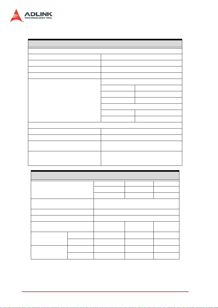
1.3 Specifications
Digital I/O Specifications
Number of
Channels
Direction
(programmable)
Logic Level
(programmable)
Min. V
Input
Voltage
Output
Voltage
Driving capacity(max.) ±8 mA ±16 mA ±32 mA
Throughput
FIFO Size
Data Transfer
Clocking Modes
Trigger Source
Trigger Modes
Input impedance 10 KΩ
Input protection range -1 to 6 V
Output impedance 50 Ω
Power-up initial state Tri-State / All digital inputs
Output protection range -0.5 V to 3.8 V
Dimensions 168 mm x 112 mm (not including connectors)
Connectors 68-pin VHDCI female x1 SMB x2
Operating Temp. 0 to 55° C
Storage Temp. -20 to 70° C
Relative Humidity 5 to 95%, non-condensing
Max. V
Min. V
Max. V
IH
IL
OH
OL
1.8 V 2.5 V
1.2 V 1.6 V 2 V
0.63 V 0.7 V 0.8 V
1.6 V 2.3 V 3.1 V
0.2 V 0.2 V 0.2 V
Digital Input:
Maximum: 200 MByte/s (32-bits input @ 50 MHz) (data size≤250k
samples)
Sustained: 192 MByte/s (data size>250k samples) (Note* )
Digital Output:
Maximum: 200 MByte/s (32-bit output @ 50 MHz) (FIFO load mode,
max. 8k samples)
Sustained: 119.2 MByte/s (Note**)
Digital Input: 8k samples
Digital Output: 8k samples
Software Polling
Bus-mastering DMA with Scatter-Gather
Internal clock: max. 50 MHz
External clock: max. 100 MHz
Handshaking
Burst handshaking
Software
External Digital signal
Pattern match
Post trigger with re-trigger
Gate trigger
per group (8 channel) basis
32
Input or output,
(5 V compatible)
3.3 V
2 Introduction
Page 13
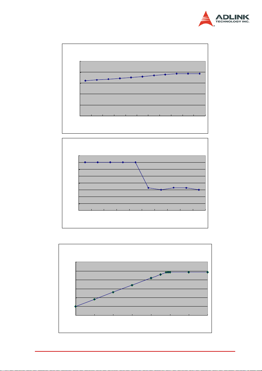
Note*: DI DMA throughput
DI DMA Bandwidth Test
160
164
168
172
176
180
184
188
192
192.7058
192.7138
0
50
100
150
200
250
40 41 42 43 44 45 46 47 48 49 50
External Clock Rate (MHz)
BW (MB/s)
DI DMA Bandwidth T est
200 200 200 200 200
192.58
192.01
192.64
192.56
191.98
186
188
190
192
194
196
198
200
202
50 100 150 200 250 300 350 400 450 500
Data Count (K samples)
BW (MB/s)
DO DMA Bandwidth Test
100
118
116
112
108
104
119.32
119.28
119. 2
119.34
119.32
95
100
105
110
115
120
125
25 26 27 28 29 30 31 32
Clock Rate (MHz)
BW (MB/s)
Note**: DO DMA throughput
Introduction 3
Page 14
If you want to have DO throughput to be up to 200M Byte/s, the
data size is limited to less than the 8K FIFO size by the following
steps:
Step1: Read 8K DO data from system memory into DO FIFO
by DMA before writing 8K DO data from DO FIFO to
the external device
Step2: After 8K DO data are all stored into DO FIFO, and
then start writing these 8K DO data to the external
device with 50MHz DO sample clock rate and 32-bit
data width.
External clock rate can be up to 100 MHz, but only support 8 or
16-bit data width because the DI data throughput can’t exceed 200
MB/s
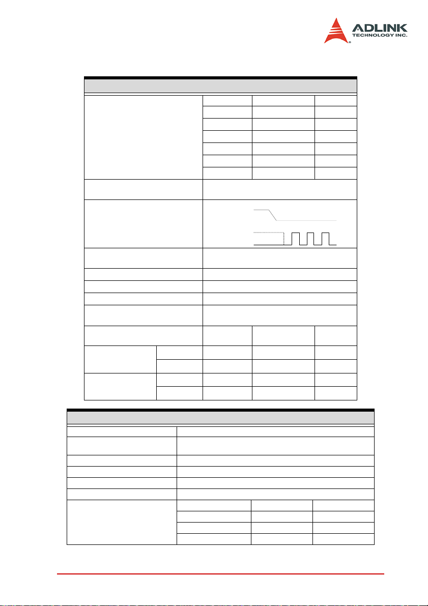
Application Function I/O (AFI)
Number of channels 8
Direction
(programmable)
Logic Levels
(programmable)
Min. V
Max. V
Min. V
Max. V
IH
IL
OH
OL
Input
Voltage
Output
Voltage
Driving capacity (max.) ±8 mA ±16 mA ±32 mA
Input impedance 10 KΩ
Input protection range -1 to 6 V
Output impedance 50 Ω
Power-up initial state Tri-State / All digital inputs
Output protection range -0.5V to 3.8V
Supported Mode
(programmable)
1.8 V 2.5 V
1.2 V 1.6 V 2 V
0.63 V 0.7 V 0.8 V
1.6 V 2.3 V 3.1 V
0.2 V 0.2 V 0.2 V
2
I
C master
SPI master
Handshaking
External trigger in/out
DI/DO sample clock in/out
Input or output,
per channel basis
3.3 V
(5 V Compati-
ble)
4 Introduction
Page 15
Timing Specifications
Sample Clock
Internal clock: on-board 100MHz with 16-bit divider
Clock Sources
Internal Clock Rate
(programmable)
Ext. frequency range
Phase shift
Sample Clock Exporting
Destination
Frequency range
Clock jitter Period jitter: 160 ps
Clock duty cycle 50%
Phase shift resolution
External clock: 1. AFI6 (for DO)
0 - 100 MHz (no phase shift)
2 MHz - 50MHz (phase shift enabled)*
Internal clock: N/A
External clock: 16 steps; 1 step = 22.5°
1. AFI6 (only for DO)
2. AFI7 (only for DI)
3. SMB CLK out
0 ~ 50 MHz (no phase shift)
2 MHz ~ 50MHz (phase shift enabled) (note3)
1/16 of external sampled clock period
2. AFI7 (for DI)
3. SMB CLK in
1526 Hz – 50 MHz
(100 MHz/ N; 2≤N≤65,535)
(16 steps; 1 step = 22.5°)
When you enable phase shift, the clock must be continuous and
free-running
Timing Accuracy
Acquisition Timing
Channel-to-Channel skew ±1.08 ns
Setup time to sampled clock (t
Hold time to sampled clock (t
Time delay of external sampled clock
from AFI7 to internal (t
Time delay of external sampled clock
from SMB CLK in to internal (t
Time delay of DI data from VHDCI
connector to internal (t
Generation Timing
Exported Clock SkewAFI6 -to- SMB
CLK out(t
Exported Clock (AFI6) -to- DO Data
Delay (t
ECskew
AF62D
)
AF7D
DID
)
)
SU
)
H
)
)
SMBID
)
2 ns
2 ns
7.22 ns
8.02 ns
3.26 ns - 4.34 ns
3.24 ns
600 ps - 5 ns
Introduction 5
Page 16
DI Sampled Clock
(AFI7)
t
AF7D
= Time delay of external sampled clock from AFI7 to internal
t
DID
= Time delay of DI data from VHDCI connector to internal
D0 D1 D2 D3
t
AF7D
Trace & component delay
D0 D1 D2 D3
t
DID
DI Data
(connector)
DI Sampled Clock
(into FPGA)
DI Data
(into FPGA)
tSUt
H
Figure 1-1: Acquisition Timing Diagram
6 Introduction
Page 17
D0
DO Sampled Clock
(internal)
DO Data
Write data to
external device
t
SC2AF6
= Time delay from sampled clock (internal) to exported sampled clock (AFI6)
t
AF62D
= Time delay from exported sampled clock (AFI6) to do data
Exported DO Sampled Clock
(AFI6/ non-inverted)
t
SC2AF6
Exported DO Sampled Clock
( AFI6/ inverted)
Exported DO Sampled Clock
(AFI6/ phase delay)
Phase delay (0° ~ 360°)
D1 D2
t
AF62D
Gerenation start
t
ECskew
t
ECskew
= Time delay from exported clock (AFI6) to exported clock (SMB CLK out)
Exported DO Sampled Clock
(SMB CLK out/ non-inverted)
Trace & component delay
Introduction 7
Figure 1-2: Generation Timing Diagram
Page 18
External Clock I/O Specification
CLK IN (SMB Jack Connector)
Destination DI or DO sample clock
Input coupling AC
Input Impedance 50 Ω
Minimum detectable pulse width 8 ns
Square Wave
Voltage 0.2 Vpp to 5 Vpp
Frequency 100 KHz - 50 MHz
External sampled clock range
CLK OUT (SMB Jack Connector)
Sources DI or DO sample clock
Source impedance 50 Ω
Logic Levels
(programmable)
Driving Capacity (Max.)
I2C Master Specification
Signal
Supported clock rate
(programmable)
Transfer size of Data 0 - 4 Bytes
Transfer size of Cmd/ Addr 0 - 4 Bytes
Logic families
(programmable)
Min. V
Input Voltage
Output Voltage
Max. V
Min. V
Max. V
IH
IL
OH
OL
Duty cycle 40% - 60%
Sine Wave
Voltage 0.2 Vpp to 5 Vpp
Frequency 100 KHz – 50 MHz
The same logic level of AFI I/O
(1.8 V, 2.5 V, or 3.3 V)
±8 mA at 1.8 V
±16 mA at 2.5 V
±32 mA at 3.3 V
Direction Pin
SCL O AFI0
SDA I/O AFI1
1.9 kHz -244.14 kHz;
488.28125 kHz / (n + 1); 1 ≤ n ≤ 255
1.8 V 2.5 V 3.3 V
1.2 V 1.6 V 2.0 V
0.63 V 0.7 V 0.8 V
1.6 V 2.3 V 3.1 V
0.2 V 0.2 V 0.2 V
8 Introduction
Page 19
CS#
SCK
Mode =1
Mode =0
Signal
Supported clock rate
(programmable)
Clock mode
SPI Master Specification
SCK O AFI0
SDO O AFI1
SDI I AFI2
CS_0 O AFI3
CS_1 O AFI4
CS_2 O AFI5
244.14 kHz -62.5 MHz,
62.5 MHz / (n + 1); 0 ≤ n ≤ 255
Direction Pin
The first bit be transferred
MSB/ LSB
(Default: MSB)
Transfer size of Data 0 - 32 bits
Transfer size of Cmd/ Addr 0 - 32 bits
Dummy size 0 - 15 bits
SPI Slave selection
Logic families
(programmable)
Min. V
Input Voltage
Output Voltage
Interface x1 PCI Express interface
Connector
Operation Temperature 0°C - 45°C
Storage Temperature -20°C - 70°C
Humidity 5 - 95%, non-condensing
Dimension 168 mm (L) x 112 mm (H), not including connectors
Power Consumption
IH
Max. V
IL
Min. V
OH
Max. V
OL
General Specification
1. SMB Jack Connector x2 (CLK IN & OUT)
2. 68-pin SCSI-VHDCI x1 (32-bit Data Lines & 8-ch AFI)
+3.3 VDC 450 mA 780 mA
+12V VDC 625 mA 680 mA
Total Power 9 W 10.8 W
Max. 3 slave devices
(selected by CS_0 / CS_1 / CS_2
1.8 V 2.5 V 3.3 V
1.2 V 1.6 V 2 V
0.63 V 0.7 V 0.8 V
1.6 V 2.3 V 3.1 V
0.2 V 0.2 V 0.2 V
Typical Maximum
Introduction 9
Page 20

1.4 Software Support
ADLINK provides versatile software drivers and packages for
users’ different approach to building up a system. ADLINK not only
provides programming libraries such as DLL for most Windows
based systems, but also provide drivers for other software packages such as LabVIEW®.
All software options are included in the ADLINK CD. Non-free software drivers are protected with licensing codes. Without the software code, you can install and run the demo version for two hours
for trial/demonstration purposes. Please contact ADLINK dealers
to purchase the formal license.
1.4.1 Programming Library
For customers who are writing their own programs, we provide
function libraries for many different operating systems, including:
PCIS-DASK: Include device drivers and DLL for Windows
98/NT/2000/XP/Vista. DLL is binary compatible across
Windows 98/NT/2000/XP/Vista. This means all applications
developed with PCIS-DASK are compatible across Windows 98/NT/2000/XP/Vista. The developing environment
can be VB, VC++, Delphi, BC5, or any Windows programming language that allows calls to a DLL. The user’s guide
and function reference manual of PCIS-DASK are in the
CD.
(\\Manual\Software Package\PCIS-DASK)
10 Introduction
Page 21
2 Hardware Information
167 .65
169 .65
100.36
126.37
(4.5)
111.15
CN1
CN2
CN3
CN4
JP1
U1
CN5
CN6
LED5
LED6
T1
U12
U23
U24
U25
U6
U50
U7
U18
U22
U17
U21
U16
U20
U15
U19
U41 U43 U4 4
U44
U38
U39
U51
U52
U14 U13 U11
U9 U8 U11
LED1
LED2
U46
U36 U33
U35
OSC 1
SW1
U3 U4
U28 U30
C248
U47
U40
U26
U31
U29
U32
L23
C190
Q3
U27
C189
C195
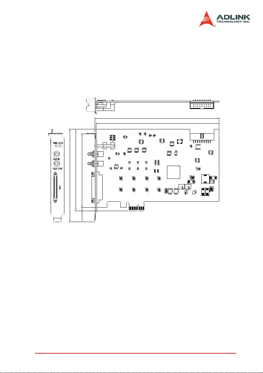
This chapter provides information on the PCIe-7350 layout, connectors, and pin assignments.
2.1 Card Layout
Figure 2-1 shows the PCIe-7350 board layout and dimensions.
Figure 2-1: PCB Layout and Mechanical Drawing of the PCIe-7350
Hardware Information 11
Page 22
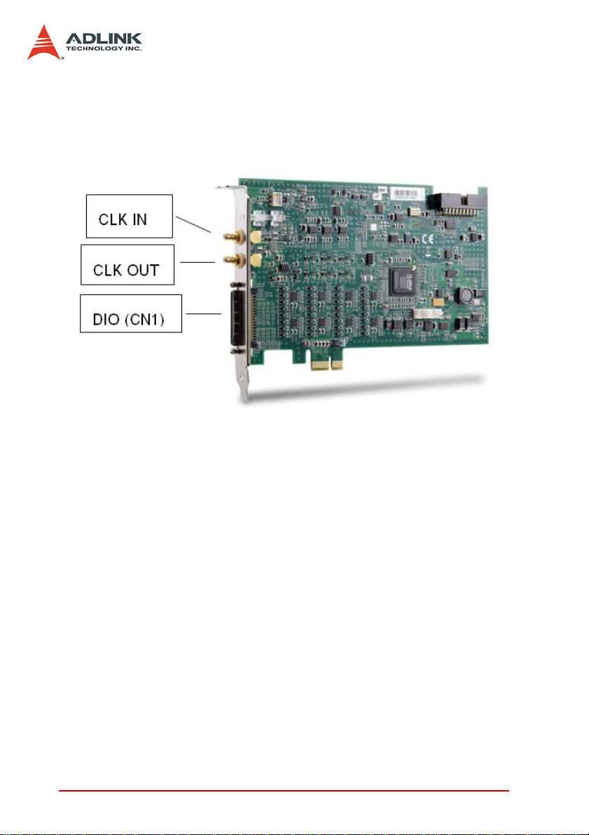
2.2 Connector Pin Assignment
The PCIe-7350 card is equipped with one 68-pin SCSI-VHDCI
connector and two SMB connectors. The SCSI-VHDCI connector
is for high-speed digital I/O and programmable function I/O, while
the SMB connectors are for sample clock input or exporting.
12 Hardware Information
Page 23
Pin # Pin #
GND 68 34 GND
(DI CLK) AFI7 67 33 AFI6 (DO CLK)
GND 66 32 GND
D0 65 31 D1
AFI5 64 30 AFI4
D2 63 29 D3
GND 62 28 GND
D4 61 27 D5
AFI3 60 26 AFI2
D6 59 25 D7
GND 58 24 GND
D8 57 23 D9
GND 56 22 GND
D1055 21D11
GND 54 20 GND
D1253 19D13
AFI1 52 18 GND
D1451 17D15
GND 50 16 GND
D1649 15D17
GND 48 14 GND
D1847 13D19
GND 46 12 GND
D20 45 11 D21
GND 44 10 GND
D22 43 9 D23
GND 42 8 AFI0
D24 41 7 D25
GND 40 6 GND
D26 39 5 D27
GND 38 4 GND
D28 37 3 D29
GND 36 2 GND
D30 35 1 D31
Table 2-1: Connector CN1 Pin Assignment
Hardware Information 13
Page 24
Signal Descriptions
Below are the signal descriptions for the SCSI-VHDCI and SMB
connectors:
Pin
Number
25, 27, 29, 31, 59,
61, 63, 65
17, 19, 21, 23, 51,
53, 55, 57
9, 11, 13, 15, 43,
45, 47, 49
1, 3, 5, 7, 35, 37,
39, 41
8, 26, 30, 52, 60,
64
33 AFI6
67 AFI7
2, 4,6, 10, 12, 14,
16, 18,20, 22, 24,
28, 32, 34, 36, 38,
40, 42, 44, 46, 48,
50, 54, 56, 58, 62,
66, 68
Signal
Name
D0 – D7 Data I/O Port_A bi-directional digital data lines
D8 – D15 Data I/O Port_B bi-directional digital data lines
D16 – D23 Data I/O Port_C bi-directional digital data lines
D24 – D31 Data I/O Port_D bi-directional digital data lines
AFI0 – AFI5
GND Ground -------- Ground reference for Data I/O and AFI I/O
Signal
Type
Control
/Data
Control
/Data
Control
/Data
Direction Description
Application Function I/O, can be configured as the following control signals:
I
I/O
Handshaking signal
External trigger in/out
Event out
Application Function I/O, can be configured as the following control signals:
Handshaking signal
I/O
External trigger in/out
Event out
DO sampled clock in/out
Application Function I/O, can be configured as the following control signals:
Handshaking signal
I/O
External trigger in/out
Event out
DI sampled clock in/out
Table 2-2: I/O Signal Descriptions
SMB Jack Connector Signal Description
2
C/ SPI
Signal Name Signal Type Direction Description
CLK IN Clock I
CLK OUT Clock O
External clock input for DI/DO sampled clock from
external device to the PCIe-7350
DI/DO sampled clock exporting from the PCIe-7350 to
an external device
Table 2-3: SMB Jack Connector Signal Descriptions
14 Hardware Information
Page 25
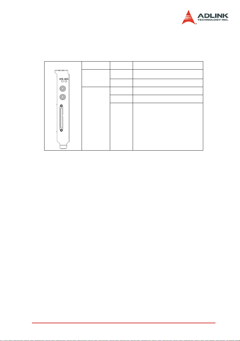
2.3 LED indicator
There are two LEDs on the bracket which display the I2C & SPI
communication and digital I/O status of the PCIe-7350.
LED Color Mode
2
I
C mode enabled
STS
(Status)
ACC
(Access)
Table 2-4: LED indicator
Red
Yellow SPI mode enabled
Red DI DMA operation
Yellow DO DMA operation
Amber DI & DO DMA operation
Hardware Information 15
Page 26

2.4 Installing the Card
IMPORTANT Install the card driver before you install the card into
your computer system. Refer to section 1.5 for driver support information.
To install the card:
1. Turn off the system/chassis and disconnect the power
plug from the power source.
2. Remove the system/chassis cover.
3. Select the PCI Express slot that you intend to use, then
remove the bracket opposite the slot, if any.
4. Align the card connectors (golden fingers) with the slot,
then press the card firmly until the card is completely
seated on the slot.
5. Secure the card to the chassis with a screw.
6. Replace the system/chassis cover.
7. Connect the power plug to a power source, then turn on
the system.
Configuration
The card configuration is done on a card-by-card basis for all PCI/
PCI Express cards on your system. Because configuration is controlled by the system and the software, there is no jumper setting
required for base address, DMA, and interrupt IRQ. The configuration is subject to change with every boot of the system as new
PCI/PCI Express® cards are added or removed.
Troubleshooting
If your system fails to boot or if you experience erratic operation
with your PCI/PCI Express card in place, this is likely caused by
an interrupt conflict (such as when the BIOS Setup is incorrectly
configured). Refer to the BIOS documentation that came with the
system for details.
16 Hardware Information
Page 27

2.5 Unpacking Checklist
Before unpacking, check the shipping carton for any damage. If
the shipping carton and/or contents are damaged, inform your
dealer immediately. Retain the shipping carton and packing materials for inspection. Obtain authorization from your dealer before
returning any product to ADLINK. Check if the following items are
included in the package.
PCIe-7350 high-speed DIO card
ADLINK All-in-One CD
User’s manual
If any of the items is damaged or missing, contact your dealer
immediately.
CAUTION The card must be protected from static discharge and
physical shock. Never remove any of the socketed parts except at
a static-free workstation. Use the anti-static bag shipped with the
product to handle the card. Wear a grounded wrist strap when servicing.
2.6 Cables and Termination board
The PCIe-7350 is a high-speed digital I/O card. The impedance
matching is very important to the high-speed application for eliminate the signal reflection generated by the cable or PCB trace.
The following cable and termination board is recommended to
improve the signal quality during high-speed signal transfer.
DIN-68H – Termination board with one 68-pin SCSI-VHDCI con-
nector and user selectable impedance. Refer to Appendix A for
more information.
ACL-10279 – 68-pin SCSI-VHDCI cable with 50Ω impedance
SMB-SMB-1M – SMB to SMB cable, 1 M, for sample clock in/out
SMB-BNC-1M – SMB to BNC cable, 1 M, for sample clock in/out
Hardware Information 17
Page 28

18 Hardware Information
Page 29

3 Function Block and Operation Theory
The operation theory of the PCIe-7350 card is described in this
chapter. These functions include high-speed digital pattern acquisition, digital pattern generation, application function I/O, and etc.
The operation theory can help you understand how to configure
and operate the PCIe-7350 card.
Function Block and Operation Theory 19
Page 30

3.1 Block Diagram
There are 32-channel bi-direction high-speed digital I/O lines, 8channel AFI (Application Function I/O) lines, and two sample clock
input/output channels available on the PCIe-7350 card. All the 32channel high-speed digital I/O lines are connected to level shifter,
Fairchild FXL4245 and can be programmed as 1.8 V, 2.5 V, or 3.3
V (5 V compatible) logic levels. These channels can be also programmed as input channels for digital pattern acquisition or output
channels for digital pattern generation.
The 8-channel application function I/O lines are connected to level
shifter, Fairchild FXL2T245, too. These application function I/O
can be programmed as I2C or SPI serial interface, handshaking
interface, external digital trigger input, event output and external
clock input/output with 1.8 V or 2.5 V or 3.3 V (5 compatible) logic
levels by direction and logic level control of level shifter and by AFI
controller implemented in FPGA.
The digital pattern acquisition/generation and corresponding flexible sample timing are controlled by ADLINK Smart Control Engine
implemented by FPGA. Please refer to Figure 3-1 PCIe-7350
block diagram.
Figure 3-1: PCIe-7350 Block Diagr am
20 Function Block and Operation Theory
Page 31

3.2 Programmable Logic Level
To interface different logic level applications, the PCIe-7350 supports three software selectable logic levels of 1.8 V, 2.5 V, or 3.3 V
(5 V compatible) for all digital I/O lines, sample clocks, I
triggers, and events. When you choose one of these three logic
levels, all the I/O lines will be at the same logic level you choose.
Below are the definition and high/low range for different logic levels. When connecting PCIe-7350 to a device under test (DUT),
you must ensure that the interface voltage levels are compatible.
V
: The digital input voltage at logic high; senses a binary
IH
one (1)
V
: The digital input voltage at logic low; senses a binary
IL
zero (0)
V
: The digital output voltage at logic high; generates a
OH
binary one (1)
V
: The digital output voltage at logic low; generate a
OL
binary zero (0)
2
C, SPI,
Logic Levels 1.8 V 2.5 V
Digital Input
Digital Output
Function Block and Operation Theory 21
Min. VIH 1.2 V 1.6 V 2 V
Max. VIL 0.63 V 0.7 V 0.8 V
Min. VOH 1.6 V 2.3 V 3.1 V
Max. VOL 0.2 V 0.2 V 0.2 V
Table 3-1: PCIe-7350 Logic Levels
3.3 V
(5 V compatible)
Page 32

3.3 Digital I/O Configuration
The 32-channel high-speed digital I/O lines are bi-direction and
divided into four groups. Each group contains 8 channels and can
be configured as input port or output port individually. At power-up
status, all the I/O lines are preset to input ports. When configuring
to digital output mode, the initial status of digital outputs are in tristate. The possible configuration modes are as follows:
Port Channel Power-up status Direction
Port A D0 ~ D7 Input Input or output
Port B D8 ~ D15 Input Input or output
Port C D16 ~ D23 Input Input or output
Port D D24 ~ D31 Input Input or output
Table 3-2: PCIe-7350 High-Speed Digital I/O Configuration
22 Function Block and Operation Theory
Page 33

3.3.1 DI Row Data Mapping
For digital pattern acquisition, the data width can be configured to
8-bit, 16-bit, 24-bit, or 32-bit and the data transfer is based on 32bit data width. Below is the mapping table for different DI port combination.
Data Width Input Ports Row Data Mapping
D C B A Refer to Figure 3-2
8 bits
16 bits
24 bits
32 bits DCBA Refer to Figure 3-5
DCB A Refer to Figure 3-2
D C BA Refer to Figure 3-2
D CBA Refer to Figure 3-2
DCBA Refer to Figure 3-3
D C B A Refer to Figure 3-3
D CBA Refer to Figure 3-3
D CBA Refer to Figure 3-3
D C B A Refer to Figure 3-3
DCBA Refer to Figure 3-3
D CBA Refer to Figure 3-4
D C BA Refer to Figure 3-4
DCB A Refer to Figure 3-4
DCBA Refer to Figure 3-4
Function Block and Operation Theory 23
Page 34

CH7 ~ CH0
(sample #1)
CH7 ~ CH0
(sample #2)
CH7 ~ CH0
(sample #3)
CH7 ~ CH0
(sample #4)
CH15 ~ CH8
(sample #1)
CH15 ~ CH8
(sample #2)
CH15 ~ CH8
(sample #3)
CH15 ~ CH8
(sample #4)
CH23 ~ CH16
(sample #1)
CH23 ~ CH16
(sample #2)
CH23 ~ CH16
(sample #3)
CH23 ~ CH16
(sample #4)
CH31 ~ CH24
(sample #1)
CH31 ~ CH24
(sample #2)
CH31 ~ CH24
(sample #3)
CH31 ~ CH24
(sample #4)
Configured
input ports
A
BCD
A
B
CD
AB
C
D
ABC
D
Configured
input ports
Configured
input ports
Configured
input ports
Figure 3-2: DI Row Data Mapping for 8 Bits Data Width
24 Function Block and Operation Theory
Page 35

CH15 ~ CH0
(sample #1)
CH7 ~ CH0CH23 ~ CH16
Configured
input ports
AB
CD
A
B
C
D
A
BC
D
A
BC
D
Configured
input ports
Configured
input ports
Configured
input ports
CH15 ~ CH0
(sample #2)
CH23 ~ CH8
(sample #1)
CH23 ~ CH8
(sample #2)
A
B
C
D
Configured
input ports
(sample #1)
CH7 ~ CH0CH23 ~ CH16
(sample #2)
CH7 ~ CH0CH31 ~ CH24
(sample #1)
CH7 ~ CH0CH31 ~ CH24
(sample #2)
CH15 ~ CH8CH31 ~ CH24
(sample #1)
CH15 ~ CH8CH31 ~ CH24
(sample #2)
AB
CD
Configured
input ports
CH31 ~ CH16
(sample #1)
CH31 ~ CH16
(sample #2)
Figure 3-3: DI Row Data Mapping for 16 Bits Data Width
Function Block and Operation Theory 25
Page 36

CH23 ~ CH0
(sample #1)
CH7 ~ CH0
(sample #2)
CH15 ~ CH0CH31 ~ CH24
CH7 ~ CH0
(sample #2)
CH7 ~ CH0
CH7 ~ CH0
(sample #2)
CH15 ~ CH8
(sample #2)
Configured
input ports
ABC
D
AB
C
D
A
B
CD
A
BCD
Configured
input ports
Configured
input ports
Configured
input ports
(sample #1)
CH31 ~ CH16
(sample #1)
CH31 ~ CH8
(sample #1)
ABCD
Configured
input ports
CH31 ~ CH0
(sample #1)
Figure 3-4: DI Row Data Mapping for 24 bits Data Width
Figure 3-5: DI Row Data Mapping for 32 Bits Data Width
26 Function Block and Operation Theory
Page 37

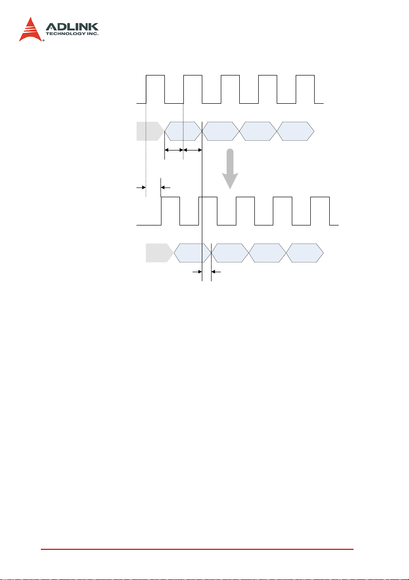
3.4 Phase Shift of Sample Clock
Acquisition of Digital Data
External
sampled clock
(from DUT)
DI Data
(from DUT)
Generation of Digital Data
Exported
sampled clock
(to DUT)
DO Data
(to DUT)
D0 D1 D2 D3
D0 D1 D2 D3
D0 D1 D2 D3
D0 D1 D2 D3
16 steps phase shift
16 steps phase shift
PCIe-7350 Card
Valid area
Transition area
Valid area Transition area
PCIe-7350 features phase shift of sample clock (on SMB connector or AFI6 & AFI7 of SCSI-VHDCI connector). The sample clock
can be from external DUT or can be the exporting clock generated
from internal time base. The resolution of phase shift is 4-bit (16
steps) implemented by Phase-Locked Loop (PLL) function of
FPGA. In other words, the phase shift of sample clock is 22.5° x N,
where N is any integer from 1 to 15. Furthermore, in phase shifting
mode, the supported clock frequency is from 2 MHz to 50 MHz.
This function can optimize the timing of digital pattern acquisition
or generation to avoid sampling/exporting the data from/to DUT at
transition state. Therefore, for digital input, the data can be sampled in clean and valid timing instead of transition timing. For digital output, it can fine tune the exporting clock to avoid the sampling
of DUT at setup time or hold time instead of aligning the data.
Figure 3-6: Phase Shift of Sample Clock
Function Block and Operation Theory 27
Page 38

Value
Revolution 16 steps (1 step = 22.5°)
Supported
Frequency Range
Supported CLK
Table 3-3: Phase Shift Configuration of PCIe-7350
User can shift the clock phase ofthe following clock:
External DI sample clock (from SMB CLK IN or AFI7)
External DO sample clock (from SMB CLK IN or AFI6)
Exported DI sample clock (from SMB CLK IN or AFI7)
Exported DO sample clock (from SMB CLK IN or AFI6)
2MHz ~ 50MHz
28 Function Block and Operation Theory
Page 39

3.5 Bus-mastering DMA Data Transfer
System
Memory
NB
Chipset
120MB/s 250MB/s
PC Main-board
PCI-Express
IP Core
8K
FIFO
500MB/s 200MB/s
DUT
PCIe-7350
Digital I/O data transfer between PCIe-7350 and PC’s system
memory is through bus mastering DMA, which is controlled by
PCIe IP Core.
Figure 3-7: Maximum Data Throughput of the PCIe-7350
The bus-mastering controller controls the PCI/PCIe bus when it
becomes the master of the bus. Bus mastering reduces the size of
the on-board memory and reduces the CPU loading because data
is directly transferred to the computer’s memory without host CPU
intervention.
Bus-mastering DMA provides the fastest data transfer rate on PCIbus. Once the analog/digital input operation starts, control returns
to your program. The hardware temporarily stores the acquired
data in the on-board Data FIFO and then transfers the data to a
user-defined DMA buffer memory in the computer. Please note
that even when the acquired data length is less than the Data
FIFO, the data will not be kept in the Data FIFO but directly transferred into host memory by the bus-mastering DMA.
The DMA transfer mode is very complex to program. We recommend using a high-level program library provided by our driver to
configure this card. By using a high-level programming library for
high speed DMA data acquisition, users simply need to assign the
sampling period and the number of conversion into their specified
counters. After the trigger condition is matched, the data will be
transferred to the system memory by the bus-mastering DMA.
The PCI/PCIe controller also supports the function of scatter/
gather bus mastering DMA, which helps the users to transfer large
amounts of data by linking all the memory blocks into a continuous
linked list.
Function Block and Operation Theory 29
Page 40

In a multi-user or multi-tasking OS, like Microsoft Windows, Linux,
and so on, it is difficult to allocate a large continuous memory
block to do the DMA transfer. Therefore, the PCI/PCIe controller
provides the function of scatter -gather or chaining mode DMA to
link the non-continuous memory blocks into a linked list so that
users can transfer very large amounts of data without being limited
by the fragment of small size memory. Users can configure the
linked list for the input DMA channel or the output DMA channel.
Figure 4.7 shows a linked list that is constructed by three DMA
descriptors. Each descriptor contains a PCI/PCIe address, PCI/
PCIe dual address, a transfer size, and the pointer to the next
descriptor. PCI/PCIe address and PCI/PCIe dual address support
64-bit addresses which can be mapped into more than 4GB of the
address space. Users can allocate many small size memory
blocks and chain their associative DMA descriptors altogether by
their application programs. The software driver provides simple
settings of the scatter-gather function, and some sample programs
are also provided within the ADLINK all-in-one CD.
Figure 3-8: Scatter-Gather DMA for Data Transfer
Choose Finite or Continuous Operation
You can transfer data continuously to or from computer memory
(continuous operation), or you can specify the number of samples
you want to transfer (one-shot operation). In either case, the PCIe7350 transfers the data using direct memory access (DMA) without occupying CPU resources.
30 Function Block and Operation Theory
Page 41

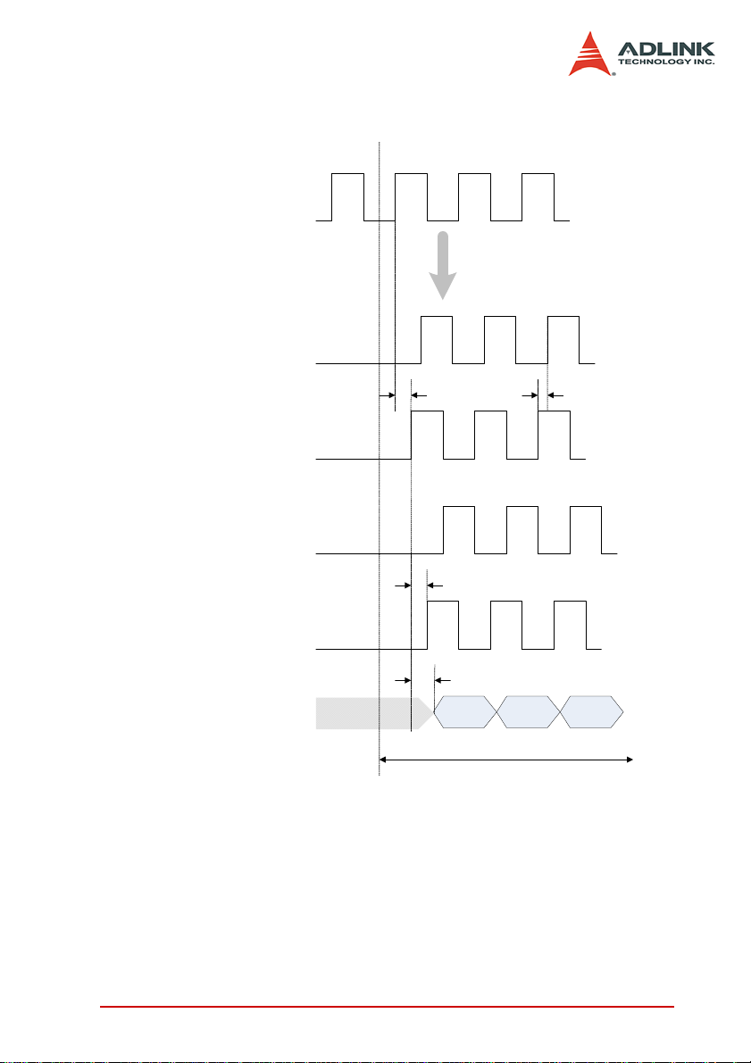
3.6 Sample Clock
The sample clock controls the data rate of digital pattern acquisition and generation. For PCIe-7350, the sample clock can be configured from internal timer pacer or external clock through the
SMB connectors or SCSI-VHDCI connector.
3.6.1 Digital Input (DI) Sample Clock
For the operation of digital pattern acquisition in continuous mode
or burst handshaking mode, the PCIe-7350 card can acquire digital data from external devices at a specific sampling rate (DI sample clock). DI sample clock can be selected as the following two
clock sources:
Internal DI sample clock – the PCIe-7350 can internally
generate the sample clock signal for digital data acquisition.
With an internal base clock source of 100 MHz, the PCIe7350 can generate any clock frequency of 100 MHz/n,
where n is any integer from 2 to 65535.
External DI sample clock – the PCIe-7350 can receive
external clock signal from AFI7 or SMB CLK as the DI sample clock for synchronization applications.
In addition, the PCIe-7350 can also export DI sample clock to
external devices through AFI7 pin or SMB CLK connector.
Function Block and Operation Theory 31
Page 42

3.6.2 Digital Output (DO) Sample Clock
For the operation of digital pattern generation in continuous mode
or burst handshaking mode, PCIe-7350 card can generate digital
data to external devices at a specific update rate (DO sample
clock). DO sample clock can be selected as the following two
clock sources:
Internal DO sample clock – the PCIe-7350 can internally
generate the sample clock signal for digital data generation.
With an internal clock source of 100MHz, the PCIe-7350
can generate any clock frequency of 100 MHz/n, where n is
any integer from 2 to 65535.
External DO sample clock – the PCIe-7350 can receive an
external sample clock signal from AFI6 or SMB CLK connector as the DO sample clock for synchronization applications.
In addition, the PCIe-7350 can also export DO sample clock to
external devices through AFI6 pin or SMB CLK connector. Figure
3-8 shows the DI/DO sample clock architecture of PCIe-7350.
32 Function Block and Operation Theory
Page 43

16 steps
phase shift
I
AFI7
1/N
DI CLK
Mux
Int. DI sampled clk
16 steps
phase shift
DI Sampled CLK
Acquisition
Engine
Int. Timebase
Ext. DI sampled clk
SMB CLK out
I
AFI6
Ext. DO CLK
Mux
Ext. DI CLK
Mux
Export. DI/DO CLK
Mux
Export. DI CLK
Mux
16 steps
phase shift
AFI6
O
Export. DO CLK
Mux
DO sampled clk
SMB CLK in
DO CLK
Mux
16 steps
phase shift
Int. DO sampled clk
1/N
DO Sampled CLK
Gereration
Engine
Ext. DO sampled clk
O
AFI7
100MHz
DI sampled clk
Figure 3-9: DI/DO Sample Clock Architecture
Function Block and Operation Theory 33
Page 44

DI Sample CLK DO Sample CLK
Internal
clock
External
clock
Sample
clock
exporting
Table 3-4: DI/DO Sample Clock Configuration of the PCIe-7350
Source
Freq.
Source
Freq. 0 – 100 MHz 0 – 100 MHz
Freq.
(phase shift)
Destination
Freq. 0 – 50 MHz 0 – 50 MHz
Freq.
(phase shift)
On-board 100 MHz
oscillator
100 MHz/n
(n = 2~65535)
AFI7
SMB CLK in
2 MHz – 50 MHz 2 MHz – 50 MHz
AFI7
SMB CLK out
2 MHz – 50 MHz 2 MHz – 50 MHz
On-board 100 MHz
oscillator
100 MHz/n
(n = 2~ 65535)
AFI6
SMB CLK in
AFI6
SMB CLK out
34 Function Block and Operation Theory
Page 45

3.7 Operation Mode
The PCIe-7350 supports four different modes for acquisition and
generation operation, including software polling, continuous,
handshaking, and burst handshaking mode..
3.7.1 Polling Mode (Single Read/Write)
The PCIe-7350 supports a software polling mode to read or write a
single chunk of data via a software command. That is, the 32-bit
high-speed I/O lines can be used as a static I/O. The data width
can be 8-bit, 16-bit, 24bit, or 32-bit.
3.7.2 DI DMA in Continuous Mode
For the DI pattern acquisition operation in continuous mode, PCIe7350 card can acquire input data from external devices at a specific sampling clock rate (DI sampled clock). DI sample clock can
be selected from internal or external clock source. The operation
sequences are listed as follows:
Steps:
Define DI port configuration (32/24/16/8-bits data width)
Define DI logic level configuration (3.3/2.5/1.8 V)
Define DI sample clock configuration (internal/external)
If choose internal sampled clock, you can define sam-
pling clock rate to be 100MHz/n (n = 2~65535)
If choose external sampled clock, the phase shift func-
tion is available when external clock is a free-running
clock (not a strobe signal) and external clock rate is from
2 MHz ~ 50 MHz.
Define DI starting mode configuration (NoWait or WaitTRIG)
If choose WaitTRIG, you can define start trigger source
to be software trigger or external trigger (DI-Start) from
AFI0 ~ AFI7.
Define DI data count
Execute DI DMA Read Command (continuous mode)
Function Block and Operation Theory 35
Page 46

The operation architecture of DI DMA in continuous mode is
1/N
DI CLK
Mux
Int. DI sampled clk
16 steps
phase shift
Ext. DI sampled clk
Ext. DI CLK
Mux
Bus Master DMA
100MHz
8K FIFO Flip Flop
D[31:0]
I
AFI7
SMB CLK in
AFI[7:0]
DI sampled clk
Start Trigger
Mux
NoWait/
WaitTRIG
Software trigger DI-Start
PCIe-7350 Card
DI Data DI Data
External trigger in
External clock in
clk
enable
Software trigger out
shown as below:
Figure 3-10: DI Continuous Mode Architectu re
36 Function Block and Operation Theory
Page 47

The timing diagram of DI DMA in continuous mode is shown as
DO D1 D2 D3 D4 D5 D6
DI Sampled Clock
Start Trigger
DI Data
Read data into DI FIFO
Wait for
start trigger
t
H
t
SU
t
H
t
SU
t
H
t
SU
= Maximum required setup time
= Maximum required hold time
below:
Figure 3-11: DI Timing Diagram
Note: In the continuous mode of DI pattern acquisition, the input
data will be stored in the DI FIFO of the PCIe-7350. The data
then transfer to system memory by bus mastering DMA if
PCIe bus is available. If the speed of translation from external device to the DI FIFO on board is higher than that from
DI FIFO to system memory or the PCIe bus is busy for a long
time, the DI FIFO become full and the DI pattern acquisition
controller will stop to write data into DI FIFO until the DI FIFO
is not full. So the data will be lost when the DI FIFO is full.
Function Block and Operation Theory 37
Page 48

3.7.3 DO DMA in Continuous Mode
For the DO pattern generation operation in continuous mode,
PCIe-7350 card can generate digital data to external devices at a
specific update clock rate (DO sample clock). DO sample clock
can be selected from internal or external clock source. The operation sequences are listed as follows:
Steps:
Define DO port configuration (32/24/16/8-bits data width)
Define DO logic level configuration (3.3/2.5/1.8 V)
Define DO sample clock configuration (internal/external)
If choose internal sample clock, you can define sampling
clock rate to be 100MHz/n (n = 2~65535)
If choose external sample clock, the phase shift function
is available when external clock rate is 2MHz ~ 50MHz.
Define DO exporting sample clock configuration (AFI6/SMB
CLK out)
PCIe-7350 can also export DO sample clock to external
devices. The destination of DO sample clock exporting
can be AFI6 or SMB CLK out connector.
The phase shift function is available when exported
clock is a free-running clock and the clock rate is 2MHz ~
50MHz.
Define DO starting mode configuration (NoWait or Wait-
TRIG)
If choose WaitTRIG, you can define start trigger source
to be software trigger or external trigger (DO-Start) from
AFI0 ~ AFI7.
Define DO data count.
Execute DO DMA Write Command (continuous mode)
38 Function Block and Operation Theory
Page 49

The operation architecture of DO DMA in continuous mode is
1/N
DO CLK
Mux
Int. DO sampled clk
16 steps
phase shift
Ext. DO sampled clk
Ext. DO CLK
Mux
Bus Master DMA
100MHz
8K FIFO Flip Flop
D[31:0]
I
AFI6
SMB CLK in
AFI[7:0]
DO sampled clk
Start Trigger
Mux
NoWait/
WaitTRIG
Software trigger DO-Start
PCIe-7350 Card
DO Data DO Data
External trigger in
External clock in
clk
enable
16 steps
phase shift
O
AFI6
Export. DO CLK
Mux
SMB CLK out
Exported sampled
clock out
clk valid
Export
clk gate
Software trigger out
shown as below:
Figure 3-12: DO Continuous Mode Architecture
Function Block and Operation Theory 39
Page 50

The timing diagram of DO DMA in continuous mode is shown as
D0 D1 D2
DO Sampled Clock
Start Trigger
(DO-Start)
DO Data
Write data to
external device
Wait for
start trigger
t
W
t
W
= Minimum detectable trigger width
D3 D4
t
ET2D
t
ET2D
= Delay from external trigger to do data out (about 5 cycle)
Exported DO Sampled Clock
(falling edge)
Software Trigger out
(DO-SW)
t
IT2D
t
IT2D
= Delay from software trigger out to do data out (about 4 cycle)
below:
Figure 3-13: DO Timing Diagram
40 Function Block and Operation Theory
Page 51

3.7.4 DI DMA in Handshaking Mode
For the DI pattern acquisition operation in handshaking mode,
PCIe-7350 card can acquire input data from external devices by
handshaking data transfer through DI-REQ input signal and DIACK output signal of AFI interface. The operation sequences are
listed as follows:
Step1: Configuration
Define DI port configuration (32/24/16/8-bits data width)
Define DI logic level configuration (3.3/2.5/1.8V)
Define DI-REQ and DI-ACK signal (AFI0 ~ AFI7)
For example: if configure AFI3 as DI-REQ and AFI4 as
DI-ACK, and then you must connect the handshaking
signal (DI-REQ and DI-ACK) of external device to the
AFI3 and AFI4.
Define DI starting mode configuration (NoWait or WaitTRIG)
If choose WaitTRIG, you can define start trigger source
to be software trigger or external trigger (DI-Start or DITRIG) from AFI0 ~ AFI7.
Define DI data count
Step2: Execute DI DMA Read Command (handshaking mode)
After DI data is ready on device side, the peripheral device
strobe data into the PCIe-7350 by asserting a DI-REQ signal. (action_1)
The DI-REQ signal caused the PCIe-7350 to latch DI data
and store it into DI FIFO. (action_2)
The PCIe-7350 asserts a DI-ACK signal when it is ready for
another input. (action_3)
The action_1 to action_3 is repeated in handshaking
mode.
The DI data in the DI FIFO will be transferred into system
memory directly and automatically by bus mastering DMA.
Function Block and Operation Theory 41
Page 52

The operation architecture of DI DMA in handshaking mode is
Bus Master DMA
8K FIFO Flip Flop
D[31:0]
AFI[7:0]
Start Trigger
Mux
NoWait/
WaitTRIG
Software trigger
DI-Start or DI-TRIG
PCIe-7350 Card
DI Data DI Data
External trigger in
DI-REQ
enable
Software trigger out
DI-ACK
AFI[7:0]
clk
ack
DI-REQ
DI-ACK
shown as below:
Figure 3-14: DI Handshaking Mode Architecture
42 Function Block and Operation Theory
Page 53

The timing diagram of DI DMA in handshaking mode is shown as
DO D1 D2
DI -REQ
DI Data
Read data int o DI FI FO
Wait for
DI-REQ
t
H
t
SU
t
H
t
SU
= Maxi mum required se tup time
= Maxi mum required ho ld time
DI -ACK
t
1
t2t
3
t
1
≥
20 ns
t
2
≥
10 ns
t
3
≥
50 ns
below:
Figure 3-15: DI Handshaking Timing Diagram
Function Block and Operation Theory 43
Page 54

3.7.5 DO DMA in Handshaking Mode
For the DO pattern generation operation in handshaking mode,
PCIe-7350 card can generate output data to external devices by
handshaking data transfer through DO-REQ output signal and
DO-ACK input signal of AFI interface. The operation sequences
are listed as follows:
Step1: Configuration
Define DO port configuration (32/24/16/8-bits data width)
Define DO logic level configuration (3.3/2.5/1.8V)
Define DO-REQ and DO-ACK signal (AFI0 ~ AFI7)
For example: if configure AFI3 as DO-REQ and AFI4 as
DO-ACK, and then you must connect the handshaking
signal (DO-REQ and DO-ACK) of external device to the
AFI3 and AFI4.
Define DO starting mode configuration (NoWait or Wait-
TRIG)
If choose WaitTRIG, you can define start trigger source
to be software trigger or external trigger (DO-Start or
DO-TRIG) from AFI0 ~ AFI7.
Define DO write count
Step2: Execute DO DMA Write Command (handshaking mode)
The DO data saved in the system memory will be trans-
ferred to DO FIFO directly and automatically by bus mastering DMA.
After DO data are ready, DO-REQ signal is generated and
DO data are sent to the external device. (action_1)
After DO-ACK signal from external device is gotten
(action_2)
The action_1 to action_2 is repeated in handshaking
mode.
44 Function Block and Operation Theory
Page 55

The operation architecture of DO DMA in handshaking mode is
Bus Master DMA
8K FIFO Flip Flop
D[31:0]
AFI[7:0]
Start Trigger
Mux
NoWait/
WaitTRIG
Software trigger
DO-Start or DO-TRIG
PCIe-7350 Card
DO Data DO Data
External trigger in
DO-REQ
enable
Software trigger out
DO-ACK
AFI[7:0]
strobe out
ack
DO-REQ
DO-ACK
DO D1 D2
DO -REQ
DO Data
Write data to external device
DO -ACK
t2t
3
t
2
≥
40 ns
t
3
≥
50 ns
shown as below:
Figure 3-16: DO Handshaking Mode Architecture
The timing diagram of DO DMA in handshaking mode is shown as
below:
Figure 3-17: DO Handshaking Timing Diagram
Function Block and Operation Theory 45
Page 56

3.7.6 DI DMA in Burst Handshaking Mode
The burst handshaking mode is a fast and reliable data transfer
protocol. It has both advantage of handshaking mode and continuous mode.
In DI burst handshaking mode, DI-REQ signal will be active by
external device when it is ready to send DI data and sample clock.
And then DI-ACK signal will be generated by PCIe-7350 when it is
ready to receive DI data from external device.
External device should start to send DI data after it detect DI-ACK
signal is active. DI data transfer between PCIe-7350 and external
device should be continued when both DI-REQ and DI-ACK are
active. When DI FIFO of PCIe-7350 becomes almost full, DI-ACK
signal will be inactive. External device should stop to send DI data
and sample clock after it detects DI-ACK signal inactive. The operation sequences are listed as follows:
Step1: Configuration
Define DI port configuration (32/24/16/8-bits data width)
Define DI logic level configuration (3.3/2.5/1.8 V)
Define DI sample clock configuration (only external)
The phase shift function is available when external clock
is a free-running clock (not a strobe signal) and external
clock rate is from 2 MHz – 50 MHz.
Define DI-REQ and DI-ACK signal (AFI0 ~ AFI7)
For example: if configure AFI3 as DI-REQ and AFI4 as
DI-ACK, and then you must connect the handshaking
signal (DI-REQ and DI-ACK) of external device to the
AFI3 and AFI4.
Define DI starting mode configuration (NoWait or WaitTRIG)
If choose WaitTRIG, you can define start trigger source
to be software trigger or external trigger (DI-Start or DITRIG) from AFI0 ~ AFI7.
Define DI data count
46 Function Block and Operation Theory
Page 57

Step2: Execute DI DMA Read Command (burst handshaking
16 steps
phase shift
Ext. DI sampled clk
Ext. DI CLK
Mux
Bus Master DMA
8K FIFO Flip Flop
D[31:0]
I
AFI7
SMB CLK in
AFI[7:0]
DI sampled clk
Start Trigger
Mux
NoWait/
WaitTRIG
Software trigger DI-Start or DI-TRIG
PCIe-7350 Card
DI Data DI Data
External trigger in
External clock in
clk
enable
Software trigger out
DI-REQ
DI-ACK
DI-REQ
DI-ACK
DI-REQ
DI-ACK
DI CLK
Mux
mode)
PCIe-7350 will generate DI-ACK signal when it is ready to
receive DI data after DI-REQ signal is active.
External device starts to send DI data and DI sample clock
after DI-ACK signal is active.
PCIe-7350 starts to receive DI data and DI sample clock
from external device when DI-REQ and DI-ACK are all
active.
The DI data in the DI FIFO will be transferred into system
memory directly and automatically by bus mastering DMA.
The operation architecture of DI DMA in burst handshaking mode
is shown as below:
Figure 3-18: DI Burst Handshaking Mode Architecture
Function Block and Operation Theory 47
Page 58

The timing diagram of DI DMA in burst handshaking mode is
DO
DI Data
DI Sampled Clock
(from external)
DI -REQ
(Active High)
DI -ACK
(Active High)
D1 D2 D3 D9D7 D8
PCIe-7350 is ready to
receive DI data
External Device is ready to send DI data
DI data transfer starts
D5
PCIe-7350 is not ready
to receive DI data
Wait DI-REQ
asserted
Wait DI-ACK
asserted
DI data transfer stops
DI data transfer re-start
(DI FIFO is full)
(DI-REQ & DI-ACK
are all asserted)
(DI-ACK is de-asserted)
(DI-REQ & DI-ACK
are all asserted)
shown as below:
Figure 3-19: DI Burst Handshaking Timing Diagram
3.7.7 DO DMA in Burst Handshaking Mode
In DO burst handshaking mode, DO-REQ signal will be active by
PCIe-7350 when it is ready to send out DO data. And then DOACK signal should be generated by external device when it is
ready to receive DO data. Once DO-ACK is active, external device
has to keep DO-ACK active until its input buffer is almost full. The
operation sequences are listed as follows:
48 Function Block and Operation Theory
Page 59

Step1: Configuration
Define DO port configuration (32/24/16/8-bits data width)
Define DO logic level configuration (3.3/2.5/1.8 V)
Define DO sample clock configuration (internal/external)
If choose internal sampled clock, you can define sam-
pling clock rate to be 100 MHz/n (n = 2-65535)
If choose external sampled clock, the phase shift func-
tion is available when external clock rate is from 2 MHz 50 MHz.
Define DO exporting sample clock configuration (AFI6/SMB
CLK out)
The PCIe-7350 can also export DO sampled clock to
external devices. The destination of the exported DO
sampled clock can be AFI6 or SMB CLK out connector.
The phase shift function is available when exported
clock rate is from 2 MHz – 50 MHz.
Define DO-REQ and DO-ACK signal (AFI0 - AFI7)
For example: if configure AFI3 as DO-REQ and AFI4 as
DO-ACK, and then you must connect the handshaking
signal (DO-REQ and DO-ACK) of external device to the
AFI3 and AFI4.
Define DO starting mode configuration (NoWait or Wait-
TRIG)
If choose WaitTRIG, you can define start trigger source
to be software trigger or external trigger (DO-Start or
DO-TRIG) from AFI0 - AFI7.
Define DO data count
Function Block and Operation Theory 49
Page 60

Step2: Execute DO DMA Write Command (burst handshaking
1/N
DO CLK
Mux
Int. DO sampled clk
16 steps
phase shift
Ext. DO sampled clk
Ext. DO CLK
Mux
Bus Master DMA
100MHz
8K FIFO Flip Flop
D[31:0]
I
AFI6
SMB CLK in
AFI[7:0]
DO sampled clk
Start Trigger
Mux
NoWait/
WaitTRIG
Software trigger DO-Start or DO-TRIG
PCIe-7350 Card
DO Data DO Data
External trigger in
External clock in
clk
enable
16 steps
phase shift
O
AFI6
Export. DO CLK
Mux
SMB CLK out
Exported sampled
clock out
clk valid
Export
clk gate
Software trigger out
DO-REQ
DO-ACK
DO-REQ
DO-ACK
DO-REQ
DO-ACK
mode)
The DO data saved in the system memory will be trans-
ferred to DO FIFO directly and automatically by bus mastering DMA.
After DO data are ready, DO-REQ signal is asserted.
PCIe-7350 start to send DO data and DO sampled clock to
external device after DO-ACK signal is asserted.
If input buffer of external device has no much space for new
DO data, DO-ACK signal will be inactive and PCIe-7350 will
be only allowed to send 4 more data to the receiver.
If DO data are not ready (DO FIFO is empty), DO-REQ sig-
nal will be inactive and PCIe-7350 stops to send DO data
and DO sample clock until DO data are ready again.
The operation architecture of DO DMA in burst handshaking mode
is shown as below:
50 Function Block and Operation Theory
Figure 3-20: DO Burst Handshaking Mode Architecture
Page 61

The timing diagram of DO DMA in burst handshaking mode is
DO
DO Data
Exported DO Sampled Clock
(falling edge)
DO Sampled Clock
DO -REQ
(Active High)
DO -ACK
(Active High)
D1 D2 D3 D4 D5 D6 D7 D8
Up to 4 samples are allowed to
transfer after de-assertion of DO-ACK
External device is ready
to receive DO data
PCIe-7350 is ready to send DO data
shown as below:
Figure 3-21: DO Burst Handshaking Timing Diagram
Function Block and Operation Theory 51
Page 62

3.8 Trigger Source and Trigger Mode
DI Sampled Clock
DI-Start
(rising)
DI Data
Read 8 data
into DI FIFO
Wait for
DI-Start
t
w
t
w
= Minimum required pulse width time
Operation End
The PCIe-7350 supports 2 trigger sources, software command
trigger and external digital trigger, to start or pause the DI or DO
operation. In addition, the PCIe-7350 supports 3 trigger modes,
including post trigger, gated trigger, and post trigger with re-trigger.
In post trigger mode and post trigger with re-trigger mode, the
polarity of digital trigger signal can be configured to rising edge or
falling edge. In gated trigger mode, the level of trigger signal will
start or pause the operation of digital pattern acquisition or generation. Below are the examples of these trigger conditions.
[Example 1] External digital trigger with post trigger mode
DI data Count: 8 samples
Trigger Event: DI-Start (rising edge)
52 Function Block and Operation Theory
Figure 3-22: DI Post Trigger
Page 63

[Example 2] External digital trigger with post trigger
DO Sampled Clock
DO-Start
(rising)
DO Data
Write 8 data
to external device
Wait for
DO-Start
t
w
t
w
= Minimum required pulse width time
Operation End
DI Sampled Clock
DI-Start
(rising)
DI Data
Read 4 data
into DI FIFO
Wait for
Trigger
t
w
t
w
= Minimum required pulse width time
Operation End
Wait for
Trigger
Read 4 data
into DI FIFO
Wait for
Trigger
Read 4 data
into DI FIFO
DO data Count: 8 samples
Trigger Event: DO-Start (rising edge)
Re-Trigger Count: 3
Figure 3-23: DO Post Trigger
[Example 3] External digital trigger with post trigger and re-trigger
DI data Count: 4 samples per trigger
Trigger Event: DI-Start (rising edge)
Re-Trigger Count: 3
Function Block and Operation Theory 53
Figure 3-24: DI Post Trigger with Re-trigger
Page 64

[Example 4] External digital trigger with post trigger and re-trig-
DO Sampled Clock
DO-Start
(rising)
DO Data
Write 4 data
to external
device
Wait for
Trigger
t
w
t
w
= Minimum required pulse width time
Operation End
Wait for
Trigger
Wait for
Trigger
Write 4 data
to external
device
Write 4 data
to external
device
DI Sampled Clock
DI-Pause
(logic high)
DI Data
Read 4 data
into DI FIFO
Operation End
Read 8 data
into DI FIFO
Operation Start
DI Acquisition
Paused
ger
DO data Count: 4 samples per trigger
Trigger Event: DO-Start (rising edge)
Re-Trigger Count: 3
Figure 3-25: DO Post Trigger with Re-Trigger
[Example 5] External digital trigger with gated trigger
DI data Count: 12 samples
Trigger Event: DI-Pause (logic high)
54 Function Block and Operation Theory
Figure 3-26: DI Gated Trigger
Page 65

[Example 6] External digital trigger with gated trigger
DO Sampled Clock
DO-Pause
(logic high)
DO Data
Write 4 data
to external device
Operation End
Operation Start
DO Generation
Paused
Write 8 data
to external device
DO data Count: 12 samples
Trigger Event: DO-Pause (logic high)
Figure 3-27: DO Gated Trigger
Function Block and Operation Theory 55
Page 66

3.9 Application Function I/O
PCIe-7350 features eight AFI (Application Function I/O) lines.
These bi-direction digital I/O lines allow you to route I2C, SPI, trigger, event, handshaking, and clock signals to/from the SCSIVHDCI I/O connector. The following table lists the supporting functions of AFI lines and the corresponding pin out.
Function Signal I/O AFI0 AFI1 AFI2 AFI3 AFI4 AFI5 AFI6 AFI7
2
C Master
I
SPI Master
External
Trigger in
Trigger out
Event
Handshake
Clock
SCL O ●
SDA I/O ●
SCLK O ●
SDO O ●
SDI I ●
CS_0 O ●
CS_1 O ●
CS_2 O ●
DI-Start I ●●●●●●●●
DO-Start I ●●●●●●●●
DI-Pause I ●●●●●●●●
DO-Pause I ●●●●●●●●
DI_SW O ●●●●●●●●
DO_SW O ●●●●●●●●
PM O ●●●●●●●●
COS O ●●●●●●●●
DI-REQ I ●●●●●●●●
DI-ACK O ●●●●●●●●
DI-TRIG I ●●●●●●●●
DO-REQ O ●●●●●●●●
DO-ACK I ●●●●●●●●
DO-TRIG I ●●●●●●●●
DO-SCLK I/O ●
DI-SCLK I/O ●
Table 3-5: PCIe-7350 AFI I/O Configuration
56 Function Block and Operation Theory
Page 67

Function Signal I/O Description
2
C Master
I
SCL O
SDA I/O
2
C Clock– I
I
device capable of clock rate up to
1953.125KHz.
2
C Serial Data– Data signal for I
I
write communication.
2
C clock signal to slave
SPI Clock– SPI clock signal to slave
SCK O
device capable of clock rate up to
62.5MHz.
Master Input Slave Output– Data signal
for SPI read communication.
Master Output Slave Input– Data signal
for SPI write communication.
Chip Select of Slave Device 0– Output
signal to select the desired SPI slave
SPI Master
SDI I
SDO O
CS_0 O
device 0.
Chip Select of Slave Device 1– Output
CS_1 O
signal to select the desired SPI slave
device 1.
Chip Select of Slave Device 2– Output
CS_2 O
signal to select the desired SPI slave
device 2.
DI Start Trigger in– External digital trigger
signal to begin an acquisition operation.
DO Start Trigger in– External digital trig-
ger signal to begin a generation operation.
DI Gate Trigger in– External digital signal
to start/pause an acquisition operation.
DO Gate Trigger in– External digital sig-
nal to start/pause a generation operation.
External
Trigger in
DI-Start I
DO-Start I
DI-Pause I
DO-Pause I
DI Trigger out– A pulse signal output gen-
DI_SW O
Trigger out
DO_SW O
erated by PCIe-7350 when receiving a
software start command of DI.
DO Trigger out– A pulse signal output
generated by PCIe-7350 when receiving a
software start command of DO.
Table 3-6: PCIe-7350 AFI Signal Description
2
C read/
Function Block and Operation Theory 57
Page 68

Function Signal I/O Description
Pattern Match Event– A pulse signal out-
PM O
Event
COS O
DI-REQ I
DI-ACK O
DI-TRIG I
Handshake
DO-REQ O
DO-ACK I
DO-TRIG I
Table 3-6: PCIe-7350 AFI Signal Description
put to indicate the event of pattern match
of user-defined data lines.
Change Detection Event– A pulse signal
output to indicate the change detection of
any user-defined data lines.
Digital Input Reques– In handshaking
mode for DI pattern acquisition, DI-REQ
carries handshaking control information
from DUT to PCIe-7350.
Digital Input Acknowledge– In hand-
shaking mode for DI pattern acquisition,
DI-ACK carries handshaking status information from PCIe-7350 to DUT.
Digital Input Trigger– In handshaking
mode for DI pattern acquisition, DI-TRIG
can be used to start the operation.
Digital Output Request– In handshaking
mode for DO pattern generation, DO-REQ
carries handshaking control information
from PCIe-7350 to DUT.
Digital Output Acknowledge– In hand-
shaking mode for DO pattern generation,
DO-ACK carries handshaking status information from DUT to PCIe-7350.
Digital Output Trigger– In handshaking
mode for DO pattern generation, DO-TRIG
can be used to start the operation.
58 Function Block and Operation Theory
Page 69

Function Signal I/O Description
External DI Sampled Clock in– In free-
running mode or burst handshaking mode,
PCIe-7350 can receive external sampled
clock from DUT for acquisition by DI-
DI-SCLK I/O
Clock
DO-SCLK I/O
Table 3-6: PCIe-7350 AFI Signal Description
SCLK.
Export DI Sampled Clock out– In free-
running mode or burst handshaking mode,
PCIe-7350 can export sampled clock of
acquisition to DUT by DI-SCLK.
External DO Sample Clock in– In contin-
uous mode or burst handshaking mode,
PCIe-7350 can receive external sampled
clock from DUT for generation by DOSCLK.
Export DO Sample Clock out– In contin-
uous mode or burst handshaking mode,
PCIe-7350 can export sample clock of
generation to DUT by DO-SCLK.
Function Block and Operation Theory 59
Page 70

3.9.1 I2C Master
SCL
SDA
I2C Master
AFI0
AFI1
PCIe-7350 Card
Slave 0
SCL
SDA
Slave 1
SCL
SDA
VDD VDD
S P
R
/
W
Slave Addr
A
C
K
n
A
C
K
Cmd
Addr
Data
SCL
SDA
Data
Format
PCIe-7350’s application function I/O (AFI) can be configured as
I2C node for communicating with peripheral devices through
2
PCIe-7350’s built-in I
API directly. Along with I
communicate with ADC/ Microcontroller/ EEPROM/ image sensor
for initializing and programming.
Figure 3-28: I2C Master of PCIe-7350
The I2C master of the PCIe-7350 provides at most 8 bytes data
width -- 4 bytes address/ command and 4 bytes data. A basic I
command is consisted of at least two parts: slave address (with
Read/Write bit) and one or more types of data bytes (Command,
Address or Data). Figure 3-29 shows the data transfer on the I
bus.
C master protocol and provided Windows
2
C master of PCIe-7350, users can easily
2
C
2
C
Figure 3-29: Data Transfer on the I2C Bus
60 Function Block and Operation Theory
Page 71

I2C master of PCIe-7350 supports the clock range from 1.9 kHz to
S P
W
Slave Addr
A
C
K
n
A
C
K
Cmd/Addr
0 ~ 4 Bytes
A
C
K
Data to Slave
0 ~ 4 Bytes
S P
R
Slave Addr
A
C
K
n
A
C
K
Cmd/Addr
0 ~ 4 Bytes
A
C
K
Data from Slave
0 ~ 4 Bytes
S P
W
Slave Addr
A
C
K
n
A
C
K
Cmd/Addr #0
A
C
K
Data to Slave
0 ~ 4 Bytes
A
C
K
Cmd/Addr two bytes (I2C CmdAddr Byte Count = 2)
Cmd/Addr #1
S P
W
Slave Addr
A
C
K
n
A
C
K
A
C
K
A
C
K
Data two bytes (I2C Data Byte Count = 2)
Data #0
Cmd/Addr
0 ~ 4 Bytes
Data #1
244.14 kHz. After issuing command to I
rate might be changed according the request from I
below formula is to calculate the I
F
= 488.28 / (Clk Pre-scale + 1) (kHz),
scl
2
C slave device, the clock
2
C clock rate.
2
C slave. The
where Clk Pre-scale = 1~255
2
I
C Write Command: the content of Cmd/Addr and Data are
stored in registers I
counts are indicated by I
2
C_A_CA and I2C_A_DAT and their byte
2
C CmdAddr Byte Count and Access Byte
Count, respectively.
2
I
C Read Command: the format of Read command is similar with
a write command except that the data part is derived by slave
device.
2
I
C Cmd/Addr Count is less than 4 byte:
2
I
C Data Count is less than 4 byte:
Figure 3-30: I2C Data Format
Function Block and Operation Theory 61
Page 72

3.9.2 SPI Master
SCK
SDO
SPI Master
AFI0
AFI1
PCIe-7350 Card
Slave 0
SCK
SO
AFI2
AFI3
AFI4
AFI5
SDI
CS#0
CS#1
CS#2
SI
CS0
Slave 1
SCK
SO
SI
CS1
Slave 2
SCK
SO
SI
CS2
PCIe-7350’s application function I/O (AFI) can be configured as
SPI node for user to communicate with peripheral devices through
PCIe-7350’s built-in SPI master protocol and provided API directly.
Along with SPI master of PCIe-7350, user can easily communicate
with ADC/ Microcontroller/ EEPROM/ image sensor for initializing
and programming.
Figure 3-31: SPI Master of PCIe-7350
62 Function Block and Operation Theory
Page 73

SPI master of PCIe-7350 provide at most 64 bits -- 32 bits
CS#
SCK
Data
Data
SDO
SDI
Cmd/Addr
Cmd/Addr 0 ~ 32b
RD 0 ~ 32b
TD 0 ~ 32bdummy dummy
dummy
CS#
SCK
Mode =1
Mode =0
address/ command and 32 bits data. SPI master of PCIe-7350
supports only three slave devices. Figure 3-32 shows the data
transfer on SPI bus.
Figure 3-32: Data Transfer on SPI Bus
SPI master of PCIe-7350 supports clock frequency range from
244.14 kHz to 62.5 MHz. After issuing command to SPI slave
device, the clock rate might be changed according the request
from SPI slave. The below formula is to calculate the SPI clock
rate.
Fscl = 62.5 / (Clk Pre-scale + 1) (MHz),
where Clk Pre-scale=0~255
SPI master of PCIe-7350 supports two different modes of SCK.
Figure 3-11 shows the clock mode 0 and clock mode 1 of SCK.
Figure 3-33: Clock Mode of SCK
Function Block and Operation Theory 63
Page 74

3.9.3 External Digital Trigger
External
Trigger
Mux
AFI0
AFI1
PCIe-7350 Card
DUT
Trigger out
AFI2
AFI3
AFI4
AFI5
AFI6
AFI7
DI-Start
DO-Start
DO-Pause
DI-Pause
DI Acquisition
DO Acquisition
Instrument
Trigger out
DI-Pause
DI-Start
DO-Pause
DO-Start
PCIe-7350 supports external digital trigger mode to start or pause
an acquisition or generation operation. PCIe-7350 supports two
trigger sources, internal software trigger and external digital trigger. The digital pattern acquisition or generation will start upon a
software command or an external digital trigger signal to start or
pause the process. The PCIe-7350’s Application Function I/O
(AFI) can be configured as the external digital trigger source.
64 Function Block and Operation Theory
Figure 3-34: External Digital Trigger Input Configuration
Page 75

3.9.4 Trigger Out
External
Trigger
Mux
AFI0
AFI1
PCIe-7350 Card
DUT
Trigger in
AFI2
AFI3
AFI4
AFI5
AFI6
AFI7
DI SW
DO SW
DO SW
DI SW
DI Acquisition
DO Acquisition
Instrument
Trigger in
Internal DI
software Trigger
Internal DO
software Trigger
PCIe-7350’s Application Function I/O (AFI) can be configured as
trigger output when receiving a software start command of digital
pattern acquisition or generation. The trigger out signal can synchronize the operation between PCIe-7350 and DUT.
The pulse width of trigger out signal can be configured from 8ns to
34.359738368 sec. (8 ns x N, where N is from 1 to 2
32-1
)
Figure 3-35: Configured AFI as I nternal Soft ware Trig ger Output
Function Block and Operation Theory 65
Page 76

3.9.5 Event Out
Event out
Mux
AFI0
AFI1
PCIe-7350 Card
DUT 0
Trigger in
AFI2
AFI3
AFI4
AFI5
AFI6
AFI7
PM event
COS event
DUT 1
Trigger in
PM event
COS
DI Change
Detection Logic
PM
DI Pattern
Match Logic
COS event
D0 ~ D31
DI PatternDI Pattern
PCIe-7350’s Application Function I/O (AFI) can be configured as
event output of pattern match or COS (Change of State).
Pattern Match event is a pulse signal generated while the PCIe7350’s digital data input lines matching the pre-defined pattern.
COS (Change of State) event is a pulse signal generated while the
PCIe-7350 detects a change on the pre-defined data input line.
The pulse width of Event Out signal can be configured from 8ns to
34.359738368 sec. (8 ns x N, where N is from 1 to 2
You can export this event out signal to trigger external devices for
synchronization purpose or inform external device.
32
-1)
Figure 3-36: Pattern Match and COS Event Configuration
66 Function Block and Operation Theory
Page 77

3.9.6 Handshaking
Handshake
Mux
AFI0
AFI1
PCIe-7350 Card
DUT_0
AFI2
AFI3
AFI4
AFI5
AFI6
AFI7
DI-REQ
Acquisition
D0 ~ D31
DI Pattern
DI-ACK
DI-TRIG DI-TRIG
DI-REQ
DI-ACK
DO-REQ
Generation
DO-ACK
DO-TRIG DO-TRIG
DO-REQ
DO-ACK
DI Pattern
DO Pattern DO Pattern
DO-TRIG
DO-REQ
DO-ACK
DUT_1
DI-TRIG
DI-REQ
DI-ACK
PCIe-7350’s Application Function I/O (AFI) can be configured as
handshaking mode (DI-REQ/DI-ACK/DI-TRIG/DO-REQ/DO-ACK/
DO-TRIG) to communicate with an external device using an
acknowledge signals to request and acknowledge each data
transfer. The handshaking mode can ensure the data transfer
without loss.
For the digital pattern acquisition using handshaking, through DIREQ input signal from external device and DI-ACK output signal to
the external device, the digital input can have simple handshaking
data transfer. (Refer to section 3.7.3 to 3.7.6 for more information)
For the digital pattern generation using handshaking, through DOREQ output signal to the external device and DO-ACK input signal
from external device, the digital output can have simple handshaking data transfer.
Note: For the PCIe-7350 to communicate with peripheral devices
using handshaking, verify that the DUT and the PCIe-7350
have compatible timing.
Figure 3-37: Configured AFI as Handshaking Interface
Function Block and Operation Theory 67
Page 78

3.9.7 Sample Clock In/Out
PCIe-7350 Card
DUT
I
AFI7
DO-CLK
DO Data
D0 ~ D31
DI Pattern
O
100MHz
1/N
DI CLK
Mux
Internal clk
DI-SCLK in
16 steps
phase shift
16 steps
phase shift
DI-SCLK out
DI
Sampled CLK
DI Pattern
DI Data
Acquisition
PCIe-7350 Card
DUT
I
AFI6
DI-CLK
DI Data
D0 ~ D31
DO Pattern
O
100MHz
1/N
DO CLK
Mux
Internal clk
DO-SCLK in
16 steps
phase shift
16 steps
phase shift
DO-SCLK out
DO
Sampled CLK
DO Pattern
DO Data
Generation
The AFI of PCIe-7350 can be configured to sample clock in/out
pin. More details, please refer to section 3.6.
Figure 3-38: Configured AFI7 as DI Sampled Clock In/Out
Figure 3-39: Configured AFI6 as DO Sampled Clock In/Out
68 Function Block and Operation Theory
Page 79

3.10 Pattern Match
PCIe-7350 supports pattern match function to monitor the data
input lines that conform to the user-defined pattern (for example,
10101110). When the data lines conform to the user-defined pattern, PCIe-7350 will generate a pulse signal of pattern match
event to the AFI pin and generate the pattern match interrupt to
host PC as well.
Below are the conditions of pattern match. The pattern match can
be a single change of specific data line or a combination of different data lines.
Logic State Description
0 Match on a logic low level at the input channel
1 Match on a logic high level at the input channel
R Match on rising edge at the input channel
F Match on falling edge at the input channel
X Ignore the input channel
Table 3-7: Logic States of Pattern Match
Function Block and Operation Theory 69
Page 80

CH0
1
CH1
CH2
CH3
CH4
1
0
0
R
R
F
F
CH5
CH6
CH7
CH8
X
Sampled clock
PM Match Event
Use-defined
pattern
Enabled CH
PM Match Interrupt
Figure 3-39 is an example of 9 channel (CH0 – CH8) pattern
match operation. All of the enabled DI channel’s signal logic states
will be compared with the user-defined pattern "1100RRFFX". The
pattern match event and interrupt will be generated while the following conditions are all matched:
CH0 and CH1 are logic high
CH2 and CH3 are logic low
CH4 and CH5 are rising edge
CH6 and CH7 are falling edge
CH8 is ignored
Note: For PCIe-7350, the edge detection (rising or falling) compare
the currently sampled data with the previously sampled data.
Figure 3-40: Example of Pattern Match
70 Function Block and Operation Theory
Page 81

3.1 1 COS (Change of State) Event
DI data of enabled CH
Change Detection
Latch Register
Sampled clock
Change Detection Event
Change Detection Interrupt
128 75 234 3
75 234 30
PCIe-7350 supports COS (Change of State) Event to monitor if
there is any change on the user-defined or any data lines.
When PCIe-7350 detects the change (either the input state
changes from low to high or from high to low) of data input lines,
PCIe-7350 will have the following response:
Generate a pulse signal of change detection event to AFI
Generate the change detection interrupt to host PC
Latch the corresponding DI data into change detection latch
register
In COS mode, the DI data are sampled by 125 MHz clock rate.
Therefore, the pulse width of the DI data should be longer than
8ns. Otherwise, the change detection latch register won’t latch the
correct input data.
Figure 4-15 is an example of 8 channel change detection operation. Any level change of the enabled DI data lines will be detected
and then generate the event and interrupt. The corresponding DI
data will be latched into change detection register.
Function Block and Operation Theory 71
Figure 3-41: Example of Pattern Match
Page 82

3.12 Termination
Proper termination is very important for applications using highspeed digital data transfer to eliminate the signal reflection caused
by cables, wiring, connectors, or PCB traces and improve signal
quality.
The output impedance (source impedance) of the PCIe-7350 is 50
Ω and the characteristic impedance of the SCSI-VHDCI cable is
also 50 Ω. When you connect to a DUT with 50 Ω input impedance, the best impedance matching will be achieved, but the voltage level sensed by the DUT will be half of the PCI-7350’s output
voltage due to voltage-divider principles. You can also connect to
a DUT with a high impedance (at least 1 - 100 KΩ) if precision tim-
ing and excellent signal integrity is not so critical. The voltage level
sensed by the DUT will be almost the same as the output voltage
of the PCIe-7350.
The input impedance of the PCIe-7350 is 10 K Ω, which is a high
impedance. So with a high impedance 10 KΩ load termination, the
external source impedance of DUT should match the characteristic impedance (50 Ω) of the SCSI-VHDCI cable to achieve better
signal integrity and avoid signal reflection.
72 Function Block and Operation Theory
Page 83

Appendix A ADLINK DIN-68H
The DIN-68H is a terminal board designed for PCIe-7350 to provide the easier wiring for test circuit or measure signal. Below is
the layout and pin-to-pin reference table of DIN-68H:
Figure A-1: DIN-68H Layout
PCIe-7350 DIO0 DIO1 DIO2 DIO3 DIO4 DIO5 DIO6 DIO7
DIN-68H D0 D1 D2 D3 D4 D5 D6 D7
PCIe-7350 DIO8 DIO9 DIO10 DIO11 DIO12 DIO13 DIO14 DIO15
DIN-68H D8 D9 D10 D11 D12 D13 D14 D15
PCIe-7350 DIO16 DIO17 DIO18 DIO19 DIO20 DIO21 DIO22 DIO23
DIN-68H D16 D17 D18 D19 D20 D21 D22 D23
PCIe-7350 DIO24 DIO25 DIO26 DIO27 DIO28 DIO29 DIO30 DIO31
DIN-68H D24 D25 D26 D27 D28 D29 D30 D31
PCIe-7350 AFI6 AFI7
DIN-68H AF6 AF7
Table A-1: DIN-68H Pin Assignment
73
Page 84

All jumpers on DIN-68H are used for the setting of pull-up or pulldown resistor termination. The proper termination setting can
reduce signal refection during high-speed data transfer. The below
diagram is the schematic of AF6, AF7, and D0 to D31. The default
jumper setting of DIN-68H is set to 50Ω pull-down termination.
When you change the jumper setting to 5V pull-up termination,
you have to apply +5V power to +5V
connector. If you don't want
IN
to set termination on specific channels, just remove the corresponding jumpers on the DIN-68H..
Figure A-2: Resistor Termination Schematic
74
Page 85

The DIN-68H also provides the option of user define pull-up resistor termination. Please note that the pad position of the resistor is
on the back side of PCB and the resistor footprint is 1206 packaging. Below is the layout of the back side PCB and reference table
of user-defined resistor termination.
Channel D0 D1 D2 D3 D4 D5 D6 D7
Resistor R71 R72 R79 R80 R87 R88 R97 R98
PCIe-7350 D8 D9 D10 D11 D12 D13 D14 D15
DIN-68H R73 R74 R81 R82 R89 R90 R99 R100
PCIe-7350 D16 D17 D18 D19 D20 D21 D22 D23
DIN-68H R75 R76 R83 R84 R91 R92 R101 R102
PCIe-7350 D24 D25 D26 D27 D28 D29 D30 D31
DIN-68H R77 R78 R85 R86 R93 R94 R103 R104
PCIe-7350 AF6 AF7
DIN-68H R95 R96
Table A-2: Pad Position of User-Defined Resistor Termination
Figure A-3: DIN-68H Layout (Back Side)
75
Page 86

76
 Loading...