

Page 1

NuDAQ
PCI-7200 / PCIe-7200 / cPCI-7200
12MB/S High Speed Digital I/ O Card
User’s Manual
Manual Rev. 2.01
Revision Date: March 24, 2010
Part No: 50-11102-1040
Advance Technologies; Automate the World.
Page 2

Copyright 2010 ADLINK TECHNOLOGY INC.
All Rights Reserved.
The information in this document is subject to change without prior
notice in order to improve reliability , design, and function and does
not represent a commitment on the part of the manufacturer.
In no event will the manufacturer be liable for direct, indirect, special, incidental, or consequential damages arising out of the use or
inability to use the product or documentation, even if advised of
the possibility of such damages.
This document contains proprietary information protected by copyright. All rights are reserved. No part of this manual may be reproduced by any mechanical, elec tronic, or other means in a ny form
without prior written permission of the manufacturer.
Trademarks
NuDAQ is a registered trademark of ADLINK Technology, Inc.
Product names mentioned herein are used for identification pur-
poses only and may be trademarks and/or registered trademarks
of their respective companies.
Page 3

Getting Service from ADLINK
Contact us should you require any service or assistance.
ADLINK Technology Inc.
Address: 9F, No.166 Jian Yi Road, Chungho City,
Taipei County 235, Taiwan
קᗼխࡉؑ৬ԫሁ 166 ᇆ 9 ᑔ
Tel: +886-2-8226-5877
Fax: +886-2-8226-5717
Email: service@adlinktech.com
Ampro ADLINK Technology Inc.
Address: 5215 Hellyer Avenue, #110, San Jose, CA 95138, USA
Tel: +1-408-360-0200
Toll Free: +1-800-966-5200 (USA only)
Fax: +1-408-360-0222
Email: info@adlinktech.com
ADLINK Technology Beijing
Address: ࣫ҀᏖ⍋⎔Ϟഄϰ䏃 1 োⲜ߯ࡼ E ᑻ 801 ᅸ
(100085)
Rm. 801, Power Creative E, No. 1, B/D
Shang Di East Rd., Beijing 100085, China
Tel: +86-10-5885-8666
Fax: +86-10-5885-8625
Email: market@adlinktech.com
ADLINK Technology Shanghai
Address: Ϟ⍋Ꮦⓩ⊇⋒催⾥ᡔᓔথ䩺∳䏃 333 ো 39 ᐶ 4 ሖ
(200233)
Tel: +86-21-6495-5210
Fax: +86-21-5450-0414
Email: market@adlinktech.com
ADLINK Technology Shenzhen
Address: ⏅ഇᏖቅ⾥ᡔು催ᮄϗ䘧᭄ᄫᡔᴃು
A1 2 ὐ C (518057)
2F, C Block, Bld. A1, Cyber-Tech Zone,
Gao Xin Ave. Sec 7, High-Tech Industrial Park S.,
Shenzhen, 518054 China
Tel: +86-755-2643-4858
Fax: +86-755-2664-6353
Email: market@adlinktech.com
Page 4

ADLINK Technology Inc. (German Liaison Office)
Address: Nord Carree 3, 40477 Duesseldorf, Germany
Tel: +49-211-495-5552
Fax: +49-211-495-5557
Email: emea@adlinktech.com
ADLINK (French Liaison Office)
Address: 15 rue Emile Baudot, 91300 MASSY Cedex, France
Tel: +33 (0) 1 60 12 35 66
Fax: +33 (0) 1 60 12 35 66
Email: france@adlinktech.com
ADLINK Technology Japan Corporation
Address: 151-0072 ᧲ㇺ⼱ᐈ䊱⼱㩷
1-1-2 ᦺᣣ↢ᐈ䊱⼱䊎䊦 8F
Asahiseimei Hatagaya Bldg. 8F
1-1-2 Hatagaya, Shibuya-ku, Tokyo 151-0072, Japan
Tel: +81-3-4455-3722
Fax: +81-3-5333-6040
Email: japan@adlinktech.com
ADLINK Technology Inc. (Korean Liaison Office)
Address: 昢殾柢 昢爎割 昢爎壟 1506-25 穢壊 B/D 2 猻
2F, Hando B/D, 1506-25, Seocho-Dong,
Seocho-Gu,Seoul, 137-070, Korea
Tel: +82-2-2057-0565
Fax: +82-2-2057-0563
Email: korea@adlinktech.com
ADLINK Technology Singapore Pte Ltd.
Address: 84 Genting Lane #07-02A, Cityneon Design Centre,
Singapore 349584
Tel: +65-6844-2261
Fax: +65-6844-2263
Email: singapore@adlinktech.com
ADLINK Technology Singapore Pte Ltd. (Indian Liaison Office)
Address: No. 1357, "Anupama", Sri Aurobindo Marg, 9th Cross,
JP Nagar Phase I, Bangalore - 560078, India
Tel: +91-80-65605817
Fax: +91-80-22443548
Email: india@adlinktech.com
Page 5

Table of Contents
List of Tables.......................................................................... iii
List of Figures........................................................................ iv
1 Introduction ........................................................................ 1
1.1 Applications ......................................................................... 1
1.2 Features............................................................................... 2
1.3 Specifications....................................................................... 3
1.4 Software Support................................................................. 5
Driver Support for Windows ............................................5
2 Installation ........................................................................ 11
2.1 Contents ............................................................................ 11
2.2 Unpacking.......................................................................... 12
2.3 Device Installation for Windows Systems.......................... 12
2.4 PCI-7200/cPCI-7200/PCIe-7200 Layout............................ 13
2.5 Hardware Installation Outline............................................. 16
2.6 Connector Pin Assignments .............................................. 17
PCI/PCIe-7200 Pin Assignments .................................. 17
cPCI-7200 Pin Assignments ......................................... 19
2.7 8254 for Timer Pacer Generation...................................... 20
2.8 Onboard Pull-ups and Terminations on the Digital Inputs. 21
3 Register Format................................................................ 23
3.1 I/O Registers Format ......................................................... 23
3.2 Digital Input Register (BASE + 10) .................................... 23
3.3 Digital Output Register (BASE + 14).................................. 24
3.4 DIO Status & Control Register (BASE + 18)...................... 24
3.5 Interrupt Status & Control Register (BASE + 1C) .............. 27
3.6 8254 Timer Registers (BASE + 0) ..................................... 30
4 Operation Theory ............................................................. 31
4.1 Direct Program Control...................................................... 31
4.2 Timer Pacer Mode............................................................. 32
4.3 External Clock Mode.......................................................... 33
4.4 Handshaking...................................................................... 34
4.5 Timing Characteristic......................................................... 36
Table of Contents i
Page 6

5 Double Buffer Mode Principle.......................................... 39
6 Limitations......................................................................... 41
ii Table of Contents
Page 7

List of Tables
Table 2-1: 7200 Series Termination ........................................ 21
List of Tables iii
Page 8

List of Figures
Figure 1-1: ADLINK Software Support Overview......................... 5
Figure 1-2: DAQPilot Main Interface ............................................ 6
Figure 1-3: DAQMaster Device Manager..................................... 7
Figure 1-4: Legacy Software Support Overview .......................... 8
Figure 2-1: PCI-7200 Layout Diagram ....................................... 13
Figure 2-2: cPCI-7200 Layout Diagram ..................................... 14
Figure 2-3: PCIe-7200 Layout Diagram ..................................... 15
Figure 2-4: CN1 Pin Assignments.............................................. 18
Figure 2-5: CN2 Pin Assignments.............................................. 18
Figure 2-6: CN Pin Assignments................................................ 19
Figure 2-7: 8254 configuration................................................... 20
Figure 2-8: Digital Input Pull-up Resistor and
Termination Circuit Diagram.................................... 21
Figure 5-1: Double Buffer Mode................................................. 39
iv List of Figures
Page 9

Page 10

1 Introduction
The PCI-7200, cPCI-7200, and PCIe-7200 are PCI/CompactPCI/
PCI Express® form factor high-speed digital I/O cards, consisting
of 32 digital input channels, and 32 digital output channels. High
performance design and state-of-the-art technology make this
card suitable for high-speed digital input and output applications.
The 7200 series performs high-speed data transfers using busmastering DMA via the 32-bit PCI bus architecture. The maximum
data transfer rates can be up to 12MB per second - very suitable
for interfacing high-speed peripherals with your computer system.
Several different digital I/O operation modes are supported:
1. Direct Program Control: the digital inputs and outputs
can be accessed and controlled by its corresponding I/O
ports directly.
2. Timer Pacer Mode: the digital input and output operations are handled by internal timer pacer clock and transferred by bus mastering DMA.
3. External Clock Mode: the digital input operations are
handled by an external input strobe signal (I_REQ) and
transferred by bus mastering DMA.
4. Handshaking: through the REQ and ACK signals, digital I/O data can utilize simple handshaking data transfer.
1.1 Applications
Interface to high-speed peripherals
High-speed data transfers from other computers
Digital I/O control
Interface to external high-speed A/D and D/A converter
Digital pattern generator
Waveform and pulse generation
Introduction 1
Page 11

1.2 Features
The 7200 series high-speed DIO Card provides the following
advanced features:
32 TTL digital input channels
32 TTL digital output channels
Transfer rates up to 12 MB per second
High output driving and low input loading
32-bit PCI bus, Plug and Play
Onboard internal timer pacer clock
Internal timer controls input sampling rate
Internal timer controls digital output rate
ACK and REQ for handshaking
Onboard 32-byte FIFO for both digital input and output
Extra 2k double word digital input FIFO for cPCI-7200
Four auxiliary digital input and output channels (cPCI-7200
only)
Diode terminators for 32 input channels and contro l sign als
(cPCI-7200 only)
Multiple interrupt sources are selectable by software
2Introduction
Page 12

1.3 Specifications
Digital I/O (DIO)
Number of DI Channels: 32 TTL compatible
Number of DO Channels: 32 TTL compatible
Data Transfer Mode
Program I/O
Internal timer pacer transfer
External I_REG strobe input
Handshake data transfer
Maximum Transfer Speed:
3MHz (12MB/sec) by external clock, handshake or
external strobe
2MHz (8MB/sec) by internal timer pacer transfer
FIFO:
Eight words (32-bit) (for PCI-7200/PCIe-7200)
2k + 8 words (32-bit) (for cPCI-7200 Digital input chan-
nels)
Input Voltage:
Low: Min. 0V; Max. 0.8V
High: Min. +2.0V
Input Load:
Low: +0.5V @ -0.6mA max.
High: +2.7V @ +20A max.
Output Voltage:
Low: Min. 0V; Max. 0.5V
High: Min. +2.7V
Driving Capacity:
Low: Max. +0.5V at 24mA (Sink)
High: Min. 2.4V at -3.0mA (Source)
Introduction 3
Page 13

Programmable Counter
Device: 82C54-10, with a 4MHz time base
Timer 0: DI clock source
Timer 1: DO clock source
Timer 2: Base clock of Timer #0 and Timer #1
Pacer Output: 0.00046Hz to 2MHz
General Specifications
Operating Temperature: 0ºC to 60ºC
Storage Temperature: -20ºC to 80ºC
Humidity: 5 to 95%, non-condensing
Connector:
PCI-7200/PCIe-7200:one 37-pin D-type and one 40-pin
ribbon connector
cPCI-7200:one 100-pin SCSI-type connector
Dimensions:
PCI-7200:Compact size, only 148mm (L) X 102mm (H)
cPCI-7200:Standard 3U CompactPCI form factor
PCIe-7200: 168 mm (L) x 111 mm (H)
Power Consumption:
PCI-7200: +5 V @ 720 mA typical
cPCI-7200: +5 V @ 820 mA typical
PCIe-7200: +12 V @ 200 mA typical, +3.3 V @ 500 mA
typical
PCI signaling environment:
PCI-7200: 3.3 V and 5 V universal PCI BUS
cPCI-7200: 3U Eurocard form factor, CompactPCI com-
pliant (PICMG 2.0 R2.1)
PCIe-7200: x1 PCI Express®
4Introduction
Page 14
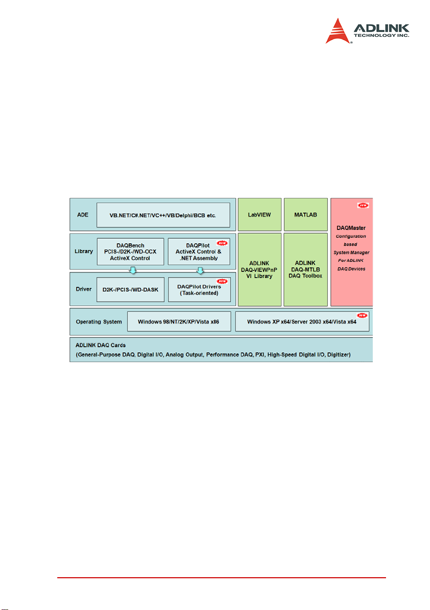
1.4 Software Support
ADLINK provides comprehensive software drivers and packages
to suit various user approach to building a system. Aside from programming libraries, such as DLLs, for most Windows-based systems, ADLINK also provides drivers for other application
environment such as LabVIEW
vides ActiveX component ware for measurement and SCADA/
HMI, and breakthrough proprietary software applications.
All software options are included in the ADLINK All-in-One CD.
®
and MA TLAB®. ADLINK also pro-
Figure 1-1: ADLINK Software Support Overview
Driver Support for Windows
DAQPilot
DAQPilot is a driver and SDK with a graphics-driven interface
for various application development environments. DAQPilot
comes as ADLINK's commitment to provide full support to its
comprehensive line of data acquisition products and is
designed for the novice to the most experienced programmer.
Introduction 5
Page 15
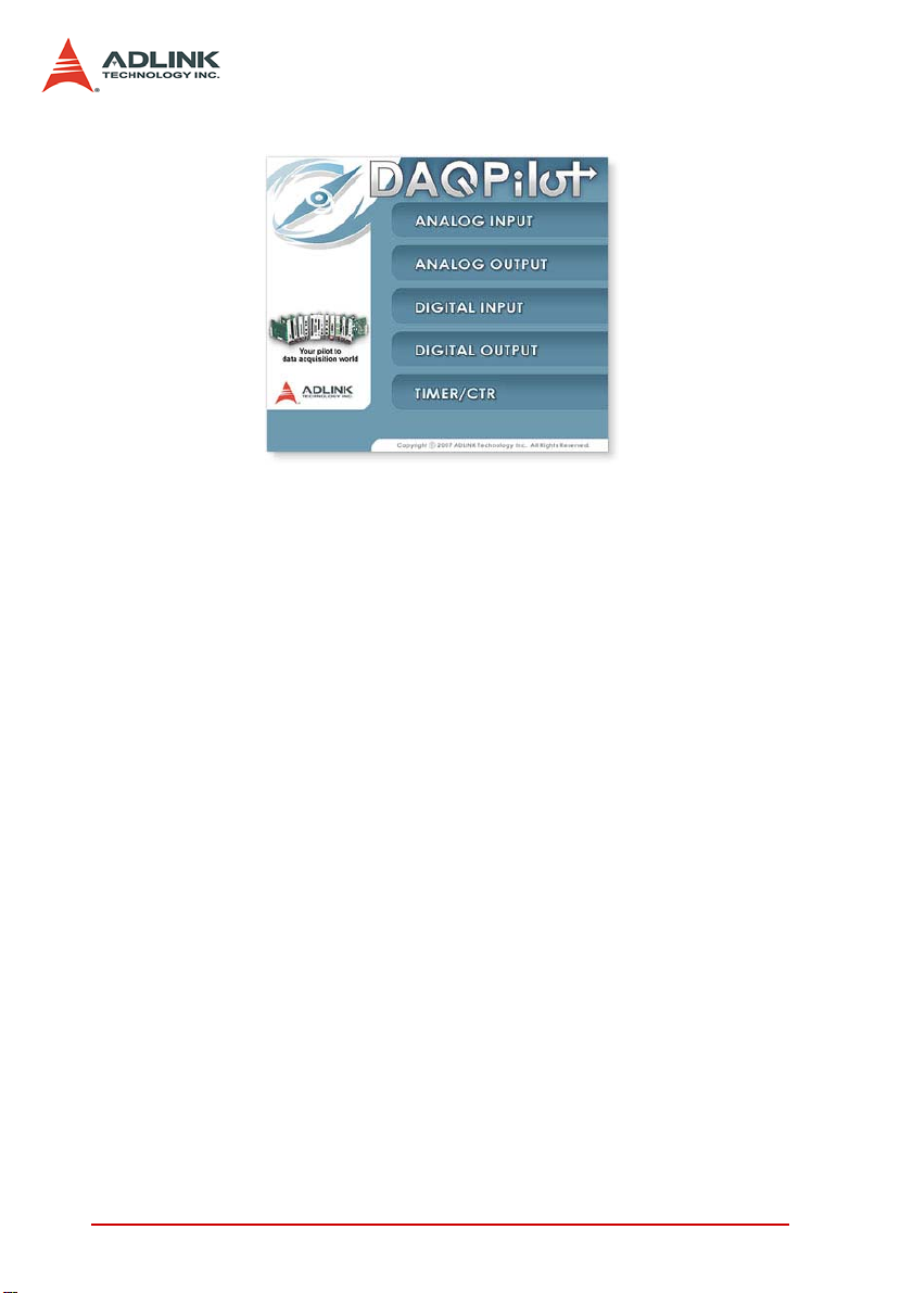
Figure 1-2: DAQPilot Main Interface
As a task-oriented DAQ driver, SDK and wizard for Windows
systems, DAQPilot helps you shorten the development time
while accelerating your learning curve for data acquisition programming.
You can download and install DAQPilot at
http://www.adlinktech.com/TM/DAQPilot.html
DAQMaster
The ADLINK DAQMaster is a smart device manager that
opens up access to ADLINK data acquisition an d test and measurement products. DAQMaster delivers all-in-one configurations and provides you with a full support matrix to properly and
conveniently configure ADLINK Test and Measurement products.
6Introduction
Page 16
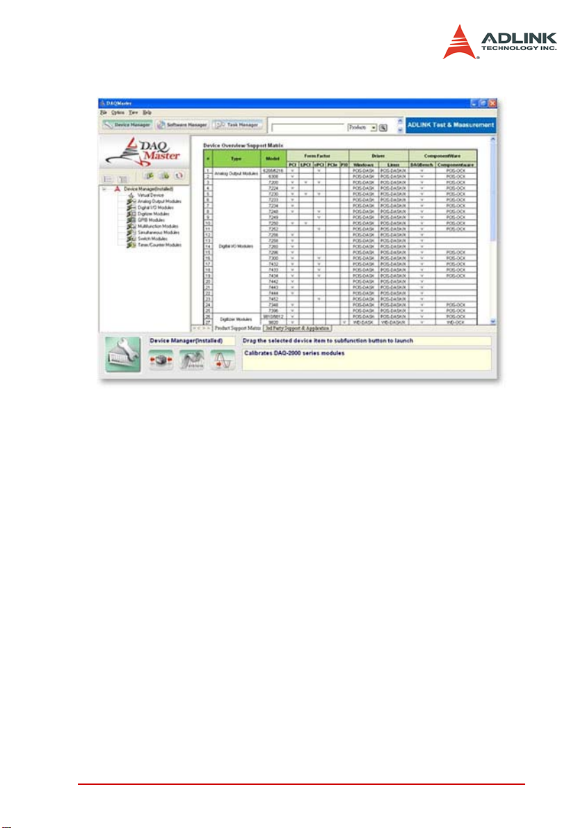
Figure 1-3: DAQMaster Device Manager
As a configuration-based device manager for ADLINK DAQ
cards, DAQMaster enables you to manage ADLINK devices
and interfaces, install and upgrade software applications, and
manage ADLINK DAQPilot tasks.
Introduction 7
Page 17

PCIS-DASK (Legacy Drivers and Support)
PCIS-DASK is composed of advanced 32-bit kernel drivers for
customized DAQ application development. PCIS-DASK
enables you to perform detailed operations and achieve superior performance and reliability from your data acquisition system. DASK kernel drivers now support the revolutionary
Windows Vista
®
OS.
Figure 1-4: Legacy Software Support Overview
NOTE ADLINK strongly recommends installing DAQPilot and
avoid using legacy DASK drivers. For current DASK driver users or those who do not have Internet access, we offer an installation CD. Contact your ADLINK distributor for
details.
8Introduction
Page 18

PCIS-DASK drivers prepare legacy Windows users for
Windows Vista and 64-bit editions of Windows. PCIS-DASK
comes with the following features:
Supports Windows Vista 32-bit or 64-bit editions
Supports AMD64 and Intel x86-64 architectures
Digitally-signed for Windows Vista 64-bit edition
Utilizes WOW64 subsystem to ensure that 32-bit
applications run normally on 64-bit editions of Windows XP,
Windows 2003 Server , and Windows Vista without
modification
For more information about Windows Vista support, visit
http://www.adlinktech.com/TM/VistaSupport.html, or view the
user’s guide included in the ADLINK All-in-one CD.
Introduction 9
Page 19

10 Introduction
Page 20

2 Installation
This chapter describes how to install the 7200 series. Package
contents and unpacking information are described. Because the
7200 series is a Plug and Play device, there are no jumper or DIP
switch settings for configuration. The interrupt number and I/O port
address are assigned by the system BIOS during system boot up.
2.1 Contents
In addition to this User's Manual, the package includes the following items:
PCI-7200 or PCIe-7200 Digital I/O & Counter Card
ACL-10437: 40-pin to 37-pin D-Sub cable
or
cPCI-7200 Digital I/O & Counter Module for 3U
ADLINK CD
Software Installation Guide
If any of these items is missing or damaged, contact the ADLINK
dealer. Save the shipping materials and carton to ship or store the
product in the future.
Installation 11
Page 21

2.2 Unpacking
The 7200 series contains sensitive electronic components that can
be easily damaged by static electricity.
The work area should have a grounded anti-static mat. The operator should be wearing an anti-static wristband, grounded at the
same point as the anti-static mat.
Inspect the card module carton for obvious damage. Shipping and
handling may cause damage to the module. Ensure there is no
shipping and handling damage on the module before proceeding.
After opening the card module carton, remove the system module
and place it only on a grounded anti-static surface compo nent side
up.
Again inspect the module for damage. Press down on all the socketed IC's to ensure that they are properly seated. Do this only with
the module place on a firm flat surface.
Note: DO NOT APPLY POWER TO THE CARD IF IT HAS BEEN
DAMAGED.
You are now ready to install your 7200 series card.
2.3 Device Installation for Windows Systems
Once Windows XP/2000 has started, the Plug and Play function of
Windows system will find the new NuDAQ cards. If this is the first
time to installing NuDAQ cards in this system, Windows will
require device information source. Please refer to the “Software
Installation Guide” for instructions on installing the device.
12 Installation
Page 22

2.4 PCI-7200/cPCI-7200/PCIe-7200 Layout
Figure 2-1: PCI-7200 Layout Diagram
Installation 13
Page 23

Figure 2-2: cPCI-7200 Layout Diagram
14 Installation
Page 24

2X-#4-40UNC
Figure 2-3: PCIe-7200 Layout Diagram
Installation 15
Page 25

2.5 Hardware Installation Outline
Hardware configuration
These PCI cards (or CompactPCI, PCI Express© cards) are
equipped with a Plug and Play PCI controller that requests
base addresses and interrupts according to PCI standard. The
system BIOS will install the system resource based on the PCI
cards’ configuration registers and system parameters (which
are set by system BIOS). Interrupt assignment and memory
usage (I/O port locations) of the PCI cards can be assigned by
system BIOS only. These system resource assignments are
done on a board-by-board basis. It is not recommended to
assign the system resource by any other meth o ds .
PCI slot selection
The PCI and Low-Profile PCI cards can be inserted to any PCI
slot without any configuration for system resource. CompactPCI peripheral slots are marke d with a circle on the backplane.
Please note that the PCI, CompactPCI, and PCI Express© system board must provide bus-mastering capability to operate
this board well.
Installation Procedure
1. Turn off the computer
2. Turn off all accessories (printer, modem, monitor, etc.)
connected to the computer
3. Remove the cover from your computer
4. Select a 32-bit PCI slot. PCI slots are shorter than the
ISA or EISA slots, and are usually white or ivory in color.
5. Before handling the PCI cards, discharge any static
buildup on your body by touching the metal case of the
computer. Hold the edge of the card and do not touch
the components.
6. Position the board into the PCI selected slot.
7. Secure the card in place at the rear panel of the system.
16 Installation
Page 26

2.6 Connector Pin Assignments
PCI/PCIe-7200 Pin Assignments
The PCI/PCIe-7200 comes equipped with one 37-pin D-Sub connector (CN2) located on the rear mounting plate and one 40-pin
female flat cable header connector (CN1). The CN2 is located on
the rear mounting plate; the CN1 is on front of the board. Refer
section 2.4 PCI-7200‘s layout.
CN2 is used for digital inputs (DI 0 to DI 15) and digital outputs
(DO 0 to DO 15) The reminding digital I/O channels DI 16 to DI 31
and DO 16 to DO 31 are on CN1. The pin assignment of CN1 and
CN2 is illustrated in the Figures 2-5 and 2.3.
Legend:
DO n Digital Output CH n
DI n Digital Input CH n
GND Ground
ACK ACK handshaking signal
REQ REQ handshaking signal
I_TRG Input signal to start DI data sampling
O_TRG Output signa l can be controlled by software
Installation 17
Page 27

Figure 2-4: CN1 Pin Assignments
21
20
2
34
56
78
910
11 12
13 14
15 16
17
19
22
23 24
25 26
27 28
37
18
29
35
3433
32
30
31
36
1
39 40
38
DI27
DI28
DI29
DI30
DI31
+5V
O_ACK
O_REQ
DI16
DI17
DI18
DI19
DI20
DI21
DI22
DI23
DI24
DI25
DI26
N/C
N/C
N/C
DO16
DO17
DO18
DO19
DO20
DO21
DO22
DO23
DO24
DO25
DO26
DO27
DO28
DO29
DO30
DO31
GND
O_TR1
21
20
2
34
56
78
910
11 12
13 14
15 16
17
19
22
23 24
25 26
27 28
37
18
29
35
3433
32
30
31
36
1
39 40
38
21
20
3
56
78
910
11 12
13 14
15 16
17
19
22
23 24
25 26
27 28
37
18
29
35
3433
32
30
31
36
1
39
38
DI27
DI28
DI29
DI30
DI31
+5V
O_ACK
O_REQ
DI16
DI17
DI18
DI19
DI20
DI21
DI22
DI23
DI24
DI25
DI26
N/C
N/C
N/C
DO16
DO17
DO18
DO19
DO20
DO21
DO22
DO23
DO24
DO25
DO26
DO27
DO28
DO29
DO30
DO31
GND
O_TR1
1
2
3
4
5
6
10
11
12
13
14
15
7
8
9
16
17
18
19
20
21
22
23
24
25
26
27
28
30
31
32
33
29
35
36
37
34
DI 1
DI 2
DI 3
DI 4
DI 5
DI 6
DI 7
DI 8
DI10
DO10
DO11
DO12
DO13
DO14
DO15
DI 9
GND
I_TRG
DO0
DO1
DO2
DO3
DO4
DO5
DO6
DO7
DO8
DO9
DI 0
DI11
DI12
DI13
DI14
DI15
+5V
I_ACK
I_REQ
18 Installation
Figure 2-5: CN2 Pin Assignments
Page 28

cPCI-7200 Pin Assignments
Figure 2-6: CN Pin Assignments
Installation 19
Page 29

2.7 8254 for Timer Pacer Generation
Timer 0
Timer 1
Timer 2
CLK0
GATE0
OUT0
CLK1
GATE1
CLK2
GATE2
OUT1
OUT2
8254 Timer/C ounter
Digital Input Timer Pacer
Digital Output Timer Pacer
4MHz Clock
“H”
“H”
“H”
Figure 2-7: 8254 configuration
The internal timer/counter 8254 on the 7200 series is configured
as the above diagram (Figure 2.7). Users can use it to generate
the timer pacer for both digital input and digital output triggers.
The digital input timer pacer is from OUT0 (Timer 0), and the digital output timer pacer is from OUT1 (Timer 1). Besides, Timer 0
and Timer 2 can be cascaded together to generate more timer
pacer frequencies for digital input. Also, Timer 2 can be cascaded
with Timer 1 for digital output.
pacer rate = 4MHz / ( C0 * C2)
if Timer 0 & Timer 2 are cascaded
pacer rate = 4MHz / C0
if timer 0 & Timer 2 are not cascaded
The maximum pacer signal rate of input and output are 4MHz/2 =
2MHz. The minimum signal rate is 4MHz/65535/65535.
For example, to get a pacer rate of 2.5kHz, set C0 = 40 and C2 =
40. That is 2.5kHz = 4MHz / (40 x 40)
20 Installation
Page 30

2.8 Onboard Pull-ups and Terminations on the Digital Inputs
The PCI-7200, cPCI-7200 and PCIe-7200 have 32 digital input
channels. Onboard terminations for digital input circuits may be
needed for some applications. Schottky terminations can minimize
undershoot/overshoot disturbances caused by reflection noise on
high-speed bus lines. Table 2.1 lists the pull-ups and termination
status of PCI-7200, cPCI-7200, and PCIe-7200. Figure 2.8 is the
illustration of the pull-up resistor and terminations on-board.
Pull-up resistor Terminations
PCI-7200 /
PCIe-7200
cPCI-7200 None Schottky diode clamped to ground & power
None None
Table 2-1: 7200 Series Termination
Figure 2-8: Digital Input Pull-up Resistor and Termination Circu it Dia gram
Installation 21
Page 31

22 Installation
Page 32

3 Register Format
3.1 I/O Registers Format
The PCI/PCIe-7200 occupies eight consecutive 32-bit I/O
addresses in the PC I/O address space. The cPCI-7200 occupies
nine consecutive 32-bit I/O addresses. Table 4-1 shows the I/O
Map.
Address Read Write
Base + 0 Counter 0 Counter 0
Base + 4 Counter 1 Counter 1
Base + 8 Counter 2 Counter 2
Base + C --- CLK Control CW0
Base + 10 Digital Input Reg. --Base + 14 Digital Output (Read-back) Digital Output Reg.
Base + 18 DIO Status & Control DIO Status &Control
Base + 1C INT Status & Control INT Status & Control
Base + 20 (cPCI-7200 only) AUXDIO Reg. AUXDO Reg.
Note: (1) I/O port is 32-bits wide
(2) 8-bit or 16-bit I/O access is not allowed
3.2 Digital Input Register (BASE + 10)
32 digital input channels can be read from this register
Address: BASE + 10
Attribute: READ Only
Data Format:
Byte 7 6 5 4 3 2 1 0
Base +10 DI7 DI6 DI5 DI4 DI3 DI2 DI1 DI0
Base +11 DI15 DI14 DI13 DI12 DI11 DI10 DI9 DI8
Base +12 DI23 DI22 DI21 DI20 DI19 DI18 DI17 DI16
Base +13 DI31 DI30 DI29 DI28 DI27 DI26 DI25 DI24
Register Format 23
Page 33

3.3 Digital Output Register (BASE + 14)
32 digital output channels can be written and read to/from this register
Address: BASE + 14
Attribute: READ/WRITE
Data Format:
Byte 7 6 5 4 3 2 1 0
Base +14 DO7 DO6 DO5 DO4 DO3 DO2 DO1 DO0
Base +15 DO15 DO14 DO13 DO12 DO11 DO10 DO9 DO8
Base +16 DO23 DO22 DO21 DO20 DO19 DO18 DO17 DO16
Base +17 DO31 DO30 DO29 DO28 DO27 DO26 DO25 DO24
The digital output status can be read back through the same location (BASE + 14)
3.4 DIO Status & Control Register (BASE + 18)
The data transfer mode of digital input is controlled and status is
checked through this register.
Address: BASE + 18
Attribute: READ/WRITE
Data Format:
Byte 7 6 5 4 3 2 1 0
Base +18 O_ACK DIN_EN I_TRG TRGPL I_FIFO I_TIME0 I_REQ I_ACK
Base +19 ---- I_OVER ---- ---- O_TRG O_FIFO O_TIME1 O_REQ
Base +20 ---- ---- ---- ---- ---- ---- ---- O_UND
Base +21 ---- ---- ---- ---- ---- ---- ---- ----
Digital Input Mode Setting:
I_ACK: Input ACK Enable
1: Input ACK is enabled (input ACK will be asserted after input data is read by CPU or written to input FIFO)
0: Input ACK is disabled
24 Register Format
Page 34

I_REQ: Input REQ Strobe Enabled
1: Use I_REQ edge to latch input data
0: I_REQ is disabled
I_TIME0: Input Timer 0 Enable
1: Input is sampled by falling edge of Counter 0 output
(COUT0)
0: Input Timer 0 is disabled
I_FIFO: Input FIFO Enable Mode
1: Input FIFO is enabled (input data is saved to input FIFO)
0: Input FIFO is disabled
TRGPOL: Input Trigger Polarity
1: I_TRG is Rising Edge Active
0: I_TRG is Falling Edge Active
I_TRG: External Trigger Enable
1: Wait until I_TRG signal is active, digital input sampling will
begin after a rising or falling edge of I_TRG
0: Start input sampling immediately (if input control register
is set)
DIN_EN: Digital Input Enable
1: Digital Input Enable
0: Digital Input Disabled, when this bit is set as 0, all digital
input operation will be stopped
Digital Output Mode Setting:
O_ACK: Output ACK Enable
1: Output ACK is enabled; the output circuit will wait for
O_ACK after O_REQ strobe is asserted
0: Output ACK is disabled
O_REQ: Output REQ Enable
1: Output REQ is enabled; an O_REQ strobe will be generated after output data is ready
0: Output REQ is disabled
O_TIME1: Output Timer 1 Enable
1: Output Timer 1 is enabled; output data is moved from out-
Register Format 25
Page 35

put FIFO to DO registers when output of Counter1 goes low
0: Output Counter 1 is disabled
O_FIFO: Output FIFO Enable
1: Output FIFO is enabled (output data is moved from output
FIFO)
0: Output FIFO is disabled
O_TRG: Digital Output Trigger Signal
This bit is used to control the O_TRG output of PCI-7200; the
signal is on CN1 pin 36 of PCI-7200, CN1 pin 26 of cPCI7200, CN2 pin 34 of LPCI 7200S when
1: O_TRG 1 goes High (1)
0: O_TRG 1 goes Low (0)
Digital I/O FIFO Status:
I_OVR: Input data overrun
1: Digital Input FIFO is full (overrun) during input data transfer
0: No input data overrun occurred
Input data overrun occurred, the I_OVR bit is set when input
FIFO is full and there is new input data coming in. This bit
can be cleared by writing “1” to it.
O_UND: Output data FIFO is underrun
1: Output FIFO is empty during output data transfer
0: No output data underrun occurred
Output data underrun, the O_UND bit is set when output
FIFO is empty and the output request for new da ta , this bit
can be cleared by writing “1” to it.
26 Register Format
Page 36

3.5 Interrupt Status & Control Register (BASE + 1C)
The interrupt mode/status is set/checked through this register.
Address: BASE + 1C
Attribute: READ/WRITE
Data Format:
Byte 7 6 5 4 3 2 1 0
Base +1C SI_TO SI_REQ SO_ACK T2_EN T1_EN T0_EN I I_REQ IO_ACK
Base +1D FIFOFF FIFOEF FIFORST REQ_NEG T1_T2 T0_T2 SI_T2 SI_T1
Base +1E ---- ---- ---- ---- ---- ---- ---- ---Base +1F ---- ---- ---- ---- ---- ---- ---- ----
Interrupt Control:
With the 7200 series, interrupts can be triggered by many
signal sources such as O_ACK, I_REQ, timer 0, timer 1, and
timer 2. The following bits control the interrupt source:
IO_ACK: Interrupt is triggered by O_ACK signal.
1: O_ACK interrupt is enabled
0: O_ACK interrupt is disabled
II_REQ: Interrupt is triggered by I_REQ signal.
1: I_REQ interrupt is enabled
0: I_REQ interrupt is disabled
T0_EN: Interrupt is triggered by timer 0 output.
1: Timer 0 interrupt is enabled
0: Timer 0 interrupt is disabled
T1_EN: Interrupt is triggered by timer 1 output.
1: Timer 1 interrupt is enabled
0: Timer 1 interrupt is disabled
T2_EN: Interrupt is triggered by timer 2 output.
1: Timer 2 interrupt is enabled
0: Timer 2 interrupt is disabled
Interrupt Status:
Register Format 27
Page 37

The following bits are used to check interrupt stat us:
SO_ACK: Status of O_ACK interrupt
1: O_ACK Interrupt occurred
0: No O_ACK interrupt
SI_REQ: Status of I_REQ interrupt
1: I_REQ Interrupt occurred
0: No I_REQ Interrupt
SI_T0: Status of timer 0 interrupt
1: OUT0 (output of timer 0) Interrupt occurred
0: No timer 0 Interrupt
SI_T1: Status of timer 1 interrupt
1: OUT1 (output of timer 1) Interrupt occurred
0: No timer 1 Interrupt
SI_T2: Status of timer 2 interrupt
1: OUT2 (output of timer 2) interrupt occurred
0: No timer 2 Interrupt
Note: Writing “1” to the corresponding bit of the register can clear
all interrupt statuses. In order to make the interrupt work
properly, the interrupt service routine has to clear all the interrupt status before end of the ISR.
Timer Configuration Control:
The 8254 timer on the 7200 series can be configured as either timer 0 cascaded with timer 2 or timer 1 cascaded with
timer 2. These configurations are controlled by the following
bits:
T0_T2: Timer 0 is cascaded with timer 2
1: Timer 0 and timer 2 are cascaded together; output of timer
2 connects to the clock input of timer 0.
0: Not cascaded, the 4MHz clock is connected to the timer 0
clock input.
T1_T2: Timer 1 is cascaded with timer 2
1: Timer 1 and timer 2 are cascaded together; output of timer
2 connects to the clock input of timer 1.
28 Register Format
Page 38

0: Not cascaded, the 4MHz clock is connected to the timer 1
clock input.
I_R EQ Polarity Selection:
When the input sampling is controlled by the I_REQ signal
only, the I_REQ can be programmed to be rising edge active
or falling edge active.
REQ_NEG: I_REQ trigger polarity
1: latch input data on falling edge of I_REQ
0: latch input data on rising edge of I_REQ
FIFO Control and Status (cPCI-7200 only):
The cPCI-7200 has an extra 2k samples digital input FIFO.
The FIFO can be cleared and monitored by the following bits:
FIFORST (Write only): Clear the on-board DI FIFO
1: Write 1 to clear the data of the FIFO.
0: No operation.
FIFOEF (Read only): Empty flag of the DI FIFO
1: DI FIFO is empty.
0: DI FIFO is not empty.
FIFOFF (Read only): Full flag of the DI FIFO
1: DI FIFO is full.
0: DI FIFO is not full.
Note: The cPCI-7200 has two cascaded DI FIFOs. One is located
in the PCI controller chip, the other one is on the PCI-7200
board. The above bits only control the onboard FIFO. In order to control the on-chip FIFO, please refer to the AMCC5933 data book.
Register Format 29
Page 39

3.6 8254 Timer Registers (BASE + 0)
The 8254 timer/counter IC occupies four I/O address. Users can
refer to Tundra's or Intel's data sheet for a full description of the
8254 features. Download the 8254 data sheet from the following
web site:
http://support.intel.com/support/controllers/peripheral/231164.htm
or
http://www.tundra.com (for Tundra’s 82C54 datasheet).
Address Read Write
Base + 0 Counter 0 Counter 0
Base + 4 Counter 1 Counter 1
Base + 8 Counter 2 Counter 2
Base + C --- CLK Control CW0
30 Register Format
Page 40

4 Operation Theory
In the 7200 series, there are four data transfer modes can be used
for digital I/O access and control, these modes are:
1. Direct Program Control: the digital inputs and outputs
can be read/written and controlled by its corresponding I/
O port address directly.
2. Internal Timer Pacer Mode: the digital input and output
operations are paced by an internal timer pacer and are
transferred by bus mastering DMA.
3. External Clock Mode: the digital input operation is
clocked by external I_REQ strobe and transferred by bus
mastering DMA.
4. Handshaking: through REQ and ACK signals, the digital
I/O can have simple handshaking data transf er s.
4.1 Direct Program Control
Digital I/O operations can be controlled by I/O port BASE+10 for
digital input and BASE+14 for digital output.
The I/O port address BASE is assigned by system BIOS, please
refer to Section 5 for a more detailed description.
The digital OUT operation is:
outport (BASE+14, 0xAAAAAAAA) // (A : 0 to F)
The digital IN operation is:
value = inport (BASE+10) // The input status
is save in the // value variable
Operation Theory 31
Page 41

4.2 Timer Pacer Mode
Timer 0
Timer 1
Timer 2
CLK0
GATE0
OUT0
CLK1
GATE1
CLK2
GATE2
OUT1
OUT2
8254 Timer/Counter
Digital Input Timer Pacer
Digital Output Timer Pacer
4MHz Clock
“H”
“H”
“H”
The digital I/O access control is clocked by timer pacer, which is
generated by an interval programming timer/counter chip (8254).
There are three timers on the 8254. Timer 0 is used to generate
timer pacer for digital input and timer 1 is used for digital output.
The configuration is illustrated as below.
The operation sequences are:
1. Define the frequency (timer pacer rate)
2. The digital input data are saved in FIFO after a timer
pacer pulse is generated. The sampling is controlled by
timer pacer.
3. The data saved in FIFO will be transferred to main memory of the computer system directly and automatically.
This is controlled by bus mastering DMA control, this
function is supported by PCI controller chip.
The operation flow is show as following:
32 Operation Theory
Page 42

4.3 External Clock Mode
To Digital Input Trigger
Latch Digital
Input Data
Digital Input FIFO
Bus mastering
DMA data Transfer
PC's Main Memory
1
2
3
Pin 19 of CN2
The digital input is clocked by external strobe, which is from Pin 19
(I_REQ) of CN2 (PCI/PCIe-7200) or Pin 24 of CN1 (cPCI-7200).
The operation sequence is very similar to the Timer Pacer Trigger.
The only difference is the clock source.
1. The external input strobe is generated from outside
device, and goes through the Pin 19 (I_REQ) of CN2 to
latch the digital input.
2. The digital input data is saved in FIFO after an I/O strobe
signal is coming in.
3. The data saved in input FIFO will be transferred to main
memory on your computer system directly. This is controlled by bus mastering DMA control, this function is
supported by PCI.
Operation Theory 33
Page 43
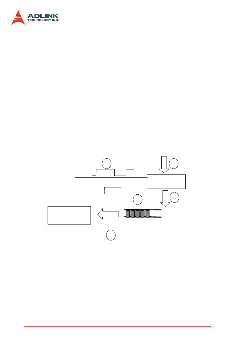
4.4 Handshaking
Latch Digital Input
or Digital Output
Digital Input FIFO Bus mastering
DMA data Transfer
PC's Main Memory
2
4
3
1
Digital Input DATA
5
IN_REQ
IN_ACK
The 7200 series also supports a handshaking digital I/O transfer
mode. That is, after input data is ready, an I_REQ is sent from an
external device, and I_ACK will go high to acknowledge the data
already accessed.
I_REQ & I_ACK for Digital Input
1. Digital Input Data is ready.
2. An I_REQ signal is generated for digital input operation.
3. Digital input data is saved to FIFO.
4. An I_ACK signal is generated and sent to an outside
device.
5. If the FIFO is not empty and PCI bus is not occupied, the
data will be transferred to main memory.
34 Operation Theory
Page 44

O_REQ & O_ACK for Digital Output
Move Data to
Digital Output FIFO
Bus mastering
DMA data Transfer
PC's Main
Memory
2
4
3
1
Digital Output DATA
5
Digital Output
O_REQ
O_ACK
1. Digital Output Data is moved from PC memory to FIFO
of the 7200 series by using DMA data mastering data
transfer.
2. Move output data from FIFO to digital output circuit.
3. Output data is ready.
4. An O_REQ signal is generated and sent to outside
device.
5. After an O_ACK is captured, steps 2-5 will be repeated.
** If the FIFO is not full, the output data is moved form PC‘s
main memory to FIFO automatically.
Operation Theory 35
Page 45

4.5 Timing Characteristic
IN_ I_REQ
t
l
t
cyc
t
h
t
s
valid data
D10~DI31
t
n
valid data
t
s
valid data
D10~DI31
t
n
valid data
IN_R I_REQ
t
cyc
t
l
t
h
1. I_REQ as input data strobe (Rising Edge Active)
th 60ns tI 60ns tCYC 5 PCI CLK Cycle
ts 2ns tn 30ns
2. I_REQ as input data strobe (Falling Edge Active)
th
60ns tI 60ns tCYC 5 PCI CLK Cycle
ts 2ns tn 30ns
36 Operation Theory
Page 46

3. I_REQ & I_ACK Handshaking
valid data
D10~DI31
valid data
t1
t2
t5
t4t3
IN I_REQ
IN I_ACK
t1 0ns t5 60ns t3 2 PCI CLK Cycle
t2 0ns t4 1 PCI CLK Cycle
Note: I_REQ must be asserted until I_ACK asserts, I_ACK will be
asserted until I_REQ de-asserts.
4. O_REQ as output data strobe
ts
19ns th 2 PCI CLK Cycles Tcyc 500ns
5. O_REQ & O_ACK Handshaking
Note: O_ACK must be de-asserted before O_REQ asserts,
O_ACK can be asserted any time after O_REQ asserts,
O_REQ will be reasserted after O_ACK is asserted.
Operation Theory 37
Page 47

38 Operation Theory
Page 48

5 Double Buffer Mode Principle
Incoming DMA
input data
Circular Buffer
Transfer Buffer
a
b
c
d
> > >
> > >> >
Empty Buffer Untransferred Data Transferred Data
> >
The data buffer for a double-buffered DMA DI operation is logically
a circular buffer divided into two equal halves. The double buf fered
DI begins when the device starts writing data into the first half of
the circular buffer (Figure 6-1a). After device begins writing to the
second half of the circular buffer, users can copy the data from the
first half into the transfer buffer (Figure 6-1b). Users can now process the data in the transfer buffer according to application needs.
After the board has filled the second half of the circular buffer, the
board returns to the first half buffer and overwrites the old data.
Users can now copy the second half of the circular buffer to the
transfer buffer (Figure 6-1c). The data in the transfer buffer is
again available for process. The process can be repeated endlessly to provide a continuous stream of data to applications (Figure 6-1d).
Figure 5-1: Double Buffer Mode
Double Buffer Mode Principle 39
Page 49

40 Double Buffer Mode Principle
Page 50

6 Limitations
The 12 MB/sec data transfer rate can only be possibly achieved in
systems where the 7200 series card is the only device using the
bus, but the speed cannot be guaranteed due to the limited FIFO
depth.
The 7200 series supports three input clock modes, internal clock,
external clock, and handshaking modes. The first two modes cannot guarantee the input data integrity in high-speed data rate
because of the limited FIFO depth and PCI-bus late ncy variation.
The handshaking mode is the only mode that data integrity can be
guaranteed. During handshaking, expect 12 MB/sec data rate on
average, but the speed is not guaranteed.
The guaranteed data rate with internal clock or external clock
mode is 1 MB/sec on systems where 7200 series card is the only
device using the bus.
The largest transfer size (in bytes) 7200 series can perform is 64
MB.
Limitations 41
Page 51

42 Limitations
 Loading...