

Page 1

PCI-8144
4-Axis Stepper
Motion Control Card
User’s Manual
Manual Rev. 2.01
Revision Date: September 2, 2008
Part No: 50-11144-1010
Advance Technologies; Automate the World.
Page 2

Copyright 2008 ADLINK TECHNOLOGY INC.
All Rights Reserved.
The information in this document is subject to change without prior
notice in order to improve reliability , design, and function and does
not represent a commitment on the part of the manufacturer.
In no event will the manufacturer be liable for direct, indirect, special, incidental, or consequential damages arising out of the use or
inability to use the product or documentation, even if advised of
the possibility of such damages.
This document contains proprietary information protected by copyright. All rights are reserved. No part of this manual may be reproduced by any mechanical, elec tronic, or other means in a ny form
without prior written permission of the manufacturer.
Trademarks
NuDAQ, NuIPC, DAQBench are registered trademarks of ADLINK
Technology Inc.
Product names mentioned herein are used for identification pur-
poses only and may be trademarks and/or registered trademarks
of their respective companies.
Page 3
Getting Service from ADLINK
Customer Satisfaction is top priority for ADLINK Technology Inc.
Please contact us should you require any service or assistance.
ADLINK TECHNOLOGY INC.
Web Site: http://www.adlinktech.com
Sales & Service: Service@adlinktech.com
TEL: +886-2-82265877
FAX: +886-2-82265717
Address: 9F, No. 166, Jian Yi Road, Chungho City,
Taipei, 235 Taiwan
Please email or FAX this completed service form for prompt and
satisfactory service.
Company Information
Company/Organization
Contact Person
E-mail Address
Address
Country
TEL FAX:
Web Site
Product Information
Product Model
OS:
Environment
M/B: CPU:
Chipset: BIOS:
Please give a detailed description of the problem(s):
Page 4

Page 5

Table of Contents
Table of Contents..................................................................... i
List of Tables........................................................................... v
List of Figures........................................................................ vi
1 Introduction ........................................................................ 1
1.1 Features............................................................................... 5
1.2 Specifications....................................................................... 6
1.3 Supported Software............................................................. 7
Programming Library ........................................ ... ...........7
MotionCreatorPro ........................................................... 7
2 Installation .......................................................................... 9
2.1 Package Contents ............................................................... 9
2.2 PCI-8144 Outline Drawing................................................. 10
2.3 PCI-8144 Hardware Installation......................................... 11
Hardware configuration .................................................11
PCI slot selection ................. ... ... .... ... ... ... ......................11
Installation Procedures .................................................11
Troubleshooting: ............................... ............................11
2.4 Software Driver Installation................................................ 13
2.5 SW1 Card Index Selection................................................. 13
2.6 J1-J8 Pulse Output Type: Differential / Open Collector..... 14
2.7 JP2 Direct Control to Stepper ........................................... 14
2.8 CN1 Pin Assignments: Main connector ............................. 15
3 Signal Connections.......................................................... 17
3.1 Pulse Output Signals CW and CCW.................................. 18
3.2 Origin Signal ORG............................................................. 21
3.3 Slow Down input signal........................ ... ... ... ... .... ... ... ... .... . 22
3.4 End-Limit Signals PEL and MEL........................................ 23
3.5 Simultaneously Start/Stop Signals STA and STP.............. 24
3.6 Termination Board............................................................. 25
3.7 General Purpose DIO........................................................ 25
Isolated Input channels .................................................26
Isolated Output channels .............................................. 26
Example of input connection .........................................26
Table of Contents i
Page 6

Example of output connection ......................................27
3.8 JP2 pin define for stepping singal (Optional)..................... 27
4 Operation Theory.............................................................. 29
4.1 Classifications of Motion Controller.................................... 29
Voltage motion control interface ................................... 29
Pulse motion control interface ......................................30
Network motion control interface .................................. 30
Software real-time motion control kernel ..................... .31
DSP motion control kernel ............................................31
ASIC motion control kernel ...........................................31
Compare Table of all motion control types ...................32
PCI-8144 motion controller type ...................................32
4.2 Motion Control Modes........................................................ 33
Coordinate system ........................................................33
Absolute and relative position move .............................34
Trapezoidal speed profile .............................................35
S-curve and Bell-curve speed profile .................. .......... 36
Velocity mode ...............................................................38
One axis position mode ................................................39
Home Return Mode ......................................................40
Synchronous Start Function .........................................41
Auto Home Move Mode ................................................42
4.3 The motor driver interface.................................................. 44
Pulse Command Output Interface ................................44
4.4 Mechanical switch interface............................................... 46
Original or home signal .................................................46
End-Limit switch signal .................................................46
Slow down switch ..................................... ... ... .... ... ... ... .46
4.5 The Counters..................................................................... 47
Preset Command position counter ...............................47
4.6 Interrupt Control.......... .... ... ... ... .......................................... 47
4.7 Multiple Card Operation..................................................... 50
5 MotionCreatorPro ............................................................. 51
5.1 Run MotionCreatorPro....................................................... 51
5.2 About MotionCreatorPro....................................... .... ... ... ... 52
5.3 MotionCreatorPro Form Introducing .................................. 53
Main Menu ...................................................... .... ... ... ... .53
Select Menu ................................. ... .... ... ... ... ... .... ... ... ....54
ii Table of Contents
Page 7

Card Information Menu .................................. ............... 55
Configuration Menu .......... ... ... ... .... ... ... ... ... .... ... ... ... .... .. 56
Single Axis Operation Menu .........................................59
Four-Axis Operation Menu ............................................ 63
Help Menu ....................................................................65
6 Function Library............................................................... 67
6.1 List of Functions................................................................. 68
6.2 C/C++ Programming Library.............................................. 71
6.3 System and Initialization.................................................... 72
_8144_initial ................................................................. 72
_8144_close ................................................................. 74
_8144_get_version ....................................................... 75
_8144_set_security_key ................................... ............ 76
_8144_check_security_key ..........................................78
_8144_reset_security_key ................................... .........80
_8144_config_from_file ................................................ 82
6.4 Motion Interface I/O ........................................................... 83
_8144_set_limit_logic ................................................... 83
_8144_get_limit_logic ....................................... ............ 85
_8144_get_mio_status .................................................87
_8144_set_mio_sensitivity ............................. ... ... ... .... .. 89
_8144_set_pls_outmode .............................................. 91
_8144_set_pls_outmode2 ............................................ 93
6.5 Motion................................................................................ 94
_8144_tv_move ............................................................ 94
_8144_sv_move ........................................................... 96
_8144_start_tr_move ..................................... ............... 98
_8144_start_sr_move .................................................101
_8144_enable_get_command .................................... 104
_8144_get_command ....................................... .......... 105
_8144_set_command ................................................. 106
_8144_set_external_start ........................................... 107
_8144_emg_stop ........................................................109
_8144_dec_stop ......................................................... 111
_8144_speed_up .................................... .................... 113
_8144_slow_down ............................... ....................... 114
_8144_enable_org_stop ...................................... ....... 116
_8144_enable_sd_signal ........................................ ....118
_8144_home_move .......................................... .......... 120
Table of Contents iii
Page 8

_8144_home_status ................................................... 122
6.6 Motion status.................................................................... 125
_8144_motion_done ................................................... 125
_8144_motion_status .................................................127
6.7 Interrupt ................ ... ... .... ... ... .......................................... . 129
_8144_set_motion_interrupt_factor ............................ 129
_8144_wait_single_motion_interrupt ..........................131
_8144_set_gpio_interrupt_factor ................................ 134
_8144_wait_single_gpio_interrupt ..............................136
_8144_wait_multiple_gpio_interrupt ........................... 138
6.8 General purpose input/output ...................................... ... . 141
_8144_get_gpio_input ................................................ 141
_8144_get_gpio_input_channel ..................................142
_8144_set_gpio_output .............................................. 143
_8144_set_gpio_output_channel ................................144
_8144_get_gpio_output .............................................. 145
_8144_get_gpio_output_channel ............................... 146
6.9 Speed profile calculation.................................................. 147
_8144_get_tv_move_profile .......................................147
_8144_get_sv_move_profile ..................................... ..149
_8144_get_start_tr_move_profile ............................... 151
_8144_get_start_sr_move_profile .............................. 153
7 Function Return Code.................................................... 155
iv Table of Contents
Page 9

List of Tables
Table 2-1: SW1 Card Index ..................................................... 13
Table 2-2: JP2 Direct Control to Stepper ................................. 14
Table 2-3: CN1 Pin Assignments ............................................. 15
Table 6-1: Data type definitions .............................................. 71
List of Tables v
Page 10

List of Figures
Figure 1-1: PCI-8144 Block Diagram ........................................... 2
Figure 1-2: Flow chart for building an application ........................ 4
Figure 2-1: PCB Layout of the PCI-8144 ................................... 10
vi List of Figures
Page 11

1 Introduction
The PCI-8144 is a cost-effective 4-axis motion controller card with
a PCI interface that can generate a pulse train up to 2.4MHz to
control a stepper motor. As a motion controller, it provides nonsymmetric acceleration and deceleration speed profile settings, Tcurve and S-surve speed profile control, and simultaneously start/
stop. Changing speed on the fly is also available with a single axis
operation.
Multiple PCI-8144 cards can be installed in one system. The onboard switch can be used to the set a specific index for each board
in order to manage multiple cards.
Figure 1 shows the functional block diagram of the PCI-8144 card.
All functions and computations are performed internally by the
ASIC, thus limiting the impact on the PC’s CPU.
Introduction 1
Page 12
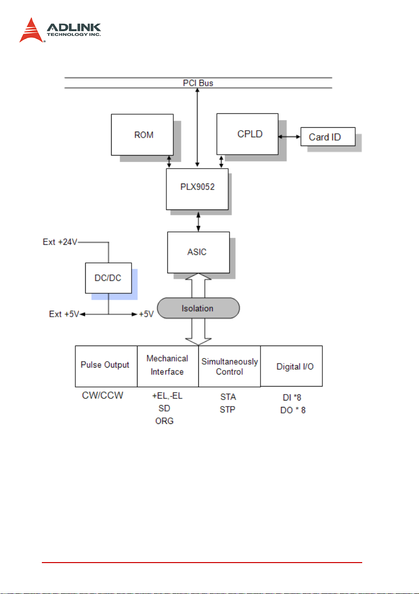
Figure 1-1: PCI-8144 Block Diagram
2Introduction
Page 13

MotionCreatorPro is a Windows-based application development
software package included with the PCI-8144 and is useful for
debugging a motion control system during the design phase of a
project. An on-screen display lists information of all installed axes
and I/O signal status of the PCI-8144.
Windows programming libraries are also included for C++ and
Visual Basic. Sample programs are provided to illustrate the operations of the functions.
Introduction 3
Page 14
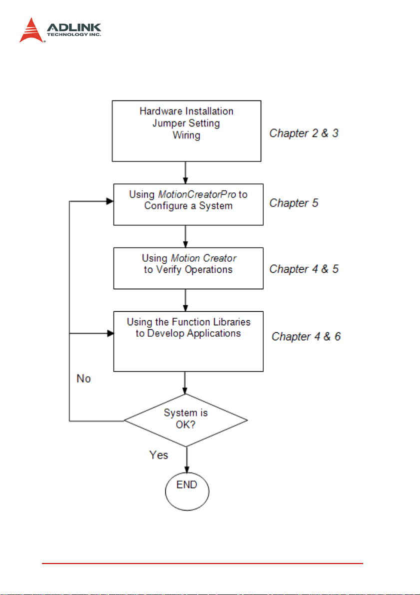
Figure 1-2 illustrates a flow chart of the recommended process in
using this manual in developing an application. Refer to the
related chapters for details of each step.
Figure 1-2: Flow chart for building an application
4Introduction
Page 15

1.1 Features
The following list summarizes the main features of the PCI-8144
motion control system.
X 32-bit PCI bus Plug and Play
X 4 pulse train channel for stepping motors
X Maximum output frequency: up to 2.4MPPS
X Pulse output options: CW/CCW
X Programmable acceleration and deceleration time for all
modes
X Trapezoidal and S-curve velocity profiles for all modes
X Change speed on the fly
X Home return modes with ORG & SD signal
X Hardware backlash compensator and vibration suppression
X Card index setting by switch
X All digital input and output signals are 2500Vrms isolated
X Programmable interrupt sources
X Simultaneous start/stop
X Software supports a maximum of up to 12 PCI-8144 cards
operation in one system
X Includes MotionCreatorPro, a Microsoft Windows-based
application development software
X PCI-8144 libraries and utilities for Windows 2000/XP.
Introduction 5
Page 16

1.2 Specifications
Applicable Motors
Z Stepping motors
Z Excitation sequencing output for 2-phase stepping motor
with JP2 connector
Performance
Z Number of controllable axes: 4
Z Maximum pulse output frequency: 2.4MPPS, trapezoi-
dal, or S-Curve speed profile
Z Internal reference clock: 4.9MHz
Z Position pulse setting range (28-bit): -134,217,728 to
+134,217,728
I/O Signales
Z Input/Output signals for each axis
Z All I/O signal are optically isolated with 2500Vrms isola-
tion voltage
Z Command pulse output pins: CW and CCW
Z Mechanical limit/switch signal input pins: ±EL, PSD/
MSD, and ORG
Z Digital input/output: DIN & DOUT
Z Simultaneous Start/Stop signal: STA and STP
General Specifications
Z Connectors: 68-pin SCSI-type connector
Z Operating Temperature: 0°C - 50°C
Z Storage Temperature: -20°C - 80°C
Z Humidity: 5 - 85%, non-condensing
Power Consumption
Z Slot power supply (input): +5V DC ±5%, 900mA max
Z External power supply (input): +24V
max
Z External power supply (output): +5V
max
±5%, 500mA
DC
±5%, 500mA,
DC
6Introduction
Page 17

PCI-8144 Dimensions
Z 159mm(L) X 126 mm(W)
1.3 Supported Software
1.3.1 Programming Library
Windows 2000/XP DLLs are provided for the PCI-8144. These
function libraries are shipped with the board.
1.3.2 MotionCreatorPro
This Windows-based utility is used to setup cards, motors, and
systems. It can also aid in debugging hardware and sof tware problems. It allows for the setting of I/O logic parameters to be loaded
in custom program. This product is also bundled with the card.
Refer to Chapter 5 for more details.
Introduction 7
Page 18

8Introduction
Page 19

2 Installation
This chapter describes how to install PCI-8144. Please follow
these steps below:
X Check what you have (section 2.1)
X Check the PCB (section 2.2)
X Install the hardware (section 2.3)
X Install the software driver (section 2.4)
X Understanding the I/O signal connections (chapter 3) and
their operation (chapter 4)
X Understanding the connector pin assignm e nts (the rem a in-
ing sections) and wiring the connections
2.1 Package Contents
In addition to this User’s Guide, the package also includes the following items:
X PCI-8144: 4-Axis Stepper Motion Control Card
X ADLINK All-in-one Compact Disc
X An optional terminal board for wiring purposes if a different
model is ordered.
If any of these items are missing or damaged, contact the dealer
from whom you purchased the product. Save the shipping materials and carton to ship or store the product in the future.
Installation 9
Page 20
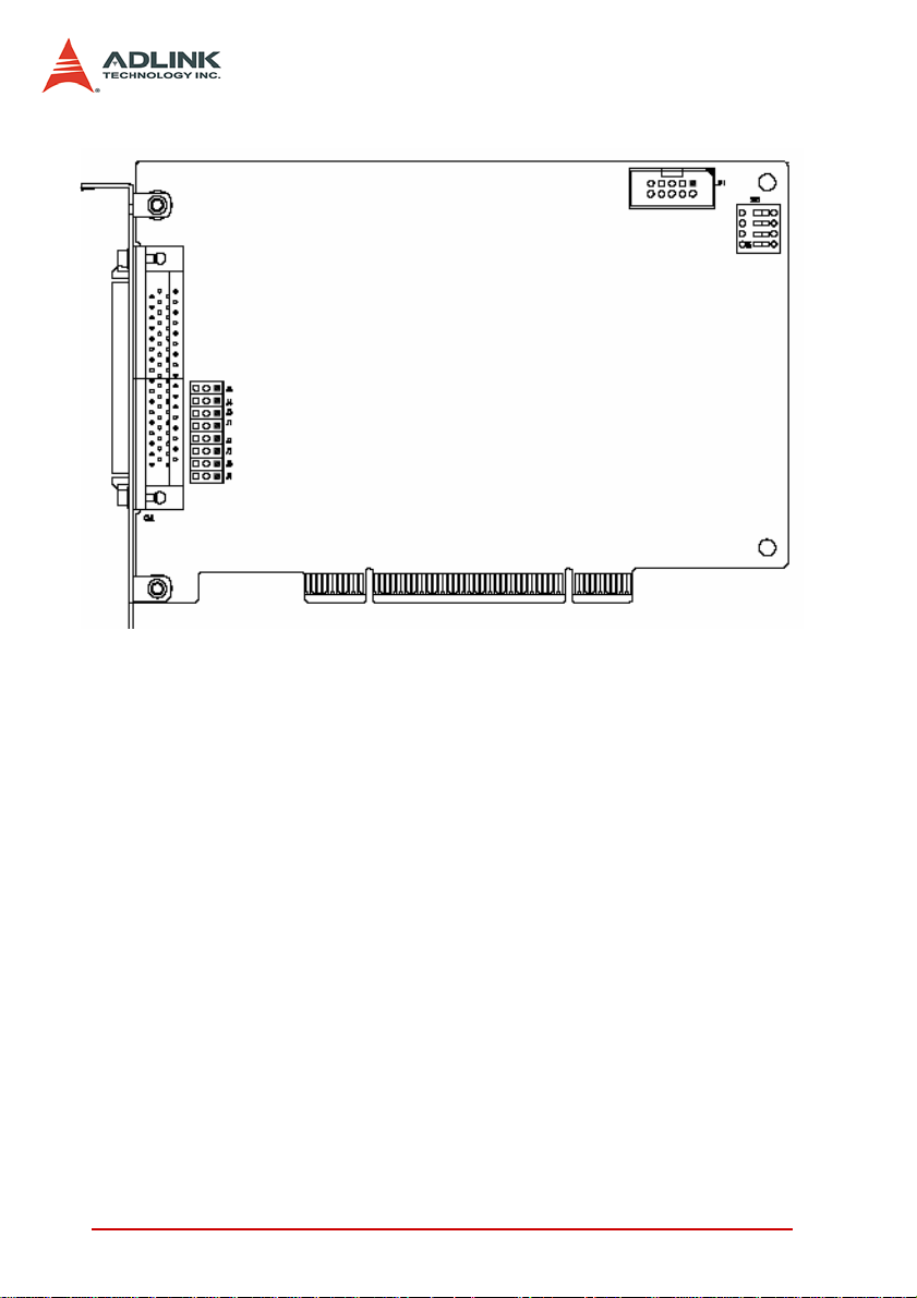
2.2 PCI-8144 Outline Drawing
Figure 2-1: PCB Layout of the PCI-8144
X CN1: Input/Output signal connector
X JP2: Direct control to stepper
X SW1: Card ID selection
X J1-J8: Pulse output selection jumper
10 Installation
Page 21

2.3 PCI-8144 Hardware Installation
2.3.1 Hardware configuration
The PCI-8144 is fully Plug-and-Play compliant. Hence, memory
allocation (I/O port locations) and IRQ channel of the PCI card are
assigned by the system BIOS. The address assignment is done
on a board-by-board basis for all PCI cards in the system.
2.3.2 PCI slot selection
Some computer system may hav e both PC I and ISA slots. Do not
force the PCI card into a PC/AT slot. The PCI-8144 can be used in
any PCI slot.
2.3.3 Installation Procedures
1. Read through this manual and setup the jumper according to your application
2. Turn off your computer. Turn off all accessories (printer,
modem, monitor, etc.) connected to computer. Remove
the cover from the computer.
3. Select a 32-bit PCI expansion slot. PCI slots are shorter
than ISA or EISA slots and are usually white or ivory.
4. Before handling the PCI-8144, discharge any static
buildup on your body by touching the metal case of the
computer. Hold the edge of the card and do not touch
the components.
5. Position the board into the PCI slot you have selected.
6. Secure the card in place at the rear panel of the system
unit using screws removed from the slot.
2.3.4 Troubleshooting:
If your system doesn’t boot or if you experience erratic operation
with your PCI board in place, it’s most likely caused by an interrupt
conflict (possibly an incorrect ISA setup). In general, the solution,
once determined it is not a simple oversight, is to consult the BIOS
documentation that comes with your system.
Installation 11
Page 22

Check the control panel of the Windows system if the card is listed
by the system. If not, check the PCI settings in the BIOS or use
another PCI slot.
12 Installation
Page 23

2.4 Software Driver Installation
1. Auto run the ADLINK All-In-One CD. Choose Driver
Installation -> Motion Control -> PCI-8144.
2. Follow the procedures of the installer.
3. After setup installation is completed, restart windows.
Note: Please download the latest software from ADLINK website if
necessary.
2.5 SW1 Card Index Selection
The SW1 switch is used to set the card index. For example, if 1 is
set to ON and the others are OFF, that card index is 1. The index
value can be from 0 to 15. Refer to the following table for details.
Card ID Switch Setting (ON=1)
00000
10001
20010
3 0011
40100
50101
60110
7 0111
81000
91001
10 1010
11 1011
12 1100
13 1101
14 1110
15 1111
Table 2-1: SW1 Card Index
Installation 13
Page 24
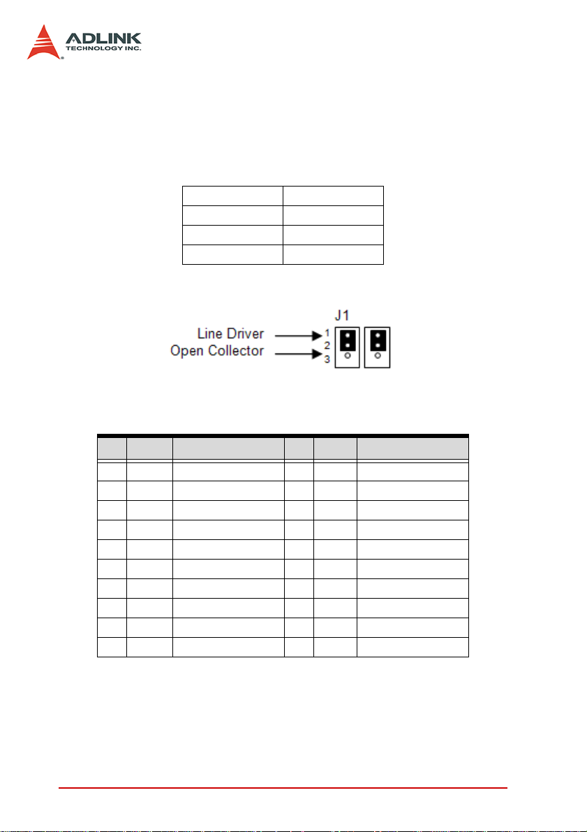
2.6 J1-J8 Pulse Output Type: Differential / Open Collector
Jumpers J1-J8 are used to set the ty pe of pulse output signals.
The output signal type can either be differential line driver or open
collector output. Refer to section 3.1 for detail jumper settings.
J1 & J2 Axis 0
J3 & J4 Axis 1
J5 & J6 Axis 2
J7 & J8 Axis 3
2.7 JP2 Direct Control to Stepper
No. Name Function No. Name Function
1 DGND Bus power ground 2 PB4 Axis 3 Pulser PHB
3 PA4 Axis 4 Pulser PHA 4 PB3 Axis 2 Pulser PHB
5 PA3 Axis 3 Pulser PHA 6 VCC Bus Power +5V
7 DGND Bus power ground 8 PB2 Axis 1 Pulser PHB
9 PA2 Axis 1 Pulser PHA 10 PB1 Axis 0 Pulser PHB
11 PA1 Axis 0 Pulser PHA 12 VCC Bus Power +5V
13 -- N/A 14 -- N/A
15 -- N/A 16 -- N/A
17 -- N/A 18 -- N/A
19 -- N/A 20 -- N/A
Table 2-2: JP2 Direct Control to Stepper
14 Installation
Page 25

2.8 CN1 Pin Assignments: Main connector
CN1 is the major connector for the motion control I/O signals.
No. Name I/O Function No. Name I/O Function
1 VDD O I solated +5V Output 35 VDD O Isolated +5V Output
2 EGND - Ext. power ground 36 EGND - Ext. power ground
3 CW+ O Positive pulse (+) 37 CW+ O Positive pulse (+)
4 CW- O Positive pulse (-) 38 CW- O Positive pulse (-)
5 CCW+ O Negative pulse (+) 39 CCW+ O Negative pulse (+)
6 CCW- O Negative pulse (- ) 40 CCW- O Negative pulse (-)
7 PEL0 I Positive end limit signal 41 PEL2 I Positive end limit signal
8 MEL0 I Negative end limit signal 42 MEL2 I Negative end limit signal
9 PSD0 I Positive slow down signal 43 PSD2 I Positive slow down signal
10 MSD0 I Negative slow down signal 44 MSD2 I Negative slow down signal
11 ORG0 I Origin signal 45 ORG2 I Origin signal
12 EGND - Ext. power ground 46 EGND - Ext. power ground
13 CW+ O Positive pulse (+) 47 CW+ O Positive pulse (+)
14 CW- O Positive pulse (-) 48 CW- O Positive pulse (-)
15 CCW+ O Negative pulse (+) 49 CCW+ O Negative pulse (+)
16 CCW- O Negative pulse (-) 50 CCW- O Negative pulse (-)
17 PEL1 I Positive end limit signal 51 PEL3 I Positive end limit signal
18 MEL1 I Negative end limit signal 52 MEL3 I Negative end limit signal
19 PSD1 I Positive slow down signal 53 PSD3 I Positive slow down signal
20 MSD1 I Negative slow down signal 54 MSD3 I Negative slow down signal
21 ORG1 I Origin signal 55 ORG3 I Origin signal
22 STP/EMG I Forced stop signal 56 STA I External start signal
23 DIN0 I Digital Input 0 57 DOUT0 O Digital Output 0
24 DIN1 I Digital Input 1 58 DOUT1 O Digital Output 1
25 DIN2 I Digital Input 2 59 DOUT2 O Digital Output 2
26 DIN3 I Digital Input 3 60 DOUT3 O Digital Output 3
27 DIN4 I Digital Input 4 61 DOUT4 O Digital Output 4
28 DIN5 I Digital Input 5 62 DOUT5 O Digital Output 5
29 DIN6 I Digital Input 6 63 DOUT6 O Digital Output 6
30 DIN7 I Digital Input 7 64 DOUT7 O Digital Output 7
31 VDD - Isolated +5V Output 65 DO_COM - Common for DO
32 VDD - Isolated +5V Output 66 DO_COM - Common for DO
33 EGND - Ext. power ground 67 EGND - Ext. power ground
34 EX+24V I +24V isolation power input 68 EX+24V I +24V isol ation power input
Table 2-3: CN1 Pin Assignments
Installation 15
Page 26

16 Installation
Page 27

3 Signal Connections
Signal connections of all I/O’s are described in this chapter. Refer
to the contents of this chapter before wiring any cables between
the PCI-8144 and any stepper drivers.
This chapter contains the following sections:
Section 3.1 Pulse Output Signals CW and CCW
Section 3.2 Orig in Sign al ORG
Section 3.3 Slow Down input signal
Section 3.4 End- Lim it Signa ls PEL an d MEL
Section 3.5 Simultaneous start/stop signals STA and STP
Section 3.6 Termination Board
Section 3.7 General-purposed DIO
Section 3.8 JP2 pin definition for stepping singal (Optional)
Signal Connections 17
Page 28

3.1 Pulse Output Signals CW and CCW
There are 4 axis pulse output signals on the PCI-8144. For each
axis, two pairs of CW and CCW signals are used to transmit the
pulse train and to indicate the direction. In this section, the electrical characteristics of the CW and CCW signals are detailed. Each
signal consists of a pair of differential signals. For example, CW2
consists of CW2+ and CW2- signals. The following table shows all
pulse output signals on CN1.
CN1 Pin No. Signal Name Description Axis #
3 CW0+ Pulse signals (+) 1
4 CW0- Pulse signals (-) 1
5 CCW0+ Direction signal (+) 1
6 CCW0- Direction signal (-) 1
13 CW1+ Pulse signals (+) 2
14 CW1- Pulse signals (-) 2
15 CCW1+ Direction signal (+) 2
16 CCW1- Direction signal (-) 2
17 CW2+ Pulse signals (+) 3
18 CW2- Pulse signals (-) 3
39 CCW2+ Direction signal (+) 3
40 CCW2- Direction signal (-) 3
47 CW3+ Pulse signals (+) 4
48 CWT3- Pulse signals (-) 4
49 CCW3+ Direction signal (+) 4
50 CCW3- Direction signal (-) 4
18 Signal Connections
Page 29
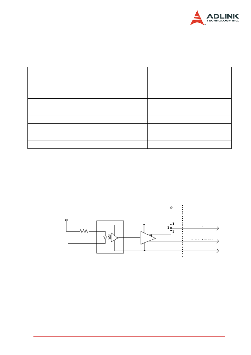
The output of the CW or CCW signals can be configured by jumpers as either differential line drivers or open collector output. Users
can select the output mode either by closing breaks between 1
and 2 or 2 and 3 of jumpers J1-J8 as follows:
Output Signal
CW0- J1 J1
CCW0- J2 J2
CW1- J3 J3
CCW1- J4 J4
CW2- J5 J5
CCW2- J6 J6
CW3- J7 J7
CCW3- J8 J8
For differential line driver output,
close breaks between 1 and 2 of:
For open collector output, close
breaks between 2 and 3 of:
The default setting of CW and CCW is set to differ ential line driver
mode.
The following wiring diagram is for CW and CCW signals on the 4
axes.
PCI-8144:
J1~J8
VDD
CW+, CCW+
CW-, CCW-
CW/CCW
D5V
HP0631
R
26LS31
EGND
Note: If the pulse output is set to open collector output mode, CW-
and CCW- are used to transmit CW and CCW signals. The
sink current must not exceed 20mA on the CW- and CCWpins. The default setting of jumper is 1-2 shorted.
Suggest Usage: Jumper 2-3 shorted and conn ect CW+/CCW+ to
a 470 ohm pulse input interface’s COM of driver. See the following
figure.
Signal Connections 19
Page 30
Choose one of CW/CCW+ and CW/CCW- to connec t to driver’s
OUT/DIR
Warning: The sink current must not exc eed 20mA or t he 2631 will
be damaged!
20 Signal Connections
Page 31

3.2 Origin Signal ORG
The origin signals (ORG1-ORG4) are used as input signals for the
origin of the mechanism. The following table lists signal names,
pin numbers, and axis numbers:
CN1 Pin No Signal Name Axis #
11 ORG0 1
21 ORG1 2
45 ORG2 3
55 ORG3 4
The input circuit of the ORG signals is shown below. Usually, a
limit switch is used to indicate the origin on one axis. The specifications of the limit switch should have contact capacity of +24V @
10mA minimum. An internal filter circuit is used to filter out any
high frequency spikes, which may cause errors in the operation.
When the motion controller is operated in the home return mode,
the ORG signal is used to inhibit the control output signals (CW
and CCW). For detailed operations of the ORG signal, refer to
Section 4.
Signal Connections 21
Page 32

3.3 Slow Down input signal
The PCI-8144 provides slow down function through SD input pin.
The signal names, pin numbers, and axis numbers are shown in
the following table:
CN1 Pin No Signal Name Axis # CN1 Pin No Signal Name Axis #
9 PSD0 1 43 PSD2 3
10 MSD0 1 44 MSD2 3
19 PSD1 2 53 PSD3 4
20 MSD1 2 54 MSD3 4
The SD input pin wiring diagram is as follows:
22 Signal Connections
Page 33

3.4 End-Limit Signals PEL and MEL
There are two end-limit signals PEL and MEL for each axis. PEL
indicates the end limit signal is in the plus direction and ME L indicates the end limit signal is in the minus direction. The signal
names, pin numbers, and axis numbers are shown in the table
below:
CN1 Pin No Signal Name Axis # CN1 Pin No Signal Name Axis #
7 PEL0 1 41 PEL2 3
8 MEL0 1 42 MEL2 3
17 PEL1 2 51 PEL3 4
18 MEL1 2 52 MEL3 4
A circuit diagram is shown in the diagram below. The external limit
switch should have a contact capacity of +24V @ 10mA minimum.
EL logical can be configured by registers controlling. For more
details on EL operation, refer to Section 4.
Signal Connections 23
Page 34

3.5 Simultaneously Start/Stop Signals STA and STP
The PCI-8144 provides STA and STP signals, which enable simultaneous start/stop of motions on multiple axes. The STA and STP
signals are on CN1, STP @ pin 22 and STA @ pin 56.
The diagram below shows the onboard circuit. The STA and STP
signals of the four axes are tied together respectively.
The STP and STA signals are input signals. To operate the start
and stop action simultaneously, both software control and external
control are needed. With software control, the signals must be
generated from external event to the chip of PCD4541. Users can
also use an external open collector or switch to drive the STA/STP
signals for simultaneous start/stop.
If there are two or more PCI-8144 cards, tie all STA and all STP
signals of all cards resepectively for simultaneous start/stop control on all concerned axes. In this case, connect CN1 as below:
24 Signal Connections
Page 35

3.6 Termination Board
CN1 of the PCI-8144 can be connected with a DIN-68S, including
the ACL-10569-1 cable (a 68-pin SCSI-SCSI cable). The DIN-68S
is a general purpose 68-pin SCSI-II DIN-socket. It has easy wiring
screw terminals and an easily installed DIN socket that can be
mounted onto the DIN rails
3.7 General Purpose DIO
PCI-8144 has 8 opto-isolated digital outputs and 8 open collector
digital inputs for general purpose use. Pin assignments are illustrated in the table below:
CN1 Pin No Signal Name CN1 Pin No Signal Name
23 DIN0 57 DOUT0
24 DIN1 58 DOUT1
25 DIN2 59 DOUT2
26 DIN3 60 DOUT3
27 DIN4 61 DOUT4
28 DIN5 62 DOUT5
29 DIN6 63 DOUT6
30 DIN7 64 DOUT7
65 DO_COM
66 DO_COM
Signal Connections 25
Page 36

3.7.1 Isolated Input channels
3.7.2 Isolated Output channels
3.7.3 Example of input connection
DIN
26 Signal Connections
Page 37

3.7.4 Example of output connection
3.8 JP2 pin define for stepping singal (Optional)
Signal Connections 27
Page 38

PCI-8144 provides another optional JP2 pins for stepping motor
signal. Pin definitions of JP2 and connection example are
described as follow:
JP2 Pin No Signal Name JP2 Pin No Signal Name
10
12
14
16
2
4
6
8
Φ2x
Φ4x
Φ2y
Φ4y
Φ2z
Φ4z
Φ2u
Φ4u
11
13
15
1
3
5
7
9
Φ1x
Φ3x
Φ1y
Φ3y
Φ1z
Φ3z
Φ1u
Φ3u
Pins 17 to 26 are not used
Connection example:
28 Signal Connections
Page 39

4 Operation Theory
This chapter describes the detail operation of the motion controller
card. Contents of the following sections are as follows:
Section 4.1: Classifications of Motion Controller
Section 4.2: Motion Control Modes
Section 4.3: M ot or Drive r Int er face
Section 4.4: M ec ha n ical switch Interface
Section 4.5: T he Cou n ter s
Section 4.6: The Comparators
Section 4.7: Other Motion Functions
Section 4.8: Interrupt Control
Section 4.9: Multiple Cards Operation
4.1 Classifications of Motion Controller
When motor/stepper control first started, motion control was
widely discussed instead of motor control. Motor control was separated into two layers: motor control and motion control. Motor control relates to PWM, power stage, closed loop, hall sensors, vector
space, etc. Motion control relates to speed profile generating, trajectory following, multi-axes synchronizat ion , an d co ordin a ting .
4.1.1 Voltage motion control interface
The interfaces between motion and motor control are changing
rapidly. Early on, a voltage singal was used as a command to the
motor controller. The amplitude of the signal means how fast a
motor is rotating and the time duration of the voltage changes
means how fast a motor acceleration from one speed to the other
speed. Voltage signal as a command to motor driver is so called
“analog” motion controller. It is much eaiser to integrate into an
analog circuit of motor controller; however noise is sometimes a
big problem for this type of motion control. Also, to do positioning
control of a motor, the analog motion controller must ha ve a feedback signal with position information and use a closed loop control
algorithm to make it possible. This increased the complexity of
motion control and not easy to use for a beginner.
Operation Theory 29
Page 40

4.1.2 Pulse motion control interface
The second interface of motion and motor control is a pulse train
type. As a trend of digital world, pulse trains represent a new concept to motion control. The counts of pulses show how many ste ps
of a motor rotates and the frequency of pulses show how fast a
motor runs. The time duration of frequency changes represent the
acceleration rate of a motor. Because of this interface, a servo or
stepper motor can be easier than an analog type for positioning
applications. It means that motion and motor control can be separated more easily by this way.
Both of these two interfaces need to provide for gains tuning. For
analog position controllers, the control loops are built inside and
users must tune the gain from the controller. For pulse type position controllers, the control loops are built outside on the motor
drivers and users must tune the gains on drivers.
For more than one axes’ operation, motion control seems more
important than motor control. In industial applications, reliable is a
very important factor. Motor driver vendors make good performance products and a motion controller vendors make powerful
and variety motion software. Integrated two products make our
machine go into perfect.
4.1.3 Network motion control interface
Recently, there was a new control interface was introduced--a network motion controller. The command between motor driver and
motion controller is not analog or pulses signal any more. It is a
network packet which contents position information and motor
information. This type of controller is more reliable because it is
digitized and packetized. Because a motion controller must be
real-time, the nerowrk must have real-time capacity around a cycle
time below 1 mini-second. This means that non-commercial networks cannot do this job. It must have a specific network, such as
Mitsubishi SSCNET. The network may also be built with fiberoptics
to increase communication reliability.
30 Operation Theory
Page 41

4.1.4 Software real-time motion control kernel
For motion control kernel, there are three ways to accomplish it:
DSP, ASIC, and software real-time.
A motion control system needs an absolutely real-time control
cycle and the calculation on controller must provide a control data
at the same cycle. If not, the motor will not run smoothly. Many
machine makers will use PC’s computing power to do this. A feedback counter card can simply be used and a voltage output or
pulse output card to make it. This method is very low-end and
takes much software effort. For sure their realtime performance,
they will use a real-time software on the system. It increases the
complexity of the system too. But this method is the most flexible
way for a professional motion control designers. Most of these
methods are on NC machines.
4.1.5 DSP motion control kernel
A DSP-based motion controller kernel solves real-time software
problem on computer. DSP is a micro-processer itself and all
motion control calculations can be done on it. There is no real-time
software problem because DSP has its own OS to arrange all the
procedures. There is no interruption from other inputs or context
switching problem like Windows based computer. Although it has
such a perfect performance on real-time requirements, its calculation speed is not as fast as PC’s CPU at this age. The software
interfacing between DSP controller’s vendors and users is not
easy to use. Some controller vendors provide some kind of
assembly languages for users to learn and some controller vendors provide only a handshake documents for users to use. Both
ways are not easy to use. DSP based controller provide a bette r
way than software kernel for machine makers to build they applications.
4.1.6 ASIC motion control kernel
An ASIC motion control kernel is falls between software kernel
and DSP kernel in terms of difficulty. It has no real-time problem
because all motion functions are done via the ASIC. Users or controller’s vendors just need to set some parameters which the ASIC
requires and the motion control will be done easily. This kind of
Operation Theory 31
Page 42

motion control separates all system integration problems into 4
parts: Motor driver’s performance, ASIC outputting profile, vendor’s software parameters to the ASIC, and users’ command to
vendors’ software. It makes motion controller co-operated more
smoothly between devices.
4.1.7 Compare Table of all motion control types
Software ASIC DSP
Price Fair Cheap Expensive
Functionality Highest Low Normal
Maintenance Hard Easy Fair
Analog Pulses Network
Price High Low Normal
Signal Quality Fair Good Reliable
Maintenance Hard Easy Easy
4.1.8 PCI-8144 motion controller type
The PCI-8144 is an ASIC based, pulse type motion controller
made into three blocks: motion ASIC, PCI card, software motion
library. The motion ASIC can be accessed via our software motion
libray under many kinds of Windows NT/2000/XP, Linux, and RTX
driver. Our software motion library provides one-stop-function for
controlling motors. All the speed parameter calculations are done
via our library.
For example, to perform a one-axis point to point moition with a
trapezoidal speed profile, only fill the target position, speed, and
acceleration time in one function. Then the motor will run as the
profile. It takes no CPU resources because every control cycle
pulse generation is done by the ASIC. The precision of target position depends on motor drivers’ closed loop control performance
and mechnical parts, not on motion controller’s command because
the motion controller is only responsible for sending correct pulses
counts via a desired speed profile. So it is much e asier for programmers, mechnical or electrical engineers to find out problems.
32 Operation Theory
Page 43

4.2 Motion Control Modes
Motion control makes the motors run according to a specific speed
profile, path trajectory and synchronous condition with other axes.
The following sections describe the motion control modes of this
motion controller could be performed.
4.2.1 Coordinate system
The Cartesian coordinate is used and pulses are in the unit of
length. The physical length depends on mechanical parts and
motor’s resolution. For example, if a motor is on a screw ball, and
the pitch of screw ball is 10mm and the pulses needed for a round
of motor are 10,000 pulses. One pulse’s physical unit is equal to
10mm/10,000p =1 mm.
Just set a command with 15,000 pulses for motion controller if we
want to move 15mm. How about if we want to move 15.0001mm?
Simple! The motion controller will keep the residue value less
than 1 pulse and add it to next command.
The motion controller sends incremental pulses to motor drive rs. It
means that we can only send relative command to motor driver.
But we can solve this problem by calculating the difference
between current position and target position first. Then send the
differences to motor driver. For example, if current position is 1000
and we want to move a motor to 9000, you can use an absolute
command to set a target position of 9000. Inside the motion controller, it will get current position 1000 first then calculate the difference from target position. The result is +8000. So, the motion
controller will send 8000 pulses to motor driver to move the position of 9000.
Sometimes, users need to install a linear scale or external
encoder to check machine’s position. But how do you to build this
coordinate system? If the resolution of external encoder is 10,000
Operation Theory 33
Page 44

pulses per 1mm and the motor will move 1mm if the motion controller send 1,000 pulses, It means that when we want to move 1
mm, we need to send 1,000 pulses to motor driver then we will get
the encoder feedback value of 10,000 pulses. If we want to use an
absolute command to move a motor to 10,000 pulses position and
current position read from encoder is 3500 pulses, how many
pulses will it send to motor driver? The answer is (10000 – 3500 ) /
(10,000 / 1,000)=650 pulses. The motion controller will calculate it
automatically if users set “move ratio” already. The “move ratio”
means the (feedback resolution/command resolution)
Note: The PCI-8144 provides only one dimension motion function.
4.2.2 Absolute and relative position move
In the coordinate system, we have two kinds command for users
to locate the target position. One is absolute and the other is relative. Absolute command means that user give the motion controller a position, then the motion controller will move a motor to that
position from current position. Relative command means that user
give the motion controller a distance, then the motion controller
will move motor by the distance from current position. During the
movement, users can specify the speed profile. It means user can
define how fast and at what speed to reach the position.
The PCI-8144 provides only relative position move because it
is designed for stepper motor. It is meaningless for a stepper
motor controller to have the encoder feedback interface for absolute motion.
34 Operation Theory
Page 45

4.2.3 Trapezoidal speed profile
Trapezodial speed profile means the acceleration/deceleration
area follows a 1st order linear velocity profile (constant acceleration rate). The profile chart is shown as below:
The area of the velocity profile represents the distance of this
motion. Sometimes, the profile looks like a triangle because the
desired distance from user is smaller than the area of given speed
parameters. When this situation happens, the motion controller
will lower the maximum velocity but keep the acceleration rate to
meet user’s distane requirement. The chart of this situation is
shown as below:
This kind of speed profile could be applied on velocity mode, position mode in one axis or multi-axes linear interpolation and two
axes circular interpolation modes.
The PCI-8144 Tacc and Tdec are always the same.
Operation Theory 35
Page 46

4.2.4 S-curve and Bell-curve speed profile
S-curve means the speed profile in accelerate/decelerate area follows a 2nd order curve. It ca n reduce vibration at the beginning of
motor start and stop. In order to speed up the acceleration/deceleration during motion, we need to insert a linear part into these
areas. We call this shape as “Bell” curve. It adds a linear curve
between the upper side of s-curve and lower side of s-curve. This
shape improves the speed of acceleration and also reduces the
vibration of acceleration.
a) For a purse S-curve, we define its shape ’ s parameter as below:
X Tacc: Acceleration time in second
X Tdec: Deceleration time in second
X StrVel: Starting velocity in PPS
X MaxVel: Maximum velocity in PPS
The PCI-8144 Tacc and Tdec are always the same.
36 Operation Theory
Page 47

b) For a bell curve, we define its shape parameters as below: (the
PCI-8144 dosen’t support this mode)
X Tacc: Acceleration time in second
X Tdec: Deceleration time in second
X StrVel: Starting velocity in PPS
X MaxVel: Maximum velocity in PPS
X VSacc: S-curve part of a bell curve in deceleration in PPS
X VSdec: S-curve part of a bell curve in deceleration in PPS
If VSacc or VSdec=0, it means acceleration or deceleration use
pure S-curve without linear part. The Acceleration chart of bell
curve is shown below:
Operation Theory 37
Page 48

4.2.5 Velocity mode
Veloctiy mode means the pulse command is continuously outputing until a stop command is issued. The motor will run without a
target position or desired distance unless it is stopped by other
reasons. The output pulse accelerates from a starting velocity to a
specified maximum velocity. It can be follow a linear or S-curve
acceleration shape. The pulse output rate is kept at maximum
velocity until another velocity command is set or a stop command
is issued. The velocity could be overrided by a new speed setting.
Notice that the new speed could not be a reversed speed of original running speed. The speed profile of this kind of motion is
shown as below:
38 Operation Theory
Page 49

4.2.6 One axis position mode
Position mode means the motion controller will output a specific
amount of pulses which is equal to users’ desired position or distance. The unit of distance or position is pulse internally on the
motion controller. The minimum length of distance is one pulse.
However, in PCI-8144, we provide a floating point function for
users to transform a physical length to pulses. Inside our software
library, we will keep those distance less than one pulse in register
and apply them to the next motion function. Besides positioning
via pulse counts, our motion controller provides three types of
speed profile to accomplish positioning. There are 1st order trapezoidal, 2nd order S-curve, and mixed bell curve. Users can call
respective functions to perform that. The following char shows the
relationship between distance and speed profile. We use trapezoidal shape to show it.
The distance is the area of the V-t diagram of this profile.
The PCI-8144 Tacc and Tdec are always the same.
Operation Theory 39
Page 50

4.2.7 Home Return Mode
Home return means searching a zero p osition po int on the co ordinate. Sometimes, users use ORG pin as a zero position on the
coordinate. At the beginning of machine power on, the program
needs to find a zero point of this machine. Our motion controller
provides following functions to make it.
_8144_enable_sd_signal
_8144_enable_org_stop,
_8144_tv_move,
_8144_sv_move.
When ORG signal control is enabled (home return operation), the
ORG signal is turned ON and the motor will stop immediately.
After that, if the ORG signal goes OFF, the motor will remain
stopped. Those signal statues can be used by the function,
“_8144_get_mio_status”.
X When SD is not installed
X When SD is installed and SD is not latched
40 Operation Theory
Page 51

Example.
_8144_enable_sd_signal( AxisNo, Enable); //Enable
SD signal control
_8144_enable_org_stop( AxisNo, Enable); //Enable
ORG signal stop
_8144_sv_move(AxisNo, StrVel, MaxVel, Tacc); //
perform a sv-move
4.2.8 Synchronous Start Function
Synchronous motion means more than one axis can be started by
a synchronous signal (STA) which could be external or internal
signals. For external signal, users must set move parameters first
for all axes then these axes will wait an extern start/stop command
to start or stop. For internal signal, the start command could be
from a software start function. Once it is issued, all axes which are
in waiting synchronous mode will start at the same time.
The PCI-8144 card suports external start function. When the user
sets the external start by _8144_external_start function for each
axis which the user want to perform external start, then set the
move function for those axes. Thoes axis will start at the same
time when STA signal goes ON.
Operation Theory 41
Page 52

4.2.9 Auto Home Move Mode
Depending on the software homing mode design, the PCI-8144
offers an auto homing move function which means the axis will
move to a zero position point on the coordinate. This mod e is used
to add an auto home moving function on the normal home return
mode described in the previous section no matter which position
the axis is. The following diagram shows an example for normal
home mode usage for which the start point is between the ORG
and EL signal or exists in the ORG signal. The ORG offset can’t b e
zero because the motion ASIC of the PCI-8144 offers a level trigger for the ORG signal. The suggested value is the double length
of the ORG area. A homing status function can be used to monitor
the current status of the homing operation .
Case 1: SD (Slow down)
Case 2: EL (End Limit)
Case 3: Inversed direction moving
(Slow down)
Case 4: Stop at ORG
Case 5: SD (Slow down)
Case 6: EL (End Limit)
Case 7: Inversed dir ect ion movin g
(Slow down)
> Stop at ORG
> SD (Slow down) > Stop at ORG
> EL (End Limit) > Return > SD
> Stop at ORG
> Stop at ORG
> SD (Slow down) > Stop at ORG
> EL (End Limit) > Return > SD
> Stop at ORG
42 Operation Theory
Page 53

Case 1
Case 2
Case 3
Case 4
Case 5
Case 6
Case 7
SD signal
ORG signal
EL signal
Operation Theory 43
Page 54

4.3 The motor driver interface
We provide several dedicated I/Os which can be connected to
motor driver directly and have their own functions. Motor drivers
have many kinds of I/O pins for external motion controller to use.
We classify them to two groups. One is pulse I/O signals including
pulse command and encoder interface. The other is digital I/O signals including servo ON, alarm, INP, servo ready, alarm reset and
emergency stop inputs. The following sections will describe the
functions these I/O pins.
The PCI-8144 has only pulse command interface.
4.3.1 Pulse Command Output Interface
The motion controller uses pulse command to control servo/stepper motors via motor drivers. Please set the drivers to position
mode which can accept pulse trains as position command. The
pulse command consists of two signal pairs. It is defined as CW
and CCW pins on connector . Each signal has two p ins as a pair for
differential output.
Dual Pulse Output Mode (CW/CCW Mode)
The waveform of the CW and CCW pins represent CW (clockwise) and CCW (counter clockwise) pulse ou tput respectively.
The numbers of pulse represent distance in pulse. The frequency of the pulses represents speed in pulse per second.
Pulses output from the CW pin makes the motor move in positive direction, whereas pulse output from the CCW pin makes
the motor move in negative direction. The following diagram
shows the output waveform of positive (+) commands and negative (-) commands.
44 Operation Theory
Page 55

Pulse outmode = 0: (Pulse is normally high)
Pulse outmode = 1: (Pulse is normally low)
The command pulses are counted by a 24-bit preset countdown
counter. The preset counter can store a value of total pulses outputting from controller.
Operation Theory 45
Page 56

4.4 Mechanical switch interface
We provide some dedicated input pins for mechanical switches
like original switch (ORG), plus and minus end-limit switch (
slow down switch (SD). These switches’ response time is very
fast, only a few ASIC clock times. There is no re al-time problem
when using these signals. All functions are done by motion ASIC.
The software can just do nothing an d o nly need to wait the resu lts.
4.4.1 Original or home signal
Our controller provides one original or home signal for each axis.
This signal is used for defining zero position of this axis. The logic
of this signal must be set properly before doing home procedure.
Please refer to home mode section for details.
4.4.2 End-Limit switch signal
The end-limit switches are usually installed on both ending sides
of one axis. We must install plus EL at the positive position of the
axis and minus EL at the negative position of the axis. These two
signals are for safty reason. If they are installed reversely, the protection will be invalid. Once the motor’s moving part touches one
of the end-limit signals, the motion controller will stop sending
pulses and output an ERC signal. It can prevent machine crash
when miss operation.
±EL),
4.4.3 Slow down switch
The slow down signals are used to force the command pulse to
decelerate to the starting velocity when it is active. This signal is
used to protect a mechanical moving part under hig h speed movement toward the mechanism’s limit. The SD signal is effective for
both plus and minus directions.
46 Operation Theory
Page 57

4.5 The Counters
4.5.1 Preset Command position counter
The preset command position counter is a 24-bit binary downcount counter. It provides the information of the current command
counts which are not outputted.
4.6 Interrupt Control
The motion controller can generate an interrupt signal to the host
PC. It is much useful for event-driven software application. There
are two kinds of interrupt sources on PCI-8144. One is motion
interrupt source and the other is GPIO interrupt sources. Motion
and GPIO interrupt sources can be maskable. Motion interrupt
sources can be maskable by
_8144_set_motion_interrupt_factor(). Its mask bits are
shown as following table:
Motion Interrupt Source Bit Settings (1=Enable,0=Disable)
Bit Description
0 Motion Stop
1-15 (reserve)
Operation Theory 47
Page 58

The GPIO interrupt sources are maskable. The mask bits table is
shown below:
GPIO Interrupt Source Bit Settings (1=Enable,0=Disable)
Bit Description
0 DI0 falling edge
1 DI1 falling edge
2 DI2 falling edge
3 DI3 falling edge
4 DI4 falling edge
5 DI5 falling edge
6 DI6 falling edge
7 DI7 falling edge
8 DI0 rising edge
9 DI1 rising edge
10 DI2 rising edge
11 DI3 rising edge
12 DI4 rising edge
13 DI5 rising edge
14 DI6 rising edge
15 DI7 rising edge
After seting the factors of interrupt, users can use wait functions to
wait the interrupts, it uses no processor time while waiting for the
specified interrupt to become signaled or the time-out interval to
elapse.
48 Operation Theory
Page 59

The steps for using interrupts:
1. Set interrupt sources for Motion or GPIO interrupts.
_8144_set_motion_interrupt_facor(AXIS0, 0x01);
// Axis0 stop
_8144_set_gpio_interrupt_factor(CARD0, 0x01);
// DI0 falling edge
2. Using wait function to wait the specified interrupt
_8144_wait_single_motion_interrupt(AXIS0, 0x01,
1000);
// Wait 1000ms for normally stop interrupt
_8144_wait_single_gpio_interrupt(CARD0, 0x01,
1000)
// Wait 1000ms for DI0 falling edge
interrupt
3. Disable interrupt sources
_8144_set_motion_interrupt_facor(AXIS0, 0x0);
_8144_set_gpio_interrupt_factor(CARD0, 0x0);
Operation Theory 49
Page 60

4.7 Multiple Card Operation
The motion controller allows more than one card in one system.
Since the motion controller is plug-and-p lay compatible, the base
address and IRQ setting of the card are automatically assigned by
the PCI BIOS at the beginning of system booting. Users don’t
need and can’t change the resource settings.
When multiple cards are applied to a system, the number of card
must be noted. The card number depends on the card ID switch
setting on the the board. The axis number is depends on the card
ID. For example, if three motion controller cards are plugged in to
PCI slots, and the corresponding card ID is set, then the axis number on each card will be:
Axis No. X Y Z U
Card ID
0 0123
2 891011
3 12 13 14 15
Notice that if there has the same card ID on multiple cards, the
function will not work correctly.
50 Operation Theory
Page 61

5 MotionCreatorPro
After installing the hardware (Chapters 2 and 3), it is necessary to
correctly configure all cards and double check the system before
running. This chapter gives guidelines for establishing a control
system and manually testing the 8144 cards to verify correct operation. The MotionCreatorPro software provides a simple yet powerful means to setup, configure, test, and debug a motion control
system that uses 8144 cards.
Note that MotionCreatorPro is only available for Windows 2000/
XP with a screen resolution higher than 1024x768. Recommended
screen resolution is 1024x768. It cannot be executed under the
DOS environment.
5.1 Run MotionCreatorPro
After installing the software drivers for the 8144 in Windows 2000/
XP, the MotionCreatorPro program can be located at <chosen
path> \PCI-Motion\MotionCreatorPro. To execute the program,
double click on the executable file or use Start>Program
Files>PCI-Motion>MotionCreatorPro.
MotionCreatorPro 51
Page 62

5.2 About MotionCreatorPro
Before Running MotionCreatorPro, the following issues should be
kept in mind.
1. MotionCreatorPro is a prog ram written in VB.NET 2003,
and is available only for Windows 2000/XP with a screen
resolution higher than 1024x768. It cannot be run under
DOS.
2. MotionCreatorPro allows users to save settings and configurations for 8144 cards. Saved configurations will be
automatically loaded the next time MotionCreatorPro is
executed. Two file s, 8144.ini and 8144MC.ini, in the
windows root directory are used to save all settings
and configurations.
3. To duplicate configurations from one system to another,
copy 8144.ini and 8144MC.ini into the windows root
directory.
4. If multiple 8144 cards use the same MotionCreatorPro
saved configuration files, the DLL function call
_8144_config_from_file() can be invoked within a
user developed program. This function is available in a
DOS environment as well.
52 MotionCreatorPro
Page 63

5.3 MotionCreatorPro Form Introducing
5.3.1 Main Menu
The main menu appears after running Motion CreatorPro. It is used
to:
MotionCreatorPro 53
Page 64

5.3.2 Select Menu
The select menu appears after running MotionCreatorPro. It is
used to:
54 MotionCreatorPro
Page 65

5.3.3 Card Information Menu
This menu shows Information about this card.
MotionCreatorPro 55
Page 66

5.3.4 Configuration Menu
In this menu, users can configure EL, M_IO_Sensitivity,
PulseLogic, SD_Singal and ORG_Stop.
1. EL Logic: Select the logic of the EL signal. The related
function call is _8144_set_limit_logic().
2. M_IO_Sensitivity: Select the configurations of the IO
Sensitivity. The related function call is
_8144_set_mio_sensitivity().
3. Pulse Logic: Select the logic of the pulse mode. The
related function call is _8144_set_pls_outmode().
4. SD_Singal: Select the configuration of the SD singal.
The related function call is
_8144_enable_sd_signal().
5. ORG_Stop: Select the configurations of the ORG_Stop.
56 MotionCreatorPro
Page 67

The related function call is
_8144_enable_org_stop().
6. Buttons:
Z Next Card: Change operating card.
Z Next Axis: Change operating axis.
Z Save Config: Save current configuration to 8144.ini
and 8144MC.ini.
MotionCreatorPro 57
Page 68

In this menu, users can configure motion INT factor and gpio INT
factor.
1. GPIO INT Factor: Select factors to initiate the gpio event
interrupt. The related function call is
_8144_set_gpio_interrupt_factor().
2. Motion INT Factor: Select factors to initiate the event
interrupt. The related function call is
_8144_set_motion_interrupt_factor().
3. Buttons:
Z Next Card: Change operating card.
Z Next Axis: Change operating axis.
Z Save Config: Save current configuration to 8144.ini
and 8144MC.ini.
58 MotionCreatorPro
Page 69

5.3.5 Single Axis Operation Menu
In this menu, users can change the settings a selected axis,
including velocity mode motion, preset relative motion.
1. Get Remain Pulse: Display the value of the remaining
pulse. The related function is
_8144_get_remaining_pulse()
2. Set Remain Pulse: Set the value of the remaining pulse.
The related function is
_8144_set_remaining_pulse()
3. Set Factor bit No:Set int_factor bit for normal motion
interrupt. The related function call is
_8144_set_motion_interrupt_factor()
4. Int Occur: Display if the interrupt happened. Show
“Yes” If happened. Otherwise, show “No”.
MotionCreatorPro 59
Page 70

5. Int Count: The counter would plus 1 if interrupt happened.
6. Set Factor bit No: Set int_factor bit for GPIO interrupt.
The related function call is
_8144_set_gpio_interrupt_factor().
7. Int Occur: Display if the interrupt happened. Show “Yes”
If happened. Otherwise, show “No”.
8. Int Count: The counter plus 1 if interrupt happened.
9. Operation Mode: Select operation mode.
Z Relative Mode: “Distance” will be used as relative dis-
placement for motion. The related function is
_8144_start_tr_move(),
_8144_start_sr_move().
Z Cont. Move: V e locity mo tion mode. T he relate d functi on
is _8144_tv_move(), _8144_start_sv_move().
10.Distance: Set the relative distance fo r “Relative Mode.”
It is only effective when “Relative Mode” is selected.
11.Repeat Mode: When “On” is selected, the motion will
become repeat mode (forward<-->backward). It is only
effective when “Relative Mode” is selected.
12.Vel. Profile: Select the velocity profile. Both Trapezoidal
and S-Curve are available for “Relative Mode,” and
“Cont. Move.”
13.Motion Parameters: Set the parameters for single axis
motion.
Z Start Velocity: Set the start velocity of motion in units of
PPS. In “Relative Mode,” only the value is effective. For
example, -100.0 is the same as 100.0. In “Cont. Move,”
both the value and sign are effective. –100.0 means
100.0 in the minus direction.
Z Maximum Velocity: Set the maximum velocity of motion
in units of PPS. In “Relative Mode,” only the value is
effective. For example, -5000.0 is the same as 5000.0.
60 MotionCreatorPro
Page 71

In “Cont. Move,” both the value and sing is effective. –
5000.0 means 5000.0 in the minus direction.
Z Accel. Time: Set the acceleration time in units of sec-
ond. Tdec is the same as tacc.
Z Move Delay: This setting is effective only when repeat
mode is set “On.” It will cause the 8144 to delay for a
specified time before it continues to the next motion.
14.Play Key:
X Left play button: Clicking this button will cause the 8144
start to outlet pulses according to previous settin g.
Z In “Relative Mode,” it causes the axis to move forward.
Z In “Cont. Move,” it causes the axis to start to move
according to the velocity setting.
X Right play button: Clicking this button will cause the 8144
start to outlet pulses according to previous settin g.
Z In “Relative Mode,” it causes the axis to move back-
wards.
Z In “Cont. Move,” it causes the axis to start to move
according to the velocity setting, but in the opposite
direction.
15.Stop Button: Clicking this button will cause the 8144 to
stop. The related function is _8144_emg_stop().
16.I/O Status: The status of motion I/O. Light-On means
Active, while Light-Off indicates inactive. The related
function is _8144_get_mio_status().
17.Motion Status: The status of motion when running.
Light-On means Active, while Light-Off indicates inactive. The related function is
_8144_motion_status().
MotionCreatorPro 61
Page 72

18.Digital I/O: Display and set Digital I/O. The related function is:
_8144_get_gpio_output(),
_8144_get_gpio_input(),
_8144_set_gpio_output().
19.Buttons:
Z Next Card: Change operating card.
Z Next Axis: Change operating axis.
Z Save Config: Save current configuration to 8144.ini
and 8144MC.ini.
62 MotionCreatorPro
Page 73

5.3.6 Four-Axis Operation Menu
In this menu, users can change the settings four selected axis,
including velocity mode motion, preset relative motion.
1. Distance: Set the relative distance for “Relative Mode.”
It is only effective when “Relative Mode” is selected.
2. Motion Parameters: Set the parameters for single axis
motion.
Z Start Velocity: Set the start velocity of motion in units of
PPS. In “Relative Mode”, only the value is effective. For
example, -100.0 is the same as 100.0.
Z Maximum Velocity: Set the maximum velocity of motion
in units of PPS. In “Relative Mode”, only the value is
effective. For example, -5000.0 is the same as 5000.0.
MotionCreatorPro 63
Page 74

Z Tacc: Set the acceleration time in units of second and
tdec is the same as tacc.
3. Operation Mode: Select operation mode.
Z Relative Mode: “Distance” will be used as relative dis-
placement for motion. The related function is
_8144_start_tr_move(),
_8144_start_sr_move().
4. Repeat Mode: When “On” is selected, the motion will
become repeat mode (forward<-->backward). It is only
effective when “Relative Mode” is selected
5. Vel. Profile: Select the velocity profile. Both Trapezoidal
and S-Curve are available for Relative Mode.
6. Motion Status: The status of motion. Light-On means
Active, while Light-Off indicates inactive. The related
function is _8144_motion_status().
7. I/O Status: The status of motion I/O. Light-On means
Active, while Light-Off indicates inactive. The related
function is _8144_get_mio_status().
8. Remaining Pulse: Display the value of the remaining
pulse. The related function is
_8144_get_remaining_pulse()
9. Play Key:
X Left play button: Clicking this button will cause the 8144
start to outlet pulses according to previous setting.
Z In “Relative Mode,” it causes the axis to move forward.
X Right play button: Clicking this button will cause the 8144
start to outlet pulses according to previous setting.
Z In “Relative Mode,” it causes the axis to move back-
wards.
X Stop Button: Clicking this button will cause the 8144 to
stop. The related function is _8144_emg_stop().
64 MotionCreatorPro
Page 75

10.Buttons:
Z Next Card: Change operating card.
Z Save Config: Save current configuration to 8144.ini and
8144MC.ini.
5.3.7 Help Menu
In this menu, users can Click Mouse Right Key to show Help Information.
MotionCreatorPro 65
Page 76

66 MotionCreatorPro
Page 77

6 Function Library
This chapter describes the supporting software for the 8144 card.
User can use these functions to develop programs in C, C++, or
Visual Basic. If Delphi is used as the progra mm ing e nviro nme nt, it
is necessary to transform the header files, 8144.h manually.
Function Library 67
Page 78

6.1 List of Functions
Sec. Function name Description Page
System & Initialization 72
_8144_initial Device initialization
_8144_close Device close
_8144_get_version Get version numbers
6.3
_8144_set_security_key Set the security password
_8144_check_security_key Varily the security password
_8144_reset_security_key Reset the security password to default value
_8144_config_from_file Configure settings from file
Motion Interface I/O 83
_8144_set_limit_logic Set the logic of PEL/MEL input signals
_8144_get_limit_logic Get the logic of PEL/MEL input signals
_8144_get_mio_status Get the status of motion I/O signals
6.4
_8144_set_mio_sensitivity Set the sensitive of motion I/O signals
_8144_set_pls_outmode Set the logic of pulse output signal
_8144_set_pls_outmode2 Set the output pulse mode and it’s logic
72
74
75
76
78
80
82
83
85
87
89
91
93
68 Function Library
Page 79

Sec. Function name Description Page
Motion 94
_8144_tv_move
_8144_sv_move
_8144_start_tr_move Begin a relative trapezoidal profile move
_8144_start_sr_move Begin a relative S-curve profile move
_8144_set_external_start Set inhibit start by STA input signal
_8144_emg_stop Immediately stop
_8144_dec_stop Decelerate to stop
_8144_slow_down Slow down
6.5
_8144_enable_org_stop Enable the stop when org signal active
_8144_enable_sd_signal
_8144_speed_up
_8144_enable_get_command Enable the “get_command()” function
_8144_get_command Get command position of an axis
_8144_set_command Set command position of an axis
_8144_home_move
_8144_home_status Get homing status
Accelerate an axis to a constant vel oc it y wit h
trapezoidal profile
Accelerate an axis to a constant vel oc it y wit h
S-curve profile
Enable the slow down when SD signal is
active
Re-accelerate an axis to maximum velocity
with a trapezoidal or S-curve profile
Perform a software based home return
operation
94
96
98
101
107
109
111
114
116
118
113
104
105
106
120
122
Motion status 125
_8144_motion_done Get the motion stop or not
6.6
_8144_motion_status Get the motion status
125
127
Interrupt 129
_8144_set_motion_interrupt_factor Set factors of motion related interrupts
_8144_wait_single_motion_interrupt Wait a single motion related interrupt
6.7
_8144_set_gpio_interrupt_factor Set factors of digital input interrupt
_8144_wait_single_gpio_interrupt Wait a single digital input interrupt
_8144_wait_multiple_gpio_interrupt Wait multiple digital input interrupts
129
131
134
136
138
Function Library 69
Page 80

Sec. Function name Description Page
General purpose I/O 141
_8144_get_gpio_input Get all DIN digital input signals
_8144_get_gpio_input_channel Get a specified DINn digital input signal
_8144_set_gpio_output Set all DOUT digital output signal
6.8
_8144_set_gpio_output_channel Set a specified DOUTn digital output signal
_8144_get_gpio_output Get all DOUT digital output signal
_8144_get_gpio_output_channel Get a specified DOUTn digital output signal
141
142
143
144
145
146
Speed profile calculation 147
_8144_get_tv_move_profile Get tv_move speed profile
_8144_get_sv_move_profile Get sv_move speed profile
6.9
_8144_get_start_tr_move_profile Get start_tr_move speed profile
_8144_get_start_sr_move_profile Get start_sr_move speed profile
147
149
151
153
70 Function Library
Page 81

6.2 C/C++ Programming Library
This section details all the functions. The function prototypes and
some common data types are declared in pci_814 4.h. We suggest
you use these data types in your applica tion pr ograms. T he following table shows the data type names and their range.
Typ e Name Description Range
U8 8-bit ASCII character 0 to 255
I16 16-bit signed integer -32768 to 32767
U16 16-bit unsigned integer 0 to 65535
I32 32-bit signed long integer -2147483648 to 2147483647
U32 32-bit unsigned long integer 0 to 4294967295
F32 32-bit single-precision floating-point -3.402823E38 to 3.402823E38
F64 64-bit doub le-precision floating-point
Boolean Boolean logic value TRUE, FALSE
T able 6-1: Data type definitions
The functions of the PCI-8144 software drivers use full-names to
represent the functions real meaning. The naming convention
rules are:
In a ‘C’ programming environment:
_{hardware_model}_{action_name}. e.g. _8144_initial().
In order to recognize the difference between a C library and a VB
library, a capital “B” is placed at the beginning of each function
name e.g. B_8144_initial().
-1.797683134862315E308
to 1.797683134862315E309
Function Library 71
Page 82

6.3 System and Initialization
_8144_initial
Device initialization
Description:
This function is used to initialize PCI-8144 cards and assign
hardware resources. All 8144 cards must be initialized by this
function before calling other functions in your applications. By
setting the parameter “ManualId”, user can choose the type
that the card’s ID is assigned manually or automatically. In the
end of your application, you should use the function,
_8144_close(), to release its resources.
Syntax:
I16 _8144_initial( I32 *CardIdInBit, I16 ManualId
);
B_8144_initial( CardIdInBit As Long, ByVal
ManualId As Integer) As Integer
Parameters:
I32 *CardIdInBit: Card ID information in bit format.
Note: if the value of CardIdInBit is 0x3, that means there are 2
cards in your system and those card ID are 0 and 1 respectively.
I16 ManualId: Enable the On board dip switch (SW1) to
decide theCard ID. [0:By system assigned, 1:By dip switch]
Return Values:
ERR_NoError
ERR_OpenDriverFailed
ERR_InsufficientMemory
ERR_CardIdDuplicate
ERR_NoDeviceFound
Example:
I16 ret; // return value
I32 CardIdInBit;
72 Function Library
Page 83

I16 ManualId = 0; //By system assigned
ret = _8144_initial( &CardIdInBit, ManualId );
…// Do something
ret = _8144_close(); //Close all PCI-8144 cards
in the system
See also:
_8144_close();
Function Library 73
Page 84

_8144_close
Devices close
Description:
This function is used to close all PCI-8144 cards in the system
and release its’ resources, which must be called at the end of
your applications.
Syntax:
I16 _8144_close()
B_8144_close() As Integer
Parameters:
Return Values:
ERR_NoError : Success.
Example:
I16 ret; // return value
I32 CardIdInBit;
I16 ManualId = 0; //By system assigned
ret = _8144_initial( &CardIdInBit, ManualId );
…// Your applications
ret = _8144_close(); //Close all PCI-8144 cards
in the system
See also:
_8144_initial();
74 Function Library
Page 85

_8144_get_version
Get software and hardware version numbers
Description:
The user can get software and ha rdware v ersions by this function.
Syntax:
I16 _8144_get_version( I16 CardId, I32 *Dll_1,
I32 *Dll_2, I32 *FirmwareVersion, I32
*DriverVersion );
B_8144_get_version( ByVal CardId As Integer,
Dll_1 As Long, Dll_2 As Long,
FirmwareVersion As Long, DriverVersion As
Long ) As Integer
Parameters:
I16 CardId: The card ID number
I32 *Dll_1: The 8144.DLL version information
I32 *Dll_2: The MC4541.DLL version information
I32 *FirmwareVersion: The information of 8144 card firm-
ware version
I32 *DriverVersion: The information of WDM driver.
Return Values:
ERR_ParametersInvalid
ERR_DeviceNotInitial
ERR_Win32Error
ERR_NoError
Example:
I16 CardId = 0;
I32 DLL_1, DLL_2, FirmwareVersion, DriverVersion;
I16 ret = _8144_get_version(CardId, &Dll_1,
&Dll_2, &FirmwareVersion, &DriverVersion );
…
See also:
Function Library 75
Page 86

_8144_set_security_key
Set the security password
Description:
This function is used to set a security code to the PCI card in
EEPROM. The security code will never dispear even if the system is powered off.
Syntax:
I16 _8144_set_security_key(I16 CardId, U16
OldPassword, U16 NewPassword)
B_8144_set_security_key(ByVal CardId As Integer,
ByVal OldPassword As Integer, ByVal
NewPassword As Integer)As Integer
Parameters:
I16 CardId: The card ID number.
U16 OldPassword: The current password stored in card.
U16 NewPassword: New password.
Return Values:
ERR_ParametersInvalid
ERR_DeviceNotInitial
ERR_GetEEPROM
ERR_SetEEPROM
ERR_NoError
Example:
I16 ret; //return code
I16 CardId = 0; // card ID
U16 OldPassword = 0; // current password stored
in card
U16 NewPassword = 0x1234; //new password
If(_8144_reset_security_key(CardId)) //reset the
password to default value (0)
{// return error}
if(_8144_set_security_key( CardId, OldPassword,
NewPassword)) //set a new password
{//return error}
76 Function Library
Page 87

ret = _8144_check_security_key(CardId,
NewPassword); //verify the new password
if( ret == ERR_NoError )
// security pass
else
// security failed
See also:
_8144_check_security_key
_8144_reset_security_key
Function Library 77
Page 88

_8144_check_security_key
Varily the security password
Description:
This funciton is used to verify the security code which the user
set by the function “_8144_set_security_key”.
Syntax:
I16 _8144_check_security_key(I16 CardId, U16
Password)
B_8144_check_security_key(ByVal CardId As
Integer, ByVal Password As Integer) As
Integer
Parameters:
I16 CardId: The card ID number.
U16 Password: The password number
Return Values:
ERR_ParametersInvalid
ERR_DeviceNotInitial
ERR_GetEEPROM
ERR_NoError
Example:
I16 ret; //return code
I16 CardId = 0; // card ID
U16 OldPassword = 0; // current password stored
in card
U16 NewPassword = 0x1234; //new password
If(_8144_reset_security_key(CardId)) //reset the
password to default value (0)
{// return error}
if(_8144_set_security_key( CardId, OldPassword,
NewPassword)) //set a new password
{//return error}
ret = _8144_check_security_key(CardId,
NewPassword); //verify the new password
if( ret == ERR_NoError )
// security pass
78 Function Library
Page 89

else
// security failed
See also:
_8144_set_security_key
_8144_reset_security_key
Function Library 79
Page 90

_8144_reset_security_key
Reset the security password to default value
Description:
By this function, Users can reset the security code which is
stored on the PCI card to default value. The default security
code is0.
Syntax:
I16 _8144_reset_security_key(I16 CardId)
B_8144_reset_security_key(ByVal CardId As
Integer) As Integer
Parameters:
I16 CardId: The card ID number
Return Values:
ERR_ParametersInvalid
ERR_DeviceNotInitial
ERR_SetEEPROM
ERR_NoError
Example:
I16 ret; //return code
I16 CardId = 0; // card ID
U16 OldPassword = 0; // current password stored
in card
U16 NewPassword = 0x1234; //new password
If(_8144_reset_security_key(CardId)) //reset the
password to default value (0)
{// return error}
if(_8144_set_security_key( CardId, OldPassword,
NewPassword)) //set a new password
{//return error}
ret = _8144_check_security_key(CardId,
NewPassword); //verify the new password
if( ret == ERR_NoError )
// security pass
else
// security failed
80 Function Library
Page 91

See also:
_8144_set_security_key
_8144_check_security_key
Function Library 81
Page 92

_8144_config_from_file
Configure settings from file
Description:
This function is used to load the configeration of the PCI-8144
according to specified file. By using Motion Creater Rro, user
could test and configure the 8144 correctly. After saving the
configuration, the file would be existed in user’s system directory as 8144.ini.
When this function is executed, all 8144 cards in the system
will be configured as the following functions were called
according to parameters recorded in 8144.ini.
_8144_set_limit_logic
_8144_set_mio_sensitivity
_8144_set_pls_outmode,
_8144_enable_sd_signal
Syntax:
I16 _8144_config_from_file()
B_8144_config_from_file()As Integer
Parameters:
Return Values:
ERR_NoError
Example:
See also:
_8144_set_limit_logic
_8144_set_mio_sensitivity
_8144_set_pls_outmode
_8144_enable_sd_signal
82 Function Library
Page 93

6.4 Motion Interface I/O
_8144_set_limit_logic
Set the logic of PEL/MEL input signals
Description:
Set the active logic of specified axis’s PEL/MEL input signal.
Syntax:
I16 _8144_set_limit_logic(I16 AxisNo, I16
LimitLogic )
B_8144_set_limit_logic(ByVal AxisNo As Integer,
ByVal LimitLogic As Integer ) As Integer
Parameters:
I16 AxisNo: Axis number of Target Axis.
Card ID Physical axis AxisNo
00
0
1
2
11
22
33
04
15
26
37
08
... ...
I16 LimitLogic: The logic of PEL/MEL input signal
Z 0: Negative logic
Z 1: Positive logic
Return Values:
ERR_ParametersInvalid
ERR_DeviceNotInitial
ERR_NoError
Function Library 83
Page 94

Example:
I16 ret; // return value
I16 AxisNo = 0; //Axis number
I16 LimitLogic = 1; //Positive logic
ret = _8144_set_limit_logic(AxisNo, LimitLogic);
//EL logic setting
See also:
_8144_get_limit_logic
_8144_get_mio_status
_8144_set_mio_sensitivity
84 Function Library
Page 95

_8144_get_limit_logic
Get the logic of PEL/MEL input signals
Description:
Get the information of PEL/MEL input signal logic setting.
Syntax:
I16 _8144_get_limit_logic(I16 AxisNo, I16
*LimitLogic )
B_8144_get_limit_logic(ByVal AxisNo As Integer,
LimitLogic As Integer )
Parameters:
I16 AxisNo: Axis number of Target Axis.
Card ID Physical axis AxisNo
00
0
1
2
11
22
33
04
15
26
37
08
... ...
I16 *LimitLogic: Theinformation of logic of PEL/MEL input
signal.
Z 0: Negative logic
Z 1: Positive logic
Return Values:
ERR_ParametersInvalid
ERR_DeviceNotInitial
ERR_NoError
Function Library 85
Page 96

Example:
I16 ret; //return code
I16 AxisNo = 0;
I16 LimitLogic;
ret = _8144_get_limit_logic(I16 AxisNo,
&LimitLogic );
See also:
_8144_set_limit_logic
_8144_get_mio_status
_8144_set_mio_sensitivity
86 Function Library
Page 97

_8144_get_mio_status
Get the status of motion I/O signals
Description:
Get all of motion I/O, status of each axis
Syntax:
I16 _8144_get_mio_status(I16 AxisNo, I16
*MotionIoStatusInBit )
B_8144_get_mio_status(ByVal AxisNo As Integer,
MotionIoStatusInBit As Integer ) As Integer
Parameters:
I16 AxisNo: Axis number of Target Axis.
Card ID Physical axis AxisNo
00
0
1
2
11
22
33
04
15
26
37
08
... ...
I16 *MotionIoStatusInBit: Statuses of Motion I/O. The
definition of each bit as follow
Bit Name Description
0 MEL Negative Limit Switch
1 PEL Positive Limit Switch
2 ORG Origin Switch
3 STP STP pin status(EMG)
4 STA STA pin status
5 MSD Negative Slow Down signal input
Function Library 87
Page 98

Bit Name Description
6 PSD Positive Slow Down signal input
7~ - Reserve
Return Values:
ERR_ParametersInvalid
ERR_DeviceNotInitial
ERR_NoError
Example:
I16 ret;
I16 AxisNo = 0; //axis number
I16 MotionIoStatusInBit; //The information of
motion I/O in bit
ret = _8144_get_mio_status(AxisNo,
&MotionIoStatusInBit );
…
See also:
_8144_get_limit_logic
_8144_set_ limit_logic
_8144_set_mio_sensitivity
88 Function Library
Page 99

_8144_set_mio_sensitivity
Set the sensitive of motion I/O signals
Description:
By this function, to set “low sensitivity” to reduce the sensitivity
to signals on the ORG, P/MEL and STP signal. Pulse signals
shorter than 4 reference clock cycles( approx. 800ns) will be
ignored.
Syntax:
I16 _8144_set_mio_sensitivity( I16 AxisNo, I16
HighOrLow )
B_8144_set_mio_sensitivity( ByVal AxisNo As
Integer, ByVal HighOrLow As Integer ) As
Integer
Parameters:
I16 AxisNo: Axis number of Target Axis.
Card ID Physical axis AxisNo
00
0
1
2
11
22
33
04
15
26
37
08
... ...
I16 HighOrLow: Sensitivity setting
Z 0: HIGH_SENSITIVITY
Z 1: LOW_SENSITIVITY
Return Values:
ERR_ParametersInvalid
Function Library 89
Page 100

ERR_DeviceNotInitial
ERR_NoError
Example:
I16 ret; //return value
I16 AxisNo = 0; //axis number
I16 HighOrLow = 1; //set to low sensitivity
ret = _8144_set_mio_sensitivity(AxisNo, HighOrLow
);
…
See also:
_8144_get_limit_logic
_8144_set_ limit_logic
_8144_get_mio_status
90 Function Library
 Loading...