

Page 1

PCI-8134/PCI-8134A
4-Axis Servo / Stepper
Motion Control Card
U se r ’ s G ui de
M anu al Rev . : 3.00
Revi sio n D at e: Sept 7, 2012
Par t N o : 50-11173-1000
Recycled Paper
Page 2

© Copyright 2012 ADLINK Technology, Inc.
All Rights Reserved.
The information in this document is subject to change without prior notice in
order to improve reliability, design and function and does not represent a
commitment on the part of the manufacturer.
In no event will the manufacturer be liable for direct, indirect, special,
incidental, or consequential damages arising out of the use or inability to
use the product or documentation, even if advised of the possibility of such
damages.
This document contains proprietary information protected by copyright. All
rights are reserved. No part of this manual may be reproduced by any
mechanical, electronic, or other means in any form without prior written
permission of the manufacturer.
Trademarks
NuDAQ and PCI-8134/PCI-8134A are registered trademarks of ADLINK
Technology Inc, MS-DOS & Windows 95 are registered trademarks of
Microsoft Corporation., Borland C++ is a registered trademark of Borland
International, Inc. Other product names mentioned herein are used for
identification purposes only and may be trademarks and/or registered
trademarks of their respective companies.
Page 3
ADLINK Technology Inc.
Web Site
http://www.adlinktech.com
Sales & Service
service@adlinktech.com
Technical
NuDAQ
nudaq@adlinktech.com
Support
Automation
automation@adlinktech.com
NuIPC
nuipc@adlinktech.com
NuPRO/EBC
nupro@adlinktech.com
TEL
+886-2-82265877
FAX
+886-2-82265717
Address
9F, No. 166, Jian Yi Road, Chungho City, Taipei, 235 Taiwan
Detailed Company Information
Company/Organization
Contact Person
E-mail Address
Address
Country
TEL FAX Web Site
Questions
Product Model
Environment to Use
OS
Computer Brand
M/B:
CPU:
Chipset:
Bios:
Video Card:
Network Interface Card:
Getting service from ADLINK
♦Customer Satisfaction is always the most important thing for ADLINK Tech
Inc. If you need any help or service, please contact us and get it.
♦Please inform or FAX us of your detailed information for a prompt,
satisfactory and constant service.
Other:
Challenge Description
Page 4

Suggestions for ADLINK
Page 5

Table of Contents
Introduction ....................................................................1
1.1 Features ................................................................................. 4
1.2 Specifications ......................................................................... 4
1.3 Software Support ................................................................... 6
1.3.1 Programming Library ............................................................... 6
1.3.2 Motion Creator ......................................................................... 6
1.4 Compatible Terminal Boards ................................................. 6
Installation ......................................................................7
2.1 Package Contents ................................................................. 7
2.2 PCI-8134/PCI-8134A Outline Drawing .................................. 8
2.3 Hardware Installation ............................................................. 9
2.3.1 Hardware configuration ............................................................ 9
2.3.2 PCI slot selection ..................................................................... 9
2.3.3 Installation Procedures .......................................................... 10
2.3.4 Troubleshooting: .................................................................... 10
2.4 Software Driver Installation .................................................. 10
2.5 Programming Guide Installation .......................................... 11
2.6 CN1 Pin Assignments: External Power Input ...................... 11
2.7 CN2 Pin Assignments: Main connector ............................... 12
2.8 CN3 Pin Assignments: Manual Pulser Input ....................... 13
2.9 CN4 Pin Assignments: Simultaneous Start/Stop ................. 14
2.10 Jumper Setting ..................................................................... 14
2.11 Switch Setting ...................................................................... 15
Signal Connections ..................................................... 17
3.1 Pulse Output Signals OUT and DIR .................................... 18
3.2 Encoder Feedback Signals EA, EB and EZ ........................ 20
3.3 Origin Signal ORG ............................................................... 22
3.4 End-Limit Signals PEL and MEL ......................................... 23
3.5 Ramping-down Signals PSD and MSD ............................... 24
3.6 In-position Signal INP .......................................................... 24
3.7 Alarm Signal ALM ................................................................ 25
3.8 Deviation Counter Clear Signal ERC ................................... 26
3.9 General-purpose Signal SVO N ........................................... 27
3.10 General-purpose Signal RDY .............................................. 27
Table of Contents • i
Page 6

3.11 Pulser Input Signals PA and PB .......................................... 28
3.12 Simultaneously Start/Stop Signals STA and STP .............. 29
Operations .................................................................... 31
4.1 Motion Control Modes.......................................................... 31
4.1.1 Pulse Command Output ......................................................... 32
4.1.2 Constant Velocity Motion ....................................................... 33
4.1.3 Trapezoidal Motion ................................................................ 34
4.1.4 S-curve Profile Motion ............................................................ 37
4.1.5 Linear Interpolated Motion ..................................................... 40
4.1.6 Home Return Mode ................................................................ 41
4.1.7 Manual Pulser Mode .............................................................. 52
4.2 Motor Drive Interface ........................................................... 53
4.2.1 INP ......................................................................................... 53
4.2.2 ALM ....................................................................................... 53
4.2.3 ERC ....................................................................................... 54
4.3 The Limit Switch Interface and I/O Status ........................... 55
4.3.1 SD .......................................................................................... 55
4.3.2 EL .......................................................................................... 55
4.3.3 ORG ....................................................................................... 57
4.3.4 SVON and RDY ..................................................................... 57
4.4 The Encoder Feedback Signals (EA, EB, EZ) ..................... 58
4.5 Multiple PCI-8134/PCI-8134A Cards Operation .................. 59
4.6 Change Speed on the Fly .................................................... 60
4.7 Interrupt Control ................................................................... 62
Motion Creator ............................................................. 63
5.1 Main Menu ........................................................................... 64
5.2 Axis Configuration Window .................................................. 65
5.3 Axis Operation Windows ..................................................... 69
5.3.1 Motion Status Display ............................................................ 69
5.3.2 Axis Status Display ................................................................ 69
5.3.3 I/O Status Display .................................................................. 69
5.3.4 Set Position Control ............................................................... 71
5.3.5 Operation Mode Control ......................................................... 71
5.3.6 Motion Parameters Control .................................................... 73
5.3.7 Play Key Control .................................................................... 73
5.3.8 Velocity Profile Selection ....................................................... 74
5.3.9 Repeat Mode ......................................................................... 74
Function Library
(8134.DLL)
....................................... 75
6.1 List of Functions ................................................................... 75
ii • Table of Contents
Page 7

6.2 C/C++ Programming Library ................................................ 78
6.3 Initialization .......................................................................... 79
6.4 Pulse Input / Output Configuration ...................................... 80
6.5 Continuously Motion Move .................................................. 82
6.6 Trapezoidal Motion Mode .................................................... 84
6.7 S-Curve Profile Motion......................................................... 87
6.8 Multiple Axes Point to Point Motion ..................................... 89
6.9 Linear Interpolated Motion ................................................... 91
6.10 Interpolation Parameters Configuring .................................. 92
6.11 Home Return ....................................................................... 93
6.12 Manual Pulser Motion .......................................................... 94
6.13 Motion Status ....................................................................... 95
6.14 Servo Drive Interface ........................................................... 96
6.15 I/O Control and Monitoring .................................................. 97
6.16 Position Control ................................................................... 98
6.17 Interrupt Control ................................................................. 100
Additional Function Library (8134A.DLL) ................ 104
7.1 List of Functions ................................................................. 104
7.2 C/C++ Programming Library .............................................. 106
7.3 Initialization ........................................................................ 107
7.4 Pulse Input / Output Configuration .................................... 108
7.5 Continuously Motion Move ................................................ 110
7.6 Trapezoidal Motion Mode .................................................. 112
7.7 S-Curve Profile Motion....................................................... 113
7.8 Multiple Axes Point to Point Motion ................................... 114
7.9 Linear Interpolated Motion ................................................. 116
7.10 Home Return ..................................................................... 118
7.11 Manual Pulser
7.12 Motion Status ..................................................................... 123
7.13 Servo Drive Interface ......................................................... 124
7.14 I/O Control and Monitoring ................................................. 125
7.15 Position Counter
7.16 Interrupt Control ................................................................. 128
Motion
........................................................ 120
Control
.................................................... 126
Connection Example ................................................. 128
8.1 General Description of Wiring ............................................ 128
8.2 Connection Example with Servo Drive .............................. 130
Appendix A: Auto Home Return Modes ............... 147
Table of Contents • iii
Page 8

Appendix B: 8134.DLL vs. 8134A.DLL ..................... 157
Warranty Policy ......................................................... 166
iv • Table of Contents
Page 9

About This Guide
The PCI-8134 was EOL in May, 2011. ADLINK offers the new PCI8134A as a line replacement. While most PCI-8134A functions are
fully compatible with legacy PCI-8134 functions, certain differences
require changes in application, as outlined in this document.
Chapter1,
Chapter2,
Chapter3,
Chapter4,
Chapter5,
Chapter6,
Chapter7, "Another Function Library (8134A.lib) ", describes high-
Chapter8,
"Introduction", gives an overview of the product features,
applications, and specificatio n s.
"Installation", describes how to install the PCI-8134/PCI-
8134A.
"Signal Connection", describes the connectors' pin
assignment and how to connect the outside signal and
devices with the PCI-8134/PCI-8134A.
"Operation Theorem", describes detail operations of the PCI-
8134/PCI-8134A.
“Motion Creator & Motion Creator Pro”, describe how to utilize
a Microsoft Windows based utility program to configure and
test running the PCI-8134/PCI-8134A.
"C/C++ Function Library", describes high-level programming
interface in C/C++ language. It helps programmer to control
PCI-8134/PCI-8134A in high level language style.
level programming interface. It helps programmer to
control PCI8134 in high level language style.
“Connection Example” shows some typical connection
examples between PCI-8134/PCI-8134A and servo driver and
stepping driver.
About This Guide • v
Page 10

Page 11

1
Introduction
The PCI-8134/PCI-8134A is a 4-axis motion control card with PCI interface. It
can generate high frequency pulses to drive ste ppin g motor s and serv o
motors. Multiple PCI-8134/PCI-8134A cards can be used in one system.
Incremental encoder interface on all four axes provide the ability to correct for
positioning errors generated by inaccurate mechanical transmissions. In
addition, mechanical sensor interf ac e, serv o motor inter f ac e and gener al
purpose I/O signals are provided for system integration.
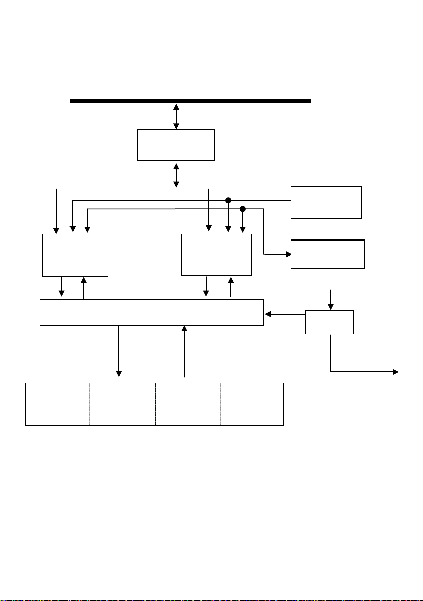
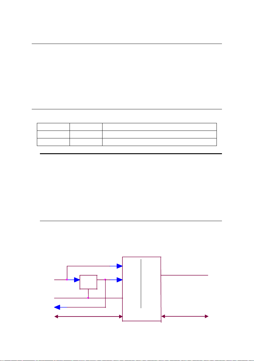
Figure 1.1 shows the function block diagram of PCI-8134/PCI-8134A car d.
PCI-8134/PCI-8134A uses motion ASIC to perform 4-axis motion control.
These ASICs are incorporate Nippon Pulse Motor. The motion control
functions include linear and S-curve acceleration/deceleration, interpolation
between two axes, continuous motion, in positioning and home return are
done by the ASIC. Since these functions needing complex computations are
done internally on the ASIC, the PC’s CPU is free to supervise and perf orm
other tasks.
Motion Creator a Microsoft Windows-based application included with the PCI8134/PCI-8134A card for supporting application development. Motion Creator
is very helpful for debugging a motion control system during the design phase
of a project. The on-screen monitor shows all installed axis information and
I/O signals status of PCI-8134/PCI-8134A cards. In addition to Motion Creator,
both DOS and Windows version function library are included for programmers
using C++ and Visual Basic language. Several sample programs are given to
illustrate how to use the function library.
The following flowcharts show recommending processes for using this manual
to develop an application. Please also refer to the relative chapters for details
of each step.
Introduction • 1
Page 12
CN2
DC/DC
Ext+24V Input
PCL 5023
PCL 5023
Pulser .
y
CN3
CN4
Isolation
ORG
PCI Bus
Ext +5V out
CN1
Pulse I/O
OUT, DIR,
EA, EB, EZ
for axes
X & Y
Mechanical
Interface
+EL, -EL,
+SD,-SD,
PCI Bus
Controller
Servo
Driver
Interface
INP, ALM
ERC
for axes
Z & U
Input: PA,PB
Simultaneousl
General
Purpose
I/O
SVON
RDY
Figure 1.1 Block Diagram of PCI-8134
2 • Introduction
Page 13
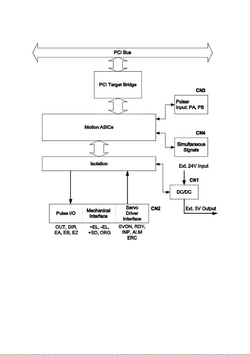
Figure 1.2 Block Diagram of PCI-8134A
Introduction • 3
Page 14

Features
1.1
The following lists summarize the main features of the PCI-8134
motion control system.
• 32-bit PCI-Bus, plug and play.
• 4 axes of step and direction pulse output for controlling stepping or
servomotor.
• Maximum output frequency of 2.4 Mpps
• Pulse output options: OUT/DIR, CE/CCW
• Pulse input options: CW/CCW, AB phase x1, x2, x4
• 2-axis linear interpolation.
• 28-bit up/down counter for incremental encoder feedba ck.
• Home switch, index signal, positive and negative limit switches
interface provided for all axes
• Trapezoidal and S-curve velocity profiles for all modes
• Programmable interrupt sourc es
• Change Speed on the Fly.
• Simultaneous start/stop mot io n on multip le ax es.
• Manual pulser input interface.
• Software supports maximum up to 12 PCI-8134/PCI-8134A cards (48
axes) operation.
• Compact, half size PCB.
• Motion Creator Microsoft Windows based application development
software.
Specifications
1.2
Applicable Motors:
Stepping motors.
AC or DC servomotors with pulse train input servo-drives.
Performance:
Number of controllable axes: 4
Maximum pulse output frequency: 2.4Mpps, linear, trapezoidal or
S-Curve velocity profile drive.
Position pulse setting range: 0~268,435,455 pulses (28-bit).
Ramping-down point setting range: 0 to 16777215
Acceleration / deceleration rate setting range: 1 to 65535(16bit)
Up / down counter counting range: 0~268,435,455 (28-bit.) or –
134,217,728 to +134,217,727
4 • Introduction
Page 15

Pulse rate setting steps: 0 to 2.4Mpps.
I/O Signals:
Input/Output Signals for each axis
All I/O signal are optically isolated with 2500Vrms isolation voltage
Command pulse output pins: OUT and DIR.
Incremental encoder signals input pins: EA and EB.
Encoder index signal input pin: EZ.
Mechanical limit/switch sig nal input pins: ±EL, SD and ORG.
Servomotor interface I/O pins: INP, ALM and ERC.
General purpose digital output pin: SVON.
General purpose digital input pin: RDY.
Pulser signal input pin: PA and PB.
Simultaneous Start/Stop signal I/O pins: STA and STP.
General Specifications
Connectors: 100-pin SCSI-type connector
Operating Temperature: 0° C ~ 50° C
Storage Temperature: -20° C ~ 80° C
Humidity: 5 ~ 85%, non-condensing
Power Consumption:
∗ Slot power supply (input): +5V DC ±5%, 900mA max .
∗ External power supply (input): +24V DC ±5%, 500mA max.
∗ External power supply (output): +5V DC ±5%, 500mA, max.
∗ PCI-8134 Dimensions: 164mm(L) X 98.4mm(W)
∗ PCI-8134A Dimensions: 185mm(L) X 100mm(W)
Introduction • 5
Page 16

Software Support
1.3
1.3.1 Programming Library
Windows® XP/7 DLLs are provided for the PCI-8134 and PCI-8134A. These
function libraries are shipped with the board.
1.3.2 Motion Creator
This Windows-based utility, also bundled with the product, is used to set up
cards, motors, and systems, and can aid in debugging hardware and
software. It allows users to set I/O logic parameters for their own programs.
Compatible Terminal Boards
1.4
ADLINK provides servos & steppers with terminal boards for easy
connection, specifically boards DIN-814M0, DIN-814M-J3A0, DIN-814Y0,
DIN-814P-A40 for connection to dedicated servo drives. Steppers or other
servo brands can be connected with general purpose terminal boards DIN814-GP and DIN-100S0. Com patib le serv os are as foll ows.
Servo Terminal Board
Mitsubishi J2 Super DIN-814M0
Mitsubishi J3A DIN-814M-J3A0
Yaskawa Sigma II DIN-814Y0
Panasonic MINAS A4 DIN-814P-A40
Other Serovs and Steppers DIN-814-GP (specific for cable selection)
DIN-100S0
6 • Introduction
Page 17

2
Installation
This chapter describes how to install the PCI-8134/PCI-8134A, according to
the following procedure.
• Check Package Contents (Section 2.1)
• Check the PCB (Section 2.2)
• Install the hardware (Section 2.3)
• Install the software driver (Section 2.4)
• Acquaint yourself with the I/O signal connections (Chapter 3) and their
operation (Chapter 4)
• Check the connector pin assignments and wiring
Package Contents
2.1
In addition to this User's Guide, the package includes the following items:
• PCI-8134/PCI-8134A 4-Axis Servo / Stepper Motion Control Card
• ADLINK All-in-one Compact Disc
• User’s Guide Manual
If any of these items are missing or damaged, contact the dealer from
whom you purchased the product. Save the shipping materials and carton
in case you want to ship or store the product in the future.
Installation • 7
Page 18
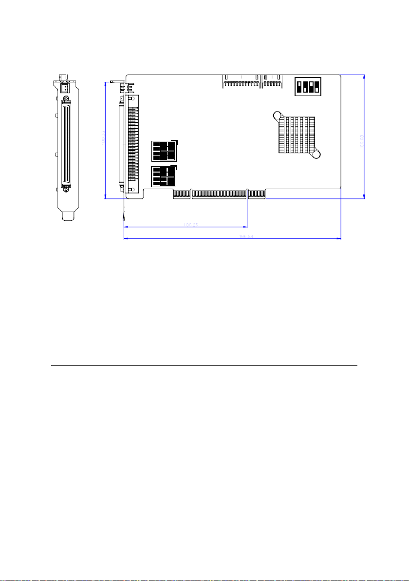
PCI-8134/PCI-8134A Outline Drawing
2.2
Figure 2.1 PCB Layout of the PCI-8134
CN1: External Power Input Connector
CN2: Input / Output Signal Connector
CN3: Manual Pulser Signal Connector
CN4: Simultaneous Start / Stop Connector
8 • Installation
Page 19
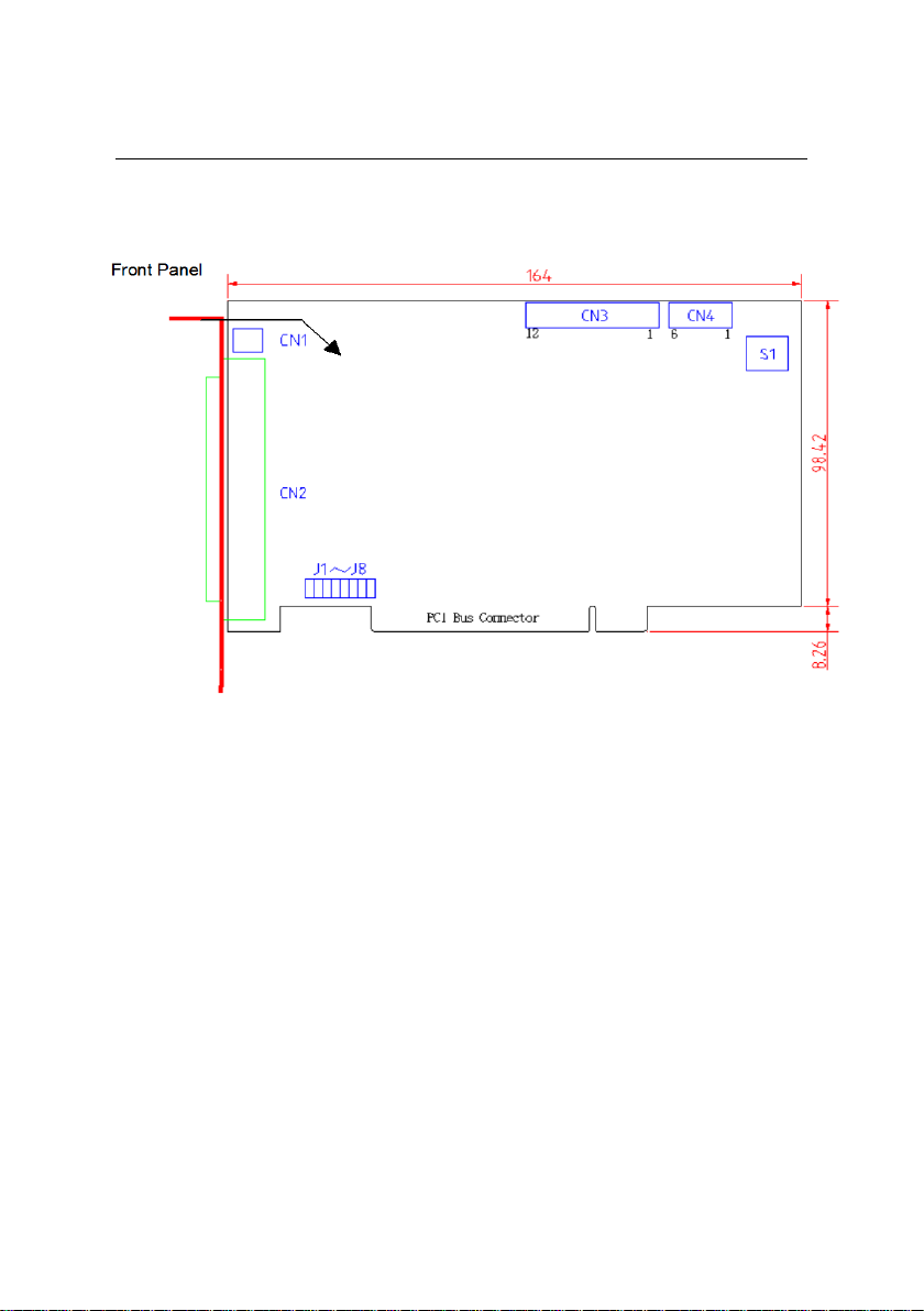
CN4
CN3
CN2
J1
J8
S1
CN1
|
Figure 2.2 PCB Layout of the PCI-8134A
CN1: External Power Input Connector
CN2: Input / Output Signal Connector
CN3: Manual Pulser Signal Connector
CN4: Simultaneous Start / Stop Connector
J1-J8: Pulse output type selection
S1: Polarity of end-limited switch selection
Hardware Installation
2.3
2.3.1 Hardware configuration
The PCI-8134/PCI-8134A has a plug and play PCI controller on board. The
memory usage (I/O port locations) of the PCI card is assigned by system
BIOS. The address assignment is done on a board-by-board basis for all
PCI cards in the system.
2.3.2 PCI slot selection
Your computer will probably have both PCI and ISA slots. Do not force the
PCI card into a PC/AT slot. The PCI-8134/PCI-8134A can be used in any
PCI slot.
Installation • 9
Page 20

2.3.3 Installation Procedures
Read through this manual, and setup the jumper according to your
application
Turn off your computer, Turn off all accessories (printer, modem, monitor,
etc.) connected to computer.
Remove the cover from your computer.
Select a 32-bit PCI expansion slot. PCI slots are short than ISA or EISA
slots and are usually white or ivory.
Before handling the PCI-8134/PCI-8134A, discharge any static buildup on
your body by touching the metal case of the computer. Hold the edge and
do not touch the components.
Position the board into the PCI slot you selected.
Secure the card in place at the rear panel of the system unit using screw
removed from the slot.
2.3.4 Troubleshooting:
If your system won‘t boot or if you experience erratic operation with your
PCI board in place, it’s likely caused by an interrupt conflict (perhaps
because you incorrectly described the ISA setup). In general, the solution,
once you determine it is not a simple oversight, is to consult the BIOS
documentation that comes with your system.
Software Driver Installation
2.4
Please refer to the ADLink All-in-one Compact Disc Manual to install it.
10 • Installation
Page 21
CN1 Pin No
Name
Description
1
EXGND
Grounds of the external power.
2
EX+24V
External power supply of +24V DC
Isolation
DC/DC
+5V
GND
I/O
EX+5V
EXGND
EX+24V
External
Power Supply
(OUTPUT)
Internal
from PCI BUS
(Bus Power)
(External Power)
I/O SIGNALS
Programming Guide Installation
2.5
1) From the ADLINK All-In-One CD Choose Driver Installation>Motion
Control>PCI-8134/PCI-8134A
2) Follow the procedures of the installer.
3) After installation is completed, restart Windows.
Note: Please download the latest software from the ADLINK website if
necessary.
CN1 Pin Assignments: External Power Input
2.6
5%
±
Note:
1. CN1 is a plug-in terminal board with no screw.
2. Be sure to use the external power supply. The +24V DC is used by
external input/output signal circuit. The power circuit is configured
as follows.
3. Wires for connection to CN1.
Solid wire: ϕ 0.32mm to ϕ 0.65mm (AWG28 to AWG22)
Twisted wire: 0.08mm2 to 0.32mm2 (AWG28 to AWG22)
Naked wire length: 10mm standard.
The following diagram shows the external power supply system of the PCI8134/PCI-8134A. The external +24V power must be provided, an on-board
regulator generates +5V for both internal and external usage.
SIGNALS
Power Supply
Installation • 11
Page 22

CN2 Pin Assignments: Main connector
No.
Name
I/O
Function(axis/)
No.
Name
I/O
Function(axis/)
1
EX+5V
O
+5V power supply output
51
EX+5V
O
+5V power supply output
2
EXGND
Ext. power ground
52
EXGND
Ext. power ground
3
OUT1+
O
Pulse signal (+),
53
OUT3+
O
Pulse signal (+),
4
OUT1-
O
Pulse signal (-),
54
OUT3-
O
Pulse signal (-),
5
DIR1+
O
Dir. signal (+),
55
DIR3+
O
Dir. signal (+),
6
DIR1-
O
Dir. signal (-),
56
DIR3-
O
Dir. signal (-),
7
SVON1
O
Multi-purpose signal,
57
SVON3
O
Multi-purpose signal,
8
ERC1
O
Dev. ctr, clr. signal,
58
ERC3
O
Dev. ctr, clr. signal,
9
ALM1
I
Alarm signal,
59
ALM3
I
Alarm signal,
10
INP1 I In-position signal,
60
INP3 I In-position signal,
11
RDY1
I
Multi-purpose signal,
61
RDY3
I
Multi-purpose signal,
12
EXGND
Ext. power ground
62
EXGND
Ext. power ground
13
EA1+ I Encoder A-phase (+),
63
EA3+ I Encoder A-phase (+),
14
EA1- I Encoder A-phase (-),
64
EA3- I Encoder A-phase (-),
16
EB1- I Encoder B-phase (-),
66
EB3- I Encoder B-phase (-),
17
EZ1+ I Encoder Z-phase (+),
67
EZ3+ I Encoder Z-phase (+),
18
EZ1- I Encoder Z-phase (-),
68
EZ3- I Encoder Z-phase (-),
19
EX+5V
O
+5V power supply output
69
EX+5V
O
+5V power supply output
20
EXGND
Ext. power ground
70
EXGND
Ext. power ground
21
OUT2+
O
Pulse signal (+),
71
OUT4+
O
Pulse signal (+),
22
OUT2-
O
Pulse signal (-),
72
OUT4-
O
Pulse signal (-),
23
DIR2+
O
Dir. signal (+),
73
DIR4+
O
Dir. signal (+),
24
DIR2-
O
Dir. signal (-),
74
DIR4-
O
Dir. signal (-),
25
SVON2
O
Multi-purpose signal,
75
SVON4
O
Multi-purpose signal,
26
ERC2
O
Dev. ctr, clr. signal,
76
ERC4
O
Dev. ctr, clr. signal,
27
ALM2
I
Alarm signal,
77
ALM4
I
Alarm signal,
28
INP2 I In-position signal,
78
INP4 I In-position signal,
29
RDY2
I
Multi-purpose signal,
79
RDY4
I
Multi-purpose signal,
30
EXGND
Ext. power ground
80
EXGND
Ext. power ground
31
EA2+ I Encoder A-phase (+),
81
EA4+ I Encoder A-phase (+),
32
EA2- I Encoder A-phase (-),
82
EA4- I Encoder A-phase (-),
34
EB2- I Encoder B-phase (-),
84
EB4- I Encoder B-phase (-),
2.7
The CN2 is the major connector for the motion control I/O signals.
15 EB1+ I Encoder B-phase (+), 65 EB3+ I Encoder B-phase (+),
33 EB2+ I Encoder B-phase (+), 83 EB4+ I Encoder B-phase (+),
12 • Installation
Page 23

36
EZ2- I Encoder Z-phase (-),
86
EZ4- I Encoder Z-phase (-),
38
MEL1
I
End limit signal (-),
88
MEL3
I
End limit signal (-),
40
MSD1
I
Ramp-down signal (-),
90
MSD3
I
Ramp-down signal (-),
42
EXGND
Ext. power ground
92
EXGND
Ext. power ground
44
MEL2
I
End limit signal (-),
94
MEL4
I
End limit signal (-),
46
MSD2
I
Ramp-down signal (-),
96
MSD4
I
Ramp-down signal (-),
48
EXGND
Ext. power ground
98
EXGND
Ext. power ground
50
EXGND
Ext. power ground
100
EX+24V
I
Ext. power supply, +24V
No.
Name
Function(Axis )
1
GND
Bus power ground
2
PB4
Pulser B-phase signal input,
3
PA4
Pulser A-phase signal input,
4
PB3
Pulser B-phase signal input,
5
PA3
Pulser A-phase signal input,
6
+5V
Bus power, +5V
7
GND
Bus power ground
8
PB2
Pulser B-phase signal input,
9
PA2
Pulser A-phase signal input,
10
PB1
Pulser B-phase signal input,
11
PA1
Pulser A-phase signal input,
12
+5V
Bus power, +5V
35 EZ2+ I Encoder Z-phase (+), 85 EZ4+ I Encoder Z-phase (+),
37 PEL1 I End limit signal (+), 87 PEL3 I End limit signal (+),
39 PSD1 I Ramp-down signal (+), 89 PSD3 I Ramp-down signal (+) ,
41 ORG1 I Origin signal, 91 ORG3 I Origin signal,
43 PEL2 I End limit signal (+), 93 PEL4 I End limit signal (+),
45 PSD2 I Ramp-down signal (+), 95 PSD4 I Ramp-down signal (+),
47 ORG2 I Origin signal, 97 ORG4 I Origin signal,
49 EXGND Ext. power ground 99 EX+24V I Ext. power supply, +24V
CN3 Pin Assignments: Manual Pulser Input
2.8
The signals on CN3 is for manual pulser input.
Note: +5V and GND pins are directly given by the PCI-Bus power.
Therefore, these signals are not isolated.
Installation • 13
Page 24
CN4 Pin Assignments: Simultaneous Start/ St op
No.
Name
Function(Axis )
1
GND
Bus power ground
2
STP
Simultaneous stop signal input/out pu t
3
STA
Simultaneous start signal input /out put
4
STP
Simultaneous stop signal input/out pu t
5
STA
Simultaneous start signal input /outpu t
6
+5V
Bus power, +5V
J1
J2
J3
J4
J5
J6
J7
J8
2.9
The signals on CN3 is for simultaneously start/stop signals for multiple axes
and multiple cards.
Note: +5V and GND pins are directly given by the PCI Bus power.
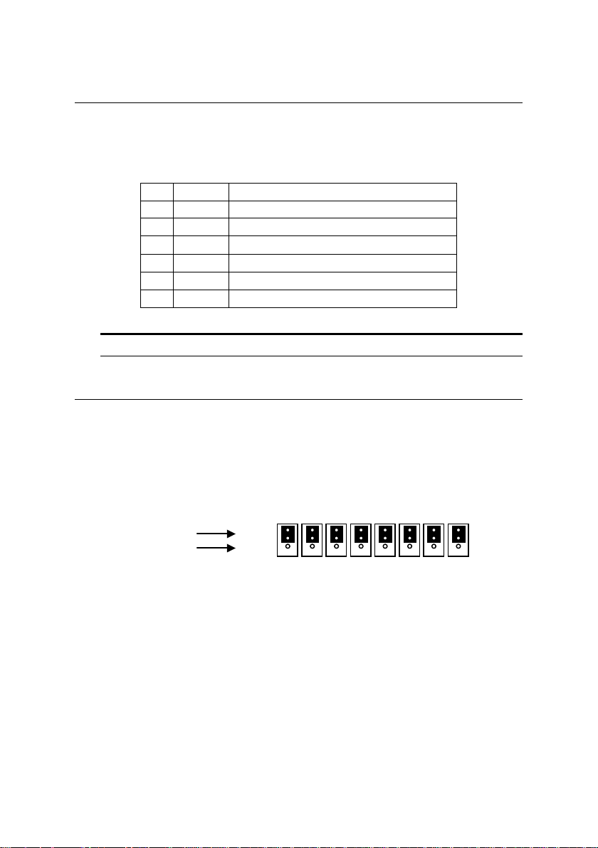
Jumper Setting
2.10
The J1~J8 is used to set the signal type of the pulse output signals (DIR
and OUT). The output signal type could be differential line driver output or
open collector output. Please refer to section 3.1 for details of the jumper
setting. The default setting is the differential line driver mode.
Line Driver
Open Collector
Figure 2.3 Illustration of PCI-8134 jumpers
14 • Installation
1
2
3
Page 25
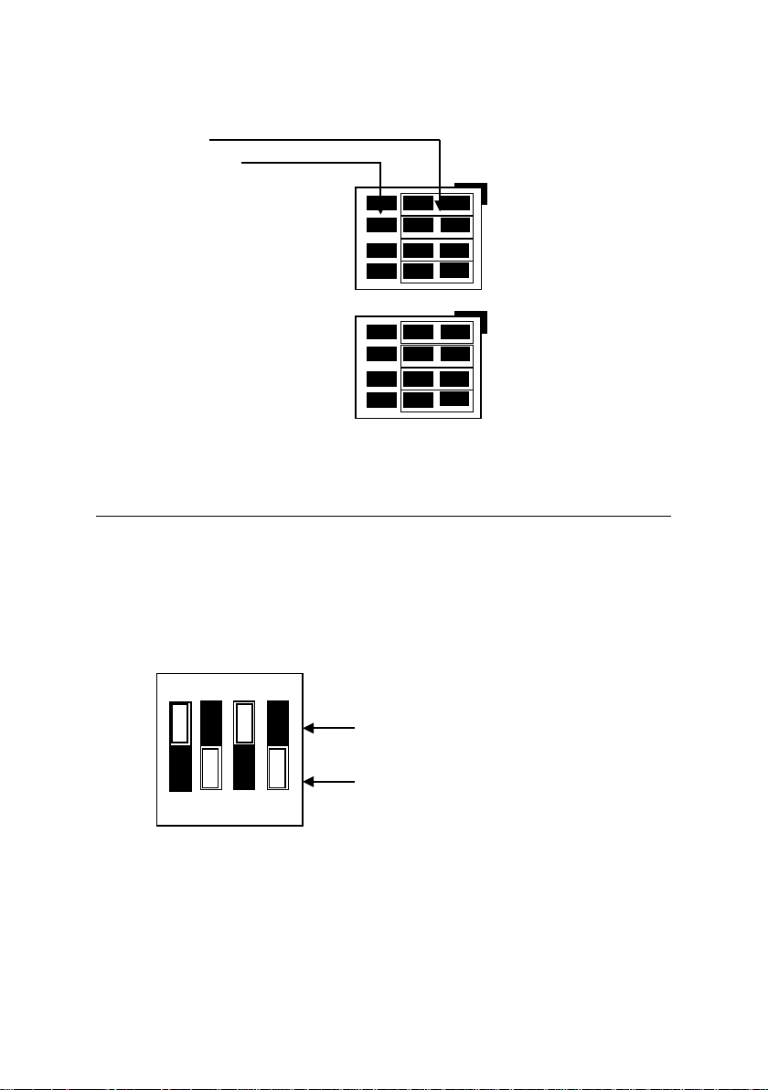
J8
J7
J1
4 3 2 1
ON
Select ‘a’ Contact EL Switch (Normal Open)
3 2 1
Select ‘b’ Contact EL Switch (Normal Close)
Line Driver
Open Collector
J4
J3
J6
J5
J2
Figure 2.4 Illustration of PCI-8134A jumpers
Switch Setting
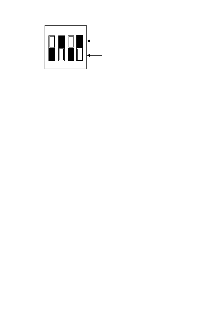
2.11
The switch S1 is used to set the EL limit switch’s type. The default setting
of EL switch type is “normal open” type limit switch (or “A” contact type).
The switch on is to use the “normal closed” type limit switch (or “B” contact
type). The default setting is set as normal open type.
Figure 2.5 Placement of S1 Switch on Board of PCI-8134
Installation • 15
Page 26
1 2 3 4
ON
Select ‘b’ Contact EL Switch (Normal Close)
Select ‘a’ Contact EL Switch (Normal Open)
Figure 2.6 Placement of S1 Switch on Board of PCI-8134A
16 • Installation
Page 27

3
Signal Connections
The signal connections of all the I/O signals are described in this chapter.
Please refer the contents of this chapter before wiring the cable between
the PCI-8134/PCI-8134A and the motor drivers.
This chapter contains the following sections:
Section 3.1 Pulse output signals OUT and DIR
Section 3.2 Encoder feedback signals EA, EB and EZ
Section 3.3 Origin signal ORG
Section 3.4 End-Limit signals PEL and MEL
Section 3.5 Ramping-down signals PSD and MSD
Section 3.6 In-position signal INP
Section 3.7 Alarm signal ALM
Section 3.8 Deviation counter clear signal ERC
Section 3.9 General-purpose signal SVON
Section 3.10 General-purpose signal RDY
Section 3.11 Pulser input signals PA and PB
Section 3.12 Simultaneous start/stop signals STA and STP
Signal Connections • 17
Page 28

Pulse Output Signals OUT and DIR
CN2 Pin No.
Signal Name
Description
Axis #
3
OUT1+
Pulse signals (+)
4
OUT1-
Pulse signals (-)
5
DIR1+
Direction signal(+)
6
DIR1-
Direction signal(-)
21
OUT2+
Pulse signals (+)
22
OUT2-
Pulse signals (-)
23
DIR2+
Direction signal(+)
24
DIR2-
Direction signal(-)
53
OUT3+
Pulse signals (+)
54
OUT3-
Pulse signals (-)
55
DIR3+
Direction signal(+)
56
DIR3-
Direction signal(-)
71
OUT4+
Pulse signals (+)
72
OUT4-
Pulse signals (-)
73
DIR4+
Direction signal(+)
74
DIR4-
Direction signal(-)
3.1
There are 4-axis pulse output signals on PCI-8134/PCI-8134A. For every
axis, two pairs of OUT and DIR signals are used to send the pulse train and
to indicate the direction. The OUT and DIR signals can also be
programmed as CW and CCW signals pair, refer to section 4.1.1 for details
of the logical characteristics of the OUT and DIR signals. In this section,
the electronic characteristics of the OUT and DIR signals are shown. Each
signal consists of a pair of differential signals. For example, the OUT2 is
consisted of OUT2+ and OUT2- signals. The following table shows all the
pulse output signals on CN2.
The output of the OUT or DIR signals can be configured by jumpers as
either the differential line driver or open collector output. You can select the
output mode either by closing breaks between 1 and 2 or 2 and 3 of
jumpers J1~J8 as follows.
18 • Signal Connections
Page 29
differential line driver
between 1 and 2 of
between 2 and 3 of:
OUT1-
J1
J1
DIR1-
J2
J2
OUT2-
J3
J3
DIR2-
J4
J4
OUT3-
J5
J5
DIR3-
J6
J6
OUT4-
J7
J7
DIR4-
J8
J8
VCC
EX+5V
J1~J8
OUT
from Motion ASIC
OUT+, DIR+
OUT-, DIR-
EXGND
R
3
2
2631
CN2
Inside PCI-8134/PCI-8134A
Output
Signal
DIR
For
output, close a break
For open collector
output, close a break
1
default
The
mode.
The following wiring diagram is for the OUT and DIR signals of the 4 axes.
NOTE: If the pulse output is set to the open collector output mode, the
OUT- and DIR- are used to send out signals. Please take care
that the current sink to OUT- and DIR- pins must not exceed 20mA.
The current may provide by the EX+5V power source, however,
please note that the maximum capacity of EX+5V power is 500mA.
setting of OUT and DIR signals are the as differential line driver
Signal Connections • 19
Page 30
Encoder Feedback Signals EA, EB and EZ
CN2 Pin No
Signal Name
Axis #
CN2 Pin No
Signal Name
Axis #
13
EA1+
63
EA3+
14
EA1-
64
EA3-
15
EB1+
65
EB3+
16
EB1-
66
EB3-
31
EA2+
81
EA4+
32
EA2-
82
EA4-
33
EB2+
83
EB4+
34
EB2-
84
EB4-
CN2 Pin No
Signal Name
Axis #
CN2 Pin No
Signal Name
Axis #
17
EZ1+
67
EZ3+
18
EZ1-
68
EZ3-
35
EZ2+
85
EZ4+
36
EZ2-
86
EZ4-
Motion ASIC
EA, EB
EZ
EA+, EB+,
EA-, EBR
Inside PCI-8134/PCI-8134A
3.2
The encoder feedback signals include the EA, EB, and EZ. Every axis has
six pins for three differential pairs of phase-A (EA), phase-B (EB) and index
(EZ) input. The EA and EB are used for position counting; the EZ is used
for zero position index. The relative signal names, pin numbers and the axis
number are shown in the following tables.
The input circuits of the EA, EB, EZ signals are shown as follow s.
EZ+
EZ-
Please note that the voltage across every differential pair of encoder input
signals (EA+, EA-), (EB+, EB-) and (EZ+, EZ-) should be at least 3.5V or
higher. Therefore, you have to take care of the driving capability when
connecting with the encoder feedback or motor driver feedback. The
20 • Signal Connections
Page 31

Encoder Power(VDD)
External Resistor R
+5V
0Ω (None)
+12V
1.8kΩ
+24V
4.3kΩ
If=6mA max.
External Encoder / Driver
PCI-8134/PCI-8134A
A,B phase signals
EA+,EB+,EZ+
EA-, EB-, EZ-
EXGND
GND
differen tial signal pairs will be c onverted t o digital si gnal EA, EB and E Z to
connect to Motion ASIC.
Here are two examples of connecting the input signals with the external
circuits. The input circuits can connect to the encoder or motor driver,
which are equipped with: (1) differential line driver or (2) open collector
output.
Connection to Line Driver Output
To drive the PCI-8134/PCI-8134A encoder input, the driver output must
provide at least 3.5V across the differential pairs with at least 6 mA driving
capability. The ground level of the two sides must be tight together too.
With line driver output
Index signal
Connection to Open Collector Output
To connect with open collector output, an external power supply is
necessary. Some motor drivers also provide the power source. The
connection between PCI-8134/PCI-8134A, encoder, and the power supply
is shown in the following diagram. Please note that the external current
limit resistor R is necessary to protect the PCI-8134/PCI-8134A input ci rc ui t .
The following table lists the suggested resistor value according to the
encoder power supply.
For more detail operation of the encoder feedback signals, please refer to
section 4.4.
Signal Connections • 21
Page 32

CN2 Pin No
Signal Name
Axis #
41
ORG1
47
ORG2
91
ORG3
97
ORG4
EX+24V
I
f
=6mA Max.
Filter
Circuit
Motion ASIC
ORG
Inside PCI-8134/PCI-8134A
CN2
VDD
GND
Motor Encoder / Driver
External Power for
Encoder
PCI-8134/PCI-8134A
A, B phase
signals
EA+, EB+,
EA-, EB-,
R
With Open Collector Output
Origin Signal ORG
3.3
The origin signals (ORG1∼ORG4) are used as input signals for origin of the
mechanism. The following table lists the relative signal name, pin number,
and the axis number.
The input circuits of the ORG signals are shown as following. Usually, a
limit switch is used to indicate the origin of one axis. The specifications of
the limit switches should with contact capacity of +24V, 6mA minim um. An
internal filter circuit is used to filter out the high frequency spike, which may
cause wrong operation.
22 • Signal Connections
← Switch
Page 33

CN2 Pin No
Signal Name
Axis #
CN2 Pin No
Signal Name
Axis #
37
PEL1
87
PEL3
38
MEL1
88
MEL3
43
PEL2
93
PEL4
44
MEL2
94
MEL4
EX+24V
I
f
=6mA Max.
Filter
Circuit
Motion ASIC
PEL
Inside PCI-8134/PCI-8134A
Switch
When the motion controller is operated at the home return mode, the ORG
signal is used to stop the control output signals (OUT and DIR). For the
detail operation of the ORG, please refer to section 4.3.3
End-Limit Signals PEL and MEL
3.4
There are two end-limit signals PEL and MEL for one axis. PEL indicates
end limit signal in plus direction and MEL indicates end limit signal in minus
direction. The relative signal name, pin number and axis number are shown
in the following table.
The signals connection and relative circuit diagram is shown in the following
diagram. The external limit switches featuring a contact capacity of +24V,
6mA minimum. You can use either ‘A-type’ (normal open) contact switch or
‘B-type’ (normal closed) contact switch by setting the DIP switch S1. The
PCI-8134/PCI-8134A is delivered with all bits of S1 set to OFF, refer to
section 2.10. For the details of the EL operation, please refer to section
4.3.2.
MEL
Signal Connections • 23
Page 34

Ramping-down Signals PSD and MSD
CN2 Pin No
Signal Name
Axis #
39
PSD1
40
MSD1
45
PSD2
46
MSD2
89
PSD3
90
MSD3
95
PSD4
96
MSD4
EX+24V
I
f
=6mA Max.
Filter
Circuit
Motion ASIC
PSD
4.7K
Inside PCI-8134/PCI-8134A
CN2
Switch
3.5
There are two ramping-down (Slow−Down) signals PSD and MSD for one
axis. The relative signal name, pin number and axis number are shown in
the following table.
The signals connection and relative circuit diagram is shown in the following
diagram. Usually, limit switches are used to generate the slow−down
signals to make motor operating in a slower speed. For more details of the
SD operation, please refer to section 4.3.1.
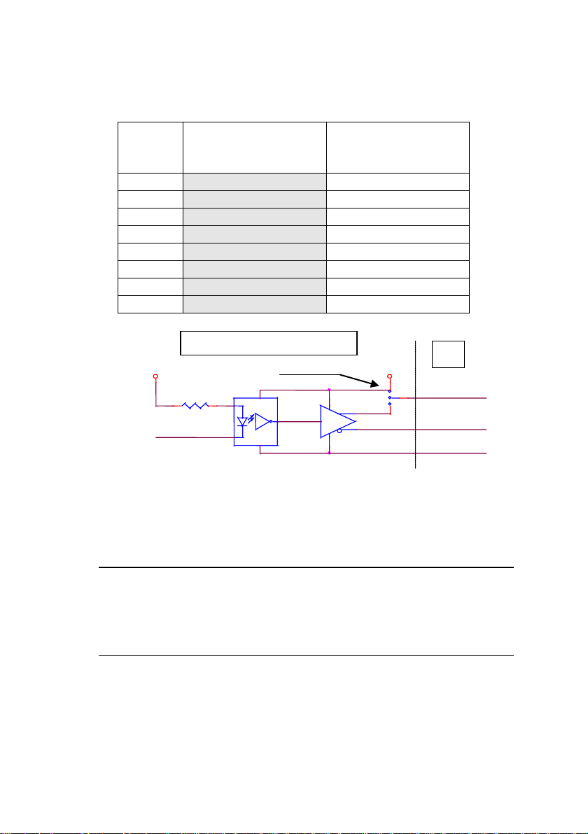
In-position Signal INP
3.6
The in-position signals INP from the servo motor driver indicate the
deviation error is zero, that is the servo position error is zero. The relative
signal name, pin number and axis number are shown in the following table.
24 • Signal Connections
MSD
Page 35

CN2 Pin No
Signal Name
Axis #
10
INP1
28
INP2
60
INP3
78
INP4
CN2 Pin No
Signal Name
Axis # 9 ALM1
27
ALM2
59
ALM3
77
ALM4
EX+5V
If=12mA Max.
Motion ASIC
INP
R
Inside PCI-8134/PCI-8134A
CN2
The input circuit of the INP signals are shown in the following diagram.
I
=5mA Min.
f
The in-position signals are usually from servomotor drivers, which usually
provide open collector output signals. The external circuit must provide at
least 5 mA current sink capability to drive the INP signal active. For more
details of the INP signal operating, please refer to section 4.2.1.
Alarm Signal ALM
3.7
The alarm signal ALM is used to indicate the alarm status from t he servo
driver. The relative signal name, pin number and axis number are shown in
the following table.
The input circuit of alarm circuit is shown in the following diagram. The ALM
signals are usually from servomotor drivers, which usually provide open
Signal Connections • 25
Page 36

collector output signals. The external circuit must provide at least 5 mA
CN2 Pin No
Signal Name
Axis # 8 ERC1
26
ERC2
58
ERC3
76
ERC4
If=12mA Max.
Motion ASIC
Inside PCI-8134/.PCI-8134A
CN2
current sink capability to drive the ALM signal active. For more details of
the ALM operation, please refer to section 4.2.2.
EX+5V
I
=5mA Min.
f
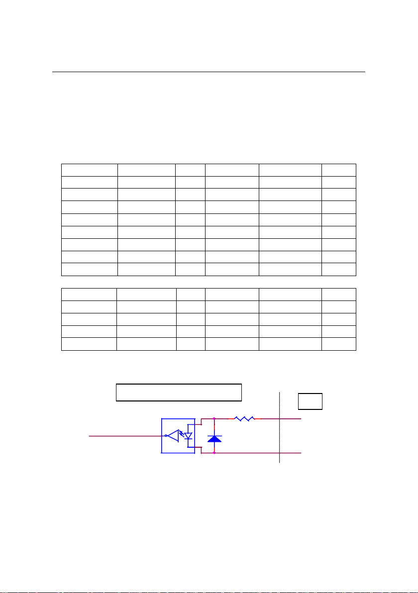
Deviation Counter Clear Signal ERC
3.8
ALM
The deviation counter clear signal (ERC) is active in the following 4
situations:
1. home return is complete;
2. the end-limit switch is act iv e;
3. an alarm signal stops OUT and DIR signals;
4. an emergency stop command is issued by software (operator).
The relative signal name, pin number and axis number are shown in the
following table.
The ERC signal is used to clear the deviation counter of servomotor driver.
The ERC output circuit is in the open collector with maximum 35 V external
26 • Signal Connections
Page 37

CN2 Pin No
Signal Name
Axis # 7 SVON1
25
SVON2
57
SVON3
75
SVON4
35V 50mA Maximum
SVON
Motion ASIC
EXGND
Inside PCI-8134/PCI-8134A
CN2
35V 50mA Maximum
ERC
Motion ASIC
EXGND
Inside PCI-8134/PCI-8134A
power at 50mA driving capability. For more details of the ERC operation,
please refer to section 4.2.3.
General-purpose Signal SVON
3.9
The SVON signals can be used as servomotor-on control or generalpurpose output signals. The relative signal name, pin number and axis
number are shown in the following table.
The output circuit of SVON signal is shown in the following diagram.
General-purpose Signal RDY
3.10
The RDY signals can be used as motor driver ready input or
general−purpose input signals. The relative signal name, pin number and
axis number are shown in the following table.
Signal Connections • 27
Page 38

CN2 Pin No
Signal Name
Axis #
11
RDY1
29
RDY2
61
RDY3
71
RDY4
Pin No
Name
Pin No
Name
2
PA1 8 PA3 3 PB1 9 PB3 4 PA2
10
PA4 5 PB2
11
PB4
If=12mA Max.
Motion ASIC
RDY
Inside PCI-8134/PCI-8134A
CN2
The input circuit of RDY signal is shown in the following diagram
EX+5V
I
=5mA Min.
f
Pulser Input Signals PA and PB
3.11
The PCI-8134/PCI-8134A can accept the input signals from pulser signals
through the following pins of connector CN3. The pulser’s behavior is as an
encoder. The signals are usually used as generate the position information
which guide the motor to follow.
CN3
Signal
Axis #
CN3
Signal
Axis #
PA and PB pins of connector CN3 are directly connected to PA and PB pins
of PCL5023. The interfac circuits are shown as follows.
28 • Signal Connections
Page 39

Motion ASIC
STP
STP, AXIS 3&4
STA, AXIS 3&4
STP, AXIS 1&2
STA, AXIS 1&2
3
4
5
CN4
Inside PCI-8134/PCI-8134A
STA
STP
STA
VCC
PA,PB
Motion ASIC
PA, PB
If the signal voltage of pulser is not +5V or if the pulser is distantly placed, it
is recommended to put a photo coupler or line driver in between. Also, +5V
and GND power lines of CN3 are direct from the PCI bus. Please carefully
use these signals because they are not isolated.
Simultaneously Start/Stop Signals STA and
3.12
STP
The PCI-8134/PCI-8134A provides the STA and STP signals, which enable
simultaneous start/stop of motions on multiple axes. The STA and STP
signals are on the CN4.
In order to implement axes synchronous control between different cards,
both PCI-8134 and PCI-8134A are able to synchronize the axes control
through simultaneous control signals, STA and STP. User is able to connect
each STA and STP signal via CN4 connector as the following illustration.
Also user would use external signals to trigger the simultaneous axes
control.
VCC
4.7K
VCC
4.7K
2
Signal Connections • 29
Page 40

STP
CN4
PCI-8134/PCI-8134A #1
PCI-8134/PCI-8134A #2
PCI-8134/PCI-8134A #3
CN4
CN4
STA
STP
STA
STP
STA
STP
STA
STP
STA
STP
STA
30 • Signal Connections
Page 41

4
Operations
This chapter describes detailed operation of the PCI-8134/PCI-8134A card.
Contents of the following sections are as following.
Section 4.1: The motion control modes
Section 4.2: The motor driver interface (INP, ERC, ALM, SVON, RDY)
Section 4.3: The limit switch interface and I/O status (SD, EL, ORG)
Section 4.4: The encoder feedback signals (EA, EB, EZ)
Section 4.5: Multiple PCI-8134/PCI-8134A cards operation.
Section 4.6: Change Speed on the Fly
Section 4.7: Interrupt Control
Motion Control Modes
4.1
In this section, the pulse output signals’ configurations, and the following
motion control modes are described.
• Constant velocity motion for one axis
• Trapezoidal motion for one axis
• S-Curve profile motion for one axis
• Linear interpolation for two axes
• Home return mode for one axis
• Manual pulser mode for one axis
Operations • 31
Page 42

4.1.1 Pulse Command Output
Mode
Output of OUT pin
Output of DIR pin
CW) direction
CCW) direction
Single pulse output
Pulse signal
Direction signal (level)
OUT
DIR
Positive Command
Negative Command
The PCI-8134/PCI-8134A uses pulse command to control the servo /
stepper motors via the drivers. The pulse command consists of two signals:
OUT and DIR. There are two command types: (1) single pulse output
mode (OUT/DIR); and (2) dual pulse output mode (CW/CCW type pulse
output). The software function: set_pls_outmode() is used to program the
pulse command type. The modes vs. signal type of OUT and DIR pins are
as following table:
Dual pulse output
The interface characteristics of these signals could be differential line driver
or open collector output. Please refer to section 3.1 for the jumper setting
of signal types.
Single Pulse Output Mode (OUT/DIR Mode)
In this mode, the OUT signal is represent the pulse (position or velocity)
command. The numbers of OUT pulse represent the motion command for
relative “distance” or “position”, the frequency of the OUT pulse represents
the command for “speed” or “velocity”. The DIR signal represents direction
command of the positive (+) or negative (-). This mode is the most common
used mode. The following diagram shows the output waveform.
Dual Pulse Output Mode (CW/CCW Mode)
In this mode, the waveform of the OUT and DIR pins represents CW
(clockwise) and CCW (counter clockwise) pulse output respectively. Pulses
output from CW pin makes motor move in positive direction, whereas pulse
output from CCW pin makes motor move in negative direction. The
Pulse signal in plus (or
Pulse signal in min us (or
32 • Operations
Page 43
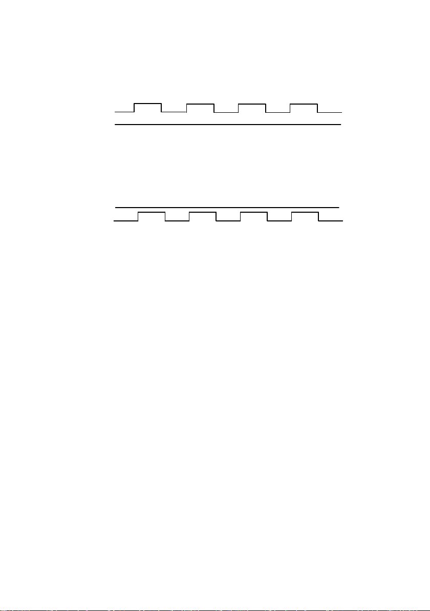
OUT
DIR
Negative Command
OUT
DIR
Positive Command
following diagram shows the output waveform of positive (plus,+) command
and negative (minus,-) com ma nd.
Relative Function:
set_pls_optmode(): Refer to section 6.4
4.1.2 Constant Velocity Motion
This mode is used to operate one axis motor at constant velocity motion.
The output pulse accelerates from a starting velocity (str_vel) to the
specified constant velocity (max_vel). The
accelerate constantly while the
according to S-curve (constant jerk). The pulse output rate will keep at
maximum velocity until another velocity command is set or stop command is
issued. The
v_stop() function is used to decelerate the motion to zero velocity (stop).
The velocity profile is shown as following.
be also be applied to stop outputting command pulses during
(both trapezoidal and S-curve Motion) ,
Mode
operations
Relative Functions:
v_move( ), v_stop( ), sv_move(): Refer to section 6.5
v_change()
.
v_move()
sv_move()
is used to change speed during moving. The
function is to accelerate
Note
Home Mode
function is used to
that v_stop() function can
Preset Mode
Manual Pulser
or
Operations • 33
Page 44

Velocity(pps)
Tacc
Tdec
max_vel
str_vel
Time(second)
v_move()
v_stop()
4.1.3 Trapezoidal Motion
This mode is used to move one axis motor to a specified position (or
distance) with a trapezoidal velocity profile. Single axis is controlled from
point to point. An absolute or relative motion can be performed. In absolute
mode, the target position is assigned. In relative mode, the target
displacement is assigned. In both absolute and relative mode, the
acceleration and the deceleration can be different. The
function is used to check whether the movement is complete.
motion_done()
34 • Operations
Page 45

The following diagram shows the trapezoidal profile. There are 9 relative
functions. In the
start_ta_move()
the unit of pulse. The physical length or angle of one movement is
dependent on the motor driver and the mechanism (includes the motor).
Since absolute move mode needs the information of current actual position,
so “External encoder feedback (EA, EB pins)” must be enabled in
set_cnt_src()
external feedback pulse input must be appropriately set by
set_move_ratio()
functions, the absolute target position must be given in
function. And the ratio between command pulses and
a_move(), ta_move()
function.
and
start_a_move()
,
r_move(), t_move()
In the
the relative displacement must be given in the unit of pulse. Unsymmetrical
trapezoidal velocity profile (Tacc is not equal Tdec) can be specified in
ta_move()
can be specified in
The str_vel and max_vel parameters are given in the unit of pulse per
second (pps). The Tacc and Tdec parameters are given in the unit of
second represent accel./decel. time respectively. You have to know the
physical meaning of “one movement” to calculate the physical value of the
relative velocity or acceleration parameters. The following formula gives the
basic relationship between these parameters.
max_vel = str_vel + accel*Tacc;
str_vel = max_vel + decel *Tdec;
where accel/decel represents the acceleration/deceleration rate in unit of
pps/sec. The area inside the trapezoidal profile represents the moving
distance.
The unit of velocity setting is pulses per second (pps). Usually, the unit of
velocity in the manual of motor or driver is in rounds per minute (rpm). A
simple conversion is necessary to match between these two units. Here we
use a example to illustrate the conversion.
For example:
and
t_move()
a_move()
start_r_move(), start_t_move()
and
functions; where symmetrical profile (Tacc = Tdec)
r_move()
and
functions
functions,
A servo motor with a AB phase encoder is used for a X-Y table. The
resolution of encoder is 2000 counts per phase. The maximum rotating
speed of motor is designed to be 3600 rpm. What is the maximum pulse
command output frequency that you have to set on PCI-8134/PCI-8134A?
Operations • 35
Page 46

Answer:
str_vel
Tacc
Tdec
max_vel
str_vel
Time (second)
max_vel = 3600/60*2000*4
= 48000pps
The reason why *4 is because there are four states per AB phase (See
Figures in Section 4.4).
Velocity (pps)
Usually, the axes need to set the move ratio if their mechanic a l res o lu ti on is
different from the resolution of command pulse. For example, if an
incremental type encoder is mounted on the working table to measure the
actual position of moving part. A servomotor is used to drive the moving
part through a gear mechanism. The gear mechanism is used to convert the
rotating motion of motor into linear motion.(see the following diagram). If the
resolution of motor is 8000 pulses/round. The resolution of gear mechanism
is 100 mm/round.(i.e., part moves 100 mm if motor turns one round). Then
the resolution of command pulse will be 80 pulses/mm. The resolution of
encoder mounting on the table is 200 pulses/mm. Then users have to set
the move ratio as 200/80=2.5 by the function:
set_move_ratio(axis, 2.5);
36 • Operations
Page 47

Motor
Gear
Table
Moving part
Encoder
If this ratio is not set before issuing the start moving command, it will cause
problems when running in “Absolute Mode”. Because the PCI-8134/PCI8134A can’t recognize the actual absolute position during motion.
Relative Functions:
a_move(), r_move(), t_move(), ta_move(), start_a_move(), start_r_move(),
start_t_move(), start_ta_move() Refer to section 6.6.
motion_done(): Refer to section 6.13.
set_cnt_src(): Refer to section 6.4.
set_move_ratio(): Refer to section 6.10.
4.1.4 S-curve Profile Motion
This mode is used to move one axis motor to a specified position (or
distance) with a S-curve velocity profile. S-curve acceleration profiles are
useful for both stepper and servo motors. The smooth transitions between
the start of the acceleration ramp and the transition to the constant velocity
produce less wear and tear than a trapezoidal profile motion. The smoother
performance increases the life of the motors and mechanics of a system.
There are several parameters needed to be set in order to make a S-curve
move. They are:
pos: target position in absolute mode;
dist: moving distance in relative mode;
str_vel : specify the start velocity;
max_vel : specify the maximum velocity;
Tlacc: specify the time for linear acceleration section
(constant acceleration).
Tsacc: specify the time for S-curve acceleration sec tion
Operations • 37
Page 48

(constant jerk).
Tsacc
Tsacc
Tsdec
Tsdec
Tldec: specify the time for linear deceleration section
(constant deceleration).
Tsdec: specify the time for S-curve deceleration section
Tlacc
Tldec
( constant jerk).
Total time of acceleration is: Tlacc+2Tsacc. The following formula gives the
basic relationship between these parameters.
max_vel = str_vel + accel*(Tlacc+Tsacc);
str_vel = max_vel + decel *(Tldec+Tsdec);
accel = Tsacc * jerk1;
decel = Tsdec * jerk2;
where accel/decel represents the acceleration/deceleration rate at linear
accel./decel. section and are in unit of pps/sec. jerk1, jerk2 are in unit of
pps/sec^2. The minimum value for setting time of accel./decel. should be 0.
The S-curve profile motion functions are designed to always produce
smooth motion. If the time for linear/S-Curve acceleration parameters
combined with the final position don’t allow an axis to reach the maximum
38 • Operations
Page 49

Velocity (pps)
velocity( i.e.: the moving distance is too small to reach max_vel), the
maximum velocity is automatically lowered and
smooth accel./decel. is made (see the following Figure). This means that
with moves that don’t reach maximum velocity may cause longer than
expected move times. In such a case, the smaller the moving distance, the
shorter the linear accel./decel. section becomes and the S-curve section is
not reduced unless the linear section is decreased to 0.
Time (sec)
The following two graphs show the results of experiments after executing
the unsymmetrical absolute S-curve motion command. Graph1 is the typical
result. of S-curve velocity profile. Graph2 is obtained when the amount of
command pulses is failed to let the velocity reach the designated maximum
velocity. The PCI-8134/PCI-8134A automatically lower the maximum
velocity thus provide a smooth velocity profile.
Command of Graph1:
start_tas_move(axis, 500000, 100, 1000000, 0.05, 0.05, 0.2, 0.2);
Operations • 39
Page 50

P0
P1
X-Axis
Y-Axis
∆X
∆Y
The total accelerating time = 0.05+2*0.05 = 0.15 (second).
Total decelerating time = 0.2+2*0.2 = 0.6 (second).
Command of Graph2:
start_tas_move(axis, 200000, 100, 1000000, 0.05, 0.05, 0.2, 0.2);
Relative Functions:
s_move(), rs_move(), tas_move(), start_s_move(), start_rs_move(),
start_tas_move() Refer to section 6.7
motion_done(): Refer to section 6.13
4.1.5 Linear Interpolated Motion
In this mode, two axes ( ″X and Y″ or ″Z and U″ axes) is controlled by linear
interpolation or circular interpolation by designating the number of pulses
respectively. ″Interpolation between two axes″ means the two axes start
simultaneously, and reach their ending points at the same time. For
example, in the Figure below, we want to move the axes from P0 to P1, and
hope the two axes start and stop simultaneously at a period of time ∆t. Then
the moving speed along X-axis and Y-axis will be∆X/∆t., ∆Y/∆t. respectively.
40 • Operations
Page 51

The axis with larger numbers of moving pulses is the main axis, and the
other axis is the secondary axis. When both axes are set at the same
amount of pulses, the ‘X’ or ‘Z’ is the main axis. The speed relation
between main and secondary axes is as follows:
Composite Speed = Speed of main axis x
Relative Functions:
move_xy(), move_zu(),Refer to section 6.9
set_move_speed(), set_move_accel(),set_move_ratio(): Refer to section
6.10
4.1.6 Home Return Mode
In this mode, you can let the PCI-8134/PCI-8134A output pulses until the
conditions to complete the home return is satisfied after writing the
home_move()
motion_done()
accompanied with the interrupt function by setting bit 5 of int_factor to 1 in
set_int_factor() function.
Moving direction of motors in this mode is determined by the sign of velocity
parameter in
home can stop OUT and DIR from outputting pulses.
Before writing
set_home_config()
description. There are total three home return modes can be selected by
command. Finish of home return can be checked by
function. Or you can check finish of home return
home_move()
home_move()
function. A
command, configuration must be set by
v_stop()
command during returning
function. . See also Section 4.3.3 for further
Operations • 41
Page 52

setting home_mode parameter in
ORG
EL
PCI-8134 Home Mode 0 + ORG DO not latch
Case 1
Case 2
Case 3
Stand still
Negative
Positive
Case 1
Case 2
Case 3
Stand still
*1
*1
*1 In the case 2 of PCI-8134 Home Mode 0, The axis will stand still and reset counter to 0
and issue home interrupt after user commanded a home move operation.
set_home_config()
meaning of Home_mode will be described as the following:
CAUTION
Due to differences between the motion chipsets of PCI-8134 and PCI-
8134A, behaviour of home mode 0 and 1 will be inconsistent as
performed previously. Please note differences in timing charts of
each home mode for both PCI-8134 and PCI-8134A when user
wants to use PCI-8134A instead of PCI-8134 with same home
function. To ensure the accuracy of home move process, the
motion chipset on PCI-8134A commands backward motion and
stops at the edge of ORG or EZ precisely.
PCI-8134 Home Mode 0 & Home Mode 1
The timing charts of Home Mode 0 and 1 of PCI-8134/PCI-8134A
follow.
function. The
42 • Operations
PCI-8134 Home Mode 0 + ORG do not latch @ 8134.DLL
/8134A.DLL
Page 53

While the motion hits the edge of ORG or EL
set_cnt_src()=0 (internal)
set_cnt_src ()=1 (external)
get_command()
get_position()
get_command()
get_position()
Case 1
Doesn’t change
Reset to 0
Doesn’t change
Reset to 0
Case 2
Doesn’t change
Reset to 0 (stand still)
Doesn’t change
Reset to 0
(stand still)
Case 3
Doesn’t change
Stop at a EL position
Doesn’t change
Stop at a EL
Counter status after Home Move Completed (Motion Done)
set_cnt_src()=0 (internal)
set_cnt_src ()=1 (external)
Interrupt?
get_command()
get_position()
get_command()
get_position()
Case 1 Doesn’t change
Remain 0
Doesn’t change
Stop at a
position
Home Int
Case 3 Doesn’t change
Stop at a EL
position
Doesn’t change
Stop at a EL
position
EL Int
position
deceleration
Case 2 Doesn’t change Reset to 0 Doesn’t ch a n ge Reset to 0
Home Int
• Home point is at the first edge of ORG signal when home move executing.
At left or right side of edge depends on home move direction.
• If axis is not at ORG, the axis will search the edge of ORG as home point.
• In Case 1, the axis is stopped immediately when motion detected the
edge of ORG signal but it might stop at anywhere within the range of
ORG signal that means the home position is inaccurate after home move
function was executed many times.
• The feedback counter of PCI-8134 will be reset to zero while the motion
is hitting the edge of ORG signal.
• In Case 2, the axis will stand still and reset counter to 0 and issue home
interrupt.
• After normal home finished like case 1, users have to copy to position
value to command counter and target position counter at the same time.
Operations • 43
Page 54

ORG
EL
Case 1
Case 2
Case 3
Negative
Case 1
Case 2
Case 3
PCI-8134 Home Mode 0 + ORG latch
Positive
PCI-8134 Home Mode 0 + ORG Latch @ 8134.DLL/8134A.DLL
While the motion hits the edge of ORG or EL
set_cnt_src()=0 (internal)
set_cnt_src ()=1 (external)
get_command()
get_position()
get_command()
get_position()
Case 1
Doesn’t change
Reset to 0
Doesn’t change
Reset to 0
Case 2
Doesn’t change
Stop at a EL position
Doesn’t change
Stop at a EL position
Case 3
Doesn’t change
Stop at a EL position
Doesn’t change
Stop at a EL position
Counter status after Home Move Completed (Motion Done)
set_cnt_src()=0 (internal)
set_cnt_src ()=1 (external)
Interrupt?
get_command()
get_position()
get_command()
get_position()
Case 1
Doesn’t change
Remain 0
Doesn’t change
Stop at a
position
Home Int
Case 2
Doesn’t change
Stop at a EL position
Doesn’t change
Stop at a EL position
EL Int
Case 3
Doesn’t change
Stop at a EL position
Doesn’t change
Stop at a EL position
EL Int
• Home point is at the first edge of ORG signal when home move executing.
At left or right side of edge depends on home move direction.
• If axis is not on ORG, the axis will search the edge of ORG as home point.
• In Case 1, the axis will be stopped immediately when axis detected the
edge of ORG signal but it might stop at anywhere within the range of
ORG signal that means the home position is inaccurate after home move
was executed many times.
44 • Operations
deceleration
Page 55

EZ
EL
PCI-8134 Home Mode 1 + ORG Do not latch
Case 1
Case 2-1
Case 3
Negative
Positive
Case 1
Case 2-2
Case 3
*1 Once user selected “ORG DO NOT LATCH” Mode and pull-up ORG
signal all the time that the PCI-8134 will search first EZ signal edge then stop
immediately once user issued home move command.
ORG
*1
Case 2-2
1st EZ
2
nd
EZ
While the motion hits the edge of EZ or EL
set_cnt_src()=0 (internal)
set_cnt_src ()=1 (external)
get_command()
get_position()
get_command()
get_position()
Case 1
Doesn’t change
Reset to 0
Doesn’t change
Reset to 0
Case 2-1
Doesn’t change
Reset to 0
Doesn’t change
Reset to 0
Case 2-2
Doesn’t change
Stop at a EL position
Doesn’t change
Stop at a EL position
Case 3
Doesn’t change
Stop at a EL position
Doesn’t change
Stop at a EL position
• The feedback counter of PCI-8134 will be reset to zero while the motion
is hitting the edge of ORG signal.
• In Case 2 & 3, the axis will hit and then stop at the edge of EL signal
anyway because the first edge of ORG signal locates behind the start
point of axis that means the axis won’t detect the edge of ORG signal
anymore.
PCI-8134 Home Mode 1 + ORG do not latch @ 8134A.DLL
/8134.DLL
Operations • 45
Page 56

Counter status after Home Move Completed (Motion Done)
Set_cnt_src()=0 (i nternal)
set_cnt_src ()=1 (external)
Get_command()
get_position()
get_command()
get_position()
position
Case 2-1
Doesn’t change
Remain 0
Doesn’t change
Stop at a deceleration
position
Home Int
Case 2-2
Doesn’t change
Stop at a EL
position
Doesn’t change
Stop at a EL position
EL Int
Case 3
Doesn’t change
Stop at a EL
position
Doesn’t change
Stop at a EL position
EL Int
Interrupt?
Case 1 Doesn’t change Remain 0 Doesn’t change Stop at a deceleration
• In Case 1, the axis will be stopped immediately when axis detected the
edge of ORG signal but it might stop at anywhere within the range of
ORG signal that means the home position is inaccurate after home move
was executed many times.
• The feedback counter of PCI-8134 will be reset to zero while the motion
is hitting the edge of ORG signal.
• As Do Not Latch mode, the axis will start searching EZ signal after the
ORG signal was detected within 5 clock periods.
• In Case 2-2 & 3, the axis will hit and then stop at the edge of EL signal
anyway because the edge of EZ signal locates behind the start point of
Home Move that the axis won’t detect the edge of EZ signal anymore.
• In Case 2-1, if there are two or more EZ signals in the system, the axis
will search next EZ signal because the ORG signal was turned ON
continuously.
Home Int
• After normal home finished like case 1, users have to copy to position
value to command counter and target position counter at the same time.
46 • Operations
Page 57

PCI-8134 Home Mode 1 + ORG latch
ORG
EL
Case 1
Case 2
Negative
Positive
Case 1
EZ
ORG latch
Case 3
Case 2
Case 3
While the motion hits the edge of EZ or EL
set_cnt_src()=0 (internal)
set_cnt_src ()=1 (external)
get_command()
get_position()
get_command()
get_position()
Case 1
Doesn’t change
Reset to 0
Doesn’t change
Reset to 0
Case 2
Doesn’t change
Stop at a EL position
Doesn’t change
Stop at a EL position
Case 3
Doesn’t change
Stop at a EL position
Doesn’t change
Stop at a EL position
Counter status after Home Move Completed (Motion Done)
Set_cnt_src()=0 (i nternal)
set_cnt_src ()=1 (external)
Interrupt?
Case 1
Doesn’t change
Remain 0
Doesn’t change
Stop at a
position
Home Int
Case 2
Doesn’t change
Stop at a EL position
Doesn’t change
Stop at a EL position
EL Int
Case 3
Doesn’t change
Stop at a EL position
Doesn’t change
Stop at a EL position
EL Int
PCI-8134 Home Mode 1 + ORG latch @ 8134.DLL/8134A.DLL
Get_command() get_position() get_command() get_position()
• In Case 1, the axis will be stopped immediately when axis detected the
edge of ORG signal but it might stop at anywhere within the range of
ORG signal that means the home position is inaccurate after home move
was executed many times.
• The feedback counter of PCI-8134 will be reset to zero while the motion
is hitting the edge of ORG signal.
deceleration
Operations • 47
Page 58

• As Do Not Latch mode, the axis will start searching EZ signal afte r the
ORG
EL
Case 1
Case 2
Case 3
Negative
Case 1
Case 2
Case 3
PCI-8134A Home Mode 0
Positive
Stand still
*1
*1 In the case 2 of PCI-8134A Home Mode 0, The axis will stand still and reset counter to 0
But won’t issue home interrupt after user issued home move command.
Stand still
*1
ORG signal was detected within 5 clock periods.
• In Case 2 & 3, the axis will hit and then stop at the edge of EL signal
anyway because the edge of EZ signal locates behind the start point of
Home Move that the axis won’t detect the edge of EZ signal anymore.
• In Case 2 & 3, if there are two or more EZ signals in the system, the axis
never stop if the axis starts from first EZ signal because there is no ORG
signal was triggered prior to EZ searching.
• After normal home finished like case 1, users have to copy to position
value to command counter and target position counter at the same time.
PCI-8134A Home Mode 0 & Home Mode 1
The timing charts of Home Mode 0 and 1 of PCI-8134A follow.
PCI-8134A Home Mode 0 @ 8134.DLL /81 34A. DLL /8134A.DLL
48 • Operations
Page 59

While the motion hits the edge of ORG or EL
Set_cnt_src()=0 (i nternal)
set_cnt_src ()=1 (external)
Get_command(
)
get_position()
get_command()
get_position()
Case 1
Doesn’t change
Reset to 0
Doesn’t change
Reset to 0
Case 2
Doesn’t change
Stand Still
Doesn’t change
Stand Still
Case 3
Doesn’t change
Stop at a EL position
Doesn’t change
Stop at a EL position
Counter status after Home Move Completed (Motion Done)
set_cnt_src()=0 (internal)
set_cnt_src ()=1 (external)
Interrupt?
Case 1 Doesn’t change
Remain 0
Doesn’t change
Remain 0
Home Int
Case 2 Doesn’t change
Reset to 0
Doesn’t change
Reset to 0
No Int
position
position
get_command() get_position() get_command() get_position
Case 3 Doesn’t change Stop at a EL
Doesn’t change Stop at a EL
()
EL Int
• Home point is at the first edge of ORG signal when home move executing.
At left or right side of edge depends on home move direction.
• If axis is not at ORG, the axis will search the edge of ORG as home point.
• In Case 1, the axis will slow down and reverse to search the ORG edge
again and then stop at the edge of ORG signal precisely.
• The feedback counter of PCI-8134A will be reset to zero while the motion
is hitting the edge of ORG signal.
• In Case 2, the axis will be standstill and reset counter to 0 but won’t issue
home interrupt.
• After normal home finished like case 1, users have to copy to position
value to command counter and target position counter at the same time.
Operations • 49
Page 60

EZ
EL
PCI-8134A Home Mode 1
Case 1
Case 2
Case 3
Negative
Positive
Case 1
Case 2
Case 3
ORG
While the motion hits the edge of EZ or EL
set_cnt_src()=0 (internal)
set_cnt_src ()=1 (external)
get_command()
get_position()
get_command()
get_position()
Case 1
Doesn’t change
Reset to 0
Doesn’t change
Reset to 0
Case 3
Doesn’t change
Stop at a EL position
Doesn’t change
Stop at a EL position
Counter status after Home Move Completed (Motion Done)
set_cnt_src()=0 (internal)
set_cnt_src ()=1 (external)
Interrupt?
get_command()
get_position()
get_command()
get_position()
Case 1
Doesn’t change
Remain 0
Doesn’t change
Remain 0
Home Int
Case 3
Doesn’t change
Stop at a EL position
Doesn’t change
Stop at a EL
position
EL Int
PCI-8134A Home Mode 1 @ 8134.DLL /81 34A .DLL
DLL version: 110420, Driver version: 101109
Case 2
Doesn’t change Stop at a EL position Doesn’t change Stop at a EL position
Case 2 Doesn’t change Stop at a EL position D oe sn’t change Stop at a EL
• In Case 1, the axis will search the edge of EZ signal after the ORG signal
and then stop at EZ edge precisely.
50 • Operations
position
EL Int
Page 61

time
mvel
svel
Velocity
accel
ORG
• The feedback counter of PCI-8134 will be reset to zero while the motion
is hitting the edge of EZ or EL signal.
• In Case 2 & 3, the axis will hit and then stop at the edge of EL signal
anyway because the edge of EZ signal locates behind the start point of
Home Move that the axis won’t detect the edge of EZ signal anymore.
• After normal home finished like case 1, users have to copy to position
value to command counter and target position counter at the same time.
(3) Home_mode=2: both ORG and index signal are useful. The ORG
signal let s th e PCI-8134/PCI-8134A decelerate to starting velocity
and then EZ signal stops OUT and DIR pins from outputting
pulses to complete the home return.
EZ
Note: If the starting velocity is zero, the axis will work properly in home
Relative Function:
set_home_config(), home_move(), v_stop(): Refer to section 6.11
mode 2.
Operations • 51
Page 62

4.1.7 Manual Pulser Mode
For manual operation of a device, you may use a manual pulser such as a
rotary encoder. The PCI-8134/PCI-8134A can input signals from the pulser
and output corresponding pulses from the OUT and DIR pins, thereby
allowing you to simplify the external circuit and control the present position
of axis. This mode is effective between a
written and a
The PCI-8134/PCI-8134A receives plus and minus pulses (CW/CCW) or 90
degrees phase difference signals(AB phase) from the pulser at PA and PB
pins. The 90°phase difference signals can be input through multiplication
by 1, 2 or 4. If the AB pahse input mode is selected, the PA and PB signals
should be with 90° phase shifted, and the position counting is increasing
when the PA signal is leasding the PB signal by 90° phase.
Also, one pulser may be used for ‘X’ and ‘Y’ axes while internally
distributing the signals appropriately to two axes. To set the input signal
modes of pulser, use
manu_move()
command in order to end this function and begins to operate at another
mode.
The error input of PA and PB can be used to generate IRQ. The following
two situations will be considered as error input of PA and PB signals. (1)
The PA and PB signals are changing simultaneously. (2) The input pulser
frequency is higher than the maximum output frequency 2.4M pps. Set bit
14 of INT factor will enable the IRQ when error happen.
v_stop()
to begin manual operation function. User must write
command.
set_manu_iptmode()
manu_move()
function. Then write
command is
v_stop()
Maximum moving velocity in this mode can be limited by setting max_vel
parameter in
Relative Function:
52 • Operations
manu_move()
set_manu_iptmode(), manu_move(), v_stop(): Refer to section 6.12
function.
Page 63

Motor Drive Interfac e
4.2
The PCI-8134/PCI-8134A provides the INP, ERC and ALM signals for
servomotor driver’s control interface. The INP and ALM are used for
feedback the servo driver’s status. The ERC is used to reset the servo
driver’s deviation counter unde r specia l cond itio ns.
4.2.1 INP
Usually, servomotor driver with pulse train input has a deviation (position
error) counter to detect the deviation between the input pulse command and
feedback counter. The driver controls the motion of servomotor to minimize
the deviation until it becomes 0. Theoretically, the servomotor operates
with some time delay from command pulses. Accordingly, when the pulse
generator stops outputting pulses, the servomotor does not stop but keep
running until the deviation counter become zero. At this moment, the servo
driver sends out the in-position signal (INP) to the pulse generator to
indicate the motor stops running.
Usually, the PCI-8134/PCI-8134A stops outputting pulses upon completion
of outputting designated pulses. But by setting inp_enable parameter in
set_inp_logic() function, you can delay the completion of operation to the
time when the INP signal is turned on. Status of
signal are also delayed. That is, when performing under position control
mode, the completion of
start_s_move()
… functions are delayed until INP signal is turned ON.
start_a_move(), start_r_move()
motion_done()
and INT
,
However, EL or ALM signal or the completion of home return does not
cause the INP signal to delay the timing of completion. The INP signal may
be a pulse signal, of which the shortest width is 5 micro seconds.
The in-position function can be enable or disable. The input logic polarity
isalso programmable by software function:
status can be monitored by software function:
set_inp_logic()
get_io_status()
. The signal
.
4.2.2 ALM
The ALM pin receives the alarm signal output from the servo driver. The
signal im mediately stops the PCI-8134/PCI-8134A from generating pulses
or stops it after deceleration. If the ALM signal is in the ON status at the
start, the PCI-8134/PCI-8134A outputs the INT signal without generating
Operations • 53
Page 64

any command pulse. The ALM signal may be a pulse signal, of which the
ERC Output
Approximate 10ms
shortest width is a time length of 5 micro seconds.
You can change the input logic by set_alm_logic() function. Whether or not
the PCI-8134/PCI-8134A is generating pulses, the ALM signal lets it output
the INT signal.. The ALM status can be monitored by software function:
get_io_status(). The ALM signal can generate IRQ by setting the bit 2 of
INT. factor in software function:
set_int_factor().
4.2.3 ERC
The deviation counter clear signal is inserted in the following 4 situations:
(1) home return is complete;
(2) the end-limit switch is active;
(3) an alarm signal stops OUT and DIR signals;
(4) an emergency stop command is issued by software operator.
Since the servomotor operates with some delay from pulse generated from
the PCI-8134/PCI-8134A, it keeps operating by responding to the position
error rem ainin g in the de viat ion counter of the driver if the ±EL signal or the
completion of home return stops the PCL5023 from outputting pulses. The
ERC signal allows you to immediately stop the servomotor by resetting the
deviation counter to zero. The ERC signal is output as an one-shot sign al.
The pulsewidth is a time length of 10ms. The ERC signal will automatically
output when ±EL signals, ALM signal is turned on to immediately stop the
servomotor. User can set the ERC pin output enable/disable by
set_erc_enable() function. ERC pin output is set output enabled when
initializing.
54 • Operations
OFF
ON
Page 65

CAUTION
Due to differences between the motion chipsets on the PCI-8134 and PCI8134A, ERC output pulse width with the PCI-8134A may be less than
originally output by the PCI-8134.
The Limit Switch Interface and I/O Status
4.3
In this section, the following I/O signals’ operations are described.
• SD: Ramping Down sensor
• ±EL: En d-limit sensor
• ORG: Origin position
• SVON a nd RDY
I/O status readback
In any operation mode, if an ±EL signal is active during moving condition, it
will cause PCI-8134/PCI-8134A to stop output pulses automatically. If an
SD signal is active during moving condition, it will cause PCI-8134/PCI8134A to decelerate.
4.3.1 SD
The ramping-down signals are used to slow-down the control output signals
(OUT and DIR) when it is active. The signals are very useful to protect the
mechanism moving under high speed toward the mechanism limit. PSD
indicates ramping-sown signal in plus (+) direction and MSD indicates
ramping-down signal in minus (-) direction.
During varied speed operation in the home return mode or continuous
operation mode, the ramping-down signal in the moving direction lets the
output control signals (OUT and DIR) ramp down to the pre-setting starting
velocity.
The ramping-down function can be enable or disable by software function:
set_sd_logic()
input mode can also be set by this function. The signals status can be
monitored by
. The input logic polarity, level operation mode, or latched
get_io_status()
.
4.3.2 EL
Operations • 55
Page 66

The end-limit signals are used to stop the control output signals (OUT and
DIR) when the end-limit is active. PEL signal indicates end-limit in positive
(plus) direction. MEL signal indicates end-limit in negative (minus) direction.
When the output pulse signals (OUT and DIR) are toward positive direction,
the pulse train will be immediately stopped when the PEL signal is inserted,
while the MEL signal is meaningless in this case, and vise versa. When the
PEL is inserted and the output pulse is fully stop, only the negative (minus)
direction output pulse can be generated for moving the motor to negative
(minus) direction.
The end-limit signals can be used to generate the IRQ by setting the bit 0 of
INT. factor in software function:
set_int_factor()
.
56 • Operations
Page 67

You can use either 'a' contact switch or 'b' contact switch by setting the dip
switch S1. The PCI-8134/PCI-8134A is delivered from the factory with all
bits of S1 set to OFF.
The signal status can be monitored by software functi on:
get_io_status().
4.3.3 ORG
When the mo tion controller is operated at the home return mode, the ORG
signal is used to stop the control output signals (OUT and DIR).
There are three home return modes, you can select one of them by setting
“home_mode” argument in software function: set_home_config(). Note that
if home_mode=1 or 2, the ORG signal must be ON or latched during the EZ
signal is inserted (EZ=0). The logic polarity of the ORG signal, level input or
latched input mode are selectable by software function:
After setting the configuration of home return mode by
a home_move() command can perform the home return function.
The ORG signal can also generate IRQ signal by setting the bit 5 of
interrupt reason register (or INT. factor) in software function:
set_int_factor()
.
set_home_config()
set_home_config()
.
,
4.3.4 SVON and RDY
The SVON signals are controlled by software function: _
The function set the logic of SVON signal. The signal status of SVON pins
can be monitored by software function:
RDY pins are dedicated for digital input use The status of this signal can be
monitored by software function get_io_status(). The RDY signal can also
generate IRQ signal by setting the bit 23 of INT. factor in software function:
set_int_factor(). Note that interrupt is generated when RDY signal from
high to low.
get_io_status()
8134_Set_SVON()
.
.
The PCI-8134A supports neither RDY signal connection nor interrupt
function.
Operations • 57
Page 68

The Encoder Feedback Signals (EA, EB, EZ)
4.4
The PCI-8134/PCI-8134A has a 28-bits binary up/down counter for
managing the present position for each axis. The counter counts signals
input from EA and EB pins.
It can accept 2 kinds of pulse input: (1). plus and minus pulses
input(CW/CCW mode); (2). 90° phase difference signals (AB phase mode).
90° phase difference signals may be selected to be multiplied by a factor of
1,2 or 4. 4x AB phase mode is the most commonly used for incremental
encoder input. For example, if a rotary encoder has 2000 pulses per phase
(A or B phase), then the value read from the counter will be 8000 pulses per
turn or –8000 pulses per turn depends on its turning direction. These input
modes can be selected by set_pls_iptmode() function.
To enable the counters counting pulses input from (EA, EB) pins, set
“cnt_src” parameter of softwar e functi on set_cnt_src() to 1.
Plus and Minus Pulses Input Mode(CW/CCW Mode)
The pattern of pulses in this mode is the same as Dual Pulse Output Mode
in Pulse Command Output section, expect that the input pins are EA and
EB.
In this mode, pulse from EA causes the counter to count up, whereas EB
caused the counter to count down.
90° phase difference signals Input Mode(AB phase Mode)
In this mode, the EA signal is 90° phase leading or lagging in comparison
with EB signal. Where “lead” or “lag’ of phase difference between two
signals is caused by the turning direction of motors. The up/down counter
counts up when the phase of EA signal leads the phase of EB signal.
The following diagram shows the waveform.
58 • Operations
Page 69

EA
EB
Negative Direction
EA
EB
Positive Direction
The encoder error interrupt is provided to detect abnormal situation.
Simultaneously changing of EA and EB signals will cause an encoder error.
If bit #14 of the interrupt factor register (INT factor) is set as 1, the IRQ will
be generated when detect encoder error during operation.
The index inputs (EZ) signals of the encoders are used as the “ZERO”
index. This signal is common on most of the rotational motors. EZ can be
used to define the absolute position of the mechanism. The input logic
polarity of the EZ signals is programmable by software function
set_home_config(). The EZ signals status of the four axis can be
monitored by get_io_status().
Relative Function:
set_cnt_src(), set_pls_iptmode(): Refer to section 6.4
Multiple PCI-8134/PCI-8134A Cards Operation
4.5
The software function library support maximum up to 12 PCI-8134/PCI8134A Cards that means maximum up to 48 axes of motors can be
controlled. Since PCI-8134/PCI-8134A has the characteristic of Plug-andPlay, users do not have to care about setting the Based address and IRQ
level of cards. They are automatically assigned by the BIOS of system
when booting up. Users can utilize Motion Creator to check if the plugged
PCI-8134/PCI-8134A cards are successfully installed and see the Base
address and IRQ level assigned by BIOS.
One thing needed to be noticed by users is to identify the card number of
PCI-8134/PCI-8134A when multiple cards are applied. The card number of
one PCI-8134/PCI-8134A depends on the locations on the PCI slots. They
Operations • 59
Page 70

are numbered either from left to right or right to left on the PCI slots. These
Card No.
1 0 1 2 3
2 4 5 6 7
3 8 9
10
11
card numbers will affect the corresponding axis number on the cards. And
the axis number is the first argument for most functions called in the library.
So it is important to identify the axis number before writing application
programs. For example, if 3 PCI-8134/PCI-8134A cards are plugged in the
PCI slots. Then the corresponding axis number on each card will be:
Axis No.
If we want to accelerate Axis 3 of Card2 from 0 to 10000pps in 0.5sec for
Constant Velocity Mode operation. The axis number should be 6. The code
on the program will be:
v_move(6, 0, 10000, 0.5);
To determine the right card number, Try and Error may be necessary before
application. Motion Creator can be utilized to minimize the search time.
The newest DLL supports the combination of both PCI-8134 and PCI8134A in one system.
Change Speed on the Fly
4.6
You can change the velocity profile of command pulse ouput during
operation by v_change() function. This function changes the maximum
velocity setting during operation. However, if you operate under “Preset
Mode” (like start_a_move(),…), you are not allowed to change the
acceleration parameter during operation because the deceleration point is
pre-determined. But changing the acceleration parameter when operating
under “Constant Velocity Mode” is valid. Changing speed pattern on the fly
is valid no matter what you choose “Trapezoidal Velocity Profile” or “S-curve
Velocity Profile”. Here we use an example of Trapezoidal velocity profile to
illustarte this function.
Axis 1 Axis 2 Axis 3 Axis 4
Example: There are 3 speed change sensor during an absolute move for
200000 pulses. Initial maximum speed is 10000pps. Change to 25000pps if
60 • Operations
Page 71

Motor
Sensor 2
Sensor 3
Pos=200000
Moving part
Sensor 1
Sensor 1 is touched. Change to 50000pps if Sensor 2 is touched. Change
to 100000pps if Sensor 3 is touched. Then the code for this application and
the resulting velocity profiles are shown below.
#include “pci_8134.h”
start_a_move(axis, 200000 .0, 1000, 10000, 0.02);
while(!motion_done(axis))
{
// Get Sensor’s information from other I/O card
if((Sensor1==High) && (Sensor2==Low) && (Sensor3 == Low))
v_change(axis, 25000, 0.02);
else if((Sensor1==Low) && (Sensor2==High) && (Sensor3 == Low))
v_change(axis, 50000, 0.02);
else if((Sensor1==Low) && (Sensor2==Low) && (Sensor3 == High))
v_change(axis, 100000, 0.02);
}
Where the informations of three sensors are acquired from other I/O card.
And the resulting velocity profile from experiment is shown below.
Operations • 61
Page 72

Relative Function:
v_change(): Refer to section 6.5
Interrupt Control
4.7
The PCI-8134/PCI-8134A motion controller can generate INT signal to host
PC according to 13 types of factors, refer to
more details.. The INT signal is output when one or more interrupt factors
occur on either axis. To judge on which axis the interrupt factors occur, use
get_int_axis()
get_int_status()
function. The interrupt status is not closed until
function is performed.
set_int_factor()
function for
62 • Operations
Page 73

5
Motion Creator
After installing all the hardware properly according to Chapter 2, 3,
configuring cards and checkout are required before running. This chapter
gives guidelines for establishing a control system and manually exercising
the PCI-8134/PCI-8134A cards to verify correct operation. Motion Creator
provides a simple yet powerful means to setup, configure, test and debug
motion control system that uses PCI-8134/PCI-8134A cards.
Note that Motion Creator is available only for Windows XP/7 with the screen
resolution higher than 800x600 environment and can not run on DOS
system.
Motion Creator • 63
Page 74

Main Menu
5.1
Main Menu will appear when executing Motion Creator. Figure 5.1 shows
the Main Menu.
Figure 5.1 Main Menu of Motion Creator
From main menu window all PCI-8134/PCI-8134A cards and their axes and
the corresponding status can be viewed. First of all, check if all the PCI8134/PCI-8134A cards which are plugged in the PCI-Bus can be viewed on
“Select Card” column. Next select the card and axis you want to configure
and operate. Since there are totally four axes on a card, the axis number of
first axis on n-the card will be numbered as 4*(n-1). Base address and IRQ
level of the card are also shown on this window.
64 • Motion Creator
Page 75

Axis Configuration Window
5.2
Press the “Config Axis” button on the Main Menu will enter the Axis
Configuration window. Figure 5.2 shows the window.
Figure 5.2 Axis Configuration Window
the Axis Configuration window includes the following setting items which
cover most I/O signals of PCI-8134/PCI-8134A cards and part of the
interrupt factors.
• Pulse I/O Mode:
Related functions:
∗ set_pls_outmode() for “Pulse Output Mode” property.
∗ set_cnt_src() for “Pulse Input Active” property.
Motion Creator • 65
Page 76

∗ set_pls_iptmode() for “Pulse Input Mode” property.
66 • Motion Creator
Page 77

• Mechanical Signal:
Related functions:
∗ set_home_config() for “Home Signal” and “Index Signal” property.
∗ set_sd_logic() for “Slow Down Point Signal” property.
• Servo Motor Signal:
Related functions:
∗ set_alm_logic() for “Alarm Signal” property.
∗ set_inp_logic() for “INP” property.
• Manual Pulser Input Mode:
Related functions:
∗ set_manu_iptmode() for “Manual Pulser Input Mode” property.
• Interrupt Factor:
Related functions:
∗ set_int_factor() for “INT Factor” property.
• Home Mode:
Related functions:
∗ set_home_config() for “Home Mode” property.
The details of each section are shown at its related functions.
After selecting all the items you want to configure, user can choose to push
the “Save Configurations “ button on the right bottom side. If you push this
button, all the configurations you select for system integration will be saved
to a file called “8134.cfg”. This file is very helpful when user is developing
their own application programs. The following example illustrate how to
make use of this function. This example program is shown in C language
form.
Main ()
{
_8134_intial ();
8134A cards
_8134_Set_Config ();
according
:
:
}
//
Configure PCI-8134/PCI-8134A cards
//
Initialize the PCI-8134/PCI-
//
to 8134.cfg
Motion Creator • 67
Page 78

Where _8134_initial () and _8134_Set_Config () can be called from the
function library we provide. _8134_initial () should be the first fu nc t io n c al led
within main {} function. It will check all the PCI-8134/PCI-8134A existed and
give the card a base address and IRQ level. _8134_Set_Config () will
configure the PCI-8134/PCI-8134A cards according to “8134.cfg”. That is,
the contents of Axis Configuration Window can be transferred to the
application program by this function called.
Figure 5.3 Axis Operation window
68 • Motion Creator
Page 79

Axis Operation Windows
5.3
Press the “Operate Axis” button on the Main Menu or Axis Configuration
Menu will enter the Axis Configuration window. Figure 5.3 shows the
window. User can use this window to command motion, monitor all the I/O
status for the selected axis. This window includes the following displays and
controls:
• Motion Status Display,
• Axis Status Display
• I/O Status Display
• Set Position Control
• Operation Mode Control
• Motion Parameter Control
• Play Key Control
• Velocity Profile Selection
• Repeat Mode
5.3.1 Motion Status Display
The Motion Status display provides a real-time display of the axis’s position
in the Command, Actual, Error fields. Motion Creator automatically updates
these command, actual and error displays whenever any of the values
change.
When Pulse Input Active property is Axis Configuration Window is set to
Enable, the Actual Position read will be from the external encoder inputs
(EA, EB). Else, it will display the command pulse output when set to Disable.
5.3.2 Axis Status Display
The Axis Status display provides a real-time display of the axis’s status.
It displays the status (Yes (for logical True) or No (for logical False)) for In
Position or In Motion or displays there is Interrupt Events Occurs. When In
motion, you can check the motion done status in the next column. In
Position range can be specified in the Pos_Err column.
5.3.3 I/O Status Display
Use I/O Status display to monitor the all the I/O status of PCI-8134/PCI8134A. The Green Light represents ON status, Red Light represents OFF
status and BLACK LIGHT represents that I/O function is disabled. The
Motion Creator • 69
Page 80

ON/OFF status is read based on the setting logic in Axis Configuration
window.
70 • Motion Creator
Page 81

5.3.4 Set Position Control
Use the Set Position Control to arbitrarily change the actual position of
axis.Write the position wanting to specify into the column and click the “Set
Position” button will set the actual position to the spe cif ied po siti on.
5.3.5 Operation Mode Control
There are four Operation Modes mentioned in Chapter 4 can be tested in
the Axis Operation window. They are “Continuous Move Mode”, “Preset
Mode Operation”, “Home Mode Operation”, “Manual Mode Operation”.
• Continuous Move Mode:
Press “Continuous Move” button will enable Continuous Velocity motion as
specified by values entered in “Start Velocity” and “Maximum Velocity” 2
fields of Motion Parameters Control. The steady state moving velocity will
be as specified by “Maximum Velocity”. Press → to move forward or ← to
move backward. Press “STOP” to stop moving.
• Preset Mode:
Press “Absolute Mode” to enable absolute motion as specified by values
entered in “Position 1” and “Position 2” 2 fields. When selected, “Distance”
field for “Relative Mode” is disabled. Press → to move to Positio n 2 or ← to
move to Position 1. Press “STOP” to stop motion.
Also, user can specify repetitive motion in “Absolute Mode” by setting
“Repeat Mode” to “ON” state. When “Repeat Mode” goes “ON” and either
→ or ← is pressed., axis starts repetitive motion between Position 1 and
Position 2 until “Repeat Mode” goes “OFF” as “STOP” are clicked.
Press “Relative Mode” to enable relative motion as specified by values
entered in “Distance” fields. When selected, “Position 1” and “Position 2”
fields for “Absolute Mode” is disabled. Press → to move forward to a
distance relative to present position as specified by “Distance” or ← to
move backward.
Note that both “Absolute Mode” and “Relative Mode” are operated under a
trapezoidal velocity profile as specified by Motion Parameters Control.
• Home Return Mode:
Press “Home Move” button will enable Home Return motion. The home
returning velocity is specified by settings in Motion Parameters Control. The
arriving condition for Home Return Mode is specified in Axis Configuration
Motion Creator • 71
Page 82

Window. Press → to begin returning home function. Press “STOP” to stop
moving.
72 • Motion Creator
Page 83

• Manual Pulser Mode:
Press “Manual Pulser Move” button will enable motion controlled by hand
wheel pulser. Using this function, user can manually operate the axis thus
verify operation. The maximum moving velocity is limited as specified by
“Maximum Velocity”. Press “STOP” to end this mode.
Do remember to press “STOP” to end operation under this mode. Otherwise,
operations under other modes w ill be inhibited.
5.3.6 Motion Parameters Control
Use the Motion Parameters with the Operation Mode Control to command
motion.
• Starting Velocity: Specify the starting moving speed in pulses
per second.
• Maximum Velocity: Specify the maximum moving speed in
pulses per second.
• Acceleration: Specify the acceleration in pulses per second
square.
• Move delay: Specify time in mini seconds between movement.
• S curve Acc/dec Time: Specify time in mini second for S_curve
Movement.
5.3.7 Play Key Control
Use buttons in Play Key Control to begin or end operation.
: click button under this symbol to begin moving to Positions 2 in
Absolute Mode or moving forward in other modes.
: click button under this symbol to begin moving to Positions 1 in
Absolute Mode or moving backward in other modes.
: click button under this symbol to stop motion under any mode.
Note that this button is always in latch mode. Click again to
release “STOP” function.
Motion Creator • 73
Page 84

5.3.8 Velocity Profile Selection
: Click T_Curve or S_curve to select preset movement velocity profile. The
relative parameter settings are in Motion Parameter Frame.
5.3.9 Repeat Mode
: Repeat mode is only for absolute and relative mode. After choosing a
operation mode and click repeat mode on, you can press play key to make
axis run between position 1 and 2 (in absolute mode) or run between a
range (relative mode). It is useful on demonstrations. Use Stop button to
stop this operation.
74 • Motion Creator
Page 85

6
Function Library
This chapter describes the supporting software for PCI-8134/PCI-8134A cards.
User can use these functions to develop application program in C or Visual
Basic or C++ language.
List of Functions
6.1
(8134.DLL)
Initialization
W_8134_Initial Card initialization
W_8134_InitialA Card initialization type A
W_8134_Close Card Close
W_8134_Set_Config Configure card according to Motion Creator’s
setting
W_8134_Get_IRQ_Channel Get IRQ channel
W_8134_Get_Base_Addr Get Base Address
Section 6.3
Pulse Input/Output Configuration
set_pls_outmode Set pulse command output mode
set_pls_iptmode Set encoder input mode
set_cnt_src
Section 6.4
Continuously Motion Mode
v_move Accelerate an axis to a constant velocity with trapezoidal profile
sv_move Accelerate an axis to a constant velocity with S- curve profile
v_change Change speed on the fly
Section 6.5
Function Library • 75
Page 86

v_stop Decelerate to stop
set_sd_stop_mode Set slow down stop mode
fix_max_speed Fix maximum speed setting
unfix_max_speed Unfix maximum speed setting
get_current_speed Get current speed in pps
verify_speed Get the minimum acceleration time under the
Trapezoidal Motion Mode
a_move Perform an absolute trapezoidal profile move and wait for
finish
start_a_move Start an absolute trapezidal profile move
r_move Perform a relative trapezoidal profile move and wait for finish
start_r_move Start a relative trapezoidal profile move
t_move Perform a relative non-symmetrical trapezoidal profil e move
start_t_move Start a relative non-symmetrical trapezidal profile
start_ta_move Start an absolute non-symmetrical trapezidal profile
ta_move Start an absolute non-symmetrical trapezoidal profile move
wait_for_done Wait for an axis to finish
speed setting
and wait for finish
move
move
and wait for finish
Section 6.6
set_rdp_mode Set Ramping down mode
S-Curve Profile Motion
s_move Perform an absolute S-curve profile move and wait for finish
start_s_move Start an absolute S-curve profile move
rs_move Perform a relative S-curve profile move and wait for finish
start_rs_move Start a relative S-curve profile move
tas_move Perform an absolute non-symmetrical S-curve profile move
and wait for finish
start_tas_move Start an absolute non-symmetrical S-curve profile
move
Section 6.7
Multiple Axes Point to Point Motion
start_move_all Start a multi-axis trapezodial profile move
76 • Function Library
Section 6.8
Page 87

set_home_config
Set or get the home/index
mode
move_all Perform a multi-axis trapezodial profile move and
start_sa_move_all Start a multi-axis absolute S-curve profile move wait_for_all
Wait for all axes to finish
wait for
finish
Linear Interpolated Motion
move_xy Perform a 2-axis linear interpolated move for X & Y
move_zu Perform a 2-axis linear interpolated move for Z & U
start_move_xy Start a 2-axis linear interpolated move for X & Y
start_move_zu Start a 2-axis linear interpolated move for Z & U
and wait for finish
and wait for finish
Interpolation Parameters Configuring
map_axes Maps coordinated motion axes x, y, z…
set_move_speed Set the vector velocity
set_move_accel Set the vector acceleration
time
set_move_ratio Set the axis resolution ratios
Home Return Mode
home_move
logic configuration
Start a home return
actionulse command output
Section 6.9
Section 6.10
Section
6.11
Function Library • 77
Page 88

W_8134_INT_Enable
Set Interrupt Event enable
W_8134_Set_INT_Control
Manual Pulser Motion
set_manu_iptmode Set pulser input mode and operation mode
manu_move Begin a manual pulser movement
Motion Status
motion_done Check if the axis is in motion
Servo Drive Interface
set_alm_logic Set alarm logic and alarm mode
set_inp_logic Set In-Position logic and enable/disable
set_sd_logic Set slow down point logic and
enable/disable set_erc_enable Set the ERC output
enable/disable
I/O Control and Monitoring
W_8134_Set_SVON Set the state of general purpose output
bit get_io_status Get all the I/O staus of PCI-8134
Position Control
Section 6.12
Section 6.13
Section 6.14
Section 6.15
Section
6.16
Interrupt Control
W_8134_INT_Disable
set_int_factor get_int_statusg factors
Get the interrupting status of axis
link_axis_interrupt Link a callback function for
C/C++ Programming Library
6.2
This section gives the details of all the functions. The function prototypes and
some common data types are decelerated in
are used by PCI-8134/PCI-8134A library. We suggest you to use these data
types in your application programs. The following table shows the data type
names and their range.
78 • Function Library
Set Interrupt Event enable
interrupt
PCI-8134.H
. These data types
Section
6.17
Page 89

Type Name
Description
Range
U8
8-bit ASCII character
0 to 255
I16
16-bit signed integer
-32768 to 32767
U16
16-bit unsigned integer
0 to 65535
I32
32-bit signed long integer
-2147483648 to 2147483647
U32
32-bit unsigned long integer
0 to 4294967295
point
point
1.797683134862315E308 to
1.797683134862315E309
Boolean
Boolean logic value
TRUE, FALSE
F32
F64
32-bit single-precision floating-
64-bit double-precision floating-
-3.402823E38 to 3.402823E38
-
Initialization
6.3
@ Name
W_8134_Initial – Card Initialization
W_8134_InitialA – Another Card Initialization Method
W_8134_Close – Card Close
W_8134_Set_Config – Configure Card according to Motion Creator
W_8134_Get_IRQ_Channel – Get the card’s IRQ number
W_8134_Get_ Base_Addr – Get the card’s base address
@ Description
W_8134_Initial:
This function is used to initialize PCI-8134 card. It has to be initialized by
this function before calling other functions. The parameter definitions of
this function are different from OS. Please pay attention it.
W_8134_InitialA:
This function is like above one. The only difference is parameter
definition. We suggest that users use this function for card
initialization because this function is OS independent.
W_8134_Close:
This function must be called before the program ends.
W_8134_Set_Config:
This function is used to configure PCI-8134 card. All the I/O
configurations and some operating modes appeared on “Axis
Configuration Window” of Motion Creator will be set to PCI-8134. Click
“Save Configuration” button on the “Axis Configuration Window” if you
want to use this function in the application program. Click “Save
Configuration” button will save all the configurations to a file call
“8134.cfg”. This file will appear in the Windows’ system directory.
W_8134_Get_IRQ_Channel :
Function Library • 79
Page 90

This function is used to get the PCI-8134 card’s IRQ number.
W_8134_Get_Base_Addr :
This function is used to get the PCI-8134 card’s base address.
@ Syntax
C/C++ (DOS)
U16 _8134_Initial (U16 *existCards, PCI_INFO *info)
U16 _8134_Close(U16 cardNo)
U16 _8134_Set_Config(char* filename)
C/C++ (Windows)
U16 W_8134_Initial(U16 *existCards, PCI_INFO *pciInfo)
(Windows 9x Only)
U16 W_8134_Initial(
U16 W_8134_InitialA(I16 *Totalcard)
U16 W_8134_Close(
U16 W_8134_Set_Config(char *fileName)
void W_8134_Get_IRQ_Channel(U16 cardNo, U16 *irq_no )
void W_8134_Get_Base_Addr(U16 cardNo, U16 *base_addr )
Visual Basic (Windows)
W_8134_Initial (existCards As Integer, pciInfo As
PCI_INFO) As Integer (Windows 9x Only)
W_8134_Initial (ByVal cardNo As Long) As Integer
(Windows NT/2K/XP)
W_8134_Close (ByVal cardNo As Long) As Integer
(Windows NT/2K/XP)
W_8134_Set_Config (ByVal fileName As String) As
Integer
W_8134_Get_IRQ_Channel (ByVal cardno As Integer,
irq_no As Integer)
W_8134_Get_Base_Addr (ByVal cardno As Integer,
base_addr As Integer)
@ Argument
existCards
info
cardNo
filename: A configuration file from MotionCreator
irq_no
base_addr: The card’s base address
@ Return Code
ERR_NoError
ERR_BoardNoInit
ERR_PCIBiosNotExist
: relative information of the PCI-8134 cards
: numbers of existing PCI-8134 cards
: The PCI-8134 card index number.
: The card’s IRQ channel number
I32
cardNo
I32
cardNo
) (
) (All Windows)
Windows NT
(All Windows)
/2K/XP)
Pulse Input / Output Configuration
6.4
80 • Function Library
Page 91

@ Name
set_pls_outmode – Set the configuration for pulse command output.
set_pls_iptmode – Set the configuration for feedback pulse input.
set_cnt_src – Enable/Disable the external feedback pulse input
@ Description
set_pls_outmode:
Configure the output modes of command pulse. There are two modes for
command pulse output.
set_pls_iptmode:
Configure the input modes of external feedback pulse. There are four
types for feedback pulse input. Note that this function makes sense only
cnt_src
when
set_cnt_src:
If external encoder feedback is available in the system, set the
parameter in this function to Enabled state. Then internal 28-bit up/down
counter will count according configuration of
Or the counter will count the command pulse output.
@ Syntax
C/C++ (DOS, Windows)
U16 set_pls_outmode(I16 axis, I16 pls_outmode)
U16 set_pls_iptmode(I16 axis, I16 pls_iptmode)
U16 set_cnt_src(I16 axis, I16 cnt_src)
Visual Basic (Windows)
set_pls_outmode (ByVal axis As Long, ByVal pls_outmode
As Long) As Integer
set_pls_iptmode (ByVal axis As Long, ByVal pls_iptmode
As Long) As Integer
set_cnt_src (ByVal axis As Long, ByVal cnt_src As Long)
As Integer
@ Argument
axis
:axis number designated to configure pulse
Input/Output.
pls_outmode
OUT and DIR pins.
pls_outmode=0, OUT/DIR type pulse output.
pls_outmode=1, CW/CCW type pulse output.
pls_iptmode
mode for EA and EB pins.
pls_iptmode=0, 1X AB phase type pulse input.
pls_iptmode=1, 2X AB phase type pulse input.
pls_iptmode=2, 4X AB phase type pulse input.
parameter in
: setting of command pulse output mode for
: setting of encoder feedback pulse input
set_cnt_src()
function is enabled.
set_pls_iptmode()
cnt_src
function.
Function Library • 81
Page 92

pls_iptmode=3, CW/CCW type pulse input.
cnt_src
cnt_src=1, counter source from external input
@ Return Code
ERR_NoError
: Counter source
cnt_src=0, counter source from command pulse
EA, EB
Continuously Motion Move
6.5
@ Name
v_move – Accelerate an axis to a constant velocity with trapezoidal
profile
sv_move – Accelerate an axis to a constant velocity with S-curve profile
v_change – Change speed on the fly
v_stop – Decelerate to stop
set_sd_stop_mode – Set slow down stop mode
fix_max_speed – Fix maximum speed setting
unfix_max_speed – Unfix maximum speed setting
get_current_speed – Get axis’ current output pulse rate
verify_speed – Get the minimum acceleration time under the speed
setting
_8134_set_sd_stop_mode – Set slow down stop mode
@ Description
v_move:
This function is used to accelerate an axis to the specified constant
velocity. The axis will continue to travel at a constant velocity until the
velocity is changed or the axis is commanded to stop. The direction is
determined by the sign of velocity parameter.
sv_move:
This function is similar to v_stop() but the accelerating is S-curve.
v_change:
You can change the velocity profile of command pulse ouput during
operation by this function. This function changes the maximum velocity
setting during operation.
v_stop:
This function is used to decelerate an axis to stop anytime.
82 • Function Library
Page 93

set_sd_stop_mode:
Select the motion actions for slow down only or slow down then stop
when SD pin is turned on
fix_max_speed:
This function is used to fix the speed resolution multiplier. The higher it is
set, the coarser speed step is performed but the higher acceleration rate
is obtained. Once it is set, the motion function will use this multiplier
setting instead. Notice that this value will not affect the maximum speed
of the motion command.
unfix_max_speed:
This func tion is used to unfix the speed resolution multiplier. Once it
is unfixed, all motion command will calculate a optimized multiplier
value according to the maximum speed setting in motion function.
verify_speed:
This function is used to get the minimum acceleration under a
maximum speed setting. This function will not affect any speed or
acceleration setting. It is only for offline checking.
_8134_set_sd_stop_mode:
Select the motion actions for slow down only or slow down then stop
when SD pin is turned on
@ Syntax
C/C++ (DOS, Windows)
U16 v_move(I16 axis, F64 str_vel, F64 max_vel, F64
Tacc)
U16 sv_move(I16 axis, F64 str_vel, F64 max_vel, F64
Tlacc, F64
U16 v_change(I16 axis, F64 max_vel, F64 Tacc)
U16 v_stop(I16 axis, F64 Tdec)
Visual Basic (Windows)
v_move (ByVal axis As Integer, ByVal str_vel As Double,
sv_move(I16 axis, F64 str_vel, F64 max_vel, F64 Tlacc,
v_change(I16 axis, F64 max_vel, F64 Tacc) As Integer
Tsacc)
U16 set_sd_stop_mode(I16 axis,I16 stop_mode)
U16 fix_max_speed(I16 axis, F64 max_vel)
U16 unfix_max_speed(I16 axis)
F64 verify_speed(F64 StrVel, F64 MaxVel, F64 *minAccT, F64
*maxAccT, F64 MaxSpeed)
I16 _8134_set_sd_stop_mode(I16 AxisNo, I16 sd_mode)
ByVal max_vel As Double, ByVal Tacc As Double) As
Integer
F64 Tsacc) As Integer
Function Library • 83
Page 94

v_stop (ByVal axis As Integer, ByVal Tacc As Double)
As Integer
stopmode As Integer) As Integer
fix_max_speed(ByVal axis As Integer, ByVal max_vel As Double)
unfix_max_speed(ByVal axis As Integer) As Integer
verify_speed(ByVal st r _ vel A s Double, ByVal max_vel As Double,
_8134_set_sd_stop_mode (ByVal axis As Integer, ByVal stopmode
@ Argument
axis
str_vel
max_vel
Tacc
Tdec
Tlacc:
curve in unit of second
Tsacc:
curve in unit of second
stopmode:
down then stop
*minAccT:
*maxAccT: calculated maximum acceleration time
MaxSpeed: The value of maximum speed setting in
motion function or in fix_max_speed function
@ Return Code
ERR_NoError
The return value of verify_speed is the calculated starting velocity
set_sd_stop_mode (ByVal axis As Integer, ByVal
As Integer
minAccT As Double, maxAccT As Double, ByVal MaxSpeed
As Double) As Double
As Integer) As Integer
: axis number designated to move or stop.
: starting velocity in unit of pulse per second
: maximum velocity in unit of pulse per second
: specified acceleration time in unit of second
: specified deceleration time in unit of second
specified linear acceleration time of S-
specified S-curve acceleration time of S-
0=slow down to starting velocity, 1=slow
calculated minimum acceleration time
Trapezoidal Motion Mode
6.6
@ Name
start_a_move– Begin an absolute trapezoidal profile motion
start_r_move– Begin a relative trapezoidal profile motion
start_t_move– Begin a non-symmetrical relative trapezoidal profile
motion
start_ta_move – Begin a non-symmetrical absolute trapezoidal profile
motion
84 • Function Library
Page 95

a_move– Begin an absolute trapezoidal profile motion and wait for
completion
r_move– Begin a relative trapezoidal profile motion and wait for
completion
t_move – Begin a non-symmetrical relative trapezoidal profile motion
and wait for completion
ta_move– Begin a non-symmetrical absolute trapezoidal profile motion
and wait for completion
wait_for_done – Wait for an axis to finish
set_rdp_mode – Set ramping down mode
@ Description
start_a_move() :
This function causes the axis to accelerate from a starting velocity, slew
at constant velocity, and decelerate to stop at the specified absolute
position, immediately returning control to the program. The acceleration
rate is equal to the deceleration rate.
coordinate move and waits for completion.
start_r_move() :
This function causes the axis to accelerate from a starting velocity, slew
at constant velocity, and decelerate to stop at the relative distance,
immediately returning control to the program. The acceleration rate is
equal to the deceleration rate.
for completion.
start_ta_move() :
This function causes the axis to accelerate from a starting velocity, slew
at constant velocity, and decelerate to stop at the specified
absolute position, immediately returning control to the program..
ta_move() starts an absolute coordinate move and waits for
completion.
start_t_move() :
This function causes the axis to accelerate from a starting velocity, slew
at constant velocity, and decelerate to stop at the relative distance,
immediately returning control to the program..
coordinate move and waits for completion.
The moving direction is determined by the sign of pos or dist
parameter.If the moving distance is too short to reach the specified
velocity, the controller will accelerate for the first half of the distance and
decelerate for the second half (triangular profile).
the motion to complete.
wait_for_done():
This function will return after the specified axis is not busy for motion.
set_rdp_mode():
Switch the motion slow down mode for auto or manual mode. The
mode is default in manual mode.
@ Syntax
C/C++ (DOS, Windows)
r_move()
a_move()
starts a relative move and waits
starts an absolute
t_move()
wait_for_done()
starts a relative
Function Library • 85
waits for
Page 96

U16 start_a_move(I16 axis, F64 pos, F64 str_vel, F64
max_vel, F64 Tacc)
U16 a_move(I16 axis, F64 pos, F64 str_vel, F64 max_vel,
F64Tacc)
U16 start_r_move(I16 axis, F64 distance, F64 str_vel,
F64 max_vel, F64 Tacc)
U16 r_move(I16 axis, F64 distance, F64 str_vel, F64
max_vel, F64Tacc)
U16 start_t_move(I16 axis, F64 dist, F64 str_vel, F64
max_vel, F64 Tacc, F64 Tdec)
U16 t_move(I16 axis, F64 dist, F64 str_vel, F64
max_vel, F64 Tacc, F64 Tdec)
U16 start_ta_move(I16 axis, F64 pos, F64 str_vel, F64
max_vel, F64 Tacc, F64 Tdec)
U16 ta_move(I16 axis, F64 pos, F64 str_vel, F64
max_vel, F64Tacc, F64 Tdec)
U16 wait_for_done(I16 axis)
U16 set_rdp_mode(I16 axisno, I16 mode)
Visual Basic (Windows)
start_a_move (ByVal axis As Integer, ByVal pos As
Double, ByVal str_vel As Double, ByVal max_vel As
Double, ByVal Tacc l As Double) As Integer
a_move (ByVal axis As Integer, ByVal pos As Double,
ByVal str_vel As Double, ByVal max_vel As Double,
ByVal Tacc As Double) As Integer
start_r_move (ByVal axis As Integer, ByVal distance As
Double, ByVal str_vel As Double, ByVal max_vel As
Double, ByVal Tacc As Double) As Integer
r_move (ByVal axis As Integer, ByVal distance As
Double, ByVal str_vel As Double, ByVal max_vel As
Double, ByVal Tacc As Double) As Integer
start_t_move (ByVal axis As Integer, ByVal
distance As Double, ByVal str_vel As Double,
ByVal max_vel As Double, ByVal Tacc As
t_move (ByVal axis As Integer, ByVal distance As
start_ta_move(ByVal axis As Integer, ByVal pos As
wait_for_done(ByVal axis As Integer) As Integer
set_rdp_mode(ByVal axisno As Integer, ByVal mode As
Double, ByVal Tdec As Double) As Integer
Double, ByVal str_vel As Double, ByVal max_vel As
Double, ByVal Tacc As Double, ByVal Tdec As Double)
As Integer
Double , ByVal str_vel As Double, ByVal max_vel As
Double, ByVal Tacc As Double, ByVal Tdec As Double)
As Interger ta_move(ByVal axis As Integer, ByVal
pos As Double , ByVal str_vel As Double, ByVal
max_vel As Double, ByVal Tacc As Double, ByVal Tdec
As Double) As Integer
86 • Function Library
Page 97

Integer) As Integer
@ Argument
axis
: axis number designated to move.
pos
: specified absolute position to move
distance or dist
str_vel
max_vel
Tacc
Tdec
@ Return Code
ERR_NoError
ERR_MoveError
: starting velocity of a velocity profile in unit of pulse per second
: starting velocity of a velocity profile in unit of pulse per second
: specified acceleration time in unit of second
: specified deceleration time in unit of second
Mode(default), 1=Auto Mode
: specified relative distance to move
Mode
: 0=Manual
S-Curve Profile Motion
6.7
@ Name
start_s_move– Begin a S-Curve profile motion
s_move– Begin a S-Curve profile motion and wait for completion
start_rs_move– Begin a relative S-Curve profile motion
rs_move– Begin a relative S-Curve profile motion and wait for
completion
start_tas_move– Begin a non-symmetrical absolute S-curve profile
motion
tas_move– Begin a non-symmetrical absolute S-curve profile motion
and wait for completion
@ Description
start_s_move() :
This function causes the axis to accelerate from a starting velocity, slew
at constant velocity, and decelerate to stop at the specified absolute
position, immediately returning control to the program. The acceleration
rate is equal to the deceleration rate.
coordinate move and waits for completion.
start_rs_move() :
This function causes the axis to accelerate from a starting velocity, slew
at constant velocity, and decelerate to stop at the relative distance,
immediately returning control to the program. The acceleration rate is
equal to the deceleration rate.
for completion.
start_tas_move() :
This function causes the axis to accelerate from a starting velocity, slew
at constant velocity, and decelerate to stop at the specified absolute
position, immediately returning control to the program.
an absolute coordinate move and waits for completion.
rs_move()
s_move()
starts a relative move and waits
starts an absolute
tas_move()
Function Library • 87
starts
Page 98

@ Syntax
C/C++ (DOS, Windows)
U16 start_s_move(I16 axis, F64 pos, F64 str_vel, F64
max_vel, F64 Tlacc, F64 Tsacc)
U16 s_move(I16 axis, F64 pos, F64 str_vel, F64 max_vel,
F64 Tlacc, F64 Tsacc)
U16 start_rs_move(I16 axis, F64 distance, F64 str_vel,
F64 max_vel, F64 Tlacc, F64 Tsacc)
U16 rs_move(I16 axis, F64 distance, F64 str_vel, F64
max_vel, F64 Tlacc, F64 Tsacc)
U16 start_tas_move(I16 axis, F64 pos, F64 st r_vel, F64
max_vel, F64 Tlacc, F64 Tsacc, F64 Tldec, F64 Tsdec)
U16 tas_move(I16 axis, F64 pos, F64 str_vel, F64
max_vel, F64 Tlacc, F64 Tsacc, F64 Tldec, F64 Tsdec)
Visual Basic (Windows)
start_s_move(ByVal axis As Integer, ByVal pos As
Double, ByVal str_vel As Double, ByVal max_vel As
Double, ByVal Tlacc As Double, ByVal Tsacc As
Double) As Integer
s_move(ByVal axis As Integer, ByVal pos As Double,
ByVal str_vel As Double, ByVal max_vel As Double
ByVal Tlacc As Double, ByVal Tsacc As Double) As
Integer
start_rs_move(ByVal axis As Integer, ByVal distance As
Double, ByVal str_vel As Double, ByVal max_vel As
Double, ByVal Tlacc As Double, ByVal Tsacc As
Double) As Integer rs_move(ByVal axis As Integer,
ByVal distance As Double, ByVal str_vel As Double,
ByVal max_vel As Double, ByVal Tlacc As Double,
ByVal Tsacc As Double) As Integer
start_tas_move(ByVal axis As Integer, ByVal pos As
Double, ByVal str_vel As Double, ByVal max_vel As
Double, ByVal Tlacc As Double, ByVal Tsacc As
Double, ByVal Tldec As Double, ByVal Tsdec As
Double) As Integer
tas_move(ByVal axis As Integer, ByVal pos As Double
ByVal str_vel As Double, ByVal max_vel As Double
ByVal Tlacc As Double, ByVal Tsacc As Double, ByVal
Tldec As Double, ByVal Tsdec As Double) As Integer
@ Argument
axis
: axis number designated to move.
pos
: specified absolute position to move
distance or dist
str_vel
max_vel
Tlacc
Tsacc
Tldec
88 • Function Library
: starting velocity of a velocity profile in unit of pulse per second
: starting velocity of a velocity profile in unit of pulse per second
: specified linear acceleration time in unit of second
: specified S-curve acceleration time in unit of second
: specified linear deceleration time in unit of second
: specified relative distance to move
Page 99

Tsdec
: specified S-curve deceleration time in unit of second
@ Return CodeERR_NoError ERR_MoveError
Multiple Axes Point to Point Motion
6.8
@ Name
start_move_all– Begin a multi-axis trapezoidal profile motion
move_all– Begin a multi-axis trapezoidal profile motion and wait
for completion
wait_for_all– Wait for all axes to finish
start_sa_move_all– Begin a multi-axis S-curve profile motion
move_all– Begin a multi-axis trapezoidal profile motion and wait for
completion
@ Description
start_move_all() :
This function causes the specified axes to accelerate from a starting
velocity, slew at constant velocity, and decelerate to stop at the specified
absolute position, immediately returning control to the program. The move
axes are specified by axes and the number of axes are defined by
n_axes. The acceleration rate of all axes is equal to the deceleration rate.
move_all()
guarantee that motion begins on all axes at the same sample time.
that it is necessary to make connections according to Section 3.12 on
CN4 if these two functions are needed.
wait_for_done()
axes.
The following code demos how to utilize these functions. This code
moves axis 0 and axis 4 to position 8000.0 and 120000.0 respectively. If
we choose velocities and acelerations that are propotional to the ratio of
distances, then the axes will arrive at their endpoints at the same time
(simultaneous motion).
#include “pci_8134.h”
I16 axes [2] = {0, 4};
F64
positions[2] = {8000.0, 12000.0}; F64 str_vel[2]={0.0, 0.0};
F64 max_vel[2]={4000.0, 6000.0}; F64 Tacc[2]]={0. 04, 0. 06};
move_all(2, axes, positions, str_vel, max_vel, Tacc);
@ Syntax
C/C++ (DOS, Windows)
U16 start_move_all(I16 len, I16 *axes, F64 *pos, F64
*str_vel, F64 *max_vel, F64 *Tacc)
starts the motion and waits for completion. Both functions
waits for the motion to complete for all of the specified
start_sa_move_all()
is similar to this function.
Function Library • 89
Note
Page 100

U16 move_all(I16 len, I16 *axes, F64 *pos, F64
*str_vel, F64 *max_vel, F64 *Tacc)
U16 wait_for_all(I16 len, I16 *axes)
U16 start_sa_move_all(I16 len, I16 *axes, F64 *pos,
F64 *str_vel, F64 *max_vel, F64 *Tlacc, F64 *Tsacc)
Visual Basic (Windows)
start_move_all(ByVal len As Integer, ByRef axis As
Integer , ByRef pos As Double, ByRef str_vel As
Double, ByRef max_vel As Double, ByRef Tacc As
Double) As Integer
move_all(ByVal len As Integer, ByRef axis As Integer,
ByRef pos As Double, ByRef str_vel As Double, ByRef
max_vel As Double, ByRef Tacc As Double) As Integer
wait_for_all(ByVal n_axes As Integer, ByRef axis As
Integer) As Integer
start_move_all(ByVal len As Integer, ByRef axis As
Integer , ByRef pos As Double, ByRef str_vel As
Double, ByRef max_vel As Double, ByRef Tlacc As
Double, ByRef Tsacc As Double) As Integer
@ Argument
n_axes
*axes
*pos
*str_vel
*max_vel
*Tacc
@ Return Code
ERR_NoError
ERR_MoveError
: number of axes for simultaneous motion
: specified axes number array designated to move.
: specified position array in unit of pulse
: starting velocity array in unit of pulse per second
: maximum velocity array in unit of pulse per second
: acceleration time array in unit of second
90 • Function Library
 Loading...