

Page 1

PCI-8124-C
Advanced 4-CH Encoder Card with
High-speed Triggering Function
User’s Manual
Manual Rev. 2.00
Revision Date: April 27, 2009
Part No: 50-11162-1000
Advance Technologies; Automate the World.
Page 2

Copyright 2009 ADLINK TECHNOLOGY INC.
All Rights Reserved.
The information in this document is subject to change without prior
notice in order to improve reliability , design, and function and does
not represent a commitment on the part of the manufacturer.
In no event will the manufacturer be liable for direct, indirect, special, incidental, or consequential damages arising out of the use or
inability to use the product or documentation, even if advised of
the possibility of such damages.
This document contains proprietary information protected by copyright. All rights are reserved. No part of this manual may be reproduced by any mechanical, elec tronic, or other means in a ny form
without prior written permission of the manufacturer.
Trademarks
NuDAQ, NuIPC, DAQBench are registered trademarks of ADLINK
TECHNOLOGY INC.
Product names mentioned herein are used for identification pur-
poses only and may be trademarks and/or registered trademarks
of their respective companies.
Page 3

Getting Service from ADLINK
Contact us should you require any service or assistance.
ADLINK Technology Inc.
Address: 9F, No.166 Jian Yi Road, Chungho City,
Taipei County 235, Taiwan
קᗼխࡉؑ৬ԫሁ 166 ᇆ 9 ᑔ
Tel: +886-2-8226-5877
Fax: +886-2-8226-5717
Email: service@adlinktech.com
Ampro ADLINK Technology Inc.
Address: 5215 Hellyer Avenue, #110, San Jose, CA 95138, USA
Tel: +1-408-360-0200
Toll Free: +1-800-966-5200 (USA only)
Fax: +1-408-360-0222
Email: info@adlinktech.com
ADLINK Technology Beijing
Address: ࣫ҀᏖ⍋⎔Ϟഄϰ䏃 1 োⲜ߯ࡼ E ᑻ 801 ᅸ
(100085)
Rm. 801, Power Creative E, No. 1, B/D
Shang Di East Rd., Beijing 100085, China
Tel: +86-10-5885-8666
Fax: +86-10-5885-8625
Email: market@adlinktech.com
ADLINK Technology Shanghai
Address: Ϟ⍋Ꮦⓩ⊇⋒催⾥ᡔᓔথ䩺∳䏃 333 ো 39 ᐶ 4 ሖ
(200233)
Tel: +86-21-6495-5210
Fax: +86-21-5450-0414
Email: market@adlinktech.com
ADLINK Technology Shenzhen
Address: ⏅ഇᏖቅ⾥ᡔು催ᮄϗ䘧᭄ᄫᡔᴃು
A1 2 ὐ C (518057)
2F, C Block, Bld. A1, Cyber-Tech Zone,
Gao Xin Ave. Sec 7, High-Tech Industrial Park S.,
Shenzhen, 518054 China
Tel: +86-755-2643-4858
Fax: +86-755-2664-6353
Email: market@adlinktech.com
Page 4

ADLINK Technology Inc. (German Liaison Office)
Address: Nord Carree 3, 40477 Duesseldorf, Germany
Tel: +49-211-495-5552
Fax: +49-211-495-5557
Email: emea@adlinktech.com
ADLINK (French Liaison Office)
Address: 15 rue Emile Baudot, 91300 MASSY Cedex, France
Tel: +33 (0) 1 60 12 35 66
Fax: +33 (0) 1 60 12 35 66
Email: france@adlinktech.com
ADLINK Technology Japan Corporation
Address: 151-0072 ᧲ㇺ⼱ᐈ䊱⼱㩷
1-1-2 ᦺᣣ↢ᐈ䊱⼱䊎䊦 8F
Asahiseimei Hatagaya Bldg. 8F
1-1-2 Hatagaya, Shibuya-ku, Tokyo 151-0072, Japan
Tel: +81-3-4455-3722
Fax: +81-3-5333-6040
Email: japan@adlinktech.com
ADLINK Technology Inc. (Korean Liaison Office)
Address: 昢殾柢 儛單割 嚂笊壟 60-12 壟昷捒娯 4猻 402 笾
No.402, Dongsung B/D, 60-12, Nonhyeon-Dong
Gangnam-gu, Seoul, 135-010, Korea.
Tel: +82-2-2057-0565
Fax: +82-2-2057-0563
Email: korea@adlinktech.com
ADLINK Technology Singapore Pte Ltd.
Address: 84 Genting Lane #07-02A, Cityneon Design Centre,
Singapore 349584
Tel: +65-6844-2261
Fax: +65-6844-2263
Email: singapore@adlinktech.com
ADLINK Technology Singapore Pte Ltd. (Indian Liaison Office)
Address: No. 1357, "Anupama", Sri Aurobindo Marg, 9th Cross,
JP Nagar Phase I, Bangalore - 560078, India
Tel: +91-80-65605817
Fax: +91-80-22443548
Email: india@adlinktech.com
Page 5

Table of Contents
Table of Contents..................................................................... i
List of Tables.......................................................................... iv
List of Figures......................................................................... v
1 Introduction ........................................................................ 1
1.1 Features............................................................................... 3
1.2 Specifications....................................................................... 4
1.3 Supported Software............................................................. 7
Programming Library ..................................................... . 7
2 Installation .......................................................................... 9
2.1 Package Contents ............................................................... 9
2.2 PCI-8124-C Outline Drawing ............................................. 10
2.3 PCI-8124-C Hardware Installation..................................... 11
Hardware Configuration ................................................ 11
PCI Slot Selection ...... ... .... ... ... ...................................... 11
Installation Procedures .................................................11
Troubleshooting: ............................... ............................11
2.4 Software Driver Installation................................................ 12
2.5 CN1 Pin Assignments........................................................ 13
2.6 CN2 Pin Assignments: TTL Output.................................... 14
2.7 Board Index Switch Setting................................................ 14
2.8 Default Trigger Level ......................................................... 14
3 Signal Connections.......................................................... 15
3.1 Connector (CN1) Pin Definition ......................................... 16
3.2 Isolated Input Ports (LTC, INCOM).................................... 18
3.3 Isolated Encoder Differential Input..................................... 19
3.4 Isolated Output Ports (TRG, EGND).................................. 20
3.5 TTL Input Ports.................................................................. 22
3.6 TTL Output Ports............................................................... 23
4 Operation Theory ............................................................. 25
4.1 Trigger Board Overview..................................................... 26
Encoder Channel ..........................................................28
Index Input (EZ) ............................................................30
Table of Contents i
Page 6

Homing with EZ Signal .................................................31
Trigger Pulse Width ......................................................31
Linear Function .............................................................31
FIFO ................................... ................. ................ ..........32
PWM & Mapping ................................. ... ... ... .................32
Digital Filter ...................................................................32
Trigger Counter .............................................................32
4.2 Trigger Board Operation.................................................... 34
Position Comparison .....................................................34
Position Latch ...............................................................35
Linear Function .............................................................35
FIFO Mode ....................................................................36
Timer Function ..............................................................36
4.3 Multiple Boards Operation ................................................. 37
4.4 Interrupt Control.......... .... ... ... ... .......................................... 38
5 TriggerMaster Utility......................................................... 41
5.1 Running TriggerMaster...................................................... 41
5.2 About TriggerMaster.......................................................... 41
5.3 TriggerMaster Form Introduction ....................................... 42
Assign ID Type Dialog ..................................................42
Main Form .................... ... ... .... .......................................43
Display _Status_LinearCMP Form ...............................45
Sketch_of_setting Form ................................................46
Set_TRG_&_TTL_Out Form ............................... ... ... ... .47
Choose_PWM_Source Form ....................... ... .... ... ... ... .48
Set_Linear_Comparator Form ......................................49
Set_CNT_Source Form ................................................50
Encoder_# Mode ..........................................................51
Set_Interrupt_Source Form ..........................................52
Set_Interrupt_Source form ...........................................54
6 Function Library................................................................ 57
6.1 List of Functions................................................................. 57
6.2 System & Initialization........................................................ 61
6.3 Encoder & Counter ............................................................ 63
6.4 PWM Configuration.. ... .... ... ... ... .... ... ... ................................ 66
6.5 TRG-OUT & TTL-OUT Configuration................................. 69
6.6 Comparator........................................................................ 72
6.7 FIFO Comparing................................................................ 73
ii Table of Contents
Page 7

6.8 Linear Comparing.............................................................. 77
6.9 Manual Trigger................................................................... 80
6.10 Digital Input........................................................................ 81
6.11 Latch.................................................................................. 82
6.12 Timer.................................................................................. 84
6.13 Interrupt ............................................................................. 86
6.14 Filtering & Monitoring......................................................... 89
6.15 Return Errors................................ ... .... ... ... ........................ 92
Table of Contents iii
Page 8

List of Tables
Table 2-1: CN1 Pin Assignments ............................................. 13
Table 2-2: CN2 Pin Assignments: TTL Output ......................... 14
Table 6-1: Data Type Definitions ............................................. 57
iv List of Tables
Page 9

List of Figures
Figure 1-1: PCI-8124-C Block Diagram ....................................... 2
Figure 2-1: PCI-8124-C PCB Layout ......................................... 10
List of Figures v
Page 10

vi List of Figures
Page 11

1 Introduction
The PCI-8124-C is an advanced quadrature encoder counter
board with position compare and high speed trigger pulse output
capability. With a state-of-the-art of FPGA, it can meet most
machine maker requirements – high frequency encoder input and
trigger pulse output.
Typically, most machine makers design motion control systems
and vision inspection systems individually. Specifically, line scan
application, the frame grabber needs high frequency of trigger
pulse input to scan the whole image line-by-line. The more intensive lines, the more precise images users can get. This means
users will have this demand for high frequency of trigger pulse
input. With the advantage of integrating the trigger board and
frame grabber together, the vision system completely retrieves the
encoder information from servo motors or linear sca l e and the tr igger pulse signal can be wired by flat cable internally. It is convenient for system integrators and also reduces the possibility of
signal interference. With FPGA ca lculation, it can also save CPU
loading of host PC.
The PCI-8124-C utilizes a FPGA and FIFO to realize the purpose.
All comparing points will automatically load into FIFO and be compared with the internal comparators. As a result, users do not have
to handle this with software. Besides, the trigger pulse frequency
can be up to 5MHz and the encoder input frequency can be up to
20 MHz. Users will not need to worry about noise disturbance
through the use of a digital filter. With adjustable pulse width,
users can change this with software control as they wish. Furthermore, the relation between comparator and trigger output is mutually corresponding – One comparator to multi-trigger outputs or
Multi-comparators to one trigger output. Eventually, the quantity of
trigger output pulse will be counted and stored in the trigger counter.
The PCI-8124-C offers the board index design. This can let users
have one unique index number in the PC system. For input and
output channel, this board provides two types – TTL (without isolation) and Open Collector (with isolation). The former one can
meet high frequency demand; the latter one can let users have circuit protection.
Introduction 1
Page 12
ADLINK provides a Windows WDM driver for users. Users can
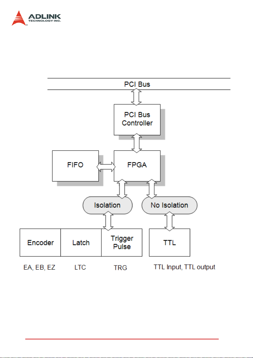
use DLL function library to build up the application. The block diagram of PCI-8124-C is as follows.
Figure 1-1: PCI-8124-C Block Diagram
2Introduction
Page 13

1.1 Features
PCI Rev 2.2, 32-bit/33Mhz Compliment
Support both PCI-X (3.3V) and PCI (5V) slots
Support 4-bit board ID for multiple boards in one system
4 differential quardrature encoder counter input channels
Each encoder counter input pair supports 1/2/4x A/B phase, dual
pulse (CW/CCW) and signed pulse (OUT/DIR) modes
Internal digital filter
4 trigger output channels via both open collector and TTL pins
Trigger pulse width is software programmable from 0.1µs to
3.2765ms
Each trigger output channel is selected from all comparators, man-
ual trigger commands, EZ signal and timers by demands
4 trigger counters that can observe the accuracy of the trigger out-
put pulse quantity
4 comparators for comparing encoder counter and FIFO data
10 comparators for comparing encoder counter and linear data
Each encoder counter source is selected from encoder input pins
or timers
Comparator data is updated by next FIFO data or linear data when
encoder counter is compared and trigger is outputted
14 comparators can select one of 4 trigger output channels individ-
ually
4 channel TTL output pins for general purpose output or trigger
output
4 channel TTL input pins for general purpose or timer start signal
4 channel high speed latch input pins for counters
EZ and Latch input pins can be used for general purpose input
Latch input logic is selectab l e by risi ng or falling edge
Encoder counter clear via EZ input pin as zero operation
Programmable interrupt sources from linear data finished, trig-
gered, FIFO empty/full/low, latched, TTL input on.
Switch setting for trigger output default level while power on
Trigger output pin logic programmable
Provide DLL and driver to support Windows 2K/XP/Vista
Introduction 3
Page 14

1.2 Specifications
Main Chip
Chip Vendor: ACTEL
Model No: A3P1000
Power usage: 3.3V and 1.5V
Reference clock: 40Mhz
Encoder Counters:
Number of channels: 4
Type of wiring: dual differential pairs or single-ended pair
Input Isolated photo coupler: PS9115
Isolated Voltage: 2500 Vrms
Maximum input frequency: 20 MHz (under 4xAB mode)
Supported modes: AB phase x1/2/4, CW/CCW, OUT/DIR
Data length: 32-bit
Digital filter: Yes
Zero Operation: EZ input
Counter Comparators:
Number of comparators: 14
Data length: 32-bit
Trigger pulse width: 0.1µs to 3.2765ms programmable
Internal Timers:
Number of timers: 4
Timer base: 400ns
Resolution: 14-bit
Synchronous start signal: TTL input or register setting
Synchronous stop signal: register setting
4Introduction
Page 15

Trigger Output:
Number of channels: 4
Maximum output frequency: 5Mhz
Output types: Open collector or TTL
Open collector Isolated photo-coupler: PS9115
Open collector Isolated: 2500 Vrms
Continuous triggering method: Timer, FIFO or Linear func-
tion data reloading
Interrupt: Yes, when triggered
Trigger counter: Yes
Comparator FIFO:
Number of FIFO: 4
FIFO depth: 1023x32bits
Interrupt type: Empty/full/low (1/4,1/2,3/4)
Auto reload: Yes, auto reload n ext FIFO data to comparator
when compared
Comparator Linear Function
Number of Linear Functions: 10
Start Address length: 32-bits
Repeat times length: 32-bit
Interval length: 13-bit
Direction length: 1-bit
Interrupt: Yes, when repeat times count to 0
Auto reload: Yes, auto reload next linear data to comparator
when compared
Latch Input
Number of Latch Input pins: 4
Input isolated photo-coupler: PS9115
Isolated Voltage: 2500 Vrms
Band width: 10Mhz
Interrupt: Yes, when latched
Introduction 5
Page 16

TTL Input
Number of input pins: 4
Photo-coupler Isolated: No
TTL input mode: General purpose or timer synchronous
start signal
TTL output
Number of output pins: 4
Photo-coupler Isolated: No
TTL output mode: General purpose output or trigger output
General Specifications
Connectors: 50-pin SCSI-type connector
Operating Temperature: 0C - 70C
Storage Temperature: -20C - 80C
Humidity: 5 - 85%, non-condensing
Power Consumption
Slot power supply (input): +5V DC 5%, 450mA(max)
Slot power supply (input): +12V DC 5%, 100mA(max)
Isolation power is from PCI bus (+12V to isolated +5V DC)
PCB Dimension: 151mm(L) X 107mm(W)
6Introduction
Page 17

1.3 Supported Software
1.3.1 Programming Library
ADLINK provides Windows WDM driver and DLL function library
for the PCI-8124-C. These function libra ries are shipped with the
board. It supports for Windows 2000/XP/Vista.
Introduction 7
Page 18

8Introduction
Page 19

2 Installation
This chapter describes how to inst all the PCI-8124-C. Please follow these steps below:
Check what you have (Section 2.1)
Check the PCB (Section 2.2)
Install the hardware (Section 2.3)
Install the software driver (Section 2.4)
Understanding the I/O signal connections (Chapter 3) and
their operation (Chapter 4)
2.1 Package Contents
Except this User’s Guide, the package also inc ludes the following
items:
PCI-8124-C: 4 channel encoder compare tr igger board
ADLINK All-in-one Compact Disc
If any of these items are missing or damaged, contact the dealer
from whom you purchased the product. Save the shipping materials and carton to ship or store the product in the future.
Installation 9
Page 20
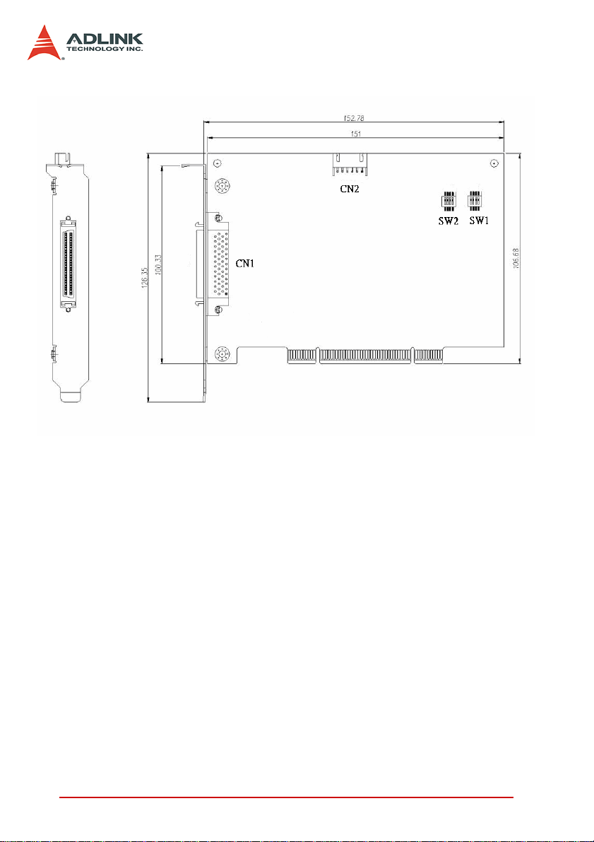
2.2 PCI-8124-C Outline Drawing
Figure 2-1: PCI-8124-C PCB Layout
CN1: SCSI 50 pins Connector
CN2: TTL output
SW1: Board ID switch (ID: 0 to 15)
SW2: Default Trigger Level
10 Installation
Page 21

2.3 PCI-8124-C Hardware Installation
2.3.1 Hardware Configuration
The PCI-8124-C is fully Plug and Play compliant. Hence memory
allocation (I/O port locations) and IRQ channel of the PCI card are
assigned by the system BIOS. The address assignment is done
on a board-by-board basis for all PCI cards in the system.
2.3.2 PCI Slot Selection
Your computer system may have both PCI and ISA slots. Do not
force the PCI card into a PC/A T slot. The PCI-8124 -C can be used
in any PCI slot. It also supports dual voltage PCI bus.
2.3.3 Installation Procedures
1. Read through this manual and setup the board index
with SMD switch. The ID range is from 0 to 15.
2. Turn off your computer. Turn off all accessories (printer,
modem, monitor, etc.) connected to computer. Remove
the cover from your computer.
3. Select a 32-bit PCI expansion slot. PCI slots are shorter
than ISA or EISA slots and are usually white or ivory.
4. Before handling the PCI-8124-C, discharge any static
buildup on your body by touching the metal case of the
computer. Hold the edge of the card and do not touch
the components.
5. Position the board into the PCI slot you have selected.
6. Secure the card in place a t the rear pan el of the system
unit using screws removed from the slot.
2.3.4 Troubleshooting:
If your system doesn’t boot or if you experience erratic operation
with your PCI board in place, it’s most likely caused by an interrupt
conflict (possibly an incorrect ISA setup). In general, the solution,
once determined it is not a simple oversight, is to consult the BIOS
documentation that comes with your system.
Installation 11
Page 22

Check the control panel of the Windows system if the card is listed
by the system. If not, check the PCI settings in the BIOS or use
another PCI slot.
2.4 Software Driver Installation
Using the All-In-One CD with PCI-8124-C package and execute
the following steps:
1. Autorun the ADLINK All-In-One CD.
2. Follow the procedures of the installer.
3. After setup installation is completed, restart windows.
12 Installation
Page 23
2.5 CN1 Pin Assignments
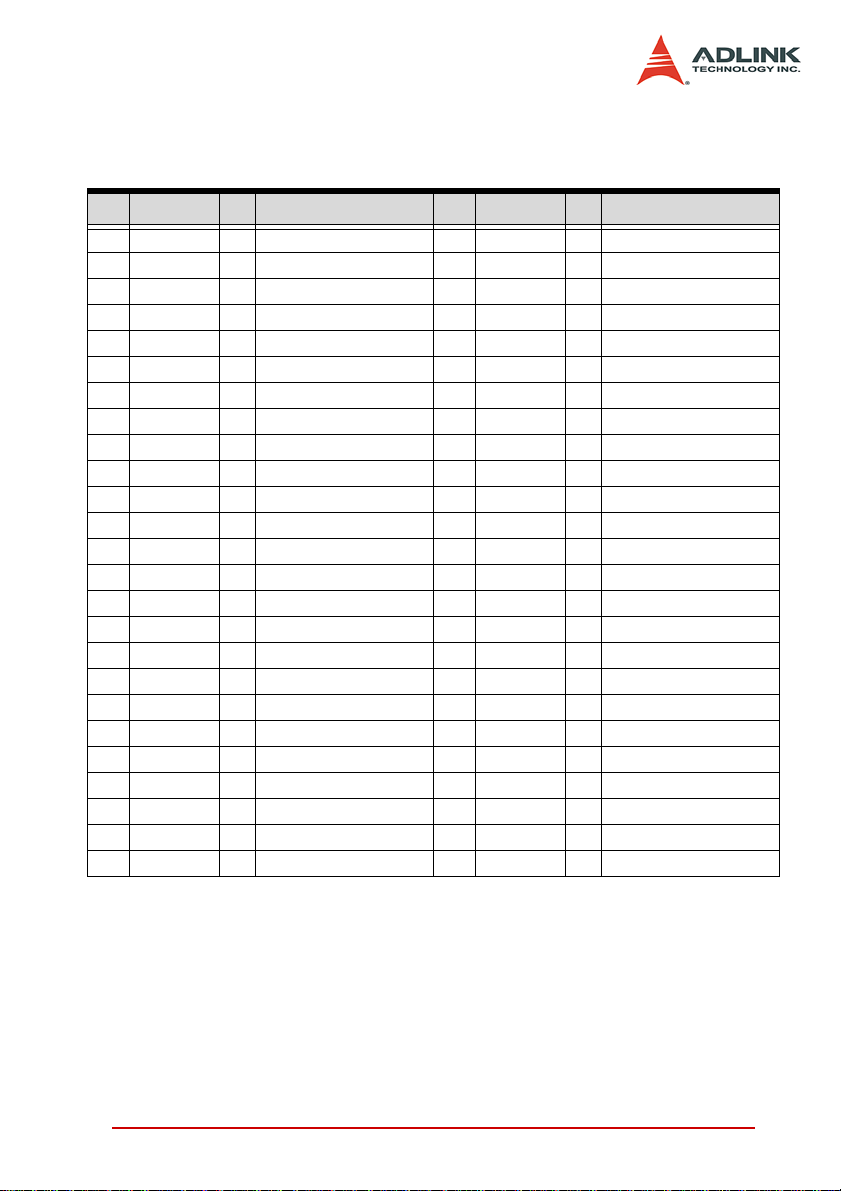
CN1 is the 50-pin SCSI type connector for I/O signals.
No. Name I/O Function No. Name I/O Function
1 INCOM1 - Latch input common 26 INCOM3 - Latch input common
2 LTC1 I Latch input 27 LTC3 I Latch input
3 INCOM2 - Latch input 28 INCOM4 - Latch input common
4 LTC2 I Latch input 29 LTC4 I Latch input
5 EGND - Trigger output common 30 EGND - Latch input common
6 TRG1 O Trigger output 1 31 TRG3 O Trigger output 3
7 EGND - Trigger output common 32 EGND - Trigger output common
8 TRG2 O Trigger output 2 33 TRG4 O Trigger output 4
9 EA1+ I A-phase encoder (+) 34 EA3+ I A-phase encoder (+)
10 EA1- I A-phase encoder (-) 35 EA3- I A-phase encoder (-)
11 EB1+ I B-phase encoder (+) 36 EB3+ I B-phase encoder (+)
12 EB1- I B-phase encoder (-) 37 EB3- I B-phase encoder (-)
13 EZ1+ I Z-phase encoder (+) 38 EZ3+ I Z-phase encoder (+)
14 EZ1- I Z-phase encoder (-) 39 EZ3- I Z-phase encoder (-)
15 EA2+ I A-phase encoder (+) 40 EA4+ I A-phase encoder (+)
16 EA2- I A-phase encoder (-) 41 EA4- I A-phase encoder (-)
17 EB2+ I B-phase encoder (+) 42 EB4+ I B-phase encoder (+)
18 EB2- I B-phase encoder (-) 43 EB4- I B-phase encoder (-)
19 EZ2+ I Z-phase encoder (+) 44 EZ4+ I Z-phase encoder (+)
20 EZ2- I Z-phase encoder (-) 45 EZ4- I Z-phase encoder (-)
21 TTL-IN1 I TTL input signal 46 TTL-IN3 I TTL input signal
22 TTL-IN2 I TTL input signal 47 TTL-IN4 I TTL input signal
23 TTL-OUT1 O TTL output signal 48 TTL-OUT3 O TTL output signal
24 TTL-OUT2 O TTL output signal 49 TTL-OUT4 O TTL output signal
25 DGND - TTL signal ground 50 DGND - TTL signal ground
Table 2-1: CN1 Pin Assignments
Installation 13
Page 24
2.6 CN2 Pin Assignments: TTL Output
CN2 is a 6-pin header as follows:
No. Name I/O Function
1 +5V - +5V power supply
2 TTL-OUT1 O TTL output signal
3 TTL-OUT2 O TTL output signal
4 TTL-OUT3 O TTL output signal
5 TTL-OUT4 O TTL output signal
6 DGND - TTL signal ground
Table 2-2: CN2 Pin Assignments: TTL Output
Note: +5V and DGND pins are provided by the PCI-Bus. There-
fore, these signals are not isolated.
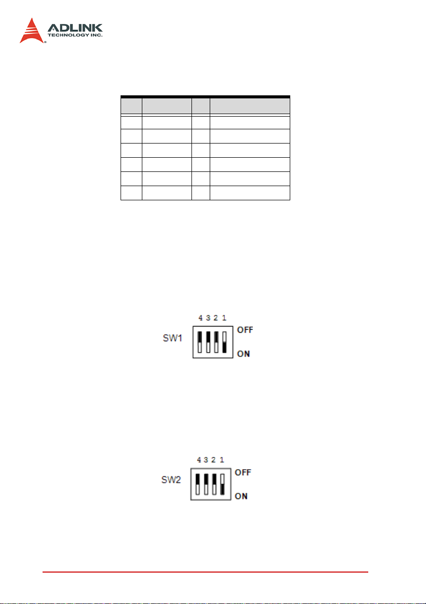
2.7 Board Index Switch Setting
The SW1 switch is used to set board unique index. Its range is
from 0 to 15. For example, the board index is 1 if you switch on pin
1 and switch off pin 2, 3 and 4.
2.8 Default Trigger Level
The SW2 switch is used to set TRG pin’s default level when power
on. Each bit represents one TRG channel. “ON” position means
default level of TRG channel is set to +5V and OFF position
means it is set to 0V. Manufacturing setting is ON.
14 Installation
Page 25

3 Signal Connections
Signal connections of all I/O’s are described in this chapter. Refer
to the contents of this chapter before wiring any cables between
the PCI-8124-C and the end device.
This chapter contains the following sections:
Section 3.1 Connector (CN1) Pin Definition
Section 3.2 Isolated Input Ports (LTC, INCOM)
Section 3.3 Isolated Encoder Differential Input
Section 3.4 Isolated Out pu t Por ts (T RG , EGND)
Section 3.5 TTL Input Ports
Section 3.6 TTL Output Ports
Signal Connections 15
Page 26
3.1 Connector (CN1) Pin Definition
There are 4 Isolated Latch Inputs, 4 A-B-Z Encoder Inputs, 4 TTL
level Inputs, 4 TTL level outputs and 4 Iso lated Outputs on PCI8124-C. The following table shows the pin assignment of CN1.
CN1No. Name I/O Function
1 INCOM1 - Latch input common
2 LTC1 I Latch input
3 INCOM2 - Latch input
4 LTC2 I Latch input
5 EGND - Trigger output reference
6 TRG1 O Trigger output
7 OUTCOM2 - Trigger output reference
8 TRG2 O Trigger output
9 EA1+ I A-phase encoder (+)
10 EA1- I A-phase encoder (-)
11 EB1+ I B-phase encoder (+)
12 EB1- I B-phase encoder (-)
13 EZ1+ I Z-phase encoder (+)
14 EZ1- I Z-phase encoder (-)
15 EA2+ I A-phase encoder (+)
16 EA2- I A-phase encoder (-)
17 EB2+ I B-phase encoder (+)
18 EB2- I B-phase encoder (-)
19 EZ2+ I Z-phase encoder (+)
20 EZ2- I Z-phase encoder (-)
21 TTL-IN1 I TTL input signal
22 TTL-IN2 I TTL input signal
23 TTL-OUT1 O TTL output signal
24 TTL-OUT2 O TTL output signal
25 DGND - TTL signal ground
26 INCOM3 - Latch input common
27 LTC3 I Latch input
28 INCOM4 - Latch input common
16 Signal Connections
Page 27
CN1No. Name I/O Function
29 LTC4 I Latch input
30 EGND - Latch input reference
31 TRG3 O Trigger output
32 EGND - Trigger output reference
33 TRG4 O Trigger output
34 EA3+ I A-phase encoder (+)
35 EA3- I A-phase encoder (-)
36 EB3+ I B-phase encoder (+)
37 EB3- I B-phase encoder (-)
38 EZ3+ I Z-phase encoder (+)
39 EZ3- I Z-phase encoder (-)
40 EA4+ I A-phase encoder (+)
41 EA4- I A-phase encoder (-)
42 EB4+ I B-phase encoder (+)
43 EB4- I B-phase encoder (-)
44 EZ4+ I Z-phase encoder (+)
45 EZ4- I Z-phase encoder (-)
46 TTL-IN3 I TTL input signal
47 TTL-IN4 I TTL input signal
48 TTL-OUT3 O TTL output signal
49 TTL-OUT4 O TTL output signal
50 DGND - TTL signal ground
Signal Connections 17
Page 28
3.2 Isolated Input Ports (LTC, INCOM)
INCOMx
LTCx
Outside PCI-8124 inside PCI-8124
Max 30mA2.2KΩ
7.5mA to 12.5mA
There are 4 pairs of isolated input ports on PCI-8124-C. Each pair
has two terminals. One is INCOMx, and the other is LTCx.
Because the input port of the photo coupler utilized on PCI-8124 -C
is single-directional, LTC signal must be lower than INCOM signal.
When there is a differential voltage between LTCx and corresponding INCOMx, the photo coupler will turn on immediately.
There is an internal resistor in the PCI-8124-C circuit as figure
shows below. So it is not necessary to attach additional resistor
connected outside the PCI-8124-C. The forward current of input
signal is 7.5mA to 12.5mA. The typical forward voltage is 1.65V,
and the maximum forward voltage is 1.9V. So users should calculate the appropriate voltage applied on LTCx and INCOMx.
CN1 Pin No. Name Description
1 INCOM1 In1 Com
3 INCOM2 In2 Com
30 INCOM3 In3 Com
32 INCOM4 In4 Com
2 LTC1 Isolated Latch 1
4 LTC2 Isolated Latch 2
27 LTC3 Isolated Latch 3
29 LTC4 Isolated Latch 4
18 Signal Connections
Page 29
3.3 Isolated Encoder Differential Input
There are 4 pairs of A-B-Z encoder signal inputs on PCI-8124-C.
The pin assignment of these encoder inputs are listed in the following table.
The typical forward voltage of the input diode is 1.65V. And the
forward current of the input diode is 7.5mA to 12.5mA. There is an
internal resistor in the PCI-8124-C circuit as figure shows below.
So if there is no additional resistor connected outside the PCI8124-C, the voltage difference between Encoder+ and Encodershould be lower than 5VDC.
CN1 Pin No. Name Description
9, 15, 34, 40 EAn+ Isolated Encoder A +
10, 16, 35, 41 EAn- Isolated Encoder A 11, 17, 36, 42 EBn+ Isolated Encoder B +
12, 18, 37, 43 EBn- Isolated Encoder B 13, 19, 38, 44 EZn+ Isolated Encoder Z +
14, 20, 39, 45 EZn- Isolated Encoder Z -
Note: n=1, 2, 3, 4
Signal Connections 19
Page 30
3.4 Isolated Output Ports (TRG, EGND)
There are 4 independent isolated output ports on PCI-8124-C.
Because the use of photo coupler PS9115, the output pull high is
not needed. The pin assignment of the isolated output ports on
PCI-8124-C is as follows, and PS9115 output characteristics are
described in the following figure.
CN1 Pin No. Name Description
5 EGND Output reference
7 EGND Output reference
30 EGND Output reference
32 EGMD Output reference
6 TRG1 Trigger 1
8 TRG2 Trigger 2
31 TRG3 Trigger 3
33 TRG4 Trigger 4
20 Signal Connections
Page 31

Outside PCI-8124inside PCI-8124
TRGx
220Ω
Signal Connections 21
Page 32
3.5 TTL Input Ports
There are 4 single ended TTL-level input ports on PCI-8124-C.
The following table shows the pin assignment of these TTL inputs.
CN1 Pin No. Name Description
21 TTL-IN1 TTL Level Input port 1
22 TTL-IN2 TTL Level Input port 2
46 TTL-IN3 TTL Level Input port 3
47 TTL-IN4 TTL Level Input port 4
25, 50 DGND TTL Input reference GND
The maximum input voltage of TTL-level input ports is 4.6VDC. So
user should not apply signals over this limitation.
22 Signal Connections
Page 33

3.6 TTL Output Ports
There are 4 single ended TTL-level output ports on PCI-8124-C.
The following table shows the pin assignment of these TTL outputs.
CN1 Pin No. Name Description
23 TTL-OUT1 TTL Level Output port 1
24 TTL-OUT2 TTL Level Output port 2
48 TTL-OUT3 TTL Level Output port 3
49 TTL-OUT4 TTL Level Output port 4
25, 50 DGND TTL Input reference GND
The maximum output or sink current of each channel is 25mA.
And the maximum output voltage is D5V. User should take care of
these limitations.
Signal Connections 23
Page 34

24 Signal Connections
Page 35

4 Operation Theory
This chapter describes the detail operation of the PCI-8124-C
board. Contents of the following sections are as follows:
Section 4.1: The trigger board overview
Section 4.2: Trigger board operation
Section 4.3: Multiple boards operation
Section 4.4: Interru p t Con tro l
Operation Theory 25
Page 36

4.1 Trigger Board Overview
Timer(4)
Counter(4)
LatchRegister(4)
Comparator(14)
LinearFunction
(10)
FIFO(4)
PWM
&
Mapping
TTLInput(4)
EncoderChannel
(4)
IndexInput(4)
LTCSignals(4)
TRG(4)
TTL(4)
Interrupt
CPU
TriggerCounter
(4)
The input and output relationships are shown as follows:
Inside the PCI-8124-C, all the position comparison and mapping
tasks will be executed within the FPGA. The functional block is as
follows:
The FIFO will automatically load the comparing points into 32-bit
comparator. The comparator will compare the data from counter
26 Operation Theory
Page 37

and FIFO individually. Due to the mapping mechanism, several
combinations are provided for users to continuously send out the
trigger pulse with isolation or non-isolation channels. Latch signal
can let users retain and retrieve the position data at very short
time.
Linear function will automatically load the next comparing points
with a fixed incremental value into 32-bit comparator. Just like
FIFO’s purpose, the new comparing points will be loaded once the
previous comparing point is compared and pulse is triggered.
Operation Theory 27
Page 38

4.1.1 Encoder Channel
The PCI-8124-C has four 32-bit binary up/down counters to keep
the present feedback position from each encoder channel. The
counter counts signal inputs from the EA and EB pin s. The counter
source could be assigned to internal timer.
It accepts 3 types of pulse inputs: (1). Single pulse mode (OUT/
DIR) (2) Dual pulse mode (CW/CCW) (3) 90° phase shifted signals (AB phase mode). 90° phase shifted signals maybe m ultiplied
by a factor of 1, 2 or 4. The 4xAB phase mode is the most commonly used in incremental encoder device. For example, if a
rotary encoder has 2000 pulses per phase (A or B phase), then
the value read from the counter will be 8000 pulses per turn or –
8000 pulses per turn depending on its rotating direction. The three
options will be explained as follows.
Single Pulse Mode (OUT/DIR Mode)
In this mode, EA is dedicated to the count the pulses and EB is to
represent the direction. Simply put, we call it as PULSE/DIR
mode. The DIR signal represents direction as positive (+) or negative (-). User can decide the normal high or normal low for those
two channels according to users’ devices. For example, we set
these two input channel as normal high. The EA can count the
pulse input when the signal level changes from high to low. EB will
see the high level as positive direction unless the level changes to
low level. The waveform is as follows.
28 Operation Theory
Page 39
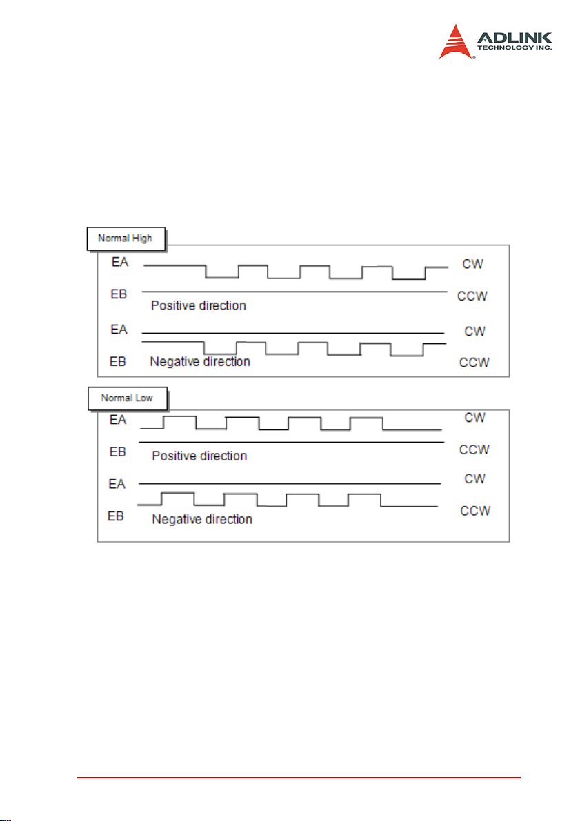
Dual Pulse Mode (CW/CCW Mode)
In this mode, EA is dedicated to count the pulses from external
source and view it as clockwise direction ( CW) . EB is d edica te d t o
count the pulses from external source and view it as counterclockwise direction (CCW). Simply put, EA counts up and EB counts
down. User can decide the normal h igh or normal low for those
two channels according to users’ devices. The following diagr ams
show the normal high and normal low cases individually.
Operation Theory 29
Page 40
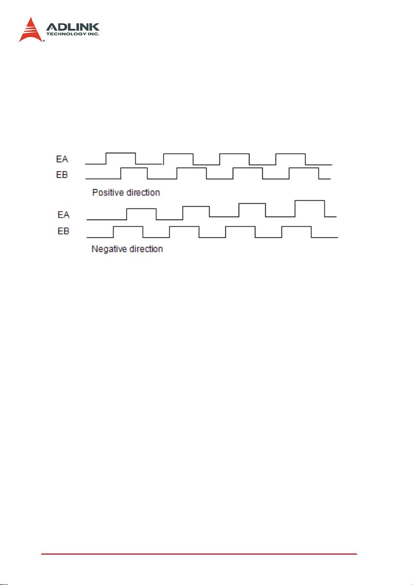
90° phase shifted signals (AB phase Mode)
In this mode, EA signal is a 90° phase leading or lagging to EB
signal. “Lead” or “lag” of phase difference between two signals is
caused by the turning direction of the motor. The up/down counters counts up when the phase of EA signal leads the phase of EB
signal.
The following diagram shows the waveform.
4.1.2 Index Input (EZ)
The index input (EZ) signals of the encoders are used as the
“ZERO” reference. This signal is common on most rotational
motors. EZ can be used to define the absolute position of the
mechanism. The input logic polarity of the EZ signals is programmable with ADLINK library.
With EZ signal, users can realize the homing procedure and clear
the counter as zero.
30 Operation Theory
Page 41
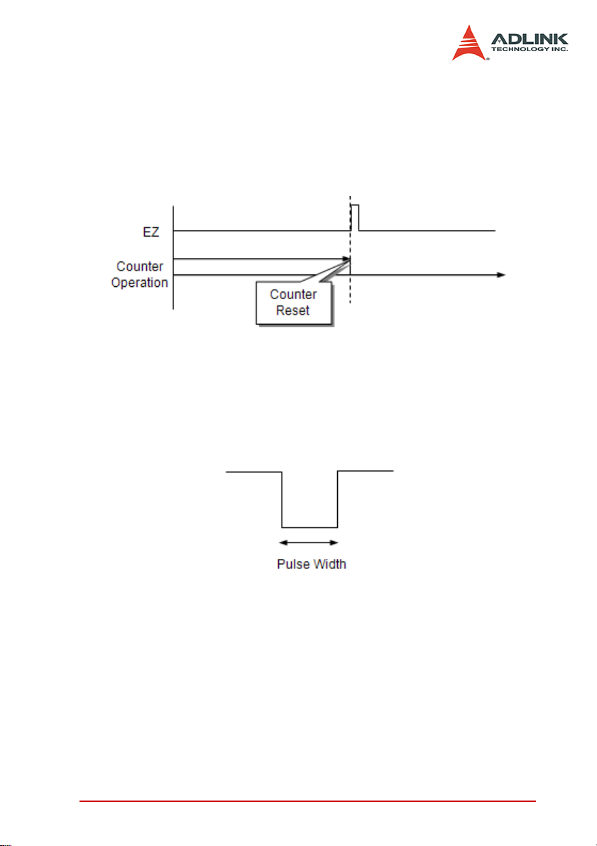
4.1.3 Homing with EZ Signal
The PCI-8124-C can clear the counter value as zero according to
the edge of EZ signal. Homing by edge can let users meet best
homing positioning purpose. Rising or falling edge is supported.
The following diagram shows the case about the homing by rising
edge.
4.1.4 Trigger Pulse Width
For different applications, the trigger pulse width requirement is
different. As for this reason, the trigger pulse width can be adjustable. The available values are from 0.1µs to 3.2765ms. The maximum frequency is up to 5 MHz.
4.1.5 Linear Function
Linear function is used to generate a new comparing position by a
fixed incremental value linear function, Y=Y’+A. Y means a calculated comparing position, the linear data. Y’ means a previous
comparing position. Every time the position is compared, a new
data is calculated by adding ‘A’, the fixed incremental value. This
mechanism makes a the continuous triggering function.
Operation Theory 31
Page 42

4.1.6 FIFO
FIFO is first-in-first-out storage. It is used for storing some preset
position data for comparing. Every time the position is compared,
a new data is retrieve from FIFO into comparator. This mechanism
makes a the continuous triggering function.
4.1.7 PWM & Mapping
PWM is used for adjusting pulse width of trigger. It could also be
switched to a toggle mode. In this mode, the pulse level will
change from low to high or high to low at ever y time when compared.
Mapping means four trigger signals are not one-to-one mapping to
four comparators. For example, Comparator 1 could be linked to
trigger channel 2. Comparator 2 could be linked to trigger channel
1 and 4. Comparator 2 and 4 could be linked to channel 3.
4.1.8 Digital Filter
The digital filter is used to filter noise behind the encoder input circuit. The encoder signals are typically disturbed with environmental noise, and such noise affects the accuracy of the position count
which is generated by calculating the encoder input pulse quantity.
The position counter will increase or decrease because of the
noise blending with the normal encoder signals. In this card, signals over 5 MHz will be filtered which means that the signals are
regarded as noise if its frequency is over 5 MHz. For instance, if
the input signal frequency is 2 M Hz and ac companie d with 8 MH z
noise coupling, after filtered, the 2 MHz will be reserved for the
decoding process.
4.1.9 Trigger Counter
In general, the accuracy of trigger pulse output quantity may be
misjudged because the incorrect image retrieved. During a line
scan process, the frame grabber will trigger the CCD capturing the
line image after receiving the trigger signal from the encoder
board. Therefore, if the encoder does not properly issue a trigger
pulse to frame grabber , then the incorrect imag e may be r etrieved.
However, there are many possibilities will may cause this problem,
32 Operation Theory
Page 43

such as a missing encoder signal, a cable becoming disconnected, abnormal trigger levels, etc. One method to reduce maintenance time is by direct observation of the trigger output pulse
quantity from the embedded trigger counter inside the on-board
FPGA.
Operation Theory 33
Page 44

4.2 Trigger Board Operation
This section describes the operation theory for users to know
more about PCI-8124-C.
4.2.1 Position Comparison
The PCI-8124-C provides position comparison functions for each
channel. Once the counter reache s a pre se t va lu e se t by the user,
the PCI-8124-C will generate the trigger pulse. TRGx pins are for
trigger pulse output channels. Users can also choose TTL Output
pins for this purpose. TRG is an open collector pin.
The comparing method is “equal”. Consequently, when the counter value is exactly equal to the preset value by users, the trigger
pulse will be generated. At the same time, the next comparing
points saved in FIFO or linear function will automatically loaded
into comparator. The following is an exam ple for continuous trig ger
application.
Example: Using the continuous position comparison function.
In this application, the table is controlled by the motion command,
and the CCD Camera is controlled by the position comparison output of the PCI-8124-C. An image of the moving object is easily
obtained.
34 Operation Theory
Page 45

4.2.2 Position Latch
The position latch function is fulfilled by LTC signal. Once the LTC
signal is active, the counter value of its latch channel will be saved
to latched register at the same time. User’s can read the latch register any time.
4.2.3 Linear Function
There are 10 linear functions in PCI-8124-C. Each function is independent. It means that linear function range overlapped is po ssible
when operation. Each linear function has its own comparator and
the comparator could be linked to any one of four counte rs. By this
features, users can produce many kinds of trigger modes. Please
see the following diagram:
Take three linear functions. Set the trigger interval and range as
shown in the diagram. Set these three linear functions to counter3
and also comparator3. Set three linear functions to trigger output
pin TRG1, TRG1, and TRG2 respectively. After these settings,
when the counters start counting from 0 to 10,000, the trigger pins
will output pulses respectively when the compare conditions are
met inside linear function.
Operation Theory 35
Page 46

4.2.4 FIFO Mode
Continuous triggering is fulfilled by linear function and FIFO.
These two modes have their own comparators and can be u sed at
the same time. The FIFO mode is usually used on random comparing data condition. Users can preset these data into FIFO and
perform continuous triggering. Each FIFO has 1023 random comparing data space. If users have more random data than 1023, try
to polling FIFO empty status or wait interrupt event and refill reset
random data.
4.2.5 Timer Function
There are 4 timers on PCI-8124-C. The timer is started by TTL
input and the timer can be set to counters to simulate encoder
inputs. It can also output to trigger pins directly. The timer is
designed by a down-counter. Users must set a counter value into
timer for down counting. Once the timer counter reaches zero, the
timer will output a pulse to trigger pin or increase encoder counter
by 1. The down counting speed is 400ns and the maximum counter value is 14-bit.
36 Operation Theory
Page 47

4.3 Multiple Boards Operation
The maximum installation in one PC system is up to 16 pieces.
This means user can have 64 channels for triggering purpose.
Since the PCI-8124-C is Plug-and-Play compatible, the base
address and IRQ settings for card are automatically assigned by
the BIOS of the system when it is powered on.
When multiple cards are applied to a system, user can select the
unique index number with S1. With this benefit, users can control
each board accordingly without any confusion. For example, if
three PCI-8124-C cards are plugged in to PCI slots, then the corresponding channel number on each card will be:
CH No. CH 1 CH 2 CH 3 CH 4
Card ID
1 0123
2 0123
3 0123
Note: The index number is not accumulated if you have more than
one board in PCI slot.
Operation Theory 37
Page 48

4.4 Interrupt Control
The PCI-8124-C can generate an INT signal to the host PC. Users
have to enable the interrupt service with this function call,
_8124_set_int_factor. On the contrary, the parameter of intFactor
of function is set to 0 to disable the interrupt service.
There are 7 kinds of factors could triggered the PCI-8124-C interrupt. The factors include:
1. PWM:
When PWM received a comparing trigger include manual trig-
ger, it will make an interrupt to host PC.
2. FIFO level:
When the status of FIFO is becoming FIFO level the you set by
the function call “_8124_set_fifo_level”.
3. FIFO empty:
When the FIFO is becoming empty.
4. FIFO full:
When the FIFO is becoming full.
5. LTC:
When the latch counter event is occurred, an interrupt will be
triggered.
6. TTL-IN
When timer is triggered by TTL-IN, an interrupt will be gener-
ated.
7. Linear function
When linear comparing is finish, it will generate an interrupt.
The following table shows the architecture of interrupt factor of
each channel. Notice that the INT factors of last channel (ch 4)
is not the same with the others. It is used to configure the interrupt of linear function.
38 Operation Theory
Page 49

Bit0 1 2 3 4 5 6789
CH
0
1
2
3
4
PWM0 FIFO0 Level FIFO0 Empty FIFO_0 Full LTC0 TTL-IN0 -(*) - - PWM1FIFO1 LevelFIFO1 EmptyFIFO1 FullLTC1TTL-IN1---PWM2FIFO2 LevelFIFO2 EmptyFIFO2 FullLTC2TTL-IN2---PWM3FIFO3 LevelFIFO3 EmptyFIFO3 FullLTC3TTL-IN3----
LIN0 LIN1 LIN2 LIN3 LIN4 LIN5 LIN6 LIN7 LIN8 LIN9
* (-) : reserved bit (set to 0)
Use wait function we provided to wait interrupts under Windows
To detect an interrupt signal from the PCI-8124-C under Windo ws,
we provided an easier way to deal with the interrupt process. The
following steps are described that how you use those interrupt
functions.
Operation Theory 39
Page 50

Steps:
1. Enable the interrupt factors that you want to be wait.
“_8124_get_int_factor”
2. Using wait function to wait the specified interrupt.
“_8124_wait_single_int”
3. In the end of interrupt process, you should disable the
interrupt service.
“_8124_get_int_factor”
Example:
_8124_set_int_factor( CardId, Channel, 0x4); //
FIFO empty
…(FIFO operation)…
// wait FIFO empty interrupt
// FactorBitNum = 2
// 10 seconds time-out
_8124_wait_single_int( CardId, Channel, 2, 10000
);
…
_8124_set_int_factor( CardId, Channel, 0 )//
Disable the interrupt service.
40 Operation Theory
Page 51

5 TriggerMaster Utility
After installing the hardware (Chapters 2 and 3), it is necessary to
correctly configure all cards and double check the system before
running. This chapter gives guidelines for establishing a control system and manually testing the cards to verify correct operation. The TriggerMaster software provides a simple yet powerful
means to setup, configure, test, and debug for trigger system, like
a line scan system that uses 8124-C cards.
Note that TriggerMaster is only available for Windows 2000/XP/
Vista with a screen resolution higher than 1024x768. It cannot be
executed under a DOS environment .
5.1 Running TriggerMaster
After installing the software drivers for the card in Windows 2000/
XP/Vista, the TriggerMaster program can be located at <chosenpath>\PCI-8124-C\TriggerMaster_PCI-8124.exe. To execute the
program, double click on the executable file or use Start -> Program Files -> ADLINK -> PCI-8124-C -> TriggerMaster.
5.2 About TriggerMaster
Before running TriggerMaster please note that TriggerMaster
is a program written in VB.Net 2003, and is available only for
Windows 2000/XP/Vista with a screen resolution higher than
1024x768. It cannot be run under DOS.
TriggerMaster Utility 41
Page 52
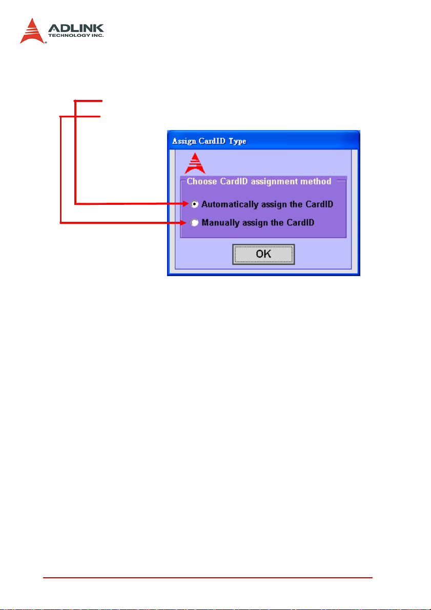
5.3 TriggerMaster Form Introduction
Automatically assign the CardID
Manually assign the CardID
5.3.1 Assign ID Type Dialog
42 TriggerMaster Utility
Page 53

5.3.2 Main Form
3
5
6
2 4
1
1. Card Selected: Choose the card to operate. Note: the
card must be selected first.
2. Show Channel Status:
CNT_# Value: Display the value of encoder counter . The
related function is _8124_get_encoder_value.
Trir_# Times: Display the value of trigger counter. The
related function is _8124_get_pwm_trigger_count.
Next FCMP_# Values: Display the next compared value
in FIFO comparator. The related function is
_8124_get_comparator_data.
FIFO_# Status: Display the status of FIFO comparator.
The related function is _8124_get_fifo_sts.
3. LCMP_Informaton and sketch_of_setting Forms:
Show_LCMP_Information: Display the
Display_Status_LinearCMP form to observe the status
of each linear comparator.
Display sketch_of_setting: Display the sketch_of_setting
form to see the overview of all settings.
4. Tab Switch: Switch the channel and parameter setting
tabs.
7
TriggerMaster Utility 43
Page 54

5. Set Sources:
TRG_# and TTL_# Source: Display the
Set_TRG_&_TTL_Out form to set source, logic and
mode for TRG output and TTL output for TRG_# and
TTL_# output. The related functions ar e
_8124_set_trigger_source,
_8124_set_trgOut_logic, and
_8124_set_ttlOut_source.
PWM_# Source: Display the Choose_PWM_Source
form to set the source for PWM_#. The related function
is _8124_set_pwm_source.
LCMP Source: Display the Set_Linear_Comparator form
to set each linear comparator. The related functions are
_8124_enable_linear_set,
_8124_set_linear_compare, and
_8124_set_linear_source. Note: the setting in this
form is for all channels.
CNT_#: Display the Set_CNT_Source form to set the
source for counter_#. The related function is
_8124_set_counter_source.
Set_Timer_# Interval: Set the interval timer. The unit is
millisecond. The related function is _8124_set_Timer.
6. Set FIFO_# data:
5 Points Test: In this area user can set five data into the
FIFO comparator once to verify the functionality of FIFO
compare. The related function is
_8124_set_fifo_array.
H uge Points Test: In this area user can input a large
number of data into the FIFO comparator. The rela ted
function is _8124_set_fifo_array ().
Note: if FIFO comparator is not selected the source for
the PWM_#, this area is locked.
7. Displays version: Displays the libray, firmware and the
driver version. The related funcion is
_8124_get_version.
44 TriggerMaster Utility
Page 55
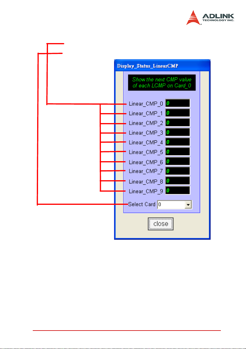
5.3.3 Display _Status_LinearCMP Form
Display the status of linear comparator
Select the card you want to observe
TriggerMaster Utility 45
Page 56

5.3.4 Sketch_of_setting Form
1
This Sketch_of_setting form allows you to conveniently observe
the all settings. When changing any settings, the
Sketch_of_setting form updates immediately.
2 3 4 5
1. Sketch for Card #: Describe which card is showing.
2. TRG and TTL Source: Describe the status of setting of
TRG-OUT and TTL-OUT sources. The light green
means the source is chosen.
3. PWM Source: Describe the status of setting of PWM
source. The light blue means the source is chosen.
Note: the ManTr# is always chosen.
4. LCMP Source: Describe the status of setting of linear
comparator source. The light green means the source is
chosen.
5. CNT Source: Describe the status of setting of counter
source. The light purple means the source is chosen.
46 TriggerMaster Utility
Page 57

5.3.5 Set_TRG_&_TTL_Out Form
In this form, you can set operation logic, operation mode, source,
and En/Disable options for TRG-OUT and TLL-OUT.
1
2
3
1. Set TRG_# source and mode: Set En/Disable and
operation logic for the TRG-OUT. The related function is
_8124_set_trgOut_logic.
2. Select PWM source for TRG_#: Select the PWM
source for TRG-OUT. The related function is
_8124_set_trigger_source.
3. Set TTL_# Mode: Set the TTL-OUT mode to be general
output or be TRG-OUT. The related function is
_8124_set_ttlOut_source.
TriggerMaster Utility 47
Page 58

5.3.6 Choose_PWM_Source Form
In this form, you can choose the source for PWM. Note: the
manual_Trigger is always selected. The related function is
_8124_set_pwm_source.
48 TriggerMaster Utility
Page 59

5.3.7 Set_Linear_Comparator Form
1 2
In this form, you can set the En/Disable, choose source, and set
parameters for each linear comparator.
1. En/Disable: Set En/Disable for each linear comparator.
The related function is _8124_enable_linear_set.
2. Set the source and parameters for linear compara-
tor: Set the source and start point, repeat times and
interval to the linear comparator. The related function is
_8124_set_linear_compare.
TriggerMaster Utility 49
Page 60

5.3.8 Set_CNT_Source Form
In this form, you can set the source for the encoder counter. There
are total eight kinds of input sou rces for encoder coun ter on PCI8124-C. Only one type can be selected at the same time. The
related function is _8124_set_counter_source.
50 TriggerMaster Utility
Page 61

5.3.9 Encoder_# Mode
1
2
3 4 5
6
Enter Set mode and logic tab by clicking the Set mode and logic
tag as show below:
1. Encoder_# Mode: Set the encoding mode for encoder
including OUT/DIR, CW/CCW, 1 xAB phase, 2xAB phase
and 4xAb phase. The related function is
_8124_set_encoder_input_mode.
2. CNT_# Mode: Set the count mode counting up or count-
ing down for counter. The related function is
_8124_set_encoder_up_down_count.
3. EZ_# Clear: En/Disable the EZ clear function. The
related function is _8124_set_ez_clear.
4. Set PWM_#: Set the PWM mode and its width. The
related functions are _8124_set_pwm_mode and
_8124_set_pwm_pulse_width.
5. Set Interrupt Source: Click the Enter button to display
the Set_Interrupt_Source form. In the form, user can set
various interrupts for each channel and linear comparator interrupt for all channels.
6. FIFO_# Low Level: Set the FIFO comparator low level.
The related function is _8124_set_fifo_level.
TriggerMaster Utility 51
Page 62

5.3.10 Set_Interrupt_Source Form
1
2
In this form, you can set the various interrupt events for each
channel and linear comparator interrupt event for all channels.
1. Only for Channel_#: Set the various interrupt events for
channel_#. The related function is
_8124_set_int_factor.
PW M_#: Set the PWM event to the interrupt factor. This
interrupt event occurs when the PWM receives a trigger
single.
FIFO_# Level: Set the FIFO_# level event to the inter-
rupt factor. This interrupt event occurs when the data in
FIFO is less than FIFO level.
52 TriggerMaster Utility
Page 63

FIFO_# Empty: Set the FIFO_# empty event to the inter-
rupt factor. This interrupt event occurs when the FIFO is
empty.
FIFO_# Full: Set the FIFO_# full event to the interrupt
factor. This interrupt event occurs when FIFO is full.
LTC_#: Set the L TC_# event to the interrupt factor. This
interrupt event occurs when specified latch contition
meet.
TTL_IN_#: Set the TTL_IN_# event to the interrupt fac-
tor. Th is interrup t event occurs when T TL_IN_# rece ives
a signal.
2. For all channel: Set the linear comparator event to the
interrupt factor. This interrupt event occurs when the
comparing in linear comparator is finished.
TriggerMaster Utility 53
Page 64
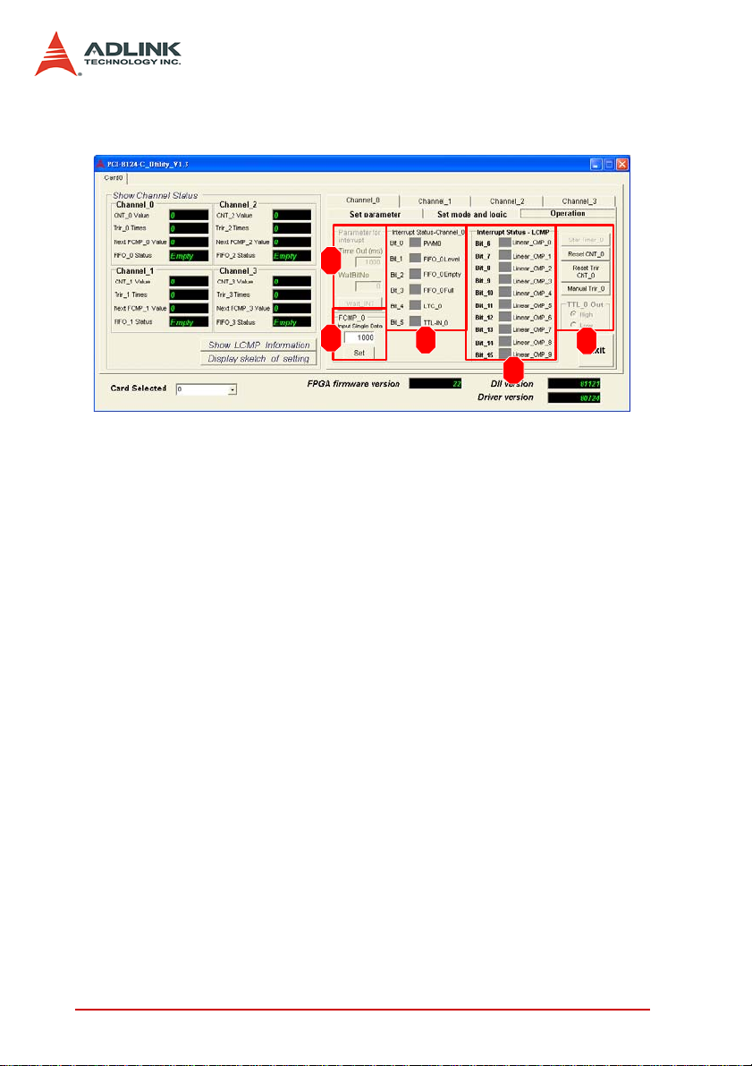
5.3.11 Set_Interrupt_Source form
1
2
4
Enter Operation tab by clicking the Operation tag show as below:
3
51
1. Interrupt parameters:
Time Out (ms): Set the time out for waiting interrupt.
WaitBitNo: Input the bit number which user want to wait
the interrupt.
Wait_INT: Start to wait interrupt. The related function is
_8124_wait_single_int.
2. FCMP_# Input Single Data:
Input single one data into FIFO comparator.
3. Interrupt Status-Channel_#: Show the status of interrupt of each channel; color yellow means waiting, color
green means received interrupt, color green means time
out.
4. Interrupt Status – LCMP: Show the status of interrupt
for linear comparator interrupt; color yellow means waiting, color green means received interrupt, color green
means time out.
54 TriggerMaster Utility
Page 65

5. Buttons:
Start Timer_#: Start the interval timer.
Reset CNT_#: Reset the counter value.
Reset Trir CNT_#: Reset the trigger counter value.
Manual Trir_#: Trigger pulse manually.
TTL_# Out: TTL_out output high or low. If TTL_Out
mode is trg-out, it can’t be operated.
TriggerMaster Utility 55
Page 66

56 TriggerMaster Utility
Page 67

6 Function Library
This chapter describes the supporting software for PCI-8124-C.
User can use these functions to develop programs in C, C++, or
Visual Basic.
6.1 List of Functions
This section details all the functions. The function prototypes an d
common data types are declared in pci_8124.h and type_def.h.
We suggest you use these data types in your application programs. The following table shows the data type names and their
range.
.
Type Name Description Range
U8 8-bit ASCII character 0 to 255
I16 16-bit signed integer -32768 to 32767
U16 16-bit unsigned integer 0 to 65535
I32 32-bit signed long integer -2147483648 to 2147483647
U32 32-bit unsigned long integer 0 to 4294967295
F32 32-bit single-precision floating-point -3.402823E38 to 3.402823E38
F64 64-bit double-precision floating-point
Boolean Boolean logic value TRUE, FALSE
Table 6-1: Data Type Definitions
The functions of the PCI-8124-C’s software drivers use full-names
to represent the functions real meaning. The naming convention
rules are:
In a ‘C’ programming environment:
_{8124}_{action_name (lower case)} e.g. _8124_initial ()
-1.797683134862315E308
to 1.797683134862315E309
In order to recognize the difference between a C library and a VB
library, a capital “B” is placed at he beginning of each function
name e.g. B_8124_initial ().
Function Library 57
Page 68
System: Section 5.2
Function Name Description
_8124_initialSw PCI-8124-C Cards Initialization
_8124_close Release the resources of PCI-8124-C Cards
_8124_get_version Get the hardware and software versions
Encoder & Counter: Section 5.3
Function Name Description
_8124_set_encoder_input_mode Set the pulse input decoded mode
_8124_set_encoder_value Set the encoder’s(counter’s) value
_8124_get_encoder_value Get the encoder’s(counter’s) value
_8124_set_encoder_up_down_count Set count up or count down for counter
_8124_set_ez_clear Configure the EZ clear operation
_8124_set_counter_source Set the source of counter
PWM Configuration: Section 5.4
Function Name Description
_8124_set_pwm_source Set the source of PWM
_8124_set_pwm_mode Set the mode of PWM ( Pulse or Toggle output)
_8124_set_pwm_pulse_width Set the output pulse width
_8124_set_pwm_toggle_dir Set the count direction to toggle the level output
TRG-OUT & TTL-OUT Configuration: Section 5.5
Function Name Description
_8124_set_trigger_source Set the source of TRG-OUT
_8124_set_trgOut_logic Set the logic of TRG-OUT
_8124_set_ttlOut_source Set the source of TTL-OUT
_8124_set_ttlOut Set the TTL-OUT when it is as a digital output
Comparator: Section 5.6
Function Name Description
_8124_set_comparator_data Set the comparing data to the comparator
_8124_get_comparator_data Get current comparing data from the comparator
58 Function Library
Page 69

FIFO Comparing: Section 5.7
Function Name Description
_8124_reset_fifo Reset FIFO data
_8124_get_fifo_sts Get the current FIFO status
_8124_set_fifo_data Set a comparing data to FIFO
_8124_set_fifo_array Set comparing data array to FIFO
_8124_set_fifo_shift Shift the FIFO data to comparator
_8124_set_fifo_level Set the FIFO low level
_8124_get_fifo_level Get the FIFO low level
Linear Comparing: Section 5.8
Function Name Description
_8124_set_linear_compare Set the linear comparing function
_8124_set_linear_source
Set the trigger output sources for linear functions
_8124_enable_linear_set Enable/Disable the linear set
Manual Trigger: Section 5.9
Function Name Description
_8124_manual_trigger Set the trigger output manually
Digital input: Section 5.10
Function Name Description
_8124_get_di_sts Get the digital input signal’s status
Latch: Section 5.11
Function Name Description
_8124_set_latch Configure the latch function
_8124_get_latch_event_sts Get the latch event status
_8124_get_latch_value Get the latched value
Timer: Section 5.12
Function Name Description
_8124_set_Timer Configure the Timer
Function Library 59
Page 70
Function Name Description
_8124_start_timer Start the timer manually
Interrupt Control: Section 5.13
Function Name Description
_8124_set_int_factor Set (Enable) the interrupt factors
_8124_get_int_factor Get the setting of interrupt factors
_8124_wait_single_int Wait the single interrupt event
_8124_reset_int Set the interrupt event to a non-signaled state
Filtering & Monitoring: Section 5.14
Function Name Description
_8124_set_input_filter_enable Enable digital input signal filter
_8124_get_noise_detect Get noise detection status
_8124_get_pwm_trigger_count Get PWM triggered counter
_8124_reset_pwm_trigger_count Reset PWM triggered counter
_8124_get_linear_next_compare Get next linear compare data
_8124_get_linear_remain_trigger_count Get remaining lin ear trigger count
60 Function Library
Page 71

6.2 System & Initialization
@ Name
_8124_initialSw PCI-8124-C Cards Initialization
_8124_close
_8124_get_version Get the hardware and software versions
@ Description
_8124_initialSw:
This function is used to initialize the PCI-8124-C cards in your
system. All PCI-8124-C cards must be initialized by this function before calling other functions. The ID of cards can be
assigned by system automatically or dip switch (SW1) manually.
The source of TRG-OUT and TT L-OUT output signals can be
decided by SW2 or PWM output. See also section 5.5
“_8124_set_trigger_source”.
If DefaultSw = 1, the output signal of TRG-OUT and TTL-OUT
will output as SW2. On the contrary, if DefaultSw = 0, the TRGOUT will output as PWM default setting and TTL-OUT will output D5V ( as a digital output).
Release the resources of PCI-8124-C
Cards
_8124_close:
This function is to close the PCI-8124-C cards an d release its
resources, which must be called at the end of your applications.
_8124_get_version:
Users can get the hardware and software version number by
this function.
Function Library 61
Page 72

@ Syntax
C/C++ (Windows 2000/XP)
I16 _8124_initialSw( I16 *CardIdInBit, I16
ManualId, I16 DefaultSw );
I16 _8124_close();
I16 _8124_get_version(I16 CardId, I32
*Firmware_ver, I32 *Driver_ver, I32
*DLL_ver);
Visual Basic (Windows 2000/XP)
B_8124_initialSw (CardIdInBit As Integer, ByVal
ManualId As Integer, ByVal DefaultSw As
Integer) As Integer
B_8124_close () As Integer
B_8124_get_version (ByVal CardId As Integer,
Firmware_ver As Long, Driver_ver As Long,
DLL_ver As Long) As Integer
@ Arguments
I16 *CardIdInBit: The information of PCI-8124-C cards’ card
ID in bit format.
Ex. CardIdInBit = 0x0009; It means there are two PCI-8124-
C cards in your system
Card_0’s ID = 0, Card_1’s ID = 3
I16 ManualId: Cards’ ID decided by SW1
0: Decided by system,
1:Decided by dip switch(SW1)
I16 DefaultSw: Default output setting.
0: Default output as PWM and Digital out
1: Default output as SW2
I16 CardId: The PCI-8124-C card’s ID number. (0 ~ 15)
I32 *Firmware_ver: The firmware version.
I32 *Driver_ver: The device driver version.
I32 *DLL_ver: The DLL’ version.
62 Function Library
Page 73

6.3 Encoder & Counter
@ Name
_8124_set_encoder_input_mode Set the pulse input decoded mode
_8124_set_encoder_value Set the encoder’s(counte r’s) value
_8124_get_encoder_value Get the encoder’s(counter’s) value
_8124_set_encoder_up_down_count Set count up or count down for counter
_8124_set_ez_clear Configure the EZ clear operation
_8124_set_counter_source Set the source of counter
@ Description
_8124_set_encoder_input_mode:
There are 5 types of pulse input mode(EA/EB) including OUT/
DIR, CW/CCW, 1x , 2x, and 4x AB phase. Choose a correct
encoder input mode before using counter.
_8124_set_encoder_value:
This function is used to set the encoder( counter ) value
directly.
_8124_get_encoder_value:
This function is used to read the current encoder value.
_8124_set_encoder_up_down_count:
This function is used to set the specified encoder to count up or
count down.
_8124_set_ez_clear:
This function is used to enable the function of counter clear by
sensing EZ input signal. If enabled, you should choose falling
edge or rising edge to clear counter. On the contrary, if disabled, the setting of “ClrLogic” will be ignored.
Function Library 63
Page 74

_8124_set_counter_source:
This function is used to set the counter source. The source
could be one of the EA/EB input channels or timers. The
default counter source is EA/EB. About timer, please refer the
section 5.12 Timer.
@ Syntax
C/C++ (Windows 2000/XP)
I16 _8124_set_encoder_input_mode( I16 CardId, I16
Channel, I16 IptMode );
I16 _8124_set_encoder_value( I16 CardId, I16
Channel, I32 EncValue );
I16 _8124_get_encoder_value( I16 CardId, I16
Channel, I32 *EncValue );
I16 _8124_set_encoder_up_down_count(I16 CardId,
I16 Channel, I16 Inverse );
I16 _8124_set_ez_clear( I16 CardId, I16 Channel,
I16 Enable, I16 ClrLogic );
I16 _8124_set_counter_source( I16 CardId, I16
Channel, I16 CtnSrc );
Visual Basic (Windows 2000/XP)
B_8124_set_pls_iptmode (ByVal CardId As Integer,
ByVal Channel As Integer, ByVal IptMode As
Integer) As Integer
B_8124_set_encoder_input_mode (ByVal CardId As
Integer, ByVal Channel As Integer, ByVal
IptMode As Integer) As Integer
B_8124_set_encoder_value (ByVal CardId As
Integer, ByVal Channel As Integer, ByVal
EncValue As Long) As Integer
B_8124_get_encoder_value (ByVal CardId As
Integer, ByVal Channel As Integer, EncValue
As Long) As Integer
B_8124_set_encoder_up_down_count (ByVal CardId As
Integer, ByVal Channel As Integer, ByVal
Inverse As Integer) As Integer
B_8124_set_ez_clear (ByVal CardId As Integer,
ByVal Channel As Integer, ByVal Enable As
Integer, ByVal ClrLogic As Integer) As
Integer
64 Function Library
Page 75

B_8124_set_counter_source (ByVal CardId As
Integer, ByVal Channel As Integer, ByVal
CtnSrc As Integer) As Integer
@ Argument
I16 CardId: The PCI-8124-C card’s ID number.
I16 Channel: The specified channel number. (0 – 3)
I16 IptMode: The pulse input mode.
0: OUT/DIR (default)
1: CW/C CW
2: 1x AB-Phase
3: 2x AB-Phase
4: 4x AB-Phase
I32 EncValue: The encoder (counter) value.
I16 Inverse: Encoder count direction inverse or not
0: Not inverse (default)
1: Inverse
I16 Enable: Enable EZ-clear function
0: Disable (default)
1: Enable
I16 ClrLogic: Clear logic setting
0: Photo couple: OFF ON (Falling edge) clear (default)
1: Photo couple: ON OFF (Rising edge) clear
I16 CtnSrc: The counter’s source (0 – 7)
0 – 3: EA/EB 0 – 3
4 – 7: Timer 0 – 3
Function Library 65
Page 76

6.4 PWM Configuration
@ Name
_8124_set_pwm_source Set the source of PWM
_8124_set_pwm_mode Set the mode of PWM ( Pulse or Toggle output)
_8124_set_pwm_pulse_width Set the output pulse width
_8124_set_pwm_toggle_dir Set the count direction to toggle the level output
@ Description
_8124_set_pwm_source:
This function is used to set the PWM source (trigger source). A
PWM has 3 kinds of source, LIN, CMP and timer respectively.
Those three kind of sources are independently. Users can
enable them at the same time. The default setting is CMP.
_8124_set_pwm_mode:
There are two types of TRG output. One is pulse type output,
the other is level-switch output. Users can select output type by
this function.
_8124_set_pwm_pulse_width:
If you selected the pulse type output as the PWM output. You
can adjust the pulse width by this function.
_8124_set_pwm_toggle_dir:
If you selected the level-switch output as the PWM output, you
can set the toggled condition by this function. There are 3 conditions (count directions) that the level output could be toggled.
@ Syntax
C/C++ (Windows 2000/XP)
I16 _8124_set_pwm_source( I16 CardId, I16
Channel, I16 CmpEn, I16 LinearEn, I16
TimerEn );
66 Function Library
Page 77

I16 _8124_set_pwm_mode( I16 CardId, I16 Channel,
I16 PulseOrToggle );
I16 _8124_set_pwm_pulse_width( I16 CardId, I16
Channel, I16 WidthPara );
I16 _8124_set_pwm_toggle_dir( I16 CardId, I16
Channel, I16 ToggleDir );
Visual Basic (Windows 2000/XP)
B_8124_set_pwm_source (ByVal CardId As Integer,
ByVal Channel As Integer, ByVal CmpEn As
Integer, ByVal LinearEn As Integer, ByVal
TimerEn As Integer) As Integer
B_8124_set_pwm_mode (ByVal CardId As Integer,
ByVal Channel As Integer, ByVal
PulseOrToggle As Integer) As Integer
B_8124_set_pwm_pulse_width (ByVal CardId As
Integer, ByVal Channel As Integer, ByVal
WidthPara As Integer) As Integer
B_8124_set_pwm_toggle_dir (ByVal CardId As
Integer, ByVal Channel As Integer, ByVal
ToggleDir As Integer) As Integer
@ Argument
I16 CardId: The PCI-8124-C card’s ID number.
I16 Channel: The channel’s number of PWM
I16 CmpEn: Enable CMP(FIFO comparing) source (0: Disable, 1:
Enable)
I16 LinearEn: Enable Linear comparing (0: Disable, 1: Enable)
I16 TimerEn: Enable timer source. (0: Disable, 1:Enable)
I16 PulseOrToggle: Select the pulse output or level switch out-
put
0: Puls e ou tp ut
1: Level switch output (toggle output)
I16 WidthPara: The parameter of pulse width. (0 – 8191)
Pulse width(ns) = ( WidthPara × 16 + 4 ) × 25
Function Library 67
Page 78

I16 ToggleDir: Toggled condition select
0: Directionless
1: Count up
2: Count down
68 Function Library
Page 79

6.5 TRG-OUT & TTL-OUT Configuration
@ Name
_8124_set_trigger_source Set the source of TRG-OUT
_8124_set_trgOut_logic Set the logic of TRG-OUT
_8124_set_ttlOut_source Set the source of TTL-OUT
_8124_set_ttlOut Set the TTL-OUT when it is as a digital output
@ Description
_8124_set_trigger_source:
There are two kinds of TGR sources. One is from SW2 setting,
the other is from PWM or DI signals. If you select SW2 setting,
the function will ignore the setting of parameters “PwmInBit”,
“TtlInInBit” and “EzInBit”. On the contrary, If you select PWM/
TTL-IN/EZ as source, you should set the other parameters in
next. They can be “OR” output.
_8124_set_trgOut_logic:
This function is used to set the logic of TRG –OUT output signal.
_8124_set_ttlOut_source:
This function is used to set the source of TTL-OUT output.
There are two sources of TTL-OUT outpu t. One is DO outp ut.
The other is output as the relative channel of TRG-OUT output.
Caution: Because of the logic of TRG-OUT outputs can be
inversed, the logic of TRG-OUT output and TTL-OUT output may opposite.
_8124_set_ttlOut:
When TTL-OUT is set as digital output (DO), you can control it
by this function.
Function Library 69
Page 80

@ Syntax
C/C++ (Windows 2000/XP)
I16 _8124_set_trigger_source( I16 CardId, I16
Channel, I16 GroupSel, I16 PwmInBit, I16
TtlInInBit, I16 EzInBit );
I16 _8124_set_ttlOut_source( I16 CardId, I16
Channel, I16 TtlOutSrc );
I16 _8124_set_ttlOut( I16 CardId, I16 Channel,
I16 TtlOutValue );
Visual Basic (Windows 2000/XP)
B_8124_set_trigger_source (ByVal CardId As
Integer, ByVal Channel As Integer, ByVal
GroupSel As Integer, ByVal PwmInBit As
Integer, ByVal TtlInInBit As Integer, ByVal
EzInBit As Integer) As Integer
B_8124_set_trgOut_logic (ByVal CardId As Integer,
ByVal Channel As Integer, ByVal Logic As
Integer) As Integer
B_8124_set_ttlOut_source (ByVal CardId As
Integer, ByVal Channel As Integer, ByVal
TtlOutSrc As Integer) As Integer
B_8124_set_ttlOut (ByVal CardId As Integer, ByVal
Channel As Integer, ByVal TtlOutValue As
Integer) As Integer
@ Argument
I16 CardId: The PCI-8124-C card’s ID number.
I16 Channel: The channel’s number of TRG-OUT / TTL-OUT.
I16 GroupSel: The TRG-OUT source.
0: Output according to SW2 setting
1: PWM / TTL-IN / EZ signal
I16 PwmInBit: The source of PWM channel in bit format.
Ex: PwmInBit = 0x2, means PWM_1
I16 TtlInInBit: The source of TTL-IN channel in bit format.
Ex: TtlInInBit = 0x6, means TTL-IN1 and TTL-IN_2
70 Function Library
Page 81

I16 EzInBit: The source of EZ channel in bit format.
Ex: EzInBit = 0x1, means EZ_0
I16 TtlOutSrc: The TTL-OUT output source
0: use as Digital output
1: Follow TRG-OUT
I16 TtlOutValue: TTL-OUT output control
0: DGND.
1: D5V.
Function Library 71
Page 82

6.6 Comparator
@ Name
_8124_set_comparator_data Set the comparing data to the comparator
_8124_get_comparator_data Get current comparing data from the comparator
@ Description
_8124_set_comparator_data:
This function is used to override the current comparing data to
the comparator (CMP).
_8124_get_comparator_data:
This function is used to get the current comparing data from
comparator (CMP).
@ Syntax
C/C++ (Windows 2000/XP)
I16 _8124_set_comparator_data( I16 CardId, I16
Channel, I32 CmpData );
I16 _8124_get_comparator_data( I16 CardId, I16
Channel, I32 *CmpData );
Visual Basic (Windows 2000/XP)
B_8124_set_comparator_data (ByVal CardId As
Integer, ByVal Channel As Integer, ByVal
CmpData As Long) As Integer
B_8124_get_comparator_data (ByVal CardId As
Integer, ByVal Channel As Integer, CmpData
As Long) As Integer
@ Argument
I16 CardId: The PCI-8124-C card’s ID number.
I16 Channel: The channel’s number of comparator (CMP).
I32 CmpData: The current comparing data in comparator.
72 Function Library
Page 83

6.7 FIFO Comparing
@ Name
_8124_reset_fifo Reset FIFO data
_8124_get_fifo_sts Get the current FIFO status
_8124_set_fifo_data Set a comparing data to FIFO
_8124_set_fifo_array Set comparing data array to FIFO
_8124_set_fifo_shift Shift the FIFO data to comparator
_8124_set_fifo_level Set the FIFO low level
_8124_get_fifo_level Get the FIFO low level
@ Description
_8124_reset_fifo:
This function is used to reset (clear) the FIFO. The FIFO status
is return “Empty” status, when you issue this function.
_8124_get_fifo_sts:
This function is used to get th e current FIFO sta tus. There are
four status this function would re turn. The value m eaning is as
below figure.
Function Library 73
Page 84

_8124_set_fifo_data:
This function is used to set the specified comparing data to the
FIFO. The capacity of FIFO is 1023. When the status o f FIFO is
full, the data cannot be set into FIFO. This function won’t check
the FIFO status.
_8124_set_fifo_array:
This function is used to set comparing data ar ra y to th e FI F O.
_8124_set_fifo_shift:
This function is used to shift the FIFO data to comparator
(CMP) manually. Generally, when using the FIFO comparing,
the first compared data must shift to the CMP manually via this
function.
_8124_set_fifo_level:
This function is used to set the FIFO low level. There are four
conditions in FIFO low level selection. The default setting is
512 elements remaining in FIFO.
_8124_get_fifo_level:
This function is used to get the setting of FIFO low level.
@ Syntax
C/C++ (Windows 2000/XP)
I16 _8124_reset_fifo( I16 CardId, I16 Channel );
I16 _8124_get_fifo_sts( I16 CardId, I16 Channel,
I16 *FifoSts );
I16 _8124_set_fifo_data( I16 CardId, I16 Channel,
I32 FifoData );
I16 _8124_set_fifo_array( I16 CardId, I16
Channel, I32 *DataArr, I16 ArraySize );
I16 _8124_set_fifo_shift( I16 CardId, I16 Channel
);
I16 _8124_set_fifo_level( I16 CardId, I16
Channel, I16 Level );
I16 _8124_get_fifo_level( I16 CardId, I16
Channel, I16 *Level );
74 Function Library
Page 85

Visual Basic (Windows 2000/XP)
B_8124_reset_fifo (ByVal CardId As Integer, ByVal
Channel As Integer) As Integer
B_8124_get_fifo_sts (ByVal CardId As Integer,
ByVal Channel As Integer, FifoSts As
Integer) As Integer
B_8124_set_fifo_data (ByVal CardId As Integer,
ByVal Channel As Integer, ByVal FifoData As
Long) As Integer
B_8124_set_fifo_array (ByVal CardId As Integer,
ByVal Channel As Integer, DataArr As Long,
ByVal ArraySize As Integer) As Integer
B_8124_set_fifo_shift (ByVal CardId As Integer,
ByVal Channel As Integer) As Integer
B_8124_set_fifo_level (ByVal CardId As Integer,
ByVal Channel As Integer, ByVal Level As
Integer) As Integer
B_8124_get_fifo_level (ByVal CardId As Integer,
ByVal Channel As Integer, Level As Integer)
As Integer
@ Argument
I16 CardId: The PCI-8124-C card’s ID number.
I16 Channel: The channel’s number of FIFO ( 0 – 3 )
I16 *FifoSts: The FIFO status.
0: FIFO datas = Empty
1: Low level FIFO data > Empty
2: Full > FIFO data > Low level
3: FIFO = Full
I32 FifoData: The data to FIFO.
I32 *DataArr: The data array to FIFO
I16 ArraySize: The size of data array to FIFO. ( 1 – 1023 )
Function Library 75
Page 86

I16 Level: The FIFO low level setting.(remaining data numbers
in FIFO)
0: Low level = 0 (Empty)
1: Low level = 256 ( 1/4 FIFO size )
2: Low level = 512 ( 1/2 FIFO size ) (Default)
3: Low level = 768 ( 3/4 FIFO size )
76 Function Library
Page 87

6.8 Linear Comparing
@ Name
_8124_set_linear_compare Set the linear comparing function
_8124_set_linear_source
_8124_enable_linear_set Enable/Disable the linear set
@ Description
_8124_set_linear_compare:
This function is used to configure the line ar comparing trigger
function. Before using linear comparing function, you should
enable the source of PWM from linear function by
“_8124_set_pwm_source”. PCI-8124-C has 10 linear sets can
be used for linear and they can be compared with any counter
arbitrarily. Every set has 3 parameters including starting point
(StartPoint), repeat times (RepeatTimes) and trigger interval
(Interval). The total trigger pulse would be (RepeatTimes + 1)
times. For example, if you set the RepeatTimes as 10, the total
output pulse will be 11. The follow formula is show that how do
you calculate the next triggering position.
Set the trigger output sources for linear
functions
N ex t trig gerin g po sit ion = Start Poin t + Inte rv al x N
N: triggered times, ( N RepeatTimes)
The Interval can be set as a negative value. The comparing
direction is depending on the signed of Interval. Moreover, if
RepeatTimes is set to 0, the linear comparing will not stop until
stopping counting or reset the linear function.
_8124_set_linear_source:
There are 10 linear sets in PCI-8124-C. Use this function to
assign which sets will be used in the specified trigger channel.
One trigger channel can have more then one linear set.
Function Library 77
Page 88

_8124_enable_linear_set:
The PCI-8124-C has 10 linear sets. Before using these linear
sets, enable the linear set by this function. When linear sets are
no longer needed, it is recommended that the the linear set be
disabled, or it could be unexpectedly triggered.
@ Syntax
C/C++ (Windows 2000/XP)
I16 _8124_set_linear_compare( I16 CardId, I16
SetNum, I16 Channel, I32 StartPoint, F64
RepeatTimes, I16 Interval );
I16 _8124_set_linear_source( I16 CardId, I16
Channel, I16 SetNumInBit );
I16 _8124_enable_linear_set( I16 CardId, I16
SetNum, I16 Enable );
Visual Basic (Windows 2000/XP)
B_8124_set_linear_compare (ByVal CardId As
Integer, ByVal SetNum As Integer, ByVal
Channel As Integer, ByVal StartPoint As
Long, ByVal RepeatTimes As Double, ByVal
Interval As Integer) As Integer
B_8124_set_linear_source( ByVal CardId As
Integer, ByVal Channel As Integer, ByVal
SetNumInBit As Integer ) As Integer
B_8124_enable_linear_set( ByVal CardId As
Integer, ByVal SetNum As Integer, ByVal
Enable As Integer )As Integer
@ Argument
I16 CardId: The PCI-8124-C card’s ID number.
I16 SetNum: Linear Setting set’s number (0 - 9)
I16 Channel: The channel of linear output (0 - 3)
I16 SetNumInBit: Linear set number in bit format
I32 StartPoint: The first trigger point.
F64 RepeatTimes: The trigger repeat times. (32 bits integer)
I16 Interval: The linear interval (1 to 8191, -1 to -8191)
78 Function Library
Page 89

I16 Enable: Enable/Disable linear set
0: disable, 1: enable
Function Library 79
Page 90

6.9 Manual Trigger
@ Name
_8124_manual_trigger Set the trigger output manually
@ Description
_8124_manual_trigger:
This function is used to generate one pulse manually.
@ Syntax
C/C++ (Windows 2000/XP)
I16 _8124_manual_trigger( I16 CardId, I16 Channel );
Visual Basic (Windows 2000/XP)
B_8124_manual_trigger (ByVal CardId As Integer,
ByVal Channel As Integer) As Integer
@ Argument
I16 CardId: The PCI-8124-C card’s ID number.
I16 Channel: The channel’s number of PWM( 0 – 3 )
80 Function Library
Page 91

6.10 Digital Input
@ Name
_8124_get_di_sts Get the digital input signal’s status
@ Description
_8124_get_di_sts:
This function is used to get the status of digital inputs. The digital inputs include TTL-IN, LTC and EZ. The parameters are
showed as bit format. The former four bits of pa ra meters repr esent 4 channels of each digital input.
@ Syntax
C/C++ (Windows 2000/XP)
I16 _8124_get_di_sts( I16 CardId, I16
*TtlStsInBit, I16 *LtcStsInBit, I16
*EzStsInBit );
Visual Basic (Windows 2000/XP)
B_8124_get_di_sts (ByVal CardId As Integer,
TtlStsInBit As Integer, LtcStsInBit As
Integer, EzStsInBit As Integer) As Integer
@ Argument
I16 CardId: The PCI-8124-C card’s ID number.
I16 *TtlStsInBit: The TTL-IN status in bit format.
I16 *LtcStsInBit: The LTC status in bit format.
I16 *EzStsInBit: The EZ status in bit format.
Function Library 81
Page 92

6.11 Latch
@ Name
_8124_set_latch Configure the latch function
_8124_get_latch_event_sts Get the latch event status
_8124_get_latch_value Get the latched value
@ Description
_8124_set_latch:
This function is used to enable or disable the high-speed position capture (latch) function and set the latch condition. Whenever the users enable it and configure the latch condition
(Rising or falling active) correctly, the current position will be
latched when it receive the latch signal. Users can check the
latch events by polling “_8124_get_latch_event_sts” or by
using the interrupt function. See also section 5.13 Interrupt
function.
_8124_get_latch_event_sts:
This function is used to check the latch event status. If the latch
function is enabled and the latch condition is met, the status
will become 1 from 0. The event status is read-clear.
_8124_get_latch_value:
When the latch event occurred, you can use this function get
the latched counter value.
@ Syntax
C/C++ (Windows 2000/XP)
I16 _8124_set_latch( I16 CardId, I16 Channel, I16
Enable, I16 EdgeSel );
I16 _8124_get_latch_event_sts( I16 CardId, I16
*LatchEventInBit );
I16 _8124_get_latch_value(I16 CardId, I16
Channel, I32 *LatchValue );
82 Function Library
Page 93

Visual Basic (Windows 2000/XP)
B_8124_set_latch (ByVal CardId As Integer, ByVal
Channel As Integer, ByVal Enable As Integer,
ByVal EdgeSel As Integer) As Integer
B_8124_get_latch_event_sts (ByVal CardId As
Integer, LatchEventInBit As Integer) As
Integer
B_8124_get_latch_value (ByVal CardId As Integer,
ByVal Channel As Integer, LatchValue As
Long) As Integer
@ Argument
I16 CardId: The PCI-8124-C card’s ID number.
I16 Channel: The channel’s number of Latch ( 0 – 3 )
I16 Enable: Enable the Latch function (0: Disable, 1: Enable)
I16 EdgeSel: Latching condition
0: Photo couple: OFF ON (Falling edge) clear
(default)
1: Photo couple: ON OFF (Rising edge) clear
I16 *LatchEventInBit: Latch event status in bit format (Read
clear)
Bit0: Latch0 event status ( 1: Latched occurred , 0: No
Latched )
Bit1: Latch1 event status ( 1: Latched occurred , 0: No
Latched )
Bit2: Latch2 event status ( 1: Latched occurred , 0: No
Latched )
Bit3: Latch3 event status ( 1: Latched occurred , 0: No
Latched )
I32 *LatchValue: The Latched counter value.
Function Library 83
Page 94

6.12 Timer
@ Name
_8124_set_Timer Configure the Timer
_8124_start_timer Start the timer manually
@ Description
_8124_set_Timer:
This function is used to configure the timer. The timer can be
start by external signal (TTL-IN signal) or by software function.
If the timer was triggered, users can stop the timer by issue the
function ”_8124_start_timer”.
_8124_start_timer:
This function is used to start/stop timer manually.
@ Syntax
C/C++ (Windows 2000/XP)
I16 _8124_set_Timer( I16 CardId, I16 Channel, I16
WaitTtlIn , I16 TtlTrigLogic, I16 Interval );
I16 _8124_start_timer( I16 CardId, I16 Channel,
I16 Start );
Visual Basic (Windows 2000/XP)
B_8124_set_Timer (ByVal CardId As Integer, ByVal
Channel As Integer, ByVal WaitTtlIn As
Integer, ByVal TtlTrigLogic As Integer,
ByVal Interval As Integer) As Integer
B_8124_start_timer (ByVal CardId As Integer,
ByVal Channel As Integer, ByVal Start As
Integer) As Integer
@ Argument
I16 CardId: The PCI-8124-C card’s ID number.
I16 Channel: The channel’s number of timer.
84 Function Library
Page 95

I16 WaitTtlIn: Enable TTL-IN start timer (0: Disable, 1:
Enable)
I16 TtlTrigLogic: TTL-IN start timer condition
0: Falling edge of TTL-IN signal
1: Rising edge of TTL-IN signal
I16 Interval: Timer interval ( 0 – 16383)
Timer tick interval = (Interval x 16 + 4) x 25 (ns)
I16 Start: Start timer
0: Stop timer
1: Start timer
Function Library 85
Page 96

6.13 Interrupt
@ Name
_8124_set_int_factor Set (Enable) the interrupt factors
_8124_get_int_factor Get the setting of interrupt factors
_8124_wait_single_int Wait the single in terrupt event
_8124_reset_int
@ Description
_8124_set_int_factor:
This function is used to enable/disable the interrupt source.
Users can use the function, “_8124_wait_single_int” to wait the
specified interrupt. The following table show s the architecture
of interrupt factor of each channel.
Bit0 1 2 3 4 5 6789
CH
0
1
2
3
4
PWM0 FIFO0 Level FIFO0 Empty FIFO_0 Full LTC0 TTL-IN0 -(*) - - PWM1FIFO1 LevelFIFO1 EmptyFIFO1 FullLTC1TTL-IN1---PWM2FIFO2 LevelFIFO2 EmptyFIFO2 FullLTC2TTL-IN2---PWM3FIFO3 LevelFIFO3 EmptyFIFO3 FullLTC3TTL-IN3----
LIN0 LIN1 LIN2 LIN3 LIN4 LIN5 LIN6 LIN7 LIN8 LIN9
Set the interrupt event to a non-signaled
state
(*): reserved bit (set to 0)
_8124_get_int_factor:
This function is used to get current configuration of interrupt
factors in your card.
_8124_wait_single_int:
When the user enabled the interrupt function for specified factors by “_8124_set_int_factor”, it could use this function to wait
a specific interrupt. When this function was running, the process would never stop until the event was be triggered or the
86 Function Library
Page 97

function was time out. This function returns when one of the following occurs:
1. The specified interrupt factor is in the signaled state.
2. The time-out interval elapses.
This function checks the current state of the specified interrupt
factor. If the state is non-signaled, the calling thread enters the
wait state. It uses no processor time while waiting for the INT
state to become signaled or the time-out interval to elapse.
8124_reset_int:
This function sets the specified interrupt event to a non-signaled state. This function is usually put into program before the
"_8124_wait_single_int" function.
@ Syntax
C/C++ (Windows 2000/XP)
I16 _8124_set_int_factor( I16 CardId, I16
Channel, I16 IntFactorsInBit );
I16 _8124_get_int_factor( I16 CardId, I16
Channel, I16 *IntFactorsInBit );
I16 _8124_wait_single_int( I16 CardId, I16
Channel, I16 FactorBitNum, I32 TimeOutMs );
I16 _8124_reset_int( I16 CardId, I16 Channel, I16
FactorBitNum );
Visual Basic (Windows 2000/XP)
B_8124_set_int_factor (ByVal CardId As Integer,
ByVal Channel As Integer, ByVal
IntFactorsInBit As Integer) As Integer
B_8124_get_int_factor (ByVal CardId As Integer,
ByVal Channel As Integer, IntFactorsInBit As
Integer) As Integer
B_8124_wait_single_int (ByVal CardId As Integer,
ByVal Channel As Integer, ByVal FactorBitNum
As Integer, ByVal TimeOutMs As Long) As
Integer
B_8124_reset_int( ByVal CardId As Integer, ByVal
Channel As Integer, ByVal FactorBitNum As
Integer) As Integer
Function Library 87
Page 98

@ Argument
I16 IntFactorsInBit: Interrupt event factor setting in bit format.
I16 FactorBitNum: Specified the bit number of the IntFactorsInBit.
I32 TimeOutMs: Specify the time-out interval, in milliseconds.
If TimeOutMs is zero, the function tests the states of the specified
event and returns immediately. If TimeOutMs is -1, the function’s
time-out interval never elapses (infinite)
88 Function Library
Page 99

6.14 Filtering & Monitoring
@ Name
_8124_set_input_filter_enable Enable digital input signal filter
_8124_get_noise_detect Get noise detection status
_8124_get_pwm_trigger_count Get PWM triggered counter
_8124_reset_pwm_trigger_count Reset PWM triggered counter
_8124_get_linear_next_compare Get next linear co mpare data
_8124_get_linear_remain_trigger_count Get remaining linear trigger count
@ Description
_8124_set_input_filter_enable:
This function is used to enable the digital filter. If the filter is
enabled, pulse width of input signals "EA, EB, EZ and LTC" must
larger than 100 ns or the input signal will be ignore (treat as a
noise).
This function is available after Firmware version: 0x13.
_8124_get_noise_detect:
This function is used to detected whether the signal is a noise or
not. If the width of input signal is less than 100 ns, the status will
be turned ON. The status will be cleared after read.
This function is available after Firmware version: 0x13.
_8124_get_pwm_trigger_count:
This function is used to get PWM trigged counter.
This function is only for debug used. Because It does not have
register latch protection (high word (16-31 bits) latch) of counter
when register read. Therefore, it could be a problem when counter
is count up at mean time you read the counter.
This function is available after Firmware version: 0x13.
_8124_reset_pwm_trigger_count:
This function is used to reset PWM triggered counter.
This function is available after Firmware version: 0x13.
Function Library 89
Page 100

_8124_get_linear_next_compare:
This function is used to get the next linear compare data.
This function is only for debug used. It does not have re gister latch
protection (high word (16-31 bits) latch) of counter when register
read. Therefore, it could be a problem when counter is count up at
mean time you read the counter.
This function is available after Firmware version: 0x13.
_8124_get_linear_remain_trigger_count:
This function is used to get remaining triggered counter.
This counter is a count down counter. You can use this function to
check how many remaining triggered will be output.
This function is available after Firmware version: 0x13.
@ Syntax
C/C++ (Windows 2000/XP)
I16 _8124_set_input_filter_enable( I16 CardId,
I16 Channel, I16 Enable );
I16 _8124_get_noise_detect( I16 CardId, I16
Channel, I16 *DetectStatus );
I16 _8124_get_pwm_trigger_count( I16 CardId, I16
Channel, F64 *PwmCount );
I16 _8124_reset_pwm_trigger_count( I16 CardId,
I16 Channel );
I16 _8124_get_linear_next_compare( I16 CardId,
I16 SetNum, I32 *CmpData );
I16 _8124_get_linear_remain_trigger_count( I16
CardId, I16 SetNum, F64 *Count );
Visual Basic (Windows 2000/XP)
@ Argument
I16 CardId:
I16 Channel: Channel number: 0 ~ 4
90 Function Library
 Loading...