

Page 1

NuDAQ
®
PCI-7442/7443/7444
128-CH/64-CH Isolated Digital I/O Cards
User’s Manual
Manual Rev. 2.50
Revision Date: May 7, 2013
Part No: 50-11218-2010
Advance Technologies; Automate the World.
Page 2

Revision History
Revision Release Date Description of Change(s)
2.01 2007/03/12 Initial Release
2.50 2013/05/07 Updated Package Contents
Copyright 2013 ADLINK TECHNOLOGY INC.
All Rights Reserved.
The information in this document is subject to change without prior
notice in order to improve reliability , design, and function and does
not represent a commitment on the part of the manufacturer.
In no event will the manufacturer be liable for direct, indirect, special, incidental, or consequential damages arising out of the use or
inability to use the product or documentation, even if advised of
the possibility of such damages.
This document contains proprietary information protected by copyright. All rights are reserved. No part of this manual may be reproduced by any mechanical, elec tronic, or other means in a ny form
without prior written permission of the manufacturer.
Trademarks
NuDAQ, NuIPC, DAQBench are registered trademarks of ADLINK
TECHNOLOGY INC.
Product names mentioned herein are used for identification pur-
poses only and may be trademarks and/or registered trademarks
of their respective companies.
Page 3

Getting service
Customer satisfaction is our top priority. Contact us should you
require any service or assistance.
ADLINK TECHNOLOGY INC.
Web Site http://www.adlinktech.com
Sales & Service service@adlinktech.com
Telephone No. +886-2-8226-5877
Fax No. +886-2-8226-5717
Mailing Address 9F No. 166 Jian Yi Road, Chungho City,
ADLINK TECHNOLOGY AMERICA, INC.
Sales & Service info@adlinktech.com
Toll-Free +1-866-4-ADLINK (235465)
Fax No. +1-949-727-2099
Mailing Address 8900 Research Drive, Irvine, CA 92618, USA
ADLINK TECHNOLOGY EUROPEAN SALES OFFICE
Sales & Service emea@adlinktech.com
Toll-Free +49-211-4955552
Fax No. +49-211-4955557
Mailing Address Nord Carree 3, 40477 Düsseldorf, Germany
Taipei Hsien 235, Taiwan, ROC
ADLINK TECHNOLOGY SINGAPORE PTE LTD
Sales & Service singapore@adlinktech.com
Telephone No. +65-6844-2261
Fax No. +65-6844-2263
Mailing Address 84 Genting Lane #07-02A, Cityneon Design
Center, Singapore 349584
ADLINK TECHNOLOGY INDIA LIAISON OFFICE
Sales & Service india@adlinktech.com
Telephone No. +91-80-57605817
Fax No. +91-80-26671806
Mailing Address No. 1357, Ground Floor, "Anupama",
Aurobindo Marg JP Nagar (Ph-1)
Bangalore - 560 078
Page 4

ADLINK TECHNOLOGY BEIJING
Sales & Service market@adlinkchina.com.cn
Telephone No. +82-2-20570565
Fax No. +82-2-20570563
Mailing Address 4F, Kostech Building, 262-2, Yangjae-Dong,
Seocho-Gu, Seoul, 137-130, Korea
ADLINK TECHNOLOGY BEIJING
Sales & Service market@adlinkchina.com.cn
Telephone No. +86-10-5885-8666
Fax No. +86-10-5885-8625
Mailing Address Room 801, Building E, Yingchuangdongli
Plaza, No.1 Shangdidonglu, Haidian District,
Beijing, China
ADLINK TECHNOLOGY SHANGHAI
Sales & Service market@adlinkchina.com.cn
Telephone No. +86-21-6495-5210
Fax No. +86-21-5450-0414
Mailing Address Floor 4, Bldg. 39, Caoheting Science and
Technology Park, No.333 Qinjiang Road,
Shanghai , China
ADLINK TECHNOLOGY SHENZHEN
Sales & Service market@adlinkchina.com.cn
Telephone No. +86-755-2643-4858
Fax No. +86-755-2664-6353
Mailing Address C Block, 2nd Floor, Building A1,
Cyber-tech Zone, Gaoxin Ave. 7.S,
High-tech Industrial Park S., Nanshan District,
Shenzhen, Guangdong Province, China
Page 5

Using this manual
1.1 Audience and scope
This manual guides you when using ADLINK NuDAQ® digital
input/output PCI cards. The card’s hardware and register information are provided for faster application building. This manual is
intended for computer programmers and hardware engineers with
advanced knowledge of data acquisition and high-level programming.
1.2 How this manual is organized
This manual is organized as follows:
Chapter 1 Introduction: This chapter intoduces the NuDAQ
digital input/output PCI cards including the card features, specifications, software support information, and package contents.
Chapter 2 Hardware Information: This chapter presents the
cards’ layout and pin definitions for internal and external connectors.
Chapter 3 Operation Theory: This section illustrates the technology, features, and functions of the cards.
Chapter 4 Register Format: This chapter provides detailed
descriptions of the register formats that are necessary to operate the cards.
War rant y Pol icy : This presents the ADLINK Warranty Policy
terms and coverages.
®
Page 6

1.3 Conventions
Take note of the following conventions used throughout the manual to make sure that you perform certain tasks and instructions
properly.
NOTE Additional information, aids, and tips that help you per-
form particular tasks.
IMPORTANTCritical information and instructions that you MUST perform to
WARNING Information that prevents physical injury, data loss, mod-
complete a task.
ule damage, program corruption etc. when trying to complete a particular task.
Page 7

List of Tables.......................................................................... iii
List of Figures........................................................................ iv
1 Introduction ........................................................................ 1
1.1 Features............................................................................... 2
1.2 Applications ......................................................................... 2
1.3 Specifications....................................................................... 3
1.4 Unpacking Checklist .................. ... ... .... ... ... ... ... .... ... ... ... .... ... 5
1.5 Software Support................................................................. 6
Programming library .................. .... ... ... ........................... 6
DAQ-LVIEW PnP: LabVIEW® Driver .............................6
DAQBenchTM: ActiveX Controls .................................... 7
2 Hardware Information........................................................ 9
2.1 Card Layout........................ .... ... ... ... .... ................................ 9
Bracket Layout ........ ... ... .... ... ... ...................................... 12
2.2 PCI-7442 Pin Assignments................................................ 13
CN2 Connector .............................................................13
CN1 Connector .............................................................15
2.3 PCI-7443 Pin Assignments................................................ 17
CN2 Connector .............................................................17
CN1 Connector .............................................................19
2.4 PCI-7444 Pin Assignments................................................ 21
CN2 Connector .............................................................21
CN1 Connector .............................................................23
2.5 TTL I/O Connector Pin Assignments ................................. 25
JP3 ............................................................................... 25
JP4 ............................................................................... 25
2.6 Board ID (S1)..................................................................... 26
3 Operation theory .............................................................. 27
3.1 Isolated digital input........................................................... 27
3.2 Change of State (COS) interrupt ....................................... 28
Overview ................................. ............................. .........28
COS detection ..............................................................28
COS detection architecture ...........................................29
3.3 Isolated digital output channels ......................................... 30
3.4 Watchdog timer (WDT)...................................................... 31
3.5 Programmable TTL Input/Output....................................... 31
i
Page 8

4 Register Format ................................................................ 33
4.1 PCI-7442 I/O Registers...................................................... 33
Isolated Digital Input Register .......................................33
COS Interrupt Control Registers ............................ ... ... .34
Interrupt Status, COS INT Control Read Back Registers 36
COS Setup/Latch Registers ................... ... ... ... .... ... ... ... .37
TTL IO Setup, Status, DO and DI Registers .................38
Isolated Digital Output and Read Back Registers .........40
Power-up DO Setup/Read Register ..............................42
Watchdog Timer Load, Safety DO Setup/Read Back Regis-
ters .................................. .......... ............ ............. .43
WDT INT Control, Hot-Reset, and Hold Control Register 45
4.2 PCI-7443 I/O Registers...................................................... 47
Isolated Digital Input Registers .....................................47
COS Interrupt Control Registers ............................ ... ... .48
Interrupt Status, COS INT Control Read Back Registers 51
COS Setup/Latch Registers ................... ... ... ... .... ... ... ... .53
TTL IO Setup, Status, DO and DI Register ...................55
4.3 PCI-7444 I/O Registers...................................................... 57
Isolated Digital Output/Read Back Registers ................57
Power-up DO Setup/Read Back Register ................. ... .59
WDT Load Config, Safety DO Setup/Read Back Registers
61
WDT INT Control / Hot-Reset Hold Control Register ....63
TTL IO Setup, Status, DO and DI Registers .................65
4.4 Handling PCI Controller Registers........ .... ...... ... ... .... ... ... ... 67
Warranty Policy ..................................................................... 69
ii
Page 9

List of Tables
Table 2-1: TTL/IO (JP3) Connector Pin Assignments ............. 25
Table 2-2: TTL/IO (JP4) Connector Pin Assignments ............. 25
Table 2-3: Board ID Settings ................................................... 26
List of Tables iii
Page 10

iv List of Tables
Page 11

List of Figures
Figure 2-1: PCI-7442 Layout........................................................ 9
Figure 2-2: PCI-7443 Layout...................................................... 10
Figure 2-3: PCI-7444 Layout...................................................... 11
Figure 2-4: PCI-7440 Series Card Bracket ................................ 12
Figure 2-5: PCI-7440 Series Connector Pin Reference............. 12
Figure 3-1: Photo Coupler.......................................................... 27
Figure 3-2: COS Timing ............................................................. 28
Figure 3-3: COS Detection Architecture..................................... 29
Figure 3-4: Common Ground Connection of
Isolated Digital Output ............................................. 30
iv List of Figures
Page 12

vList of Figures
Page 13

1 Introduction
The ADLINK PCI-7442, PCI-7443, and PCI-7444 cards are highdensity isolated digital I/O cards featuring 128 or 64 channels of
digital input, 128 or 64 channels of digit al output, an d up to 32 TTL
channels for a wide range of PCI bus-based industrial applications.
X PCI-7442: Isolated 64-CH DI and 64-CH DO card
X PCI-7443: Isolated 128-CH DI card
X PCI-7444: Isolated 128-CH DO card
The card series provide a robust 1,250 V
which is suitable for most industrial applications. For PCI chassis
with multiple PCI-7442/7443/7444 installed, the board ID design
feature enables convenient identification of the cards through a
switch jumper, allowing quick troubleshooting and maintenance.
isolation protection
RMS
Introduction 1
Page 14
1.1 Features
Refer to the comparison table belo w for the card series features.
Features PCI-7442 PCI-7443 PCI-7444
32-bit 3.3 V/ 5 V PCI bus, PnP Yes Yes Yes
Isolated digital input channels 64 128 —
Isolated digital output channels 64 — 128
Change-of-state (COS) detection 64 128 —
Channels with 28 V voltage protection 64 128 —
Channels with 250 mA sink current 64 — 128
Channels with digital output status read
back
DO value retained after hot system reset Yes — Yes
Programmable power-up DO status Yes — Yes
Programmable safety DO status
function when WDT interruption occurs
Watchdog timer Yes — Yes
TTL I/O channels 32 32 32
1250 V
Board ID feature Yes Yes Yes
RMS
isolation
64 — 128
Yes—Yes
Yes Yes Yes
1.2 Applications
The PCI-7442/7443/7444 is suitable for these applications:
X Machine automation
X Industrial ON/OFF control
X External relay driving
X Signal switching
X Laboratory automation
2Introduction
Page 15
1.3 Specifications
Optical isolated digital input (PCI-7442/PCI-7443 only)
Input channels 64 (PCI-7442)
128 (PCI-7443)
(Note: Use an efficient cooling system and pay particular
attention to the card and chassis temperature when using
the digital input channels.)
Input voltage High: 5 V – 28 V, non-polarity
Low: 0 V – 1.5 V, non-polarity
Input resistance
Isolated voltage 1250 V
Interrupt source Change of State (COS)
Optical isolated digital output (PCI-7442/PCI-7444 only)
Output channels 64 (PCI-7442)
Output type Open drain power MOSFET driver
Output device TPC8206
Output range 5 V – 40 V
Sink current 250 mA for all channel @ 60°C, 100% duty
Isolation voltage 1250 V
Data transfer Programmed I/O
Isolated +5V power supply (PCI-7442/PCI-7444 only)
Output voltage +5 V
Output current 100 mA maximum at 40°C
Programmable TTL I/O
Number of I/O channels 32
Digital logic level TTL / 3.3 V TTL
Current rating 4 mA (max) per channel
Data transfer Programmed I/O
Watchdog timer (PCI-7442/PCI-7444 only)
Base clock available 10 MHz (fixed)
Counter-width 32-bit
Continued on next page.
4.7 k
Ω
RMS
128 (PCI-7444)
(300 mA max.)
RMS
Introduction 3
Page 16
Safety functions (PCI-7442/PCI-7444 only)
• Programmable power-up DO initial status
• Programmable safety DO status function even during WDT interruption
• Digital output value retention after hot system reset
General specifications
Dimensions 174.7 mm (L) x 106.7 mm (W), standard PCI
Bus 32-bit PCI bus
Operating temperature
Storage temperature
0°C – 60°C
-40°C – 80°C
Humidity 5% to 85% non-condensing
Power
Power consumption PCI-7442: +5 V at 800 mA (typical)
PCI-7443: +5 V at 550 mA (typical)
PCI-7444: +5 V at 800 mA (typical)
Specifications are subject to change without notice.
4Introduction
Page 17
1.4 Unpacking Checklist
Before unpacking, check the shipping carton for any damage. If
the shipping carton and/or contents are damaged, inform your
dealer immediately. Retain the shipping carton and packing materials for inspection. Obtain authorization from your dealer before
returning any product to ADLINK.
Check if the following items are included in the package.
X PCI-7442/PCI-7443/PCI-7444 card
X ADLINK All-in-One CD
X User’s manual
If any of the items is damaged or missing, contact your dealer
immediately.
NOTE The packaging of OEM versions with non-standard con-
figuration, functionality, or package may vary according
to different configuration requests.
CAUTION The boards must be protecte d from static discharg e and
physical shock. Never remove any of the socketed parts
except at a static-free workstation. Use the anti-static bag
shipped with the product to handle the board. Wear a
grounded wrist strap when servicing.
Introduction 5
Page 18

1.5 Software Support
ADLINK provides versatile software drivers and packages to
address different approaches in building a system. Aside fr om programming libraries such as DLLs for many Windows
tems, ADLINK also provides drivers for other software packages
including LabVIEW
®
. All software options may be found in the
ADLINK All-in-One CD.
Programming library
If you are writing you own programs, the following function libraries are available:
DOS Library
For Borland C/C++, and Visual C++, the functions descriptions
are included in this user’s guide.
PCIS-DASK
Included device drivers and DLL for Windows
A DLL is a binary compatible across Windows
XP. That means all applications developed with PCIS-DASK
are compatible across Windows
oping environment can be VB, VC++, Delphi, BC5, or any Win-
®
dows
programming language that allows calls to a DLL. The
user’s guide and function reference manual of PCIS-DASK are
in the CD. Refer to the manual files in the All-in-One CD
(\\Manual_PDF\Software\PCIS-DASK).
These software drivers are shipped with the board. Refer to the
Software Installation Guide for installation procedures.
®
98/NT/2000/XP. The devel-
®
-based sys-
®
98/NT/2000/XP.
®
98/NT/2000/
DAQ-LVIEW PnP: LabVIEW® Driver
DAQ-LVIEW PnP contains VIs that are used to interface with the
LabVIEW
dows
free with the board. You can install and use them without a license.
For more information about DAQ-LVIEW PnP, refer to the user’s
guide in the All-in-One CD.
6Introduction
®
software package. DAQ-LVIEW PnP supports Win-
®
95/98/NT/2000/XP. The LabVIEW® drivers are shipped
Page 19

DAQBenchTM: ActiveX Controls
It is recommended for programmers familiar with ActiveX controls
and VB/VC++ programming to use the DAQBench
trol component library for developing applications. The
DAQBench
For more information about DAQBench
™
is designed under Windows® NT/98 environment.
™
, refer to the user’s guide
™
ActiveX Con-
in the All-in-One CD.
Introduction 7
Page 20

8Introduction
Page 21
2 Hardware Information
This chapter provides information on the PCI-7442/7443/7444
card layout, connectors, and pin assignments.
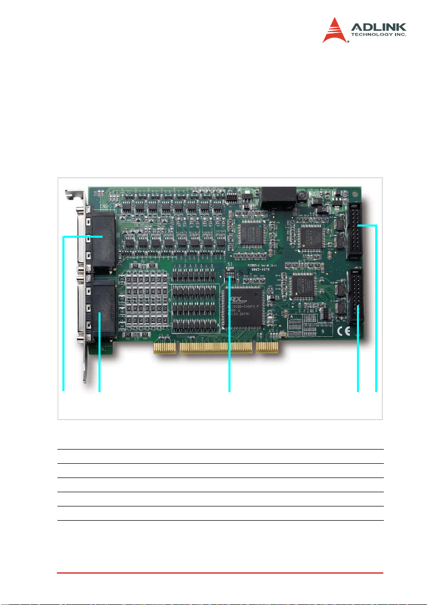
2.1 Card Layout
Figure 2-1 shows the location of the PCI-7442 connectors, switch,
and jumpers.
1
Hardware Information 9
2
Figure 2-1: PCI-7442 Layout
1 CN2 64-CH isolated digital output connector
2 CN1 64-CH isolated digital input connector
3 S1 Board ID DIP switch
4 JP3 16-CH (TTL0~15) TTL I/O connector
5 JP4 16-CH (TTL15~31) TTL I/O connector
3
4
5
Page 22
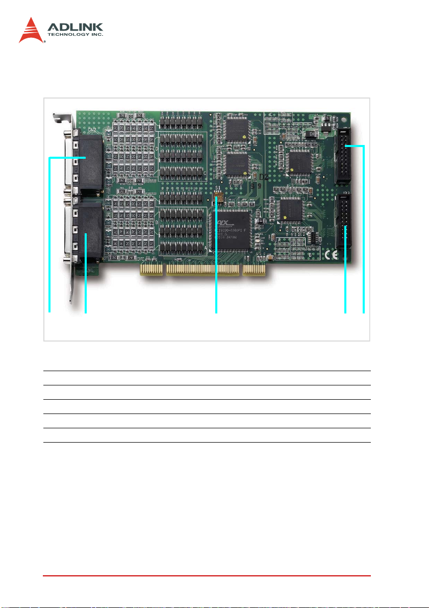
Figure 2-2 shows the location of the PCI-7443 connectors and DIP
switch.
1
10 Hardware Information
2
Figure 2-2: PCI-7443 Layout
1 CN2 64-CH isolated digital input connector (IDI 64~127)
2 CN1 64-CH isolated digital input connector (IDI 0~63)
3 S1 Board ID DIP switch
4 JP3 1 6-CH (TT L0~16) TTL I/O connector
5 JP4 16-CH (TTL16~31) TTL I/O connector
3
4
5
Page 23
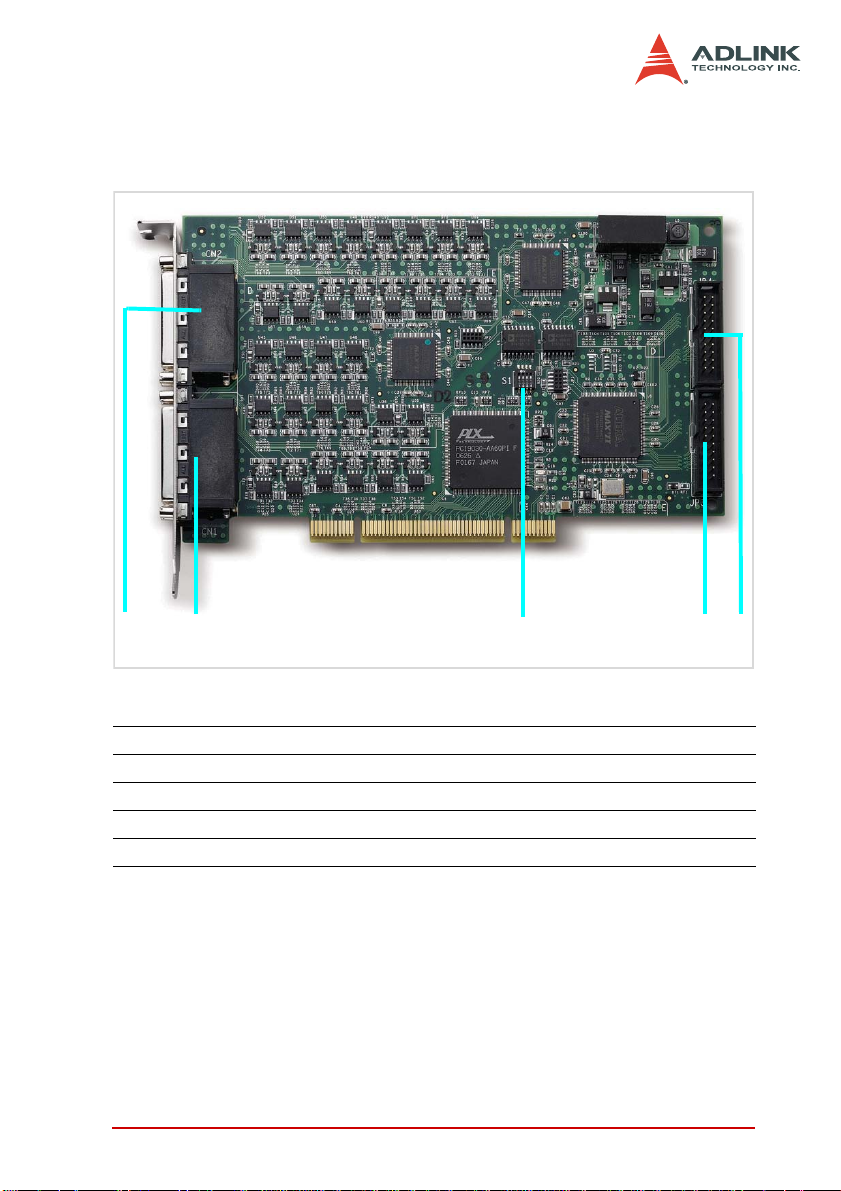
Figure 2-3 shows the location of the PCI-7444 connectors and DIP
switch.
1
Hardware Information 11
2
Figure 2-3: PCI-7444 Layout
1 CN2 64-CH isolated digital output connector (IDO 64~127)
2 CN1 64-CH isolated digital output connector (IDO 0~63)
3 S1 Board ID DIP switch
4 JP3 16-CH (TTL0~15) TTL I/O connector
5 JP4 16-CH (TTL15~31) TTL I/O connector
3
4
5
Page 24
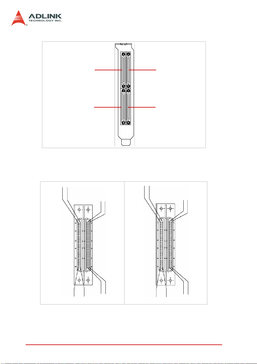
Bracket Layout
CN2B
CN1B
Figure 2-4: PCI-7440 Series Card Bracket
Connector Pin Reference
Terminal B68 Terminal B34
Terminal A1 Terminal A35
CN2B CN2A
CN2A
CN1A
Terminal B68 Terminal B34
Terminal A35 Terminal A1
CN1B CN1A
Terminal B35 Terminal B1
Terminal A68
Terminal A34
Terminal B1 Terminal B35
Terminal A68
Terminal A34
Figure 2-5: PCI-7440 Series Connector Pin Reference
12 Hardware Information
Page 25
2.2 PCI-7442 Pin Assignments
CN2 Connector
CN2B CN2A
V5V B68 B34 V5V IDO_0 A1 A35 IDO_8
IGND
B67 B33 IGND IDO_1 A2 A36 IDO_9
IGND
B66 B32 IGND IDO_2 A3 A37 IDO_10
IGND
B65 B31 IGND IDO_3 A4 A38 IDO_11
IGND
B64 B30 IGND IDO_4 A5 A39 IDO_12
IGND
B63 B29 IGND IDO_5 A6 A40 IDO_13
IGND
B62 B28 IGND IDO_6 A7 A41 IDO_14
IGND
B61 B27 IGND IDO_7 A8 A42 IDO_15
VDD8
B60 B26 VDD7 VDD1 A9 A43 VDD2
IDO_63
IDO_62
IDO_61
IDO_60
IDO_59
IDO_58
IDO_57
IDO_56
IDO_47
IDO_46
IDO_45
IDO_44
IDO_43
IDO_42
IDO_41
IDO_40
B59 B25 IDO_55 IGND A10 A44 IGND
B58 B24 IDO_54 IGND A11 A45 IGND
B57 B23 IDO_53 IGND A12 A46 IGND
B56 B22 IDO_52 IGND A13 A47 IGND
B55 B21 IDO_51 IGND A14 A48 IGND
B54 B20 IDO_50 IGND A15 A49 IGND
B53 B19 IDO_49 IGND A16 A50 IGND
B52 B18 IDO_48 N/C A17 A51 N/C
N/C
B51 B17 N/C IDO_16 A18 A52 IDO_24
IGND
B50 B16 IGND IDO_17 A19 A53 IDO_25
IGND
B49 B15 IGND IDO_18 A20 A54 IDO_26
IGND
B48 B14 IGND IDO_19 A21 A55 IDO_27
IGND
B47 B13 IGND IDO_20 A22 A56 IDO_28
IGND
B46 B12 IGND IDO_21 A23 A57 IDO_29
IGND
B45 B11 IGND IDO_22 A24 A58 IDO_30
IGND
B44 B10 IGND IDO_23 A25 A59 IDO_31
VDD6
B43 B9 VDD5 VDD3 A26 A60 VDD4
B42 B8 IDO_39 IGND A27 A61 IGND
B41 B7 IDO_38 IGND A28 A62 IGND
B40 B6 IDO_37 IGND A29 A63 IGND
B39 B5 IDO_36 IGND A30 A64 IGND
B38 B4 IDO_35 IGND A31 A65 IGND
B37 B3 IDO_34 IGND A32 A66 IGND
B36 B2 IDO_33 IGND A33 A67 IGND
B35 B1 IDO_32 N/C A34 A68 N/C
Hardware Information 13
Page 26

Pin Definition
Pin Definition
IDO_n Isolated digital output channel n
VDD1 common VDD junction for input channel 0-7
VDD2 common VDD junction for input channel 8-15
VDD3 common VDD junction for input channel 16-23
VDD4 common VDD junction for input channel 24-31
VDD5 common VDD junction for input channel 32-39
VDD6 common VDD junction for input channel 40-47
VDD7 common VDD junction for input channel 48-55
VDD8 common VDD junction for input channel 56-63
IGND Ground return path for isolated output channels
V5V Onboard un-regulated 5V power supply output
N/C No Connect
14 Hardware Information
Page 27

CN1 Connector
CN1B CN1A
N/C B68 B34 N/C IDI_0 A1 A35 IDI_8
COM8
COM8
COM8
COM8
COM8
COM8
COM8
COM8
IDI_63
IDI_62
IDI_61
IDI_60
IDI_59
IDI_58
IDI_57
IDI_56
COM6
COM6
COM6
COM6
COM6
COM6
COM6
COM6
IDI_47
IDI_46
IDI_45
IDI_44
IDI_43
IDI_42
IDI_41
IDI_40
B67 B33 COM7 IDI_1 A2 A36 IDI_9
B66 B32 COM7 IDI_2 A3 A37 IDI_10
B65 B31 COM7 IDI_3 A4 A38 IDI_11
B64 B30 COM7 IDI_4 A5 A39 IDI_12
B63 B29 COM7 IDI_5 A6 A40 IDI_13
B62 B28 COM7 IDI_6 A7 A41 IDI_14
B61 B27 COM7 IDI_7 A8 A42 IDI_15
B60 B26 COM7 COM1 A9 A43 COM2
B59 B25 IDI_55 COM1 A10 A44 COM2
B58 B24 IDI_54 COM1 A11 A45 COM2
B57 B23 IDI_53 COM1 A12 A46 COM2
B56 B22 IDI_52 COM1 A13 A47 COM2
B55 B21 IDI_51 COM1 A14 A48 COM2
B54 B20 IDI_50 COM1 A15 A49 COM2
B53 B19 IDI_49 COM1 A16 A50 COM2
B52 B18 IDI_48 N/C A17 A51 N/C
N/C
B51 B17 N/C IDI_16 A18 A52 IDI_24
B50 B16 COM5 IDI_17 A19 A53 IDI_25
B49 B15 COM5 IDI_18 A20 A54 IDI_26
B48 B14 COM5 IDI_19 A21 A55 IDI_27
B47 B13 COM5 IDI_20 A22 A56 IDI_28
B46 B12 COM5 IDI_21 A23 A57 IDI_29
B45 B11 COM5 IDI_22 A24 A58 IDI_30
B44 B10 COM5 IDI_23 A25 A59 IDI_31
B43 B9 COM5 COM3 A26 A60 COM4
B42 B8 IDI_39 COM3 A27 A61 COM4
B41 B7 IDI_38 COM3 A28 A62 COM4
B40 B6 IDI_37 COM3 A29 A63 COM4
B39 B5 IDI_36 COM3 A30 A64 COM4
B38 B4 IDI_35 COM3 A31 A65 COM4
B37 B3 IDI_34 COM3 A32 A66 COM4
B36 B2 IDI_33 COM3 A33 A67 COM4
B35 B1 IDI_32 N/C A34 A68 N/C
Hardware Information 15
Page 28

Pin Definition
Pin Definition
IDI_n Isolated digital input channel n
COM1 common junction for input channel 0-7
COM2 common junction for input channel 8-15
COM3 common junction for input channel 16-23
COM4 common junction for input channel 24-31
COM5 common junction for input channel 32-39
COM6 common junction for input channel 40-47
COM7 common junction for input channel 48-55
COM8 common junction for input channel 56-63
N/C No Connect
16 Hardware Information
Page 29

2.3 PCI-7443 Pin Assignments
CN2 Connector
CN2B CN2A
N/C B68 B34 N/C IDI_64 A1 A35 IDI_72
COM16
COM16
COM16
COM16
COM16
COM16
COM16
COM16
IDI_127
IDI_126
IDI_125
IDI_124
IDI_123
IDI_122
IDI_121
IDI_120
COM14
COM14
COM14
COM14
COM14
COM14
COM14
COM14
IDI_111
IDI_110
IDI_109
IDI_108
IDI_107
IDI_106
IDI_105
IDI_104
B67 B33 COM15 IDI_65 A2 A36 IDI_73
B66 B32 COM15 IDI_66 A3 A37 IDI_74
B65 B31 COM15 IDI_67 A4 A38 IDI_75
B64 B30 COM15 IDI_68 A5 A39 IDI_76
B63 B29 COM15 IDI_69 A6 A40 IDI_77
B62 B28 COM15 IDI_70 A7 A41 IDI_78
B61 B27 COM15 IDI_71 A8 A42 IDI_79
B60 B26 COM15 COM9 A9 A43 COM10
B59 B25 IDI_119 COM9 A10 A44 COM10
B58 B24 IDI_118 COM9 A11 A45 COM10
B57 B23 IDI_117 COM9 A12 A46 COM10
B56 B22 IDI_116 COM9 A13 A47 COM10
B55 B21 IDI_115 COM9 A14 A48 COM10
B54 B20 IDI_114 COM9 A15 A49 COM10
B53 B19 IDI_113 COM9 A16 A50 COM10
B52 B18 IDI_112 N/C A17 A51 N/C
N/C
B51 B17 N/C IDI_80 A18 A52 IDI_88
B50 B16 COM13 IDI_81 A19 A53 IDI_89
B49 B15 COM13 IDI_82 A20 A54 IDI_90
B48 B14 COM13 IDI_83 A21 A55 IDI_91
B47 B13 COM13 IDI_84 A22 A56 IDI_92
B46 B12 COM13 IDI_85 A23 A57 IDI_93
B45 B11 COM13 IDI_86 A24 A58 IDI_94
B44 B10 COM13 IDI_87 A25 A59 IDI_95
B43 B9 COM13 COM11 A26 A60 COM12
B42 B8 IDI_103 COM11 A27 A61 COM12
B41 B7 IDI_102 COM11 A28 A62 COM12
B40 B6 IDI_101 COM11 A29 A63 COM12
B39 B5 IDI_100 COM11 A30 A64 COM12
B38 B4 IDI_99 COM11 A31 A65 COM12
B37 B3 IDI_98 COM11 A32 A66 COM12
B36 B2 IDI_97 COM11 A33 A67 COM12
B35 B1 IDI_96 N/C A34 A68 N/C
Hardware Information 17
Page 30

Pin Definition
Pin Definition
IDI_n Isolated digital input channel n
COM9 common junction for input channel 64-71
COM10 common junction for input channel 72-79
COM11 common junction for input channel 80-87
COM12 common junction for input channel 88-95
COM13 common junction for input channel 96-103
COM14 common junction for input channel 104-111
COM15 common junction for input channel 112-119
COM16 common junction for input channel 120-127
N/C No Connect
18 Hardware Information
Page 31

CN1 Connector
CN1B CN1A
N/C B68 B34 N/C IDI_0 A1 A35 IDI_8
COM8
COM8
COM8
COM8
COM8
COM8
COM8
COM8
IDI_63
IDI_62
IDI_61
IDI_60
IDI_59
IDI_58
IDI_57
IDI_56
COM6
COM6
COM6
COM6
COM6
COM6
COM6
COM6
IDI_47
IDI_46
IDI_45
IDI_44
IDI_43
IDI_42
IDI_41
IDI_40
B67 B33 COM7 IDI_1 A2 A36 IDI_9
B66 B32 COM7 IDI_2 A3 A37 IDI_10
B65 B31 COM7 IDI_3 A4 A38 IDI_11
B64 B30 COM7 IDI_4 A5 A39 IDI_12
B63 B29 COM7 IDI_5 A6 A40 IDI_13
B62 B28 COM7 IDI_6 A7 A41 IDI_14
B61 B27 COM7 IDI_7 A8 A42 IDI_15
B60 B26 COM7 COM1 A9 A43 COM2
B59 B25 IDI_55 COM1 A10 A44 COM2
B58 B24 IDI_54 COM1 A11 A45 COM2
B57 B23 IDI_53 COM1 A12 A46 COM2
B56 B22 IDI_52 COM1 A13 A47 COM2
B55 B21 IDI_51 COM1 A14 A48 COM2
B54 B20 IDI_50 COM1 A15 A49 COM2
B53 B19 IDI_49 COM1 A16 A50 COM2
B52 B18 IDI_48 N/C A17 A51 N/C
N/C
B51 B17 N/C IDI_16 A18 A52 IDI_24
B50 B16 COM5 IDI_17 A19 A53 IDI_25
B49 B15 COM5 IDI_18 A20 A54 IDI_26
B48 B14 COM5 IDI_19 A21 A55 IDI_27
B47 B13 COM5 IDI_20 A22 A56 IDI_28
B46 B12 COM5 IDI_21 A23 A57 IDI_29
B45 B11 COM5 IDI_22 A24 A58 IDI_30
B44 B10 COM5 IDI_23 A25 A59 IDI_31
B43 B9 COM5 COM3 A26 A60 COM4
B42 B8 IDI_39 COM3 A27 A61 COM4
B41 B7 IDI_38 COM3 A28 A62 COM4
B40 B6 IDI_37 COM3 A29 A63 COM4
B39 B5 IDI_36 COM3 A30 A64 COM4
B38 B4 IDI_35 COM3 A31 A65 COM4
B37 B3 IDI_34 COM3 A32 A66 COM4
B36 B2 IDI_33 COM3 A33 A67 COM4
B35 B1 IDI_32 N/C A34 A68 N/C
Hardware Information 19
Page 32

Pin Definition
Pin Definition
IDI_n Isolated digital input channel n
COM1 common junction for input channel 0-7
COM2 common junction for input channel 8-15
COM3 common junction for input channel 16-23
COM4 common junction for input channel 24-31
COM5 common junction for input channel 32-39
COM6 common junction for input channel 40-47
COM7 common junction for input channel 48-55
COM8 common junction for input channel 56-63
N/C No Connect
20 Hardware Information
Page 33

2.4 PCI-7444 Pin Assignments
CN2 Connector
CN2B CN2A
V5V B68 B34 V5V IDO_64 A1 A35 IDO_72
IGND
B67 B33 IGND IDO_65 A2 A36 IDO_73
IGND
B66 B32 IGND IDO_66 A3 A37 IDO_74
IGND
B65 B31 IGND IDO_67 A4 A38 IDO_75
IGND
B64 B30 IGND IDO_68 A5 A39 IDO_76
IGND
B63 B29 IGND IDO_69 A6 A40 IDO_77
IGND
B62 B28 IGND IDO_70 A7 A41 IDO_78
IGND
B61 B27 IGND IDO_71 A8 A42 IDO_79
VDD16
IDO_127
IDO_126
IDO_125
IDO_124
IDO_123
IDO_122
IDO_121
IDO_120
VDD14
IDO_111
IDO_110
IDO_109
IDO_108
IDO_107
IDO_106
IDO_105
IDO_104
B60 B26 VDD15 VDD9 A9 A43 VDD10
B59 B25 IDO_119 IGND A10 A44 IGND
B58 B24 IDO_118 IGND A11 A45 IGND
B57 B23 IDO_117 IGND A12 A46 IGND
B56 B22 IDO_116 IGND A13 A47 IGND
B55 B21 IDO_115 IGND A14 A48 IGND
B54 B20 IDO_114 IGND A15 A49 IGND
B53 B19 IDO_113 IGND A16 A50 IGND
B52 B18 IDO_112 N/C A17 A51 N/C
N/C
B51 B17 N/C IDO_80 A18 A52 IDO_88
IGND
B50 B16 IGND IDO_81 A19 A53 IDO_89
IGND
B49 B15 IGND IDO_82 A20 A54 IDO_90
IGND
B48 B14 IGND IDO_83 A21 A55 IDO_91
IGND
B47 B13 IGND IDO_84 A22 A56 IDO_92
IGND
B46 B12 IGND IDO_85 A23 A57 IDO_93
IGND
B45 B11 IGND IDO_86 A24 A58 IDO_94
IGND
B44 B10 IGND IDO_87 A25 A59 IDO_95
B43 B9 VDD13 VDD11 A26 A60 VDD12
B42 B8 IDO_103 IGND A27 A61 IGND
B41 B7 IDO_102 IGND A28 A62 IGND
B40 B6 IDO_101 IGND A29 A63 IGND
B39 B5 IDO_100 IGND A30 A64 IGND
B38 B4 IDO_99 IGND A31 A65 IGND
B37 B3 IDO_98 IGND A32 A66 IGND
B36 B2 IDO_97 IGND A33 A67 IGND
B35 B1 IDO_96 N/C A34 A68 N/C
Hardware Information 21
Page 34

Pin Definition
Pin Definition
IDO_n Isolated digital output channel n
VDD9 common VDD junction for input channel 64-71
VDD10 common VDD junction for input channel 72-79
VDD11 common VDD junction for input channel 80-87
VDD12 common VDD junction for input channel 88-95
VDD13 common VDD junction for input channel 96-103
VDD14 common VDD junction for input chan nel 104-111
VDD15 common VDD junction for input chan nel 112-119
VDD16 common VDD junction for input chan nel 120-127
IGND Ground return path for isolated output channels
V5V Onboard un-regulated 5V power supply output
N/C No Connect
22 Hardware Information
Page 35

CN1 Connector
CN1B CN1A
N/C B68 B34 N/C IDO_0 A1 A35 IDO_8
IGND
B67 B33 IGND IDO_1 A2 A36 IDO_9
IGND
B66 B32 IGND IDO_2 A3 A37 IDO_10
IGND
B65 B31 IGND IDO_3 A4 A38 IDO_11
IGND
B64 B30 IGND IDO_4 A5 A39 IDO_12
IGND
B63 B29 IGND IDO_5 A6 A40 IDO_13
IGND
B62 B28 IGND IDO_6 A7 A41 IDO_14
IGND
B61 B27 IGND IDO_7 A8 A42 IDO_15
VDD8
B60 B26 VDD7 VDD1 A9 A43 VDD2
IDO_63
IDO_62
IDO_61
IDO_60
IDO_59
IDO_58
IDO_57
IDO_56
IDO_47
IDO_46
IDO_45
IDO_44
IDO_43
IDO_42
IDO_41
IDO_40
B59 B25 IDO_55 IGND A10 A44 IGND
B58 B24 IDO_54 IGND A11 A45 IGND
B57 B23 IDO_53 IGND A12 A46 IGND
B56 B22 IDO_52 IGND A13 A47 IGND
B55 B21 IDO_51 IGND A14 A48 IGND
B54 B20 IDO_50 IGND A15 A49 IGND
B53 B19 IDO_49 IGND A16 A50 IGND
B52 B18 IDO_48 N/C A17 A51 N/C
N/C
B51 B17 N/C IDO_16 A18 A52 IDO_24
IGND
B50 B16 IGND IDO_17 A19 A53 IDO_25
IGND
B49 B15 IGND IDO_18 A20 A54 IDO_26
IGND
B48 B14 IGND IDO_19 A21 A55 IDO_27
IGND
B47 B13 IGND IDO_20 A22 A56 IDO_28
IGND
B46 B12 IGND IDO_21 A23 A57 IDO_29
IGND
B45 B11 IGND IDO_22 A24 A58 IDO_30
IGND
B44 B10 IGND IDO_23 A25 A59 IDO_31
VDD6
B43 B9 VDD5 VDD3 A26 A60 VDD4
B42 B8 IDO_39 IGND A27 A61 IGND
B41 B7 IDO_38 IGND A28 A62 IGND
B40 B6 IDO_37 IGND A29 A63 IGND
B39 B5 IDO_36 IGND A30 A64 IGND
B38 B4 IDO_35 IGND A31 A65 IGND
B37 B3 IDO_34 IGND A32 A66 IGND
B36 B2 IDO_33 IGND A33 A67 IGND
B35 B1 IDO_32 N/C A34 A68 N/C
Hardware Information 23
Page 36

Pin Definition
Pin Definition
IDO_n Isolated digital output channel n
VDD1 common VDD junction for input channel 0-7
VDD2 common VDD junction for input channel 8-15
VDD3 common VDD junction for input channel 16-23
VDD4 common VDD junction for input channel 24-31
VDD5 common VDD junction for input channel 32-39
VDD6 common VDD junction for input channel 40-47
VDD7 common VDD junction for input channel 48-55
VDD8 common VDD junction for input channel 56-63
IGND Ground return path for isolated output channels
N/C No Connect
24 Hardware Information
Page 37

2.5 TTL I/O Connector Pin Assignments
JP3
Pin Function Pin Function
1 TTLIO_0 2 TTLIO_8
3 TTLIO_1 4 TTLIO_9
5 TTLIO_2 6 TTLIO_10
7 TTLIO_3 8 TTLIO_11
9SGND10SGND
11 TTLIO_4 12 TTLIO_12
13 TTLIO_5 14 TTLIO_13
15 TTLIO_6 16 TTLIO_14
17 TTLIO_7 18 TTLIO_15
19 SGND 20 SGND
Table 2-1: TTL/IO (JP3) Connector Pin Assignments
JP4
Pin Function Pin Function
1TTLIO_162TTLIO_24
3TTLIO_174TTLIO_25
5TTLIO_186TTLIO_26
7TTLIO_198TTLIO_27
9SGND10SGND
1 1 TTLIO_20 12 TTLIO_28
13 TTLIO_21 14 TTLIO_29
15 TTLIO_22 16 TTLIO_30
17 TTLIO_23 18 TTLIO_31
19 SGND 20 SGND
Table 2-2: TTL/IO (JP4) Connector Pin Assignments
TTLIO_n TTL I/O channel n
SGND System ground for PCI-7440 card series
Hardware Information 25
Page 38

2.6 Board ID (S1)
The Board ID feature helps you identify the modules when two or
more PCI-7440 Series cards are installed in one system. According to a DIP switch configuration located in the S1, you can assign
a specific board ID to a designated card and access it correctly
through simple software programming.
The table below shows all the switch settings. 1 means DIP is at
ON position; 0 means that the DIP is OFF.
Note: 1 = ON, 0 = OFF
Default setting is 1111 or
Board ID = 0
Table 2-3: Board ID Settings
Board ID
01111
10111
21011
30011
41101
50101
61001
70001
81110
90110
10 1010
11 0010
12 1100
13 0100
14 1000
15 0000
Switch No.
1 2 3 4
26 Hardware Information
Page 39

3 Operation theory
3.1 Isolated digital input
The PCI-7442/7443 card comes with 64/128 opto-isolated digital
input channels. The circuit diagram of the isolated input channel is
shown in Figure 3-1.
Figure 3-1: Photo Coupler
The digital input is routed first through a photo-coupler (PC3H4) so
that the connection are not polarly sensitive whether usi ng positive
or negative voltage. The normal input voltage range for high state
is from 5 V to 28 V.
Operation theory 27
Page 40

3.2 Change of State (COS) interrupt
Overview
The COS (Change of State) means either the input state (logic
level) changes from low to high, or from high to low. The COS
detection circuit will detect the edge of level change. In the PCI7442/7443 card, the COS detection circuit is applied to all the
input channels. When any channel changes its logic level, the
COS detection circuit generates an interrupt request to PCI controller.
COS detection
Figure 3-2 is an example of an 8-CH COS operation. All of the
enabled DI channels’ signal level change will be detected to generate the interrupt request.
While the interrupt request generates, the corresponding DI data
will also be latched into the COS latch register. In our COS architecture, the DI data are sampled by a 33 MHz clock. It means the
pulse width of the digital input have to last longer than 31 ns, or the
COS latch register won’t latch the correct input data. The COS
latch register will be erased after clearing the interrupt request.
Figure 3-2: COS Timing
28 Operation theory
Page 41

COS detection architecture
The COS interrupt system is used in PCI-7442/7443. COS interrupt occurs when the any of enabled DI line sense the status
changes either from HIGH to LOW or from LOW to HIGH. The
COS interrupt system can generate an interrupt request signal and
the software can service this request with ISR. Note that PCI-7442
has two banks (bank 0 from DI0 to DI31 and bank 1 from DI32 to
63) while PCI-7443 has four banks (bank 0 from DI0 to DI31 and
bank 1 from DI32 to 63; bank 2 from DI64 to DI95 and bank 3 from
DI96 to 127). These banks are cascaded together toward the
same IRQ line via CPLD. You can use commands to know which
bank or which DI line has COS when it happens. Also, you can
use commands to disable or enable the COS function of cert ain DI
lines. The COS function for each is disabled by default. Refer to
Figure 3-3 for the COS detection architecture.
CN1
CN2
Figure 3-3: COS Detection Architec t ur e
Operation theory 29
Page 42

3.3 Isolated digital output channels
The common ground connection of isolated digital output is shown
in the figure below. When the isolated digital output goes ON, the
sink current will be conducted through the power MOSFETs. When
the isolated digital output goes OFF, no current is conducted to
flow through the power MOSFETS. Take note that when the load
is of an inductance nature such as a re lay, coil or motor, the VDD
pin must be connected to an external power source. The extra
connection is utilized for the fly-wheel diode to form a currentrelease closed loop, so that the MOSFETs are protected from any
high reverse voltage which can be generated by the inductance
load when the output is switched from ON to OFF. In addition, you
can read back the 64-/128-CH IDO statuses to che ck if the statuses meet your purpose.
x: 0~63
x: 0~127
Figure 3-4: Common Ground Connection of Isolated Digital Output
The PCI-7442/PCI-7444 provides three special fun ctions for safe ty
measures. First, the PCI-7442/PCI-7444 could automatically configure the 64-/128-CH DO initial statuses when powering up. Second, you can direct the PCI-7442/PCI-7444 to hold the DO
statuses and avoid its power-up initial configuration state after a
hot system reset. Third, you can direct the PCI-7442/PCI-7444 to
automatically configure the 64-/128-CH DO safety statuses when
a WDT interruption asserts.
30 Operation theory
Page 43

3.4 Watchdog timer (WDT)
In safety-critical applications, you can enable the watchdog timer
(WDT) function to automatically generate an interrupt signal, in
case the operating system or the PCI-7442/PCI-7444 card
crashes. To access this function, you must first configure the
watchdog timer overflow counter by windows API. Generally, the
trigger source would come from the onboard 32-bit watchdog
timer.
The WDT overflow interval can be programmed through API. You
must reload the WDT counter value before enabling the WDT.
After enabling the watchdog timer , you must periodically reload the
timer value by software command. If the timer is not being
reloaded within the specified interval, the WDT module generates
an overflow interruption signal. When you enable the
SafetyOut_Enable bit, the PCI-7442/PCI-7444 would automatically configure the 64-CH/128-CH DO safety statuses. This WDT
function is disabled by default.
3.5 Programmable TTL Input/Output
The PCI-7442/7443/7444 card provides a 32-CH programmable
TTL input/output. These channels are divided between two connectors: JP3 and JP4. You can change the direction of each TTL
channel any time. The I/O voltage level suits with 5 V TTL level
and 3.3 V TTL level. But the driving strength of each channel is 4
mA. Pay particular attention to the current consumption of the TTL
channel.
Operation theory 31
Page 44

32 Operation theory
Page 45

4 Register Format
This chapter provides the detailed descriptions of the register formats intended for programmers who want to operate the card
series through low-level programming. This chapter is intended for
users that have basic understanding of the PCI interface.
The PCI-7442/7443/7444 card registers are all 16-bit wide and
can only be accessed using 16-bit I/O instructions. The isolated
digital input/output control is by accessing registers mentioned in
this chapter.
4.1 PCI-7442 I/O Registers
Isolated Digital Input Register
There are 64 isolated inputs on a PCI-7442 card. The statuses of
the 64 lines can be read from the four isolated input registers.
Each bit corresponds to each channel. The bit value 1 means that
the input is ON and 0 means that the input is OFF.
Address R/W Value Mapping [MSB (bit15)----LSB (bit0)]
BASE+0x02h R IDI[15…0]
BASE+0x04h R IDI[31...16]
BASE+0x42h R IDI[47...32]
BASE+0x44h R IDI[63...48]
Bit value: 1: The input is ON
0: The input is OFF (Initial value)
Register Format 33
Page 46

COS Interrupt Control Registers
There are two different interrupt modes in PCI-7442. Both inter rupt
modes are disabled by default . You can w rite the registers listed
below to enable the interrupt. In the first mode, users enable the
COS (Change of State) interrupt function to monitor the status of
enabled input channels and whenever the status change from 0 to
1 or 1 to 0. In the second mode , you can enable the Watchdog
Timer (WDT) Counter. The interrupt asserts when the WDT Counter counts to zero. After processing the interrupt request event,
you have to clear the interrupt request in order to handle another
interrupt request. Take note that it takes time for a system to clear
the interrupt. That is, any COS interrupt or WDT interrupt that
came before the previous interrupt and has not cleared will be
ignored. To clear the interrupt request, write 1 to the corresponding bit (CLRn). The WDT INT control registers are shown below.
The COS interrupt is enabled by two registers. Because the 64
digital inputs are divided into two 32-bit onboard buses, every 32
inputs are connected to a CPLD. When you enable COS interrupt
EA0 (BASE+0x06h), the first CPLD (CPLD0) generates an interrupt signal while the first 32 inputs IDI[31..0] have state change.
When you enable COS interrupt EA1 (BASE+0x46h), the second
CPLD (CPLD1) generates an interrupt signal while the second 32
inputs IDI[63..32] have state change.
Address: BASE+0x06h
Reset Value: 0x0000h
Read/Write: W
-- -- -- -- -- -- -- CLR0
Bit7 Bit6 Bit5 Bit4 Bit3 Bit2 Bit1 Bit0
-- -- -- -- -- -- -- EA0
Bit15 Bit14 Bit13 Bit12 Bit11 Bit10 Bit9 Bit8
Bit15 - 9 Not used
Bit7 - 1 Not used
Bit0 CLR0: COS 0 interrupt clear
1: Clear; 0: No effect
Bit8 EA0: COS 0 interrupt enable/disable
1: Enabled; 0: Disabled
34 Register Format
Page 47

Address: BASE+0x46h
Reset Value: 0x0000h
Read/Write: W
-- -- -- -- -- -- -- CLR1
Bit7 Bit6 Bit5 Bit4 Bit3 Bit2 Bit1 Bit0
-- -- -- -- -- -- -- EA1
Bit15 Bit14 Bit13 Bit12 Bit11 Bit10 Bit9 Bit8
Bit15 - 9 Not used
Bit7 - 1 Not used
Bit0 CLR1: COS 1 interrupt clear
1: Clear; 0: No effect
Bit8 EA1: COS 1 interrupt enable/disable
1: Enabled; 0: Disabled
Register Format 35
Page 48

Interrupt Status, COS INT Control Read Back Registers
When any COS interrupts occur, these registers provide information for you to recognize the interrupt status and the in terrupt setu p
condition read back.
Address: BASE+0x06h
Reset Value: 0x0000h
Read/Write: R
-- -- -- -- -- -- CIS1 CIS0
Bit7 Bit6 Bit5 Bit4 Bit3 Bit2 Bit1 Bit0
COS0E
Bit15 Bit14 Bit13 Bit12 Bit11 Bit10 Bit9 Bit8
Bit14 - 12 Not used
Bit0 CIS0: COS 0 interrupt status
Bit1 CIS1: COS 1 interrupt status
Bit15 COS0E: COS 0 interrupt enable status
-- -- -- -- -- -- --
1: COS interrupt assert
0: COS interrupt no assert
1: COS interrupt assert
0: COS interrupt no assert
1: COS 0 interrupt enabled
0: COS 0 interrupt disabled
Address: BASE+0x46h
Reset Value: 0x0000h
Read/Write: R
-- -- -- -- -- -- -- --
Bit7 Bit6 Bit5 Bit4 Bit3 Bit2 Bit1 Bit0
COS1E
Bit15 Bit14 Bit13 Bit12 Bit11 Bit10 Bit9 Bit8
Bit14 - 0 Not used
Bit15 COS1E: COS 1 interrupt enable status
36 Register Format
-- -- -- -- -- -- --
1: COS 1 interrupt enabled
0: COS 1 interrupt disabled
Page 49

COS Setup/Latch Registers
The PCI-7442 provides a Change of State (COS) interrupt function
on any one of digital input channel. This function allows you to
monitor the status of digital input channels by setting these registers.
By enabling the COS Setup registers, it will generate an interrupt
when the corresponding channel changes its state.
Address R/W Value Mapping (MSB----LSB)
BASE+0x08h W IDI_COS_EN[15…0]
BASE+0x0Ah W IDI_COS_EN[31...16]
BASE+0x48h W IDI_COS_EN[47...32]
BASE+0x4Ah W IDI_COS_EN[63...48]
IDI_COS_EN [n]: Change-of-State function enable of IDI
channel n, n = 0 – 63
Bit value: 0: Disable COS function
1: Enable COS function
When COS occurs, the COS latch registers also latch the
IDI[31..0], IDI[63..32] data, respectively. Once you clear the interrupt request, the COS latch register automatically clears. Since
you can simply read these registers to know the statuses after
interrupts, these registers free the CPU from the overwhelming
task of constantly polling all inputs, enabling it to handle other
tasks.
Address R/W Value Mapping (MSB----LSB)
BASE+0x08h R IDI_COS_LAT CH_DATA[15…0]
BASE+0x0Ah R IDI_COS_LATCH_DATA[31...16]
BASE+0x48h R IDI_COS_LATCH_DATA[47...32]
BASE+0x4Ah R IDI_COS_LATCH_DATA[63...48]
Bit value: 1: The input is on.
0: The input is off (initial value).
Register Format 37
Page 50

TTL IO Setup, Status, DO and DI Registers
The PCI-7442 provides an extra 32-channel TTL I/O function for
optional applications. These TTL I/O channels are divided among
two 16-bits banks and are divided between two connectors: JP3
and JP4. You may choose the direction of each TTL channel any
time by setting up the two-bank TTL IO setup register.
Address R/W Value Mapping (MSB----LSB)
BASE+0x0Ch W TTL_IO_SETUP[15…0]
BASE+0x4Ch W TTL_IO_SETUP[31..16]
Bit value: 0: I/O direction is input (default).
1: I/O direction is output.
When you set up the direction of TTL I/O channels, the statuses of
setting can be read back through TTL IO S t atus Read Back Register in each back. You can read back the I/O direction statuses to
check if the settings are correct.
Address R/W Value Mapping (MSB----LSB)
BASE+0x0Ch R TTL_IO_STATUS[15…0]
BASE+0x4Ch R TTL_IO_STATUS[31...16]
Bit value: 0: I/O direction is input (default).
1: I/O direction is output.
When the I/O direction setting is output, you can send out data
through the TTL I/O output channel.
Address R/W Value Mapping (MSB----LSB)
BASE+0x0Eh W TTL_IO_DO[15…0]
BASE+0x4Eh W TTL_IO_DO[31...16]
Bit value: 0: Output is low (default).
1: Output is high.
38 Register Format
Page 51

When the I/O direction setting is input, you can read data through
the TTL I/O input channel.
Address R/W Value Mapping (MSB----LSB)
BASE+0x0Eh R TTL_IO_DI[15…0]
BASE+0x4Eh R TTL_IO_DI[31...16]
Bit value: 0: Input is low.
1: Input is high. (Initial value)
Register Format 39
Page 52

Isolated Digital Output and Read Back Registers
There are 64 isolated digital outputs on each PCI-7442 board.
These lines are divided between two output connectors: CN2A
and CN2B. These are controlled by four 16-bit registers in bank2.
Each digital output line is controlled by each bit of the four control
registers. You must send out the corresponding DO output data,
then send out the start command to bank2 to complete the process. The 64-bit DO data will then be sent out at the same time.
The output device type is Open Drain Power MOSFET driver.
DO Send Out Start does not need any register value. You only
need to send out the address (BASE + 0x88h) in Write mode after
setting up all 64-bit channel output data. When the back2 receives
the Start command, the 64-bit DO data is sent out at the same
time. You can check if the DO send procedure is finished by get
nDO_SendReady flag status.
Address R/W Value Mapping (MSB----LSB)
BASE+0x80h W IDO[15…0]
BASE+0x82h W IDO[31...16]
BASE+0x84h W IDO[47...32]
BASE+0x86h W IDO[63...48]
BASE+0x88h W Send Out Start
Bit value: 0: Output Power MOSFET is OFF. (Initial value)
1: Output Power MOSFET is ON.
40 Register Format
Page 53

The isolated DO statuses can be read back from the registers.
When you want to read the 64-bit DO statuses, you must first send
the Read Back Start command (BASE+0x80h). You can in turn
read the isolated DO when DO read back procedure is ready.
DO ReadBack Start does not need any register value. You only
need to send out the address (BASE + 0x80h) in Read mode
before reading back all 64-bit channel output data. When the
back2 receives the Start command, the 64-bit DO data readback
procedure proceeds. You can check if the DO readback procedure
is finished by get nDO_RBReady flag status.
Address R/W Value Mapping (MSB----LSB)
BASE+0x80h R DO Read Back Start
BASE+0x82h R IDO[15…0]
BASE+0x84h R IDO[31...16]
BASE+0x86h R IDO[47...32]
BASE+0x88h R IDO[63...48]
Bit value: 0: Output Power MOSFET is OFF. (Initial value)
1: Output Power MOSFET is ON.
Register Format 41
Page 54

Power-up DO Setup/Read Register
When the system enters the power up status, PCI-7442 can enter
the initial procedure which sends out the default initial value to 64CH digital outputs. You can configure the power-up default DO values and store them in the flash memory. With this, the DO goes to
a definite status when the system turns on.
You can program the 64-CH power-up default DO values by
accessing the Power-up DO Setup Register in turn. After accessing the last Power-up DO Setup Register (BASE+0x92h), it could
take up to 0.5s to finish writing the procedure to the flash memory.
You may check if the procedure is finish or not by nAction_Ready
flag.
Address R/W Value Mapping (MSB----LSB)
BASE+0x8Ch W IDO[15...0]
BASE+0x8Eh W IDO[31...16]
BASE+0x90h W IDO[47...32]
BASE+0x92h W IDO[63...48]
Bit value: 0: Output Power MOSFET is OFF. (Initial value)
1: Output Power MOSFET is ON.
You can read the configured power-up initial DO values stored in
the flash memory by sending out the Read Start command
(BASE+0x8Ch). The read procedure starts in 50 ms. When the
Read Back procedure is ready (nAction_Ready flag), you can read
back the 64-bit Power-up DO Read Back Register in turn.
Address R/W Value Mapping (MSB----LSB)
BASE+0x8Ch R Read Back Start
BASE+0x8Eh R IDO[15…0]
BASE+0x90h R IDO[31...16]
BASE+0x92h R IDO[47...32]
BASE+0x94h R IDO[63...48]
Bit value: 0: Output Power MOSFET is OFF. (Initial value)
1: Output Power MOSFET is ON.
42 Register Format
Page 55

Watchdog Timer Load, Safety DO Setup/Read Back Registers
The PCI-7442 provides a 32-bit watch dog timer (WDT) with 10
MHz clock. The WDT counter loads the 32-bit value of two 16-bit
WDT_LOAD_CONFIG Registers in turn. The corresponding hexadecimal value you set determines the overflow time of WDT counter. The overflow time is calculated by the value that you set
multiplied 100 ns. The timer interval is from 0 to 429.496 seconds.
Address R/W Value Mapping (MSB----LSB)
BASE+0x94h W WDT_LOAD_CONFIG[15…0]
BASE+0x96h W WDT_LOAD_CONFIG[31...16]
When the WDT interrupt asse rts, you can set the system to send
out Safety DO value by setting the SafetyOut_Enable bit. When
WDT INT asserts, the system process may halt or be offline. This
function thus prevents untoward damage. You can configure the
default 64-CH safety DO values which are stored in the flash
memory. When WDT interrupt asserts and the SafetyOut_Enable
bit is enabled, the PCI-7442 enters the safety DO procedure which
sends out the default safety value to 64-CH digital outputs.
You can program the 64-CH safety default DO values by accessing the last WDTSafety DO Setup register in turn. After accessing
the last WDTSafety DO Setup register (BASE+0x9Eh), it takes
500 ms to finish writing the procedure to the flash memory. You
can check if the procedure is finished or not by nAction_Ready
flag.
Address R/W Value Mapping (MSB----LSB)
BASE+0x98h W IDO[15…0]
BASE+0x9Ah W IDO[31...16]
BASE+0x9Ch W IDO[47...32]
BASE+0x9Eh W IDO[63...56]
Bit value: 0: Output Power MOSFET is OFF. (Initial value)
1: Output Power MOSFET is ON.
Register Format 43
Page 56

You can read the configured the Safety DO values which are
stored in the flash memory by sending out the WDTSafety DO
ReadBack command (BASE+0x96h). The flash memory read procedure starts in 50 ms. The finished flag can be checked by
nAction_Ready flag. After the Read Back procedur e, yo u can rea d
back the 64-bit WDTSafety DO Read Back registers in turn.
Address R/W Value Mapping (MSB----LSB)
BASE+0x96h R Read Back Start
BASE+0x98h R IDO[15...0]
BASE+0x9Ah R IDO[31...16]
BASE+0x9Ch R IDO[47...32]
BASE+0x9Ch R IDO[63...56]
Bit value: 0: Output Power MOSFET is OFF. (Initial value)
1: Output Power MOSFET is ON.
44 Register Format
Page 57

WDT INT Control, Hot-Reset, and Hold Control Register
There are two different interrupt modes in PCI-7442: the COS INT
function and the watch dog timer (WDT). You may enable the
WDT counter and let it count down as a mode of intrrupt. The
interrupt asserts when the watch dog timer counter counts to zero.
You can control WDT enable and clear WDT INT by setting two
bits (WDTE and WIC) in Bank2 WDT INT Control/Hot-Reset Hold
Control Register.
The PCI-7442 also provides some special safety functions industrial applications. When the WDT interrupt asserts, you can set the
system to send out Safety DO value to prevent some untoward
damage by setting the SOE bit. When the system goes to an
unexpected or normal hot system reset without turning off the system power, you can choose whether to allow the PCI-7442 board
to retain the original DO values before the system hot reset, or
allow the PCI-7442 board to enter the power-up initial procedure
to send out the default initial DO values which you configured.
Refer to Section 3.3 for details. By setting the HRHE bit, users can
enable Hot_Reset_Hold function anytime. This function is specially useful for unstable environments.
Address: BASE+0x8Ah
Reset Value: 0x0000h
Read/Write: W
-- -- -- --
Bit7 Bit6 Bit5 Bit4 Bit3 Bit2 Bit1 Bit0
-- -- -- -- -- -- -- --
Bit15 Bit14 Bit13 Bit12 Bit11 Bit10 Bit9 Bit8
Bit15 - 4 Not used
Bit0 HRHE: Hot Reset Hold Enable, enables hot-system-
reset DO hold function.
1: Enabled
0: Disabled
Bit1 WDTE: WDT interrupt enable/disable
1: Enabled
0: Disabled
Bit2 WIC: WDT interrupt clear
WSOE WIC WDTE HRHE
Register Format 45
Page 58

1: Clear WDT interrupt
0: No effect
Bit3 WSOE: WDT Safety DO Send Out Enable
1: Enabled
0: Disabled
Address: BASE+0x8Ah
Reset Value: 0x0000h
Read/Write: R
ARDYS SRDYS RBRDYS SOES WIS WDTES HRHES
--
Bit7 Bit6 Bit5 Bit4 Bit3 Bit2 Bit1 Bit0
-- -- -- -- -- -- -- --
Bit15 Bit14 Bit13 Bit12 Bit11 Bit10 Bit9 Bit8
Bit15 - 7 Not used
Bit0 HRHES: Hot Reset Hold Enable Status
1: Enabled
0: Disabled
Bit1 WDTES: WDT Interrupt Enable Status
1: Enabled
0: Disabled
Bit2 WIS: WDT interrupt status
1: WDT interrupt does not assert
0: WDT interrupt asserts
Bit3 SOES: Safety Out Enable Status
1: Enabled
0: Disabled
Bit4 RBRDYS: DO Read Back Data Ready Status
1: Not ready
0: Ready
Bit5 SRDYS: DO Data Sending Finished Status
1: Not finished
0: Finished
Bit6 ARDYS: Flash Data Read/Write Finished Status
1: Not finished
0: Finished
46 Register Format
Page 59

4.2 PCI-7443 I/O Registers
Isolated Digital Input Registers
There are 128 isolated digital inputs on the PCI-7443 card. The
statuses of the 128 lines can be read from the registers listed
below. Each bit corresponds to each channel.
Address R/W Value Mapping (MSB----LSB)
BASE+0x02h R IDI[15...0]
BASE+0x04h R IDI[31...16]
BASE+0x42h R IDI[47...32]
BASE+0x44h R IDI[63...48]
BASE+0x82h R IDI[79...64]
BASE+0x84h R IDI[95...80]
BASE+0xC2h R IDI[111...96]
BASE+0xC4h R IDI[127...112]
Bit value: 1: The input is ON.
0: The input is OFF. (Inital value)
Register Format 47
Page 60

COS Interrupt Control Registers
The interrupt mode in the PCI-7443 is disabled by default. You can
write the registers listed below to enable the interrupt function. In
interrupt mode, you may enable the COS (Change of State) interrupt function to monitor the statuses of enabled input channels
whenever the statuses change from 0 to 1 or from 1 to 0.
After processing the interrupt request event, you must clear the
interrupt request in order to handle another interrupt request. Take
note that it takes time for a system to clear the interrupt. Also, any
uncleared COS interrupt that comes before the previous interrupt
is neglected. To clear the interrupt request, write 1 to the corresponding bit.
The COS interrupt is enabled by four registers. Because the 128
digital inputs are divided into four 32-bit onboard buses, every 32
inputs are connected to a CPLD. When users enable COS interrupt EA0 (BASE+0x06h), the first CPLD (CPLD0) produces interrupt signal while the first 32-bit inputs IDI[31..0] have change of
state. When users enable COS interrupt EA1 (BASE+0x46h), the
second CPLD (CPLD1) produces interrupt signal while the secon d
32-bit inputs IDI[63..32] have change of state. When users enable
COS interrupt EA2 (BASE+0x86h), the third CPLD (CPLD2) produces interrupt signal while the second 32-bit inputs IDI[95..64]
have change of state. When users enable COS interrupt EA3
(BASE+0xC6), the fourth CPLD (CPLD3) produces interrupt signal
while the second 32-bit inputs IDI[127..96] have change of state.
Address: BASE+0x06h
Reset Value: 0x0000h
Read/Write: W
-- -- -- -- -- -- -- CLR0
Bit7 Bit6 Bit5 Bit4 Bit3 Bit2 Bit1 Bit0
-- -- -- -- -- -- -- EA0
Bit15 Bit14 Bit13 Bit12 Bit11 Bit10 Bit9 Bit8
Bit15 - 9 Not used
Bit7 - 1 Not used
Bit0 CLR0: COS 0 interrupt clear
1: Clear; 0: No effect
48 Register Format
Page 61

Bit8 EA0: COS 0 Interrupt enable/disable
1: Enabled; 0: Disabled
Address: BASE+0x46h
Reset Value: 0x0000h
Read/Write: W
-- -- -- -- -- -- -- CLR1
Bit7 Bit6 Bit5 Bit4 Bit3 Bit2 Bit1 Bit0
-- -- -- -- -- -- -- EA1
Bit15 Bit14 Bit13 Bit12 Bit11 Bit10 Bit9 Bit8
Bit15 - 9 Not used
Bit7 - 1 Not used
Bit0 CLR1: COS 1 interrupt clear
1: Clear; 0: No effect
Bit8 EA1: COS 0 Interrupt enable/disable
1: Enabled; 0: Disabled
Address: BASE+0x86h
Reset Value: 0x0000h
Read/Write: W
-- -- -- -- -- -- -- CLR2
Bit7 Bit6 Bit5 Bit4 Bit3 Bit2 Bit1 Bit0
-- -- -- -- -- -- -- EA2
Bit15 Bit14 Bit13 Bit12 Bit11 Bit10 Bit9 Bit8
Bit15 - 9 Not used
Bit7 - 1 Not used
Bit0 CLR2: COS 2 interrupt clear
1: Clear; 0: No effect
Bit8 EA2: COS 2 Interrupt enable/disable
1: Enabled; 0: Disabled
Register Format 49
Page 62

Address: BASE+0xC6h
Reset Value: 0x0000h
Read/Write: W
-- -- -- -- -- -- -- CLR3
Bit7 Bit6 Bit5 Bit4 Bit3 Bit2 Bit1 Bit0
-- -- -- -- -- -- -- EA3
Bit15 Bit14 Bit13 Bit12 Bit11 Bit10 Bit9 Bit8
Bit15 - 9 Not used
Bit7 - 1 Not used
Bit0 CLR3: COS 3 interrupt clear
1: Clear; 0: No effect
Bit8 EA3: COS 3 interrupt enable/disable
1: Enabled; 0: Disabled
50 Register Format
Page 63

Interrupt Status, COS INT Control Read Back Registers
When any COS interrupt occurs, these registers provide information to recognize the interrupt s tatus an d t he in te rr upt se tu p co nd ition read back.
Address: BASE+0x06h
Reset Value: 0x0000h
Read/Write: R
-- -- -- -- C3IS C2IS C1IS C0IS
Bit7 Bit6 Bit5 Bit4 Bit3 Bit2 Bit1 Bit0
COS0E
Bit15 Bit14 Bit13 Bit12 Bit11 Bit10 Bit9 Bit8
Bit14 - 4 Not used
Bit0 CIS0: COS 0 INT Status
Bit1 CIS1: COS 1 INT Status
Bit2 CIS2: COS 2 INT Status
Bi3 CIS3: COS 3 INT Status
Bit15 COS0E: COS 0 Interrupt enable status
-- -- -- -- -- -- --
1: COS assert
0: COS not assert
1: COS assert
0: COS not assert
1: COS assert
0: COS not assert
1: COS assert
0: COS not assert
1: Enabled
0: Disabled
Register Format 51
Page 64

Address: BASE+0x46h
Reset Value: 0x0000h
Read/Write: R
-- -- -- -- -- -- -- --
Bit7 Bit6 Bit5 Bit4 Bit3 Bit2 Bit1 Bit0
COS1E
-- -- -- -- -- -- --
Bit15 Bit14 Bit13 Bit12 Bit11 Bit10 Bit9 Bit8
Bit14 - 0 Not used
Bit15 COS1E: COS 1 Interrupt enable status
1: Enabled
0: Disabled
Address: BASE+0x86h
Reset Value: 0x0000h
Read/Write: R
-- -- -- -- -- -- -- --
Bit7 Bit6 Bit5 Bit4 Bit3 Bit2 Bit1 Bit0
COS2E
-- -- -- -- -- -- --
Bit15 Bit14 Bit13 Bit12 Bit11 Bit10 Bit9 Bit8
Bit14 - 0 Not used
Bit15 COS2E: COS 2 Interrupt enable status
1: Enabled
0: Disabled
Address: BASE+0xC6h
Reset Value: 0x0000h
Read/Write: R
-- -- -- -- -- -- -- --
Bit7 Bit6 Bit5 Bit4 Bit3 Bit2 Bit1 Bit0
COS3E
-- -- -- -- -- -- --
Bit15 Bit14 Bit13 Bit12 Bit11 Bit10 Bit9 Bit8
Bit14 - 0 Not used
Bit15 COS3E: COS 3 Interrupt enable status
1: Enabled
0: Disabled
52 Register Format
Page 65

COS Setup/Latch Registers
The PCI-7443 provides the Change-of-State (COS) interrupt function in each digital input channel. This function allows you to monitor the status of input channels by setting these registers. By
enabling the COS Setup registers, the card generates an interrupt
when the corresponding channel changes its state.
Address R/W Value Mapping (MSB----LSB)
BASE+0x08h W IDI_COS_EN[63...0]
BASE+0x0Ah W IDI_COS_EN[31...16]
BASE+0x48h W IDI_COS_EN[47...32]
BASE+0x4Ah W IDI_COS_EN[63...48]
BASE+0x88h W IDI_COS_EN[79...64]
BASE+0x8Ah W IDI_COS_EN[95...80]
BASE+0xC8h W IDI_COS_EN[111...96]
BASE+0xCAh W IDI_COS_EN[127...112]
IDI_COS_EN [n]: Change -of-State function enable of IDI channel
n, n = 0 – 127
Bit value: 0: Disable COS function.
1: Enable COS function.
Register Format 53
Page 66

When COS occurs, the COS Latch registers also latch the
DI[31..0], DI[63..32],DI[95..64], and DI[127..96] data, respectively.
Once you clear the interrupt request, the COS Latch register
clears automatically. Since you can read these registers to know
the statuses after interrupts, these registers free the CPU from
constantly polling all inputs and enable the system to handle more
tasks.
Address R/W Value Mapping (MSB----LSB)
BASE+0x08h R IDI_COS_LATCH_DATA[15...0]
BASE+0x0Ah R IDI_COS_LATCH_DATA[31...16]
BASE+0x48h R IDI_COS_LATCH_DATA[47...32]
BASE+0x4Ah R IDI_COS_LATCH_DATA[63...48]
BASE+0x88h R IDI_COS_LATCH_DATA[79...64]
BASE+0x8Ah R IDI_COS_LATCH_DATA[95...80]
BASE+0xC8h R IDI_COS_LATCH_DATA[111...96]
BASE+0xCAh R IDI_COS_LATCH_DATA[127...112]
Bit value: 1: The input is ON.
0: The input is OFF. (Initial value)
54 Register Format
Page 67

TTL IO Setup, Status, DO and DI Register
The PCI-7443 provides an extra 32-CH TTL I/O function for
optional applications. These TTL I/O channels are divided into two
16-bits banks. These channels are divided between two connectors: JP3 and JP4. You can choose the direction of each TTL
channel any time by setting up the two-bank TTL IO setup register.
Address R/W Value Mapping (MSB----LSB)
BASE+0x0Ch W TTL_IO_SETUP[15...0]
BASE+0x4Ch W TTL_IO_SETUP[31...16]
Bit value: 0: I/O direction is input. (Default)
1: I/O direction is output.
When you set up the direction of TTL I/O channels, the status of
the setting can be read throug h TTL IO Status Read Back Registers. You can read back the I/O direction statuses to check if the
settings are correct.
Address R/W Value Mapping (MSB----LSB)
BASE+0x0Ch R TTL_IO_STATUS[15...0]
BASE+0x4Ch R TTL_IO_STATUS[31...16]
Bit value: 0: I/O direction is input. (Initial value)
1: I/O direction is output.
When the I/O direction setting is output, you can send out data
through the TTL I/O output channel.
Address R/W Value Mapping (MSB----LSB)
BASE+0x0Eh W TTL_IO_DO[15...0]
BASE+0x4Eh W TTL_IO_DO[31...16]
Bit value: 0: Output in low logic. (Default)
1: Output in high logic.
Register Format 55
Page 68

When the I/O direction setting is input , users can read data
through the TTL I/O input channel.
Address R/W Value Mapping (MSB----LSB)
BASE+0x0Eh R TTL_IO_DI[15...]
BASE+0x4Eh R TTL_IO_DI[31...16]
Bit value: 0: Input in low logic.
1: Input in high logic. (Default)
56 Register Format
Page 69

4.3 PCI-7444 I/O Registers
Isolated Digital Output/Read Back Registers
The PCI-7444 has 128 isolated digital outputs. These lines are
divided between four output connectors, CN1A, CN1B, CN2A, and
CN2B. They are controlled by eight 16-bit registers. Each digital
output line is controlled by each bit of the eight control registers.
You must send out the corresponding DO output data and send
out the start command in the end. All 128-bit (all channels)/64-bit
(Port 0 or Port 1) DO data is then sent out after receiving the command (BASE+0x08h, 0x12h, 0x14h). The output device is Open
Drain Power MOSFET Driver.
The Isolated DO Send Out At The Same Time(Port0, Port1, All
Ch.) does not need any register value. You only need to send out
the address (BASE + 0x08h , BASE + 0x12h, BASE + 0x14h) in
Write mode after setting up all 128-bit (all channel) or 64-bit
(port0, port1) channel output data. When the DO back receives
the Start command, the 64-/128-bit DO data is sent out at the
same time. You can check if the DO send procedure is finished by
get nDO_SendReady flag status.
Address R/W Value Mapping (MSB----LSB)
BASE+0x00h W IDO[15...0]
BASE+0x02h W IDO[31...16]
BASE+0x04h W IDO[47...32]
BASE+0x06h W IDO[63...48]
BASE+0x0Ah W IDO[79...64]
BASE+0x0Ch W IDO[95...80]
BASE+0x0Eh W IDO[111...96]
BASE+0x10h W IDO[127...112]
BASE+0x08h W Port 0 Send Out Start
BASE+0x12h W Port 1 Send Out Start
BASE+0x14h W All Ch. Send Out Start
Bit value: 0: Output PowerMOSFET is OFF. (In i tial value)
1: Output PowerMOSFET is ON.
Register Format 57
Page 70

Port0: Isolated digital output channel range from bit0 to bit63
Port1: Isolated digital output channel range from bit64 to bit127
All Ch.: Isolated digital output channel range from bit0 to bit127
You may read the isolated DO statuses from the registers. To read
the 128-bit DO statuses, you must first send the Read Back Start
(All Ch., Port0, Port1) command. You can then read back isolated
DO Read Back Register offset in turn if DO read back procedure is
standby.
Address R/W Value Mapping (MSB----LSB)
BASE+0x00h R All CH Read Back Start
BASE+0x02h R Port 0 Read Back Start
BASE+0x0Ch R Port 1 Read Back Start
BASE+0x04h R IDO[15...0]
BASE+0x06h R IDO[31...16]
BASE+0x08h R IDO[47...32]
BASE+0x0Ah R IDO[63...48]
BASE+0x0Eh R IDO[79...64]
BASE+0x10h R IDO[95...80]
BASE+0x12h R IDO[111...96]
BASE+0x14h R IDO[127...112]
Bit value: 0: Output PowerMOSFET is OFF. (Initial value)
1: Output PowerMOSFET is ON.
You do not have to set the register value for the Isola ted DO Re ad
Back Start (All Ch., Port0, Port1). You only need to send out the
address (BASE + 0x00h, BASE + 0x02h, BASE + 0x0Ch) in Read
mode before reading all 128-bit (all channels)/64-bit (port0, port1)
channel output data.
When the DO bank receives the Start command, the 64-/ 128-bit
DO data readback procedure proceeds. You can check if the DO
readback procedure is finished by get nDO_RBReady flag status
58 Register Format
Page 71

Power-up DO Setup/Read Back Register
After the system powers up, the PCI-7444 can enter the initial procedure which sends out the default initial value to 128-CH digital
outputs. You can configure the default power-up DO values and
store them in the flash memory to prevent the DO from entering an
unknown status when the system turns on.
You may set the 128-CH power-up default DO values by accessing the Power-up DO Setup Registers in turn. After accessing th e
latest Power-up DO Setup Register (Base+0x24h), the card
needs at least 500 ms to finish the writing to the flash memory procedure. You may check if the procedure is finished or not by the
nAction_Ready flag.
Address R/W Value Mapping (MSB----LSB)
BASE+0x16h W IDO[15...0]
BASE+0x18h W IDO[31...16]
BASE+0x1Ah W IDO[47...32]
BASE+0x1Ch W IDO[63...48]
BASE+0x1Eh W IDO[79...64]
BASE+0x20h W IDO[95...80]
BASE+0x22h W IDO[111...96]
BASE+0x24h W IDO[127...112]
Bit value: 0: Output PowerMOSFET is OFF. (Initial value)
1: Output PowerMOSFET is ON.
Register Format 59
Page 72

Address R/W Value Mapping (MSB----LSB)
BASE+0x16h R Read Back Start
BASE+0x18h R IDO[15...0]
BASE+0x1Ah R IDO[31...16]
BASE+0x1Ch R IDO[47...32]
BASE+0x1Eh R IDO[63...48]
BASE+0x20h R IDO[79...64]
BASE+0x22h R IDO[95...80]
BASE+0x24h R IDO[111...96]
BASE+0x26h R IDO[127...112]
Bit value: 0: Output PowerMOSFET is OFF. (Initial value)
1: Output PowerMOSFET is ON.
You need not assign a register value for the Power-Up Initial DO
All Ch. Status Read Back Start. You only need to send out the
address (BASE + 0x16h) in Read mode before reading back all
inital 128-bit channel output data. When the DO bank receives the
Start command, the flash reading procedure starts in 100 ms. You
can check if the procedure is finished by get nAction_Ready flag
status.
60 Register Format
Page 73

WDT Load Config, Safety DO Setup/Read Back Registers
The PCI-7444 provides a 32-bit watch dog timer (WDT) with 10
MHz clock. The WDT counter loads the 32-bit value of two 16-bit
WDT_LOAD_CONFIG Registers in turn. The corresponding hexadecimal value you set determines the overflow time of WDT counter. The overflow time is calculated by the value that you set
multiplied 100 ns. The timer interval is from 0 to 429.496 seconds.
Address R/W Value Mapping (MSB----LSB)
BASE+0x36h W WDT_LOAD_CONFIG[15...0]
BASE+0x38h W WDT_LOAD_CONFIG[31...16]
When the WDT interrupt asse rts, you can set the system to send
out Safety DO value by setting the SafetyOut_Enable bit. When
WDT INT asserts, the system process may halt or be offline. This
function thus prevents untoward damage. You can configure the
default 128-CH safety DO values which are stored in the flash
memory. When WDT interrupt asserts and the SafetyOut_Enable
bit is enabled, the PCI-7444 enters the safety DO procedure which
sends out the default safety value to 128-CH digital outputs.
You can program the 128-CH safety default DO values by accessing the last WDTSafety DO Setup register in turn. After accessing
the last WDTSafety DO Setup register (BASE+0x34h), it takes
500 ms to finish writing the procedure to the flash memory. You
can check if the procedure is finished or not by nAction_Ready
flag.
Register Format 61
Page 74

Address R/W Value Mapping (MSB----LSB)
BASE + 0x26h W IDO[15…....0]
BASE + 0x28h W IDO[31…..16]
BASE + 0x2Ah W IDO[47…..32]
BASE + 0x2Ch W IDO[63…..48]
BASE + 0x2Eh W IDO[79…..64]
BASE + 0x30h W IDO[95…..80]
BASE + 0x32h W IDO[111….96]
BASE + 0x34h W IDO[127..112]
Bit value: 0: Output PowerMOSFET is OFF (Initial value).
1: Output PowerMOSFET is ON.
You do not need to set any register for the WDTSafety DO ReadBack Start. You only need to send out the address (BASE+0x28h)
in Read mode before reading all 128 channel output safety data.
When the DO bank receives the St art command, the flash memory
read procedure starts after 100 ms. You can check if the procedure is finished by get nAction_Ready flag status.
Address R/W Value Mapping (MSB----LSB)
BASE + 0x28h R Read Back Start
BASE + 0x2Ah R IDO[15…0]
BASE + 0x2Ch R IDO[31…16]
BASE + 0x2Eh R IDO[47…32]
BASE + 0x30h R IDO[63…48]
BASE + 0x32h R IDO[79…64]
BASE + 0x34h R IDO[95…80]
BASE + 0x36h R IDO[111…96]
BASE + 0x38h R IDO[127...112]
Bit value: 0: Output PowerMOSFET is OFF (Initial value).
1: Output PowerMOSFET is ON.
62 Register Format
Page 75

WDT INT Control / Hot-Reset Hold Control Register
The PCI-7444 has the watchdog timer as interrupt mode. The
WDT interrupt mode is disabled by default. In this mode, you can
enable the WDT to count down. The interrupt asserts when the
WDT Counter reaches to zero. You can enable the WDT and clear
the WDT INT by setting two Bit (WDTE and WIC) in the WDT INT
Control/Hot-Reset Hold Control Register.
The PCI-7444 provides some special safety functions for industrial
applications. When the WDT interrupt asserts, you can set the
system to send out the Safety DO value to prevent untoward damage using the WSOE bit. In addition, when the system performs an
unexpected or abnormal hot system reset, you can set the PCI7444 to retain its original DO values before system hot reset. Otherwise the PCI-7444 enters the power-up initial procedure to send
out the default initial DO values you configured. By setting the
HRHE bit you can enable the Hot_Reset_Hold function anytime.
This function is applicable for unstable operating environments.
Address: BASE+0x3Ah
Reset Value: 0x0000h
Read/Write: W
-- -- -- --
Bit7 Bit6 Bit5 Bit4 Bit3 Bit2 Bit1 Bit0
-- -- -- -- -- -- -- --
Bit15 Bit14 Bit13 Bit12 Bit11 Bit10 Bit9 Bit8
Bit15 - 4 Not used
Bit3 WSOE: WDT Safety DO send out enable
1: Function is enabled
0: Function is disabled (default)
Bit2 WIC: WDT interrupt clear
1: Clear WDT interrupt
0: No effect
Bit1 WDTE: WDT interrupt enable control
1: WDT is enabled
0: WDT is disabled (default)
Bit0 HRHE: Enable hot system reset DO hold
function
WSOE WIC WDTE HRHE
Register Format 63
Page 76
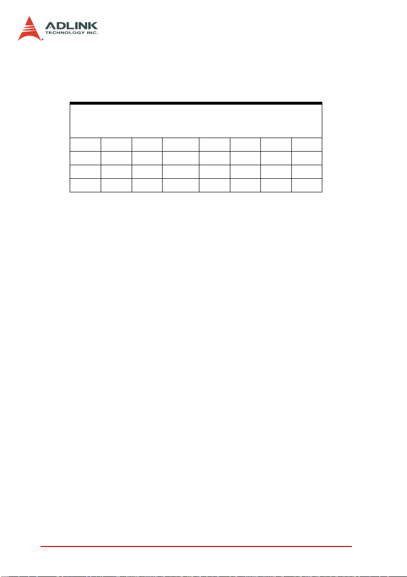
1: Function is enabled
0: Function is disabled
Address: BASE+0x3Ah
Reset Value: 0x0000h
Read/Write: R
ARDYS SRDYS RBRDYS SOES WIS WDTES HRHES
--
Bit7 Bit6 Bit5 Bit4 Bit3 Bit2 Bit1 Bit0
-- -- -- -- -- -- -- --
Bit15 Bit14 Bit13 Bit12 Bit11 Bit10 Bit9 Bit8
Bit15 - 7 Not used
Bit6 ARDYS: Flash Data Read/Write Finished Status
1: Process is not finished.
0: Process is finished.
Bit5 SRDYS: DO Data Sending Finishes Status
1: Process is not finished.
0: Process is finished.
Bit4 RBRDYS: DO Read Back Data Ready Status
1: DO read back data is not ready.
0: DO read back data is ready.
Bit3 SOES: Safety Out Enable Status
1: Function is enabled.
0: Function is disabled.
Bit2 WIS: WDT Interrupt Status
1: The WDT interrupt has asserted.
0: The WDT interrupt did not assert.
Bit1 WDTES: WDT Interrupt Enable Status
1: Function is enabled.
0: Function is disabled.
Bit0 HRHES: Hot Reset Hold Enable Status
1: Function is disabled.
0: Function is enabled.
64 Register Format
Page 77

TTL IO Setup, Status, DO and DI Registers
The PCI-7444 provides an extra 32-CH TTL I/O function for
optional applications. These TTL I/O channels are divided into two
16-bit banks. These channels are divided between two connectors: JP3 and JP4. You can choose the direction of each TTL
channel any time by setting up the two-bank TTL IO setup register.
Address R/W Value Mapping (MSB----LSB)
BASE+0x3C W TTL_IO_SETUP[15…0]
BASE+0x3E W TTL_IO_SETUP[31...16]
Bit value: 0: I/O direction is input. (Default)
1: I/O direction is output.
When you set up the direction of TTL I/O channels, the statuses of
setting can be read back through TTL IO S t a tus Read Back Regi sters. You can read back the I/O direction statuses to check if the
directions meet your need.
Address R/W Value Mapping (MSB----LSB)
BASE+0x3C R TTL_IO_STATUS[15…0]
BASE+0x3E R TTL_IO_STATUS[31...16]
Bit value: 0: I/O direction is input. (Default)
1: I/O direction is output.
When the I/O direction setting is output, you can send out data
through the TTL I/O output channel.
Address R/W Value Mapping (MSB----LSB)
BASE+0x40 W TTL_IO_DO[15…0]
BASE+0x42 W TTL_IO_DO[31...16]
Bit value: 0: Output in low logic. (Default)
1: Output in high logic.
Register Format 65
Page 78

When the I/O direction setting is input, you can read data throu gh
the TTL I/O input channel.
Address R/W Value Mapping (MSB----LSB)
BASE+0x40 R TTL_IO_DI[15…0]
BASE+0x42 R TTL_IO_DI[31...16]
Bit value: 0: Input in low logic.
1: Input in high logic. (Default)
66 Register Format
Page 79

4.4 Handling PCI Controller Registers
The PCI-7442/7443/7444 card adopts the PLX PCI-9030 PCI bus
controller. You should notice some registers when you attempt to
handle the card via low-level programming. The interrupt control
register (INTCSR; 0x4Ch) of PCI-9030 takes charge of all interrupt
information from local bus to PCI bus. When you want to develop
your own interrupt function driver, both interrupt registers in PCI9030 and in the PCI-7442/7443/7444 card have to work together.
For detailed information about the interrupt control register in PCI9030, refer to the PCI-9030 databook.
The PCI-7442/7443/7444 card’s function library provides simple
and easy-to-use functions that handle interrupt procedures. These
functions eliminate the handling of the interrupt register in the PCI
controller. It is recommended that you use these functions instead
of developing your own interrupt functions.
Register Format 67
Page 80

68 Register Format
Page 81

Warranty Policy
Thank you for choosing ADLINK. To understand your rights and
enjoy all the after-sales services we offer, please read the following carefully.
1. Before using ADLINK’s products please read the user manual and follow the instructions exactly. When sending in
damaged products for repair, please attach an RMA application form which can be downloaded from: http://
rma.adlinktech.com/policy/.
2. All ADLINK products come with a limited two-year warranty, one year for products bought in China:
X The warranty period starts on the day the product is
shipped from ADLINK’s factory.
X Peripherals and third-party products not ma nufactured
by ADLINK will be covered by the original manufacturers' warranty.
X For products containing storage devices (har d drive s,
flash cards, etc.), please back up your data before sending them for repair. ADLINK is not responsible for any
loss of data.
X Please ensure the use of properly licensed software with
our systems. ADLINK does not condone the use of
pirated software and will not service systems using such
software. ADLINK will not be held legally responsible for
products shipped with unlicensed software installed by
the user.
X For general repairs, please do not include peripheral
accessories. If peripherals need to be included, be certain to specify which items you sent on the RMA Request
& Confirmation Form. ADLINK is not responsible for
items not listed on the RMA Request & Confirmation
Form.
Warranty Policy 69
Page 82

3. Our repair service is not covere d by ADLI NK's guaran tee
in the following situations:
X Damage caused by not following instructions in the
User's Manual.
X Damage caused by carelessness on the user's part dur-
ing product transportation.
X Damage caused by fire, earthquak es, floods, lightening,
pollution, other acts of God, and/or incorrect usage of
voltage transformers.
X Damage caused by unsuitable storage environments
(i.e. high temperatures, high humidity, or volatile chemicals).
X Damage caused by leakage of battery fluid during or
after change of batteries by customer/user.
X Damage from improper repair by unauthorized ADLINK
technicians.
X Products with altered and/or damaged serial numbers
are not entitled to our service.
X This warranty is not transferable or extendible.
X Other categories not protected under our warranty.
4. Customers are responsible for shipping costs to transport
damaged products to our company or sales office.
5. To ensure the speed and quality of product repair, please
download an RMA application form from our company website: http://rma.adlinktech.com/policy. Damaged products
with attached RMA forms receive priority.
If you have any further questions, please email our FAE staff:
service@adlinktech.com.
70 Warranty Policy
 Loading...