

Page 1
HPERC-IBR-MC/MH
High Performance Extreme Rugged™ Computer System
User’s Manual
Manual Rev.: 0.20 Preliminary
Revision Date: May 5, 2015
Part No: 50-1Z178-1000
Advance Technologies. Automate the World.
Page 2

Revision History
Revision Reason for Change Date
0.10 Preliminary draft 13-01-2015
0.20 Minor corrections 05-05-2015
ii Revision History
Page 3

HPERC-IBR-M
Preface
© Copyright 2015 ADLINK Technology, Inc.
www.adlinktech.com
Disclaimer
Information in this document is provided in connection with ADLINK products. No license,
express or implied, by estoppel or otherwise, to any intellectual property rights is granted by this
document. Except as provided in ADLINK´s Terms and Conditions of Sale for such products,
ADLINK assumes no liability whatsoever, and ADLINK disclaims any express or implied warranty, relating to sale and/or use of ADLINK products including liability or warranties relating to
fitness for a particular purpose, merchantability, or infringement of any patent, copyright or other
intellectual property right. If you intend to use ADLINK products in or as medical devices, you
are solely responsible for all required regulatory compliance, including, without limitation, Title
21 of the CFR (US), Directive 2007/47/EC (EU), and ISO 13485 & 14971, if any. ADLINK may
make changes to specifications and product descriptions at any time, without notice.
Trademarks
MS-DOS, Windows, Windows 95, Windows 98, Windows NT and Windows XP are trademarks of Microsoft Corporation. PS/2 is a trademark of International Business Machines, Inc.
Intel and Solid State Drive are trademarks of Intel Corporation. PC/104 is a registered trademark of the PC/104 Consortium. CoreModule is a registered trademark, and ADLINK, Little
Board, LittleBoard, MightyBoard, MightySystem, MilSystem, MiniModule, ReadyBoard,
ReadyBox, ReadyPanel, RuffSystem, ReadySystem, and HPERC are trademarks of
ADLINK Technology, Inc. All other marks are the properties of their respective companies.
Audience
This manual provides reference only for computer design engineers, including but not limited
to hardware and software designers and applications engineers. ADLINK Technology, Inc.
assumes you are qualified to design and implement prototype computer equipment.
Preface iii
Page 4

This page intentionally left blank.
iv Preface
Page 5

HPERC-IBR-M
Table of Contents
Revision History................................................................................................................... ii
Preface................................................................................................................................. iii
List of Figures .................................................................................................................... vii
List of Tables....................................................................................................................... ix
1 HPERC-IBR-M Setup ........................................................................................................1
1.1 About the HPERC-IBR-M....................................................................................................... 1
1.2 Using this Guide..................................................................................................................... 1
1.3 Requirements......................................................................................................................... 1
1.4 Device/Peripheral Connections.............................................................................................. 1
1.5 Power Specifications............................ .... .......................................... ... ... ... .... ... ... ... ... .... ....... 2
1.6 Environmental Specifications................................................................................................. 3
1.7 What’s in the Box.... .... ... ... ... .... .......................................... ... ... .............................................. 4
1.8 Setup Steps ........................................................................................................................... 5
1.9 Setting Up the Work Space ................................................................................................... 5
1.10 Installing Mounting Screws.................................................................................................... 6
1.11 Connecting Peripherals.......................................................................................................... 8
1.12 P2 and P3 Military Connector........................................ .... ... ... ... ... ...................................... 10
1.12.1P2 Pin Definit ions ..................................... ... .... ... ... ... .......................................... ... .... ......11
1.12.2P3 Pin Definit ions ..................................... ... .... ... ... ... .......................................... ... .... ......14
1.13 Applying Power to the HPERC-IBR-M................................................................................. 19
2 Internal Components......................................................................................................21
2.1 HPERC-IBR-M Assembly Procedures................................................................................. 21
2.1.1 Tools Required ................................................................................................................21
2.1.2 Shutting Down the HPERC-IBR-M ..................................................................................21
2.1.3 Replacing the SSDs (Solid State Drives).........................................................................22
2.1.4 Replacing the SD (Secure Digital) Memory Card ............................................................23
2.1.5 Removing and installing the system cover plate on the HPERC-IBR-M enclosure.........24
2.1.6 Replacing the PCI/104-Express expansion module ........................................................25
2.1.7 Replacing the SODIMM memory........................................................ ... .... ... ... ... ... .... ...... 27
2.1.8 Replacing the Mini PCIe Card .........................................................................................30
Appendix A Sample Code............................................................................................... 31
Getting Service................................................................................................................... 33
v
Page 6

This page intentionally left blank.
vi
Page 7

HPERC-IBR-M
List of Figures
Figure 1-1: i7-3517UE Peak In-Rush Current and Duration...............................................................2
Figure 1-2: HPERC-IBR-M Unit with Accessories..............................................................................4
Figure 1-3: Top and Front Views of “MH” Enclosure with Mounting Dimensions ...............................6
Figure 1-4: Top and Front Views of “MC” Enclosure with Mounting Dimensions ...............................7
Figure 1-5: Front View of HPERC-IBR-M I/O Panel...........................................................................8
Figure 1-6: P2 and P3 Military Interface Connector Pin Locations...................................................10
Figure 2-7: Exploded View of HPERC-IBR-M with SSDs.................................................................22
Figure 2-8: Exploded View of HPERC-IBR-M with SD Card ............................................................23
Figure 2-9: Exploded View of HPERC-IBR-M with System Cover Plate and Screws ......................24
Figure 2-10: Exploded View of HPERC-IBR-M with SSD Bracket and Screws..................................25
Figure 2-11: Exploded View of HPERC-IBR-M with PCI/104-Express Module and Screws ..............26
Figure 2-12: Top View of HPERC-IBR-M with Open Enclosure and Flexible Printed Circuit Screws 27
Figure 2-13: Exploded View of HPERC-IBR-M with Flexible Printed Circuit Connector ....................28
Figure 2-14: Exploded View of HPERC-IBR-M with interface board..................................................28
Figure 2-15: Exploded View of HPERC-IBR-M with SODIMM and Cover Plate ................................29
Figure 2-16: Top View of HPERC-IBR-M with Open Enclosure and Mini PCIe Card.........................30
List of Figures vii
Page 8

This page intentionally left blank.
viii List of Figures
Page 9

HPERC-IBR-M
List of Tables
Table 1-1: System Power Requirements ............................................................................................2
Table 1-2: Environmental Requirements .......................................................................... ... ...............3
Table 1-3: I/O Panel Connectors (Refer to Figure 1-5 for connector locations.).................................9
Table 1-4: P2 Military Connector Signals..........................................................................................11
Table 1-5: P3 Connector Pin Signals................................................................................................14
List of Tables ix
Page 10

This page intentionally left blank.
x List of Tables
Page 11

HPERC-IBR-M
1 HPERC-IBR-M Setup
1.1 About the HPERC-IBR-M
The HPERC products are intended for users of embedded systems requiring long life-cycles,
configuration control, and ruggedness in hardened military packages. HPERC models feature
Extreme Rugged™ computer boards available with varieties of processors and memory. An
optional operating system (OS) can be pre-loaded onto an optional internal storage device (two
2 ½" Solid State Drives (SSDs). Board Support Packages (BSPs) are provided on the optional
Support Software QuickDrive™ to support addition al OSs. Just use a USB memory to load your
application software and you are ready to use your system.
1.2 Using this Guide
This guide provides the most efficient way to set up your HPERC-IBR-M with your desired OS.
The instructions provided in this guide include:
X Removing the HPERC-IBR-M from the shipping container and inspecting the accesso-
ries
X Connecting peripherals to the HPERC-IBR-M
X Powering up the HPERC-IBR-M
X Opening the HPERC-IBR-M
X Replacing internal components
Information not provided in this User’s Guide includes:
X Board or Module specifications
X Board or Module header signals and descriptions
X Operating system programming or operating instructions
NOTE: Refer to OS manufacturers’ manuals for instructions when using OS software.
1.3 Requirements
The following peripherals and devices are needed to make full use of the HPERC-IBR-M.
X Peripherals (user-provided):
Z USB or PS/2 keyboard
Z USB or PS/2 mouse
Z Display monitor
NOTE: The items listed above are not available from ADLINK.
X Power Supply (optional):
Z AC Adapter (with plug-type mating cord)
1.4 Device/Peripheral Connections
X Ethernet (LAN) connections
X USB device connections
X At least one PCIe/104-Express expansion module
1
Page 12
1.5 Power Specifications
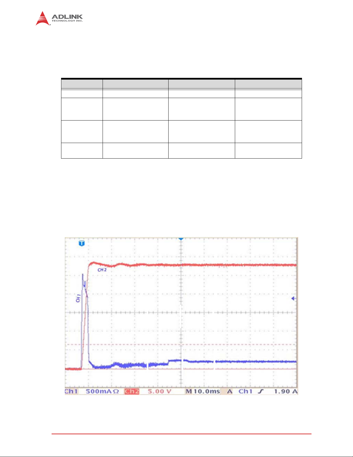
Table 1-1 defines the current draw values of the HPERC-IBR-M, featuring either the 3517UE,
3555LE, or 3612QE i7 CPUs. The table captures In-Rush, Idle, and Burn-In-Test (BIT) currents
at +28V input voltage.
Table 1-1 lists the current draw values of the HPERC-IBR-M
Parameter 1.7GHz CPU (i7-3517UE) 2.5GHz CPU (i7-3555LE) 2.1GHz CPU (i7-3612QE)
Input Type
In-Rush Peak
Current and
Duration
Idle Current and
Power
(Windows 7)
BIT Current and
Power
Operating configurations:
X In-rush operating configuration includes one VGA monitor and 4GB DDR3-1333L RAM.
X Idle operating configuration includes the In-rush configurat ion as well as one SATA 3.5"
HDD with Windows XP and one USB keyboard and mouse.
X BIT (Burn-In-Test) operating configuration is the same as the Idle configuration
+28 VDC Regulated DC +28 VDC Regulated DC +28 VDC Regulated DC
See Figure 1-1 Not yet measured Not yet measured
0.79A (22.22W) Not yet measured Not yet measured
1.18A (32.96W) Not yet measured Not yet measured
Table 1-1: System Power Requirements
Figure 1-1: i7-3517UE Peak In-Rush Current and Duration
2
Page 13
HPERC-IBR-M
1.6 Environmental Specifications
Table 1-2 provides the most efficient operating and storage condition ranges required for this
system.
NOTE: Extended temperature range available only on extended temperature tested (ETT)
systems.
Temperature Humidity
Standard Storage Extended Operating Non-operating
-20° to +65°C
(-4° to +149°F)
–55° to +85°C
(–67° to +185°F)
T able 1-2: Environmental Requirements
–40° to +75°C
(–40° to +167°F)
5% to 90%
relative humidity,
non-condensing
5% to 95%
relative humidity ,
non-condensing
3
Page 14

1.7 What’s in the Box
The Contents List identifies the items in the shipping box for the HPERC-IBR-M Unit and
HPERC-IBR-M Accessories (sold separately.) See Figure 1-2.
HPERC-MH
Cooling Fins
(pre-installed on
MH version only)
HPERC-MC
Cold Plate
(pre-installed on
MC version, only)
Breakout
Cables
HPERC Accessories (sold separately)
SATA
DC Cable
Connector
Breakout
Cables
Support
Software
QuickDrive
Mounting Flanges
(pre-installed)
AC Adapter
Mating
AC
Cable
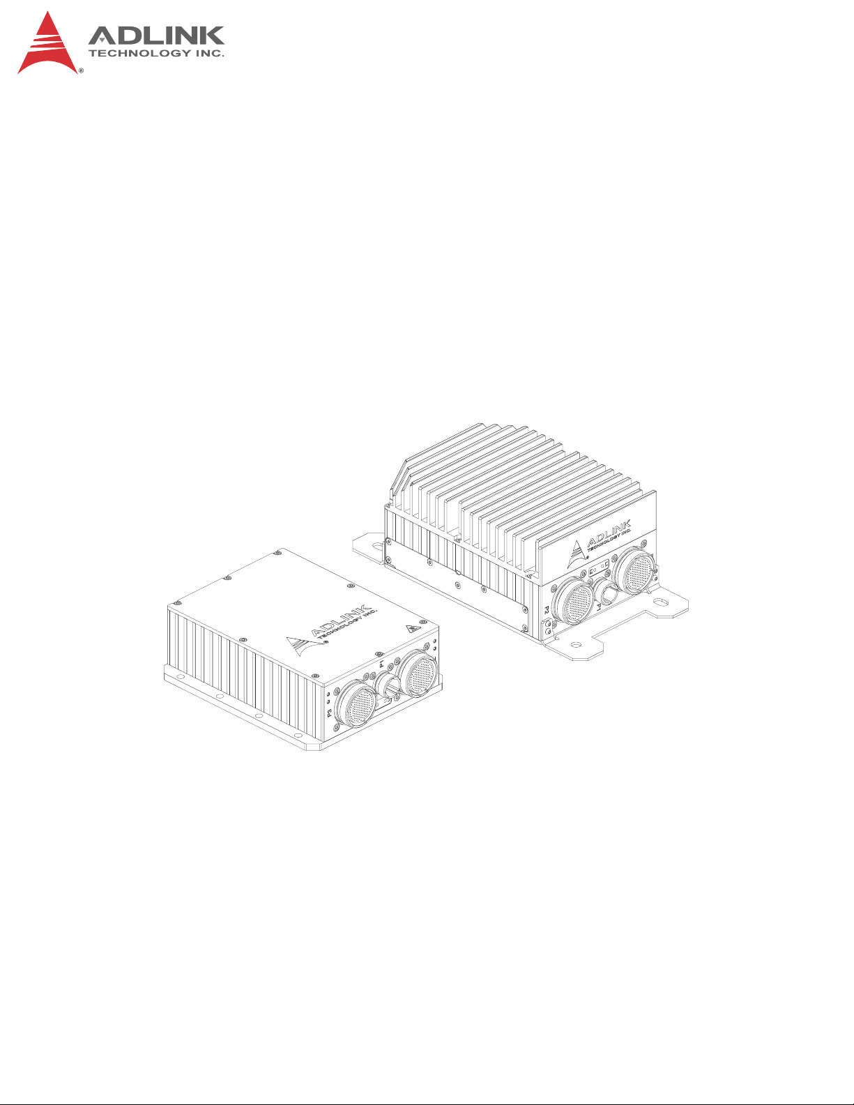
Figure 1-2: HPERC-IBR-M Unit with Accessories
4
Page 15

HPERC-IBR-M
1.8 Setup Steps
Follow the setup steps in this section in the order listed. Skip any step s th at do not app ly to your
application.
1) Open shipping box.
2) Verify contents.
• Locate the HPERC-IBR-M Contents List.
• Unpack the contents of the shipping box.
• V erify the contents of the shipping box against the Contents List included with
your HPERC-IBR-M.
• If anything is missing or damaged, call your sales representative. Refer to the
ADLINK web page at http://www.adlinktech.com
for contact information.
1.9 Setting Up the Work Space
CAUTION: T o prevent damage to the HPERC-IBR-M, ensure sufficient clearance exists
around the cooling solution for unrestricted airflow.
The air temperature inside the enclosure could rise above the specified operating temperature
limits if the airflow through the cooling solutionis restricted.
3) Select workbench
location.
4) Unpack
HPERC-IBR-M.
• The workbench location should be a flat clean surface for setup and operation
(including the connection of any external peripherals and optional devices).
• Ensure sufficient airflow clearance exists around the complete enclosure.
• Remove the HPERC-IBR-M from its shipping container and place it on a flat
work surface.
• The HPERC-IBR-M enclosure combined with CPU, storage (SSD), and the
desired OS form a complete system, ready for operation.
5
Page 16

1.10 Installing Mounting Screws
5) Install mounting
screws.
• Install mounting screws (not included) for surface or wall mounting to the
mounting flanges of the HPERC-IBR-M. See Figure 1-3 and Figure1-4.
Mounting Screws =
3/8
" - 16 (M10x1.5)
Figure 1-3: Top and Front Views of “MH” Enclosure with Mounting Dimensions
6
Page 17

HPERC-IBR-M
Mounting Screws =
" - 20 (M6x1)
1/4
Figure 1-4: Top and Front Views of “MC” Enclosure with Mounting Dimensions
7
Page 18

1.11 Connecting Peripherals
6) Connect the
appropriate military
breakout cable to the
corresponding
HPERC-IBR-M military
connector. See
Figure 1-2 for
illustrations of cables.
See Figure 1-5 for
locations of the
HPERC-IBR-M military
connectors.
• Refer to Figure1-5 for locations and descriptions of the connectors before
making connections or powering on the HPERC-IBR-M.
• Connect the USB or PS2 keyboard to the corresponding connector on the
appropriate breakout cable.
• Connect the USB or PS2 mouse to the appropriate connector on the
corresponding breakout cable.
• Connect the VGA or LCD displayto the appropriate connector on the
corresponding breakout cable.
HPERC-IBR-MH
P2 Military
Connector
HPERC-IBR-MC
Figure 1-5: Front View of HPERC-IBR-M I/O Panel
8
P1 DC
Power In
P3 Military
Connector
Page 19

HPERC-IBR-M
G
G
Control/Connector Description
P1 DC Power In This Military Power connector accepts DC voltages from an external
GND
ND
A
D
GND
ND
V+
V+
B
C
HPERC_DC_In_Pinout_b
V+
source.
NOTE: This connector is manufactured by Amphenol.
P2 Military Connector This military connector provides signals for Ethernet Ports, USB 2.0,
Serial Ports, Reset Switch, Ethernet LEDs, and UNDIO.
P3 Military Connector This military connector provides signals for VGA, Ethernet LEDs,
Ethernet Ports, Serial Ports, PS/2 Keyboard and Mouse, and RCA
Jack.
Table 1-3: I/O Panel Connectors (Refer to Figure 1-5 for connector locations.)
NOTE: T o connect an external Hard Disk Drive (HDD) or CD-ROM to the HPERC-IBR-M,
use one of the USB or SATA ports to connect the device.
9
Page 20

1.12 P2 and P3 Military Connector
The following two tables define the signals and signal maps of the two military I/O connectors
(P2 and P3) on the HPERC-IBR-M. Each table lists the P2 or P3 p in nu mbers, th e sign al names
and descriptionsand the corresponding pins of the internal IO boards (HIBR and Interface
Board.) Figure 1-6 provides the number and location of each pin on the two military connectors.
HPERC_J2J3_connPins_b
10
Figure 1-6: P2 and P3 Military Interface Connector Pin Locations
Page 21

1.12.1 P2 Pin Definitions
Table 1-4 Provides the pin definitions and signal maps for the P3 Military Connector.
HPERC-IBR-M
P2
Pin
Interface Signal Signal Description
HIBR
Pin
Interface
Board Pin
1 Gigabit Ethernet 1 GbE2_MDI0_P Ethernet1 MDI0 Positive 138 CN2-25
2 Gigabit Ethernet 1 GbE2_MDI1_N Ethernet1 MDI1 Negative 127 CN2-59
3 Gigabit Ethernet 1 GbE2_MDI1_P Ethernet1 MDI1 Positive 137 CN2-58
4 Ground GND Ground 175 NA
5 Gigabit Ethernet 1 GbE2_MDI2_N Ethernet1 MDI2 Negative 98 CN2-50
6 Gigabit Ethernet 1 GbE2_MDI2_P Ethernet1 MDI2 Positive 108 CN2-49
7 Gigabit Ethernet 1 GbE2_MDI3_N Ethernet1 MDI3 Negative 97 CN2-53
8 Gigabit Ethernet 1 GbE2_MDI0_N Ethernet1 MDI0 Negative 128 CN2-26
14 Gigabit Ethernet 1 GbE2_MDI3_P Ethernet1 MDI3 Positive 107 CN2-52
9 USB 2.0, Port 4 USB_P4 Data Positive 351 CN2-28
10 USB 2.0, Port 4 USB_N4 Data Negative 361 CN2-29
1 1 USB 2.0, Port 4 USB_GND4 Ground 205 NA
12 USB 2.0, Port 5 USB_P5 Data Positive 321 CN2-31
13 USB 2.0, Port 5 USB_N5 Data Negative 331 CN2-32
27 USB 2.0, Port 5 USB_GND5 Ground 235 NA
15 USB 2.0, Port 4 P5V_USB4 +5 Volts Power NA NA
16 USB 2.0, Port 5 P5V_USB5 +5 Volts Power NA NA
17 Serial 4 RS422_TX4_N Transmit Data Negative 381 CN1-46
18 Serial 4 RS422_TX4_P Transmit Data Positive 391 CN1-45
19 Serial 4 RS422_RX4_N Receive Data Negative 382 CN1-48
20 Serial 4 RS422_RX4_P Receive Data Positive 392 CN1-47
21 Serial 6 RS422_RX6_N Receive Data Negative 130 CN1-23
22 Serial 6 RS422_RX6_P Receive Data Positive 140 CN1-22
23 Serial 6 RS422_TX6_N Transmit Data Negative 100 CN1-21
24 Serial 6 RS422_TX6_P Transmit Data Positive 1 10 CN1-20
25 Power P5V +5 Volts Power 306 NA
26 Power P5V +5 Volts Power 316 NA
27 Ground GND Ground NA NA
28 USB 2.0, Port 8 USB_PWR8 USB 2.0 +5V Power NA NA
30 USB 2.0, Port 8 USB_P8 USB 2.0 Data Positive 353 CN2-34
31 USB 2.0, Port 8 USB_N8 USB 2.0 Data Negative 363 CN2-35
32 USB 2.0, Port 8 USB_GND8 USB 2.0 Ground 285 NA
29 Reset Switch RESET#_HDR Resets the system 265 CN4-4
38 Ground GND Ground 335 NA
33 Control/Indicator PWR_LED Power LED (330ohm to
NA NA
+5V)
44 Ground GND Ground 6 NA
34 Control/Indicator PCIe_ETH_2/5_LED1 Ethernet LED 35 CN1-44
44 Ground GND Ground 6 NA
35 NC NC Not Connected NA NA
Table 1-4: P2 Military Connector Signals
11
Page 22

P2
Pin
Interface Signal Signal Description
HIBR
Pin
Interface
Board Pin
44 Ground GND Ground 6 NA
36 Control/Indicator HPOUT_R Audio Right NA NA
37 Control/Indicator HPOUT_L Audio Left NA NA
38 Ground GND Ground 335 NA
39 Power PV5 +5 Volts Power 326 NA
40 Power PV5 +5 Volts Power 307 NA
38 Ground GND Ground 335 NA
41 Ground GND Ground 375 NA
42 User Defined IO UDNI O1 1 User Input/Output Port 11 NA CN4-15
43 User Defined IO UDNI O12 User Input/Output Port 12 NA CN4-16
38 Ground GND Ground 335 NA
44 Ground GND Ground 6 NA
45 User Defined IO UDNI O13 User Input/Output Port 13 NA CN4-17
46 User Defined IO UDNI O14 User Input/Output Port 14 NA CN4-18
38 Ground GND Ground 335 NA
47 Ground GND Ground 16 NA
48 User Defined IO UDNI O15 User Input/Output Port 15 NA CN4-19
49 User Defined IO UDNI O16 User Input/Output Port 16 NA CN4-20
50 Ground GND Ground 46 NA
51 User Defined IO UDNI O17 User Input/Output Port 17 NA CN4-21
52 User Defined IO UDNI O18 User Input/Output Port 18 NA CN4-22
53 Ground GND Ground 76 NA
54 User Defined IO UDNI O19 User Input/Output Port 19 NA CN4-23
55 User Defined IO UDNI O20 User Input/Output Port 20 NA CN4-24
56 Ground GND Ground 106 NA
57-81 NC NA NA NA NA
71 User Defined IO UDNIO5 User Input/Output Port 5 NA CN4-9
72 User Defined IO UDNIO6 User Input/Output Port 6 NA CN4-10
73 Ground GND Ground 57 NA
74 User Defined IO UDNIO7 User Input/Output Port 7 NA CN4-1 1
75 User Defined IO UDNIO8 User Input/Output Port 8 NA CN4-12
76 Ground GND Ground 87 NA
77 User Defined IO UDNIO9 User Input/Output Port 9 NA CN4-13
78 User Defined IO UDNIO10 User Input/Output Port 10 NA CN4-14
79 Ground GND Ground 1 17 NA
82 Control/Indicator LINE_IN_R Audio In Right Channel NA NA
83 Control/Indicator LINE_IN_L Audio In Left Channel NA NA
84 NC NC NC NA
85 Ground AGND Analog Ground NA NA
86 Ground AGND Analog Ground NA NA
87 Ground GND Ground 366 NA
88 User Defined IO UDNIO1 User Input/Output Port 1 NA CN4-5
Table 1-4: P2 Military Connector Signals (Continued)
12
Page 23

HPERC-IBR-M
P2
Pin
Interface Signal Signal Description
HIBR
Pin
Interface
Board Pin
89 User Defined IO UDNIO2 User Input/Output Port 2 NA CN4-6
90 Ground GND Ground 376 NA
91 User Defined IO UDNIO3 User Input/Output Port 3 NA CN4-7
92 User Defined IO UDNIO4 User Input/Output Port 4 NA CN4-8
93 Ground GND Ground 27 NA
94 Power P3V3_S +3.3 Volt s St andby NA NA
95 Power P3V3_S +3.3 Volt s St andby NA NA
96 Ground GND Ground 256 NA
98 Power Switch PWERBTN_H DR Powers on the system 348 NA
97 USB 2.0, Port 9 USB_PWR9 USB 2.0 +5V Power NA NA
99 USB 2.0, Port 9 USB_N9 USB 2.0 Data Negative 396 CN2-37
100 USB 2.0, Port 9 USB_P9 USB 2.0 Data Positive 386 CN2-38
101 Ground GND Ground 286 NA
102 Control/Indicator SA T A_LED# SA TA LED 1 19 CN4-1
101 Ground GND Ground 286 NA
103 NC NC NC
101 Ground GND Ground 286 NA
104 Control/Indicator ERASE- L GPIO Signal for SSD
109 CN4-2
Secure Erase
101 Ground GND Ground 286 NA
105 Power P3V3_S +3.3 Volts S tandby NA NA
106 Power P3V3_S +3.3 Volts S tandby NA NA
107 Serial 5 RS422_TX5_N Transmit Data Negative 160 CN1-31
108 Serial 5 RS422_TX5_P Transmit Data Positive 170 CN1-30
109 Serial 5 RS422_RX5_N Receive Data Negative 157 CN1-33
1 10 Serial 5 RS422_RX5_P Receive Data Positive 167 CN1-32
1 1 1 Serial 7 RS422_TX7_N Transmit Data Negative 242 CN1-36
1 12 Serial 7 RS422_TX7_P Transmit Data Positive 252 CN1-35
1 13 Serial 7 RS422_RX7_N Receive Data Negative 243 CN1-38
1 14 Serial 7 RS422_RX7_P Receive Data Positive 253 CN1-37
116-
NC NA NA NA NA
120
1 15 Serial 0 RS422_TX0_N Transmit Data Negative 159 CN1-26
122 Serial 0 RS422_TX0_P Transmit Data Positive 169 CN1-25
123 Serial 0 RS422_RX0_N Receive Data Negative 168 CN1-28
124 Serial 0 RS422_RX0_P Receive Data Positive 158 CN1-27
125 Ground GND Ground 196 NA
126 Serial 2 RS422_TX2_N Transmit Data Negative 301 CN1-41
127 Serial 2 RS422_TX2_P Transmit Data Positive 291 CN1-40
128 Serial 2 RS422_RX2_N Receive Data Negative 271 CN1-43
121 Serial 2 RS422_RX2_P Receive Data Positive 261 CN1-42
Table 1-4: P2 Military Connector Signals (Continued)
13
Page 24

1.12.2 P3 Pin Definitions
Table 1-5 Provides the pin definitions and signal maps for the P3 Military Connector.
Pin
Interface
Board
Pin
P3
Pin
Interface Signal Signal Description
HIBR
1 VGA VGA_VSYNC Vertical Sync 40 CN1-1 1
2 Ground GND Ground 207 NA
33 Ground GND Ground 8 NA
3 VGA VGA_DDC_SCL Display Data Channel -
10 CN1-7
Serial Clock
4 VGA VGA_DDC_SDA Display Data Channel -
20 CN1-8
Serial Data
5 Ground GND Ground 237 NA
6 VGA RED Red Analog Output 29 CN1-5
18 Ground GND Ground 297 NA
7 VGA GREEN Green Analog Output 19 CN1-3
21 Ground GND Ground 347 NA
14 VGA BLUE Blue Analog Output 9 CN1-1
30 Ground GND Ground 367 NA
8 VGA HSYNC Horizontal Sync 30 CN1-10
9 Power P3V3_S +3.3 Volts St andby NA NA
10 Power P3V3_S +3.3 Volts S tandby NA NA
1 1 Ground GND Ground 267 NA
12 Power P3V3_S +3.3 Volts S tandby NA NA
13 Power P3V3_S +3.3 Volts S tandby NA NA
15 Power P3V3_S +3.3 Volts S tandby NA NA
38 Ground GND Ground 38 NA
24 Control/Indicator PCIe_ETH_5/5_LED1 Ethernet LED 164 CN1-58
99 Ground GND Ground 99 NA
1 14 Control/Indicator PCIe_ETH_4/5_LED1 Ethernet LED 174 CN1-55
99 Ground GND Ground 99 NA
121 Control/Indicator PCIe_ETH_3/5_LED1 Ethernet LED 32 CN1-49
99 Ground GND Ground 99 NA
16 Gigabit Ethernet 4 GbE5_MDI0_N Ethernet4 MDI0
185 CN2-56
Negative
17 Gigabit Ethernet 4 GbE5_MDI0_P Ethernet4 MDI0 Positive 195 CN2-55
18 Ground GND Ground 347 NA
19 Gigabit Ethernet 4 GbE5_MDI1_N Ethernet4 MDI1
75 CN2-41
Negative
20 Gigabit Ethernet 4 GbE5_MDI1_P Ethernet4 MDI1 Positive 65 CN2-40
21 Ground GND Ground 347 NA
22 Gigabit Ethernet 4 GbE5_MDI2_N Ethernet4 MDI2
74 CN2-44
Negative
23 Gigabit Ethernet 4 GbE5_MDI2_P Ethernet4 MDI2 Positive 64 CN2-43
T able 1-5: P3 Connector Pin Signals
14
Page 25

HPERC-IBR-M
Pin
Interface
Board
Pin
P3
Pin
Interface Signal Signal Description
100 Gigabit Ethernet 4 GbE5_MDI3_N Ethernet4 MDI3
HIBR
155 CN2-47
Negative
101 Gigabit Ethernet 4 GbE5_MDI3_P Ethernet4 MDI3 Positive 165 CN2-46
25 Serial 1 RS422_TX1_N Transmit Data Negative 28 CN1-16
26 Serial 1 RS422_TX1_P Transmit Data Positive 18 CN1-15
27 Serial 1 RS422_RX1_N Receive Data Negative 161 CN1-18
28 Serial 1 RS422_RX1_P Receive Data Positive 151 CN1-17
29 NC NA NA NA NA
108 Ground GND Ground 39 NA
36 Gigabit Ethernet 2 GbE3_MDI2_N Ethernet2 Negative 134 CN2-8
37 Gigabit Ethernet 2 GbE3_MDI2_P Ethernet2 Positive 124 CN2-7
38 Ground GND Ground 58 NA
39 Gigabit Ethernet 2 GbE3_MDI3_N Ethernet3 Negative 135 CN2-11
40 Gigabit Ethernet 2 GbE3_MDI3_P Ethernet3 Positive 125 CN2-10
41 NA GND Ground 58 NA
42 Gigabit Ethernet 2 GbE3_MDI1_N Ethernet1 Negative 95 CN2-5
43 Gigabit Ethernet 2 GbE3_MDI1_P Ethernet1 Positive 105 CN2-4
44 Ground GND Ground 88 NA
45 Gigabit Ethernet 2 GbE3_MDI0_N Ethernet0 Negative 104 CN2-2
46 Gigabit Ethernet 2 GbE3_MDI0_P Ethernet0 Positive 94 CN2-1
47 Ground GND Ground 1 18 NA
48 DVI 1 DDIB_P2 Digital Display Interface
91 CN3-27
Port B, TMDS Data 0
Positive
49 DVI 1 DDIB_N2 Digital Display Interface
101 CN3-31
Port B, TMDS Data 0
Negative
50 Ground GND Ground 148 NA
51 DVI 1 DDIB_P1 Digital Display Interface
41 CN3-15
Port B, TMDS Data 1
Positive
52 DVI 1 DDIB_N1 Digital Display Interface
31 CN3-19
Port B, TMDS Data 1
Negative
53 Ground GND Ground 178 NA
54 DVI 1 DDIB_P0 Digital Display Interface
71 CN3-3
Port B, TMDS Data 2
Positive
55 DVI 1 DDIB_N0 Digital Display Interface
61 CN3-7
Port B, TMDS Data 2
Negative
56 Ground GND Ground 208 NA
Table 1-5: P3 Connector Pin Signals (Continued)
15
Page 26

P3
Pin
Interface Signal Signal Description
57 DVI 1 DDIB_P3 Digital Display Interface
HIBR
121 CN3-73
Interface
Pin
Port B, TMDS Clock
Positive
58 DVI 1 DDIB_N3 Digital Display Interface
131 CN3-77
Port B, TMDS Clock
Negative
59 DVI 1 DDIB_CLK_AUXP Digital Display Interface
354 CN3-40
Port B, DDC Serial
Clock
60 DVI 1 DDIB_DAT_AUXN Digi tal Display Interface
374 CN3-44
Port B, DDC Serial Data
61 DVI 1 DDPB_HPD Digital Display Port B
364 CN3-48
Hot Plug Detect
94 DVI 1 DDPB_AUX_SEL Digital Display Port B
12 CN3-60
Auxiliary Select
62 DVI 2 DDIC_CLK_AUXP Digital Display Interface
365 CN3-16
Port C, DDC Serial
Clock
63 DVI 2 DDIC_DAT_AUXN Digital Display Interface
345 CN3-20
Port C, DDC Serial Data
64 DVI 2 DDPC_HPD Digital Display Port C
355 CN3-52
Hot Plug Detect
71 DVI 2 DDIC_P2 Digital Display Interface
1 CN3-1
Port C, TMDS Data 0
Positive
72 DVI 2 DDIC_N2 Digital Display Interface
1 1 CN3-5
Port C, TMDS Data 0
Negative
76 Ground GND Ground 50 NA
73 Ground GND Ground 379 NA
74 DVI 2 DDIC_P1 Digital Display Interface
5 CN3-74
Port C, TMDS Data 1
Positive
75 DVI 2 DDIC_N1 Digital Display Interface
15 CN3-78
Port C, TMDS Data 1
Negative
76 NC NA NA NA NA
77 DVI 2 DDIC_P0 Digital Display Interface
13 CN3-2
Port C, TMDS Data 2
Positive
78 DVI 2 DDIC_N0 Digital Display Interface
3 CN3-6
Port C, TMDS Data 2
Negative
76 Ground GND Ground 50 NA
79 Ground GND Ground 90 NA
Table 1-5: P3 Connector Pin Signals (Continued)
Board
Pin
16
Page 27

HPERC-IBR-M
P3
Pin
Interface Signal Signal Description
80 DVI 2 DDIC_P3 Digital Display Interface
HIBR
Interface
Pin
Board
Pin
7 CN3-72
Port C, TMDS Clock
Positive
81 DVI 2 DDIC_N3 Digital Display Interface
17 CN3-76
Port C, TMDS Clock
Negative
95 DVI 2 DDPC_AUX_SEL DisplayPort C Auxiliary
14 CN3-75
Select
65 PS/2 Mouse CLK_MS_CON Mouse Clock 279 CN1-56
66 PS/2 Mouse DA T_MS_CON Mouse Data 269 CN1-57
76 NC NA NA NA NA
67 PS/2 Keyboard CLK_KBD_CON Keyboard Clock 259 CN1-59
68 PS/2 Keyboard DA T_KBD_CON Keyboard Data 249 CN1-60
79 Ground GND Ground 90 NA
69 PS/2 Mouse Keyb oard POWER POWER NA NA
70 RCA Jack COMPOSITE_OUT Composite Out NA NA
82-84 NC NA NA NA NA
87-89 NC NA NA NA NA
103 USB 2.0, Port 2 USB_P2 USB 2.0 Data Positive,
322 CN3-25
TMDS_P2_SDA
104 USB 2.0, Port 2 USB_N2 USB 2.0 Data Negative,
332 CN3-29
TMDS_P2_SCL
125 USB 2.0, Port 2 P5V_USB2_P2 USB 2.0 +5VDC NA NA
126 NC NA NA NA NA
85-86,
NC NA NA NA NA
90-93
34 USB 2.0, Port 3 USB_P3 Data Positive, L VDS
352 CN3-61
Display Data Channel Data
35 USB 2.0, Port 3 USB_N3 Data Negative, L VDS
362 CN3-65
Display Data Channel Clock
127 USB 2.0, Port 3 P5V_USB2_P3 USB 2.0 +5VDC NA NA
128 NC NA NA NA NA
96 Power PV5 +5 Volts Power,
337 NA
DisplayPort D Auxiliary
Select
97 Power PV5 +5 Volts Power, High
338 NA
Definition Control Run
98 Power PV5 +5 Volts Power,
348 NA
PCIe_ETH_2/5_LED2
99 Ground GND Ground 99 NA
102 Ground GND Ground 129 NA
106 Gigabit Ethernet 3 GbE4_MDI1_N Ethernet1 Negative 156 CN2-20
Table 1-5: P3 Connector Pin Signals (Continued)
17
Page 28

Pin
Interface
Board
Pin
P3
Pin
Interface Signal Signal Description
HIBR
107 Gigabit Ethernet 3 GbE4_MDI1_P Ethernet1 Positive 146 CN2-19
109 Gigabit Ethernet 3 GbE4_MDI0_N Ethernet0 Negative 176 CN2-14
1 10 Gigabit Ethernet 3 GbE4_MDI0_P Ethernet0 Positive 186 CN2-13
1 1 1 Ground GND Ground 69 NA
1 12 Gigabit Ethernet 3 GbE4_MDI2_N Ethernet2 Negative 67 CN2-17
1 13 Gigabit Ethernet 3 GbE4_MDI2_P Ethernet2 Positive 77 CN2-16
30 Ground GND Ground 367 NA
31 Gigabit Ethernet 3 GbE4_MDI3_N Ethernet3 MDI3
68 CN2-23
Negative
32 Gigabit Ethernet 3 GbE4_MDI3_P Ethernet3 MDI3 Positive 78 CN2-22
1 15 Power PV5 +5 Volt s Power , TV
317 NA
OUT Color
122 Ground GND Ground 238 NA
123 Power PV5 +5 Volts Power , TV
327 NA
OUT Luminance)
124 Ground GND Ground 268 NA
116 NC NA NA NA NA
117 NC NA NA NA NA
118 NC NA NA NA NA
119 NC NA NA NA NA
120 NC NA NA NA NA
Table 1-5: P3 Connector Pin Signals (Continued)
18
Page 29

1.13 Applying Power to the HPERC-IBR-M
HPERC-IBR-M
7) Follow these steps to
apply power to the
HPERC-IBR-M.
8) Verify the HPERC-IBR-M
satisfactorily powers on.
• Connect the AC Mating Cable to the AC Adapter (options.) See
Figure 1-2.
• Plug in the DC Cable Connector from the AC Adapter (option) to
the DC IN jack onthe HPERC-IBR-M. See Figure 1-5.
CAUTION: Power supplied to the unit must
be within the allowed range depending on
the model of the unit:
• +9VDC to +36VDC
CAUTION: Failure to provide proper power may
damage the system and void the warranty .
• Plug in the VGA or LCD monitor’s power cord to an AC outlet
and turn on the monitor.
• Plug in the AC Mating cable to an AC outlet.
• Press the HPERC-IBR-M Power On button on the breakout
cable to power on the HPERC-IBR-M.
• To enter the BIOS Setuppress the <Del> key during power-on
self test (POST).
Use BIOS Setup during the initial boot to set the
desired options.
• You should see POST complete successfully before the system
starts loading the operating system (optional.) If you are using
Linux, the boot loader will appear first, similar to the one shown
below with the corresponding OS name displayed.
9) Using the
Operating
System (OS)
(The Linux x.x OS is shown as an example.)
GNU GRUB version 0 .xx (xxxk lower/xxxxxx upper memory)
Linux Kernel 2.6.x-xx x (recovery mode)
Use the and keys to select which entry is highlighted.
Press Enter to boot the selec ted OS, ‘e’ to edit the
commands before booting, ‘a’ to modify the kerne l
arguments before booting, or ‘c’ for a command-line.
• You should see a prompt on the monitor screen indicating the OS is loading,
or has loaded.
• Refer to the respective OS manual (not supplied by ADLINK.)
• Refer to the HPERC-IBR-M QuickDrive for additional drivers and instructions.
19
Page 30

This page intentionally left blank.
20
Page 31

HPERC-IBR-M
2 Internal Components
This chapter discusses the optional components inside the HPERC-IBR-M enclosure. These
components include the SSDs (Solid State Drives), the SD Memory Card, the PCI/104-Express
expansion module, the SODIMM memory, and the Mini PCIe Card.
2.1 HPERC-IBR-M Assembly Procedures
The following procedures describe how to remove and install the HPERC-IBR-M internal components. To gain access to certain components in the HPERC-IBR-M, you first must remove
other components in the system.
NOTE: Some of the figures in this chapter show only the heat sink version of the HPERC-IBR-M
because the procedure described is the same for both versions. For clarity, the figures in this chapter
may not show some of the cables or components.
2.1.1 Tools Required
Use these tools to install and remove components into or out of the HPERC-IBR-M enclosure.
X Hex screwdriver set
X Anti-static service kit - Use a complete anti-static service kit (or the equivalent) to remove
or install static-sensitive components. A complete anti-static service kit should include a
static-dissipating work surface, a chassis clip lead, and a wrist or ankle strap.
2.1.2 Shutting Down the HPERC-IBR-M
Always use the following procedure when shutting down the HPERC-IBR-M.
To shut down the HPERC-IBR-M
1) Initiate a shut down sequence through the OS, or hold down the power button on the
corresponding military breakout cable for 4-6 seconds to turn off power.
2) Disconnect the power cable from the DC Power IN connector of the I/O panel.
CAUTION: Components in the HPERC-IBR-M are sensitive to static electricity and can be easily
damaged by improper handling. Do the following when handling the HPERC-IBR-M.
Always use an anti-static wrist/ankle strap and a grounding mat.
Before you handle the HPERC-IBR-M, touch a grounded, unpainted metal surface to discharge any
static electricity.
21
Page 32

2.1.3 Replacing the SSDs (Solid State Drives)
The SSD slots are two of three externally accessible component slots on the enclosure. The
other externally accessible component slot is the SD memory card slot. SSDs allow you to
install an OS and store data for the system.
To remove the SSDs (if installed) from the enclosure side panel
1) Shut down the system as described earlier in Shutting Down the HPERC-IBR-M.
2) Remove the screws mounting the SSD cover plate as shown in Figure 2-7.
3) Remove the SSDs from their slots using the plastic tabs on each drive.
SSD Gasket
SSDs
SSDsSSDs
SSD Cover PlateSSD Cover PlateSSD Cover Plate
Figure 2-7: Exploded View of HPERC-IBR-M with SSDs
To install the SSDs into the enclosure side panel
1) Insert SSDs into their slots as shown in Figure 2-7, ensuring to seat the drive s fully on their
connectors.
2) Install the SSD cover plate using the screws provided. Ensure that the cover plate prop erly
aligns with the gaskets on the slots.
22
Page 33

HPERC-IBR-M
2.1.4 Replacing the SD (Secure Digital) Memory Card
The SD memory card slot is one of three externally accessible component slots on the enclosure. The other externally accessible component slots are the SSD slots. The SD card allows
you to store data or install an operating system.
To remove the SD card from the enclosure side panel
1) Shut down the system and disconnect the enclosure from the power source as described
earlier in Shutting Down the HPERC-IBR-M.
2) Remove the screws mounting the SD card cover plate as shown in Figure 2-8.
3) Remove the SD card from its slot as shown. The card will automatically eject when pressed
inward.
SD Card
Gasket
SD Card
SD Card
Cover Plate
Figure 2-8: Exploded View of HPERC-IBR-M with SD Card
To install the SD card into the enclosure side panel
1) Insert the SD card into its slot as shown in Figure 2-8, ensuring to seat the card fully in its
socket.
2) Install the SD card cover plate using the screws provided. Ensure that the cover plate
properly aligns with the gasket on the slot.
23
Page 34

2.1.5 Removing and installing the system cover plate on the HPERC-IBR-M enclosure
The system cover plate allows you access to the internal components of the HPERC-IBR-M.
To remove the system cover plate from the enclosure
1) Shut down the system as described earlier in Shutting Down the HPERC-IBR-M.
2) Remove the screws holding the system cover plate to the enclosure as shown in
Figure 2-9.
3) Remove the system cover plate as shown.
Cover Plate Screws
System Cover Plate
Cover Gasket
Figure 2-9: Exploded View of HPERC-IBR-M with System Cover Plate and Screws
To install the system cover plate onto the enclosure
1) Align the mounting holes and inside ridge of the system cover plate with the correct mating
holes and cover plate gasket on the enclos ur e as shown in Figure 2-9.
2) Mount the system cover plate using the screws provided. Torque the screws incrementally
and evenly to ensure a proper seal.
24
Page 35

HPERC-IBR-M
2.1.6 Replacing the PCI/104-Express expansion module
The HPERC-IBR-M allows for expandable IO with a slot for a stackable PCI/104-Express module, which is removable and can accommodate other stackable expansion boards. The PCI/
104-Express slot resides under the SSD bracket. Make sure to perform each of the steps in the
following procedure to replace a PCI/104-Express module.
To remove the PCI/104-Express module from the enclosure
1) Shut down the system as described earlier in Shutting Down the HPERC-IBR-M.
2) Remove the SSDs and cover plate as described earlier.
3) Remove the SSD bracket screws and bracket as shown in Figure 2-10, making sure not to
damage the SSDs if still mounted to the bracket.
Bracket Screws
SSD Bracket
Figure 2-10: Exploded View of HPERC-IBR-M with SSD Bracket and Screws
25
Page 36

4) Remove the PCI/104-Express module mounting screws and module as shown in
Figure 2-11.
Mounting Screws
PCI/104-Express Module
Figure 2-11: Exploded View of HPERC-IBR-M with PCI/104-Express Module and Screws
To install the PCI/104-Express module
1) Align the mounting holes on the module with the corresponding holes on the enclosure and
install mounting screws as shown in Figure 2-11.
2) Replace components removed in previous steps in reverse order.
26
Page 37

HPERC-IBR-M
2.1.7 Replacing the SODIMM memory
The HPERC-IBR-M features one SODIMM socke t for up to 8GB of DDR3 memory, providing a
64-bit wide channel for un-buffered, ECC memory.
To remove the SODIMM from the enclosure
1) Shut down the system and disconnect the enclosure from the power source as described
earlier in Shutting Down the HPERC-IBR-M.
2) Remove the SSDs, system cover plate, SSD bracket, PCI/104-Express module as
described earlier.
3) Disconnect the three Flexible Flat Cables (FFCs) from their connectors on the IO board and
remove the Flexible Printed Circuit (FPC) mounting screws as shown in Figure 2-12.
FPC Screws
FFC Connectors
Figure 2-12: Top View of HPERC-IBR-M with Open Enclosure and Flexible Printed Circuit Screws
27
Page 38

4) Disconnect the FPC connector from its mating connector on the system as shown in
Figure 2-13.
FPC Connector
Flexible Printed Circuit
Figure 2-13: Exploded View of HPERC-IBR-M with Flexible Printed Circuit Connector
5) Remove the screws securing the interface board to the system, and remove the interface
board as shown in Figure 2-15.
Interface Board Screws
Interface Board
28
Figure 2-14: Exploded View of HPERC-IBR-M with interface board
Page 39

HPERC-IBR-M
6) Remove the SODIMM cover plate and SODIMM as shown in Figure 2-15. Make sure to use
ESD precautions when handling the SODIMM.
SODIMM Cover Plate
SODIMM
Figure 2-15: Exploded View of HPERC-IBR-M with SODIMM and Cover Plate
To install the SODIMM
1) Install the SODIMM into the socket as keyed.
2) Install the SODIMM cover plate.
29
Page 40

2.1.8 Replacing the Mini PCIe Card
The HPERC-IBR-M features one Mini PCIe Card slot for high-speed serial I/O capability.
To remove the Mini PCIe Card from the enclosure
1) Shut down the system and disconnect the enclosure from the power source as described
earlier in Shutting Down the HPERC-IBR-M.
2) Remove the SSDs, system cover plate, SSD bracket, PCI/104-Express module as
described earlier. The FPC connector does not need to be disconnected.
3) Remove the Mini PCIe Card as shown in Figure 2- 16.
Mini PCIe Card
Figure 2-16: Top View of HPERC-IBR-M with Open Enclosure and Mini PCIe Card
To install the Mini PCIe Card
1) Insert the Mini PCIe Card edge connector into the socket as keyed.
2) Make sure the card is seated fully in the socket.
30
Page 41

HPERC-IBR-M
Getting Service
ADLINK “Ask an Expert” is a comprehensive support center designed to meet all your technical
needs. This service is free and available at http://www.adlinktech.com/AAE/
searchable database of Frequently Asked Questions, which will help you with the common information requested by most customers.
Contact us should you require any service or assistance.
ADLINK Technology, Inc.
Address: 9F, No.166 Jian Yi Road, Zhonghe District
New Taipei City 235, Taiwan
ᄅקؑխࡉ৬ԫሁ 166 ᇆ 9 ᑔ
Tel: +886-2-8226-5877
Fax: +886-2-8226-5717
Email: service@adlinktech.com
Ampro ADLINK Technology, Inc.
Address: 5215 Hellyer Avenue, #110
San Jose, CA 95138, USA
Tel: +1-408-360-0200
Toll Free: +1-800-966-5200 (USA only)
Fax: +1-408-360-0222
Email: info@adlinktech.com
, and includes a
ADLINK Technology (China) Co., Ltd.
Address: Ϟ⍋Ꮦ⌺ϰᮄᓴ∳催⾥ᡔು㢇䏃 300 ো(201203)
300 Fang Chun Rd., Zhangjiang Hi-Tech Park
Pudong New Area, Shanghai, 201203 China
Tel: +86-21-5132-8988
Fax: +86-21-5132-3588
Email: market@adlinktech.com
ADLINK Technology Beijing
Address: ࣫ҀᏖ⍋⎔Ϟഄϰ䏃 1 োⲜ߯ࡼ E ᑻ 801 ᅸ(100085)
Rm. 801, Power Creative E, No. 1 Shang Di East Rd.
Beijing, 100085 China
Tel: +86-10-5885-8666
Fax: +86-10-5885-8626
Email: market@adlinktech.com
ADLINK Technology Shenzhen
Address: ⏅ഇᏖቅ⾥ᡔು催ᮄϗ䘧᭄ᄫᡔᴃು
A1 2 ὐ C (518057)
2F, C Block, Bldg. A1, Cyber-Tech Zone, Gao Xin Ave. Sec. 7
High-Tech Industrial Park S., Shenzhen, 518054 China
Tel: +86-755-2643-4858
Fax: +86-755-2664-6353
Email: market@adlinktech.com
LiPPERT ADLINK Technology GmbH
Address: Hans-Thoma-Strasse 11, D-68163
Mannheim, Germany
Tel: +49-621-43214-0
Fax: +49-621 43214-30
Email: emea@adlinktech.com
Getting Service 33
Page 42

ADLINK Technology, Inc. (French Liaison Office)
Address: 6 allée de Londres, Immeuble Ceylan
91940 Les Ulis, France
Tel: +33 (0) 1 60 12 35 66
Fax: +33 (0) 1 60 12 35 66
Email: france@adlinktech.com
ADLINK Technology Japan Corporation
Address: ͱ101-0045 ᵅҀ䛑ҷ⬄⼲⬄䤯ފ⬎ 3-7-4
⼲⬄ 374 ɛɳ 4F
KANDA374 Bldg. 4F, 3-7-4 Kanda Kajicho,
Chiyoda-ku, Tokyo 101-0045, Japan
Tel: +81-3-4455-3722
Fax: +81-3-5209-6013
Email: japan@adlinktech.com
ADLINK Technology, Inc. (Korean Liaison Office)
Address: 137-881 昢殾柢 昢爎割 昢爎堆嵢 326, 802 (昢爎壟, 微汾瘶捒娯)
802, Mointer B/D, 326 Seocho-daero, Seocho-Gu,
Seoul 137-881, Korea
Tel: +82-2-2057-0565
Fax: +82-2-2057-0563
Email: korea@adlinktech.com
ADLINK Technology Singapore Pte. Ltd.
Address: 84 Genting Lane #07-02A, Cityneon Design Centre
Singapore 349584
Tel: +65-6844-2261
Fax: +65-6844-2263
Email: singapore@adlinktech.com
ADLINK Technology Singapore Pte. Ltd. (Indian Liaison Office)
Address: #50-56, First Floor, Spearhead Towers
Margosa Main Road (between 16th/17th Cross)
Malleswaram, Bangalore - 560 055, India
Tel: +91-80-65605817, +91-80-42246107
Fax: +91-80-23464606
Email: india@adlinktech.com
ADLINK Technology, Inc. (Israeli Liaison Office)
Address: 27 Maskit St., Corex Building
PO Box 12777
Herzliya 4673300, Israel
Tel: +972-54-632-5251
Fax: +972-77-208-0230
Email: israel@adlinktech.com
ADLINK Technology, Inc. (UK Liaison Office)
Tel: +44 774 010 59 65
Email: UK@adlinktech.com
34 Getting Service
 Loading...