

Page 1

Express-HRR
(Computer-on-Module)
Reference Manual
P/N 50-1Z100-1000
Page 2
Notice Page
DISCLAIMER
ADLINK Technology, Incorporated makes no representations or warranties with respect to the contents of
this manual or of the associated ADLINK products, and specifically disclaims any implied warranties of
merchantability or fitness for any particular purpose. ADLINK shall under no circumstances be liable for
incidental or consequential damages or related expenses resulting from the use of this product, even if it has
been notified of the possibility of such damages. ADLINK reserves the right to revise this publication from
time to time without obligation to notify any person of such revisions. If errors are found, please contact
ADLINK at the address listed on this Notice Page.
TRADEMARKS
CoreModule and the Ampro logo are registered trademarks, and ADLINK, Little Board, LittleBoard,
MightyBoard, MightySystem, MilSystem, MiniModule, ReadyBoard, ReadyBox, ReadyPanel,
RuffSystem, and ReadySystem are trademarks of ADLINK Technology, Inc. All other marks are the
property of their respective companies.
REVISION HISTORY
Revision Reason for Change Date
1000 Initial Release Nov/11
ADLINK Technology, Incorporated
5215 Hellyer Avenue, #110
San Jose, CA 95138-1007
Tel. 408 360-0200
Fax 408 360-0222
www.adlinktech.com
© Copyright 2011 ADLINK Technology, Incorporated
Audience
This manual provides reference only for computer design engineers, including but not limited to hardware
and software designers and applications engineers. ADLINK Technology, Inc. assumes you are qualified to
design and implement prototype computer equipment.
ii Reference Manual Express-HRR
Page 3

Contents
Chapter 1 About This Manual ....................................................................................................1
Purpose of this Manual ....................................................................................................................1
References ..................................................................................................................................1
Chapter 2 Product Overview......................................................................................................3
COM Express Concept ...................................................................................................................3
COM Express Architecture .............................................................................................................4
Product Description..........................................................................................................................5
Module Features ........................................................................................................................5
Block Diagram ............................................................................................................................8
Major Components (ICs) .................................................................................................................9
Connectors, Headers, and Sockets ...............................................................................................11
Specifications.................................................................................................................................13
Physical Specifications ............................................................................................................13
Power Specifications ...............................................................................................................14
Environmental Specifications....................................................................................................14
Thermal/Cooling Requirements ................................................................................................15
Mechanical Specifications ........................................................................................................16
Chapter 3 Hardware .................................................................................................................17
Overview ........................................................................................................................................17
CPU ...............................................................................................................................................18
Graphics.........................................................................................................................................18
Memory .......................................................................................................................................18
Interrupt Channel Assignments .....................................................................................................19
Memory Map .................................................................................................................................20
I/O Address Map ...........................................................................................................................21
COM Express A-B Connector .......................................................................................................22
LPC Interface............................................................................................................................22
SATA Interface .........................................................................................................................22
USB Interface ...........................................................................................................................22
Power Interface ........................................................................................................................22
Power Management..................................................................................................................23
Video Interfaces........................................................................................................................23
Audio Interface ........................................................................................................................23
Ethernet Interface ....................................................................................................................23
I²C™ Bus ...............................................................................................................................23
PCI Express™ ..........................................................................................................................24
System Management Bus (SMBus) .........................................................................................24
GPIO.........................................................................................................................................24
COM Express C-D Connector ...................................................................................................27
Digital Display Interface (DDI) ..................................................................................................27
PCI Express™ ..........................................................................................................................27
PCI Express Graphics (PEG) ...................................................................................................28
SDVO........................................................................................................................................28
Watchdog Timer.............................................................................................................................31
TPM (Trusted Platform Module).....................................................................................................31
Hardware Voltage and Temperature Monitor ...............................................................................31
System Fan ...................................................................................................................................32
Express-HRR Reference Manual iii
Page 4

Contents
Chapter 4 BIOS Setup .............................................................................................................. 33
Introduction.................................................................................................................................... 33
Entering BIOS Setup (VGA Display) ........................................................................................ 33
OEM Logo Screen (Splash Screen) .............................................................................................. 33
Logo Image Requirements....................................................................................................... 33
BIOS Setup Menus ....................................................................................................................... 34
BIOS Main Setup Screen ......................................................................................................... 34
BIOS Advanced Setup Screen................................................................................................. 35
BIOS Chipset Setup Screen..................................................................................................... 39
BIOS Boot Setup Screen ......................................................................................................... 41
BIOS Security Setup Screen.................................................................................................... 43
BIOS Save & Exit Setup Screen .............................................................................................. 44
Appendix A Technical Support .................................................................................................. 47
Index .................................................................................................................................................. 49
List of Figures
Figure 2-1. Mini, Compact, Basic and Extended Form Factors ................................................. 4
Figure 2-2. Functional Block Diagram ....................................................................................... 8
Figure 2-3. Component Locations (Top Side).......................................................................... 10
Figure 2-4. Component Locations (Bottom Side) .................................................................... 11
Figure 2-5. Connector Locations (Top Side)............................................................................ 12
Figure 2-6. Connector Locations (Bottom Side) ...................................................................... 13
Figure 2-7. Stack Heights of Cooling Assemblies (Side Views) .............................................. 15
Figure 2-8. Mechanical Dimensions (Top Side)....................................................................... 16
Figure 4-1. BIOS Main Setup Screen ...................................................................................... 34
Figure 4-2. BIOS Advanced Setup Screen .............................................................................. 35
Figure 4-3. BIOS Chipset Setup Screen.................................................................................. 39
Figure 4-4. BIOS Boot Setup Screen....................................................................................... 41
Figure 4-5. BIOS Security Setup Screen ................................................................................. 43
Figure 4-6. BIOS Save & Exit Setup Screen ........................................................................... 44
List of Tables
Table 2-1. COM Express Pin-out Types .................................................................................. 3
Table 2-2. Major Integrated Circuit Descriptions and Functions............................................... 9
Table 2-3. Module Connector and Socket Descriptions ......................................................... 11
Table 2-4. Weight and Footprint Dimensions ......................................................................... 13
Table 2-5. Power Supply Requirements ................................................................................ 14
Table 2-6. Environmental Requirements ................................................................................ 14
Table 2-7. ADLINK Optional Cooling Solutions ...................................................................... 15
Table 3-1. Interrupt Channel Assignments ............................................................................. 19
Table 3-2. Memory Map ......................................................................................................... 20
Table 3-3. I/O Address Map ................................................................................................... 21
Table 3-4. SMBus Reserved Addresses ................................................................................ 24
Table 3-5. COM Express A-B Connector Signal Descriptions................................................ 24
Table 3-6. COM Express C-D Connector Signal Descriptions ............................................... 28
Table 3-7. Optional System Fan (FAN1) ............................................................................... 32
Table 4-1. BIOS Setup Menus................................................................................................ 34
Table A-1. Technical Support Contact Information ................................................................. 47
iv Reference Manual Express-HRR
Page 5

Chapter 1 About This Manual
Purpose of this Manual
This manual is for designers of systems based on the Express-HRR Computer-on-Module (COM). This
manual contains information that permits designers to create an embedded system based on specific design
requirements.
Information provided in this reference manual includes:
• Product Overview
• Hardware Specifications
• BIOS Setup Information
• Technical Support Information
Information not provided in this reference manual includes:
• Detailed chip specifications (refer to References section of this chapter for hyperlinks to chip
specifications)
• Internal component operation
• Internal registers or signal operations
• Bus or signal timing for industry standard busses and signals
• Pin-signal definitions for industry-standard interfaces
References
The following list of references may be helpful for you to complete your custom design successfully.
Specifications
• COM Express Specification Revision 2.0
Web site: http://www.picmg.org/
• PCIe Specification Revision 2.0
Web site: http://www.pcisig.com/specifications/pciexpress/base
2
• I
C Bus Specification Version 2.1
Specification: http://www.nxp.com/documents/other/39340011.pdf
• USB Specification Version 2.0
Web site: http://www.usb.org/developers
• SATA Specification Version 3.1
Web site: http://www.sata-io.org/
• LPC Specification Version 1.1
Web site: http://www.intel.com/design/chipsets/industry/lpc.htm
• SMBus Specification Version 2.0
Specification: http://smbus.org/specs/
• ADLINK Intelligent Device Interface (AIDI) Library User’s Manual (See Utilities section of Product
page)
Web site: http://www.adlinktech.com/Computer-on-Module/Com-Express/index.html
Express-HRR Reference Manual 1
Page 6

Chapter 1 About This Manual
• AMI BIOS Aptio TSE User’s Guide
Datasheet: http://www.ami.com/support/doc/AMI_TSE_User_Manual_PUB.pdf
Chip Specifications
• Intel® Corporation and the Core™ i7 2nd Generation Mobile series CPU, featured as the integrated
processor core and graphics memory hub
Web site: http://www.intel.com/content/www/us/en/processors/core/CoreTechnicalResources.html
• Intel Corporation and the BD82QM67, 6 Series Express chipset, featured as the Platform Controller
Hub (PCH )
Datasheet: http://www.intel.com/Assets/PDF/datasheet/324645.pdf
• ON Semiconductor and the ADT7490-D chip, featured as the temperature monitor and fan controller
Datasheet: http://www.onsemi.com/pub_link/Collateral/ADT7490-D.PDF
• Atmel Corporation and the AT97SC3204T-U1A190, featured as the Trusted Platform Module (TPM),
integrated security module
Web sit e : http://www.atmel.com/products/Embedded/default.asp?category_id=172&family_id=620
• Atmel Corporation and the ATMEGA168V-10AU, featured as the Board Controller
Datasheet: http://www.atmel.com/dyn/resources/prod_documents/2545S.pdf
• Philips Corporation and the PCA9535BS chip, featured as the GPIO generator
Datasheet: http://www.datasheetcatalog.org/datasheet/philips/PCA9535.pdf
• Intel Corporation and the 82579LM chip used for the Gigabit Ethernet PHY transceiver
Datasheet: h
NOTE If you are unable to locate the datasheets using the links provided, search the internet
ttp://download.intel.com/design/network/datashts/82579.pdf
to find the manufacturer’s web site and locate the documents you need.
2 Reference Manual Express-HRR
Page 7

Chapter 2 Product Overview
This introduction presents general information about the COM Express™ architecture and the Express-HRR
Computer-on-Module (COM). After reading this chapter you should understand:
• COM Express concept
• COM Express architecture
• Express-HRR Product Description
• Express-HRR Major Components
• Express-HRR Connectors, Headers, and Sockets
• Express-HRR Specifications
COM Express Concept
COM Express is an open-industry standard, defined specifically for COM boards. Its creation provides the
ability to make a smooth transition from legacy parallel interfaces to the newest technologies based on serial
buses available today. COM Express modules are available in the following form factors:
• Mini 84mm x 55mm
• Compact 95mm x 95mm
• Basic 125mm x 95mm
• Extended 155mm x 110mm
The COM Express specification 2.0 defines seven different pinout types.
Table 2-1. COM Express Pin-out Types
Types Connector Rows PCI Express Lanes PCI IDE Channels LAN ports
Type 1 A-B Up to 6 1
Type 2 A-B C-D Up to 22 32 bit 1 1
Type 3 A-B C-D Up to 22 32 bit 3
Type 4 A-B C-D Up to 32 1 1
Type 5 A-B C-D Up to 32 3
Type 6 A-B C-D Up to 24 1
Type 10 A-B Up to 4 1
The Express-HRR utilizes the Basic form factor and the Type 6 pinout definition, featuring two high
performance connectors that ensure stable data throughput. The Type 6 pinout removes the PCI interface
signals and replaces them with DisplayPort, and HDMI display signals, thereby expanding the range of
potential video peripherals beyond the familiar VGA, LVDS, and SDVO interfaces.
The COM board integrates all core components and is mounted onto an application specific baseboard.
COM boards are legacy-free designs (no Super I/O, PS/2 keyboard, and PS/2 mouse) and provide most of
the functional requirements for any application. These functions include, but are not limited to a rich
complement of contemporary, high-bandwidth serial interfaces such as PCI Express, Serial ATA, USB 2.0,
and Gigabit Ethernet. The robust thermal and mechanical concept of the COM board, combined with
extended power management capabilities, is perfectly suited for all applications.
Express-HRR Reference Manual 3
Page 8
Chapter 2 Product Overview
Baseboard designers can utilize as little or as many of the I/O interfaces as necessary. The baseboard can
therefore provide all the interface connectors required to attach the system to the application specific
peripherals. This versatility allows the designer to create a dense and optimized package, which results in a
more reliable product while simplifying system integration. Most importantly, COM Express modules are
scalable, which means once an application has been created, the ability to diversify the product range is
possible through the use of different performance class modules. Simply unplug one module and replace it
with another. No redesign is necessary.
COM Express Architecture
The COM Express specification was developed by the PCI Industrial Computer Manufacturing Group
(PICMG) in close collaboration with many leading companies across the embedded industry in order to find
an implementation solution to handle upcoming new high-speed serial I/Os, processors, and chipsets. COM
Express specifies four form factors, as well as seven different types of connector pinouts.
The four form factors are referred to as Mini, Compact, Basic, and Extended. The Mini form factor targets
battery powered, mobile, and handheld system designs and features a footprint of just 84mm x 55mm. The
Compact form factor is 95mm x 95mm, designed to match the requirements of small applications. The Basic
module footprint is 125mm x 95mm and focuses on space-constrained, low power systems which typically
do not contain more than one horizontal mounted SODIMM. The Extended footprint is slightly larger at
155mm x 110mm and supports up to two full-size, vertically mounted DIMM modules to accommodate
larger memory configurations for high-performance CPUs, chipsets, and multiprocessor systems. The
placement of the shielded 220-pin connectors and the mounting holes are identical between these four
footprints.
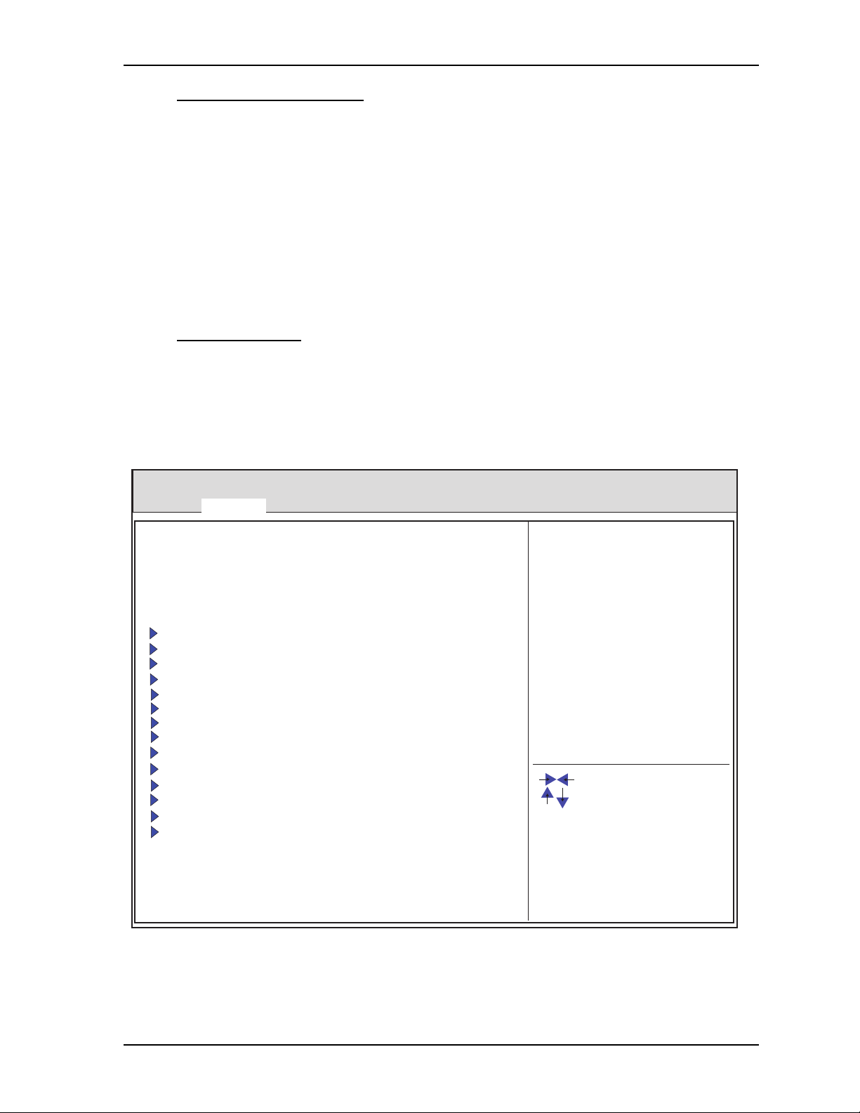
Compact Form Factor
Mini Form Factor
Figure 2-1. Mini, Compact, Basic and Extended Form Factors
Basic Form Factor
Extended Form Factor
Note:
Measurements are in millimeters
COM_FormFactors_b
4 Reference Manual Express-HRR
Page 9

Chapter 2 Product Overview
Product Description
The Express-HRR is an exceptionally high integration, high performance, rugged Intel Core™ i7 processor
based system compatible with the COM Express standard. This rugged and high quality module system
contains all the component subsystems of an ATX motherboard.
The Intel Core i7 incorporates a multi processor core with an integrated Graphics Memory Hub (GMH),
providing a high-performance processor, a memory controller for up to 16GB of SODIMM memory, and a
graphics controller for LVDS, VGA, PCI Express graphics (PEG), SDVO, DisplayPort, and HDMI signals
driven by the PCH.
The Intel BD82QM67 chipset provides controllers for the Platform Controller Hub (PCH) featuring
eight USB 2.0 ports, four SATA ports, eight GPIO ports, and one Gigabit Ethernet interface (external
magnetics required).
Expansion for additional system functions is possible on the Express-HRR through the PCIe and LPC
expansion buses. The PCIe and LPC buses operate at clock speeds of 100MHz and 33MHz, respectively.
The Express-HRR is particularly well suited for either embedded or portable applications and meets the size,
power consumption, temperature range, quality, and reliability demands of embedded system applications.
Module Features
• CPU
♦
Intel 1.5GHz (2610UE), 2.1GHz (2715QE), or 2.2GHz (2655LE), 2nd Generation Core i7 series
processors
♦
DMI (Direct Media Interface) with 2 GB/s of bandwidth in each direction
♦
FDI (Flexible Display Interface) for carrying display traffic to the PCH
♦
Internal 256KB L2 cache
♦
Enhanced Intel SpeedStep® Technology (EIST)
• Memory
♦
Two standard 204-pin DDR3 SODIMM sockets
♦
Supports +1.5V DDR3, 1067/1333MHz RAM up to 16 GB total
♦
Supports ECC, unbuffered memory
• Expansion Buses
♦
PCIe between CPU/PCH and COM Express connectors
♦
LPC (Low Pin Count) for LPC devices
♦
I2C for fast mode I2C devices
• COM Express Interface
♦
SATA Interface
• Provides four SATA ports
• Supports up to 6 Gb/s transfer speed on two ports
• Supports up to 3 Gb/s transfer speed on all ports
• Supports Native Command Queuing
• Provides Auto Activate for DMA
• Supports Hot Plug features
Express-HRR Reference Manual 5
Page 10

Chapter 2 Product Overview
♦
HD Audio
• Provides Intel HD Audio controller
• Supports Audio Docking
• Provides 32-bit sample depth
• Supports sample rates up to 192kHz
♦
USB Port Interface
• Supports two root USB hubs
• Supports eight EHCI USB 2.0 ports
• Supports legacy UHCI USB 1.1 signals
• Supports Per-Port-Disable
♦
Ethernet Interface
• Provides Intel 82579LM Ethernet PHY transceiver chip
• Supports one Gigabit Ethernet port
• Supports IEEE 802.3, 802.3u, 802.3z, and 802.3ab compatible physical layers
• Supports Auto-negotiation for speed, duplex mode, and flow control
• Supports half duplex at 10/100Mb/s or full duplex at 10/100/1000Mb/s
- Full-duplex mode supports transmit and receive frames simultaneously
- Supports IEEE 802.3x flow control in full duplex mode
- Half-duplex mode supports enhanced proprietary collision reduction mode
♦
Video Interfaces (VGA/LVDS/PEG/SDVO/DisplayPort/HDMI)
• Support the DisplayPort standard
• Support Graphics Performance Modulation Technology
• Support Intel Smart 2D Display Technology
• Support Graphics Render C-State
• Support Intel Seamless Display Refresh Rate Switching with eDP
• Provide an integrated RAMDAC with 32-bit color
• Provide digital HSYNC and VSYNC signals
• Support one SDVO port through Digital Port B at 200 MP/s (Megapixels/second)
• Support DisplayPort resolutions up to 2560x1600 at 60 Hz
• Support HDMI (with reduced blanking) resolutions up to 1920x1200 at 60 Hz
• Support VGA resolutions up to 2048x1536 bpp at 75Hz
• Provide 24-bit dual-channel LVDS output
• Support PCI Express Graphics (PEG)
6 Reference Manual Express-HRR
Page 11

Chapter 2 Product Overview
• Miscellaneous
♦
Real Time Clock (RTC) with external replaceable battery
♦
Watchdog Timer (WDT)
♦
TPM (Trusted Platform Module)
♦
Hardware Voltage and Temperature Monitor
♦
Logo Screen (Splash)
Express-HRR Reference Manual 7
Page 12

Chapter 2 Product Overview
Block Diagram
Figure 2-2 shows the functional components of the module.
24-bit, dual channel LVDS
VGA
USB 2.0 (8)
SATA (4)
Intel - HD Audio Link
PCIe X1 (6), Ports 1-6
TPM
VBATT (RTC)
Hardware
Monitor
GPIO
GPIO
Generator
I2C EEPROM
I2C
LVDS DDC I2C
WDT
Board
Controller
PWR Management
Intel Core i7
2610UE 1.5GHz,
2715QE 2.1GHz,
2655LE 2.2GHz
(with integrated Processor Core
and Graphics Memory Hub)
DMI
LPC
SMBus
GPIO
SPI
BD82QM67
CPU
PCH
Intel
FDI
PCIe X1 (1), Port 7
PCIe X1 (1), Port 8
1067/1333MHz,
1.5V, 16GB Max.
Channel - A
Channel - B
PCIe Graphics, 1X16; 2X8;
1X8 & 2X4 - PEG
SDVO / DisplayPort / HDMI
DisplayPort / HDMI
DisplayPort / HDMI
DDR3
SODIMM
Sockets (2)
BIOS
GLAN
COM Express Connector - Rows A and B
SPI
HD Audio
SATA (4)
LVD S
PCIe X1 (6) SMBus
USB 2.0 (8)
LPC
VGA
I2C
GPIO (8)
VBATT WDT
Gigabit
Ethernet
82579LM
Gb Ethernet
12V Input
5V Standby
Intel
COM Express Connector - Rows C and D
SDVO / DP / HDMI DP / HDMI
PCIe X1 (1)
PEG
12V Input
Express-HRR_blkdiag_a
Figure 2-2. Functional Block Diagram
8 Reference Manual Express-HRR
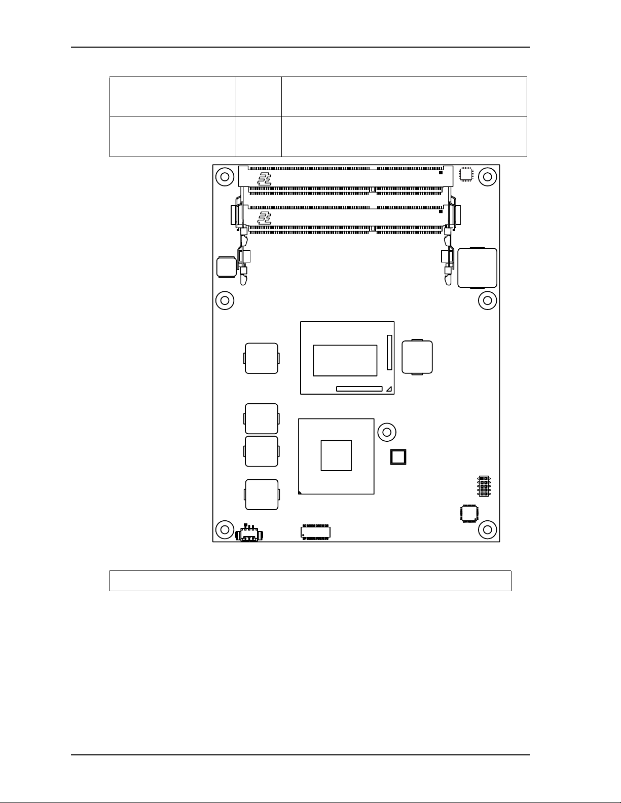
Page 13

Chapter 2 Product Overview
Major Components (ICs)
Table 2-2 lists the major integrated circuits on the Express-HRR, including a brief description of each IC.
Figures 2-3 and 2-4 show the locations of the major ICs.
Table 2-2. Major Integrated Circuit Descriptions and Functions
Chip Type Mfg. Model Description Function
CPU (U1) Intel Core i7 (2610UE,
2715QE, and
2655LE)
PCH (Platform
Controller Hub
[U3])
Hardware
Monitor (U6)
[on bottom side;
see Figure 2-4
on page 11]
TPM (Trusted
Platform
Module [U7])
Board Controller
(U8) [on bottom
side; see
Figure 2-4 on
page 11]
GPIO Generator
(U9)
Gigabit Ethernet
PHY
Transceiver
(U46)
Intel BD82QM67
(PCH)
ON
Semiconductor
Atmel AT97SC3204-
Atmel ATMEGA168V-
Philips PCA9535BS Module providing 16
Intel 82579LM Ethernet PHY
ADT7490-D Remote Voltage and
U1A90
10AU
1.5GHz, 2.1GHz, or
2.2GHz processors with
up to 8MB L3 cache
I/O hub providing
Southbridge functions
(standard I/O functions)
Temperature Monitor
and Fan Controller
Complete turnkey
security solution on a
single chip
Micro controller for
board functions
including I²C,
Watchdog Timer, and
LV DS
bits of GPIO expansion
for I2C/SMBus
applications
transceiver for
10T/100TX/1000T
Gigabit Ethernet
function
Provides
integrated CPU,
memory, and
video
Provides I/O
interfaces such
as USB, SATA,
and video
Provides system
thermal
protection
Provides an
integrated,
protected, nonvolatile solution
for strong public
key security,
intellectual
property
protection,
system integrity,
authentication,
and secure
communications
Optimizes
power
consumption
versus processor
speed
Provides
additional
digital control
lines
Provides a
standard IEEE
802.3 Ethernet
interface for
Ethernet transfer
rate up to 1000
Mb/s
Express-HRR Reference Manual 9
Page 14
Chapter 2 Product Overview
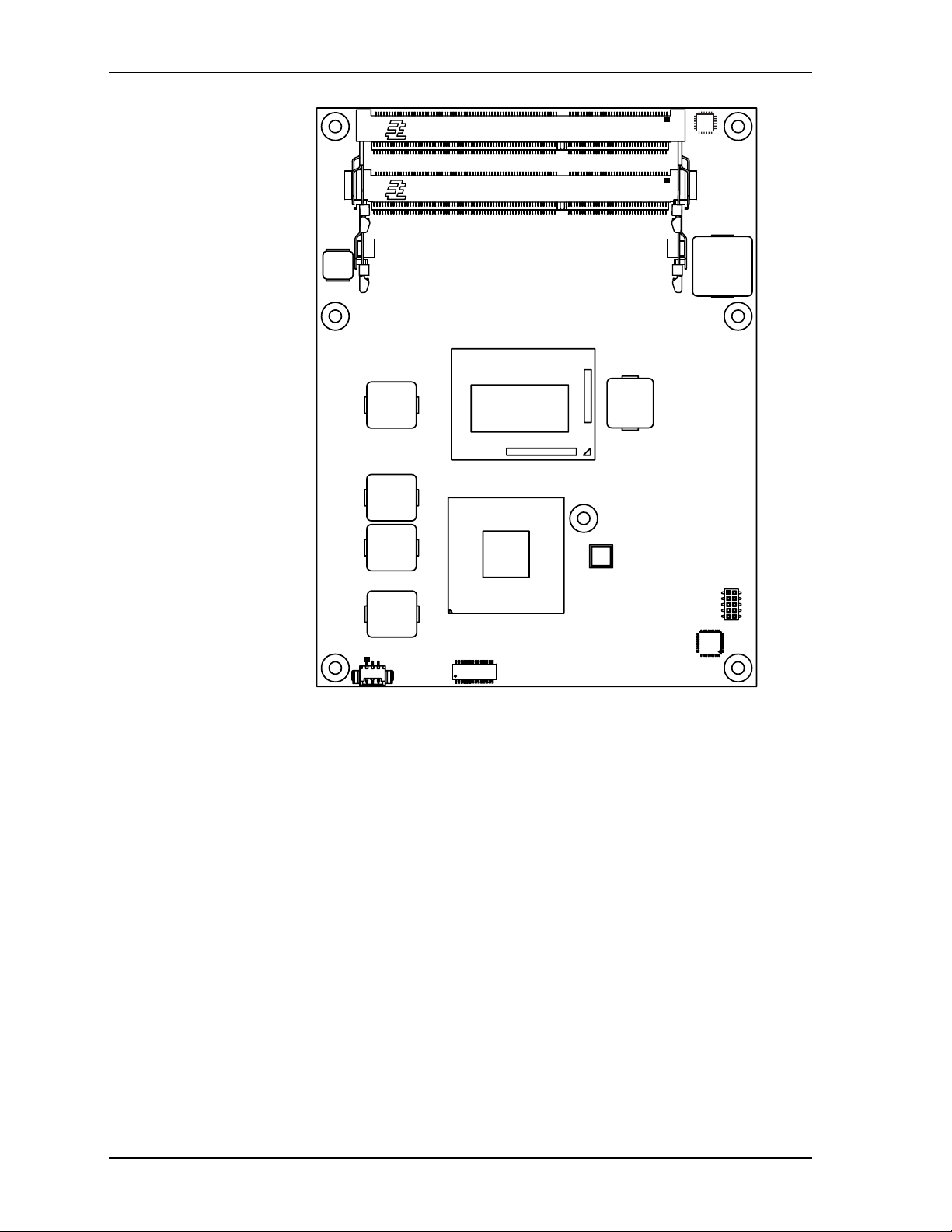
Key:
U1 - CPU
U3 - PCH
U7 - TPM
U9 - GPIO Generator
U46 - Gb Ethernet
U9
U1
U3
U7
Figure 2-3. Component Locations (Top Side)
U46
Express-HRR_Top_Comp_a
10 Reference Manual Express-HRR
Page 15
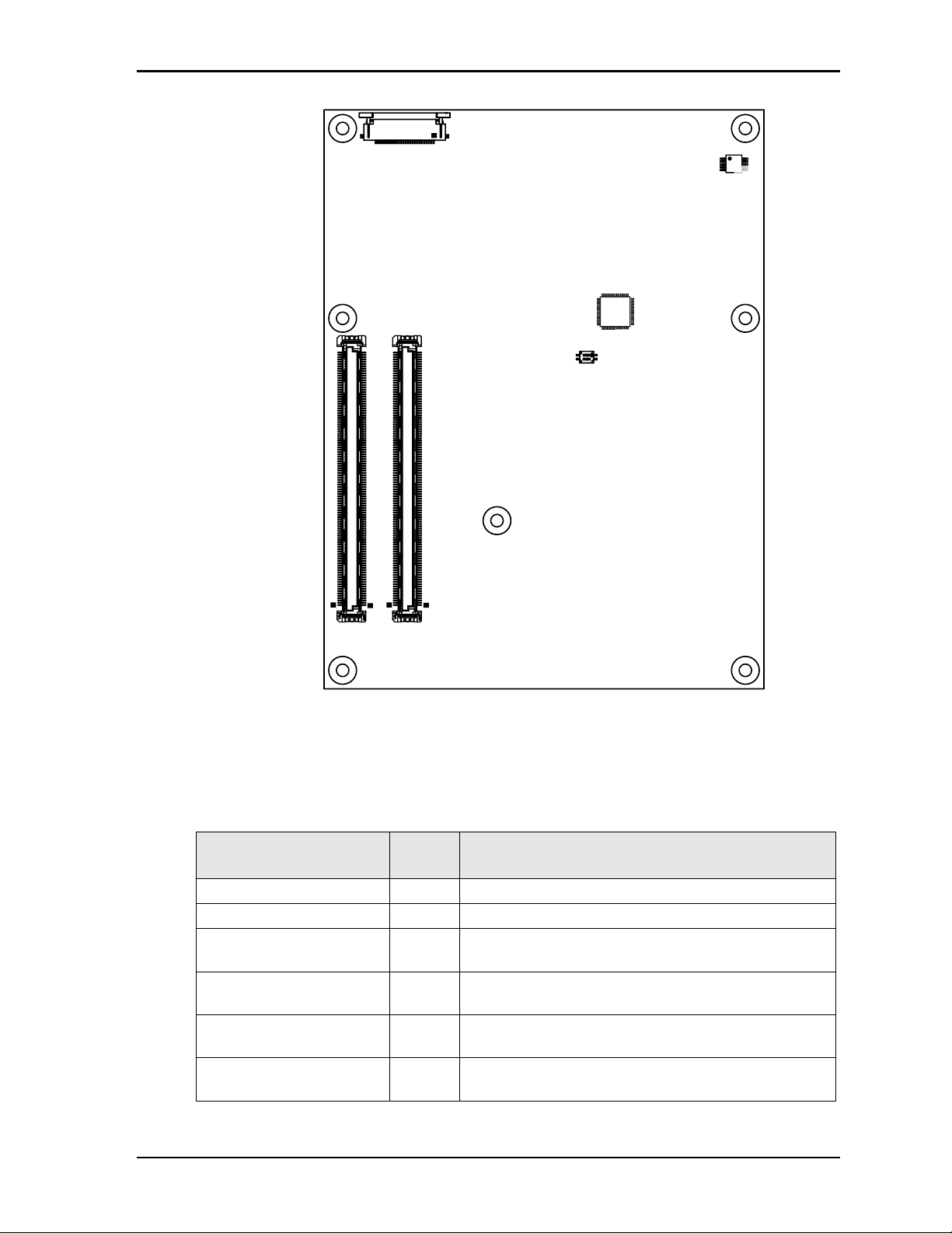
Chapter 2 Product Overview
Key:
U6 - Hardware Monitor
U8 - Board Controller
U6
U8
Figure 2-4. Component Locations (Bottom Side)
Connectors, Headers, and Sockets
Table 2-3 describes the connectors, headers, and sockets shown in Figures 2-5 and 2-6.
Table 2-3. Module Connector and Socket Descriptions
Jack/Plug # Board
Access
J6A – Memory Top 204-pin socket for DDR3 SODIMM - Channel A
J6B – Memory Top 204-pin socket for DDR3 SODIMM - Channel B
CN1 – XDP Debug (see
Bottom 26-pin, 0.020" (0.50mm) right-angle debug port connector
Figure 2-6 on page 13.)
CN4 – LPC Debug Top 10-pin, .050" (1.27mm) female debug port header for
CN6 – COM Express A-B
Bottom 220-pin connector for Northbridge Video and Southbridge
(see Figure 2-6 on page 13.)
CN7 – COM Express C-D
Bottom 220-pin connector for Northbridge Video and Southbridge
(see Figure 2-6 on page 13.)
Description
for the CPU and PCH
issues such as Port 80 POST errors
I/O functions
I/O functions
Express-HRR_Bottom_Comp_a
Express-HRR Reference Manual 11
Page 16
Chapter 2 Product Overview
Table 2-3. Module Connector and Socket Descriptions (Continued)
FAN1 – System Fan Top 3-pin, 0.049" (1.25mm) right-angle shrouded header
controlled by the Hardware Monitor for CPU and PCH
cooling
SW1 – PCIe Bifurcation
Switch (see Figure 2-6 on
Bottom 4-pin dip switch for selecting PCIe modes (positions 1,2 =
1x8, 2x4; 1,3 = reserved; 2,4 = 2x8; 3,4 = 1x16 [Default])
page 13.)
Key:
J6A - Channel A SODIMM socket
J6B - Channel B SODIMM socket
FAN1 - CPU Fan
CN4 - LPC
J6B
J6A
FAN1
CN4
Express-HRR_Top_Conn_a
Figure 2-5. Connector Locations (Top Side)
NOTE Pin 1 is shown as a black square on connectors in all illustrations.
12 Reference Manual Express-HRR
Page 17
Chapter 2 Product Overview
Key:
CN1 - XDP
CN6 - COM Express A1-A110 and B1-B110
CN7 - COM Express C1-C110 and D1-D110
SW1 - PCI Express Bifurcation Switch
CN1
SW1
123
4
CN6
A B
CN7
C D
Figure 2-6. Connector Locations (Bottom Side)
Specifications
Physical Specifications
Table 2-4 lists the physical dimensions of the module.
Table 2-4. Weight and Footprint Dimensions
Item Dimension
Weight 0.09 kg (0.20 lb)
Height (overall) 9.20 mm (0.36 inches)
Board thickness 2.362 mm (0.093 inches)
Width 95.00 mm (3.74 inches)
Length 125.00 mm (4.92 inches)
Express-HRR_Bottom_Conn_a
NOTE Overall height is measured from the
upper board surface to the highest
permanent component on the upper
board surface. This measurement does
not include the cooling solutions. The
heights of the board with the cooling
solutions are 36.50mm for the passive
heatsink (without fan), 46.80mm for the
active heatsink (with fan) and 11.00mm
for the heatspreader.
Express-HRR Reference Manual 13
Page 18
Chapter 2 Product Overview
Power Specifications
Table 2-5 provides the power requirements for the Express-HRR with 1.5, 2.1, and 2.2 GHz CPUs and a 430
watt power supply.
Table 2-5. Power Supply Requirements
Parameter 1.5 GHz CPU 2.1 GHz CPU 2.2 GHz CPU
Input Type
(430 watt power supply)
In-rush Voltage & Current 3.52A (42.24W) 3.76A (45.12W) 7.18A (86.16W)
+12V Regulated DC +12V Regulated DC +12V Regulated DC
Typical Idle Voltage & Current
(Windows XP)
BIT Voltage & Current 1.89A (22.65W) 4.80A (57.59W) 2.72A (32.63W)
S1 Mode 0.13A (0.64W) 0.11A (0.55W) 0.12A (0.60W)
S3 Mode 0.47A (2.37W) 0.46A (2.32W) 0.47A (2.33W)
Operating configurations:
0.66A (7.90W) 0.65A (7.84W) 0.65A (7.78W)
• In-rush operating configuration includes video, baseboard, and 8GB DDR3 RAM.
• Idle (Windows XP) operating configuration includes the in-rush configuration as well as one SATA
drive (external power), boot up from SATA0, keyboard and mouse.
• BIT = Burn-In-Test. Operating configuration includes the Idle configuration as well as a second SATA
hard drive, four USB test plugs, two serial port loop backs, one Ethernet loop back, and two USB
Compact Flash readers with 64MB Compact Flash modules.
• S1 (Standby) operating configuration is the same as BIT operating configuration.
• S3 (Suspend) operating configuration is the same as BIT operating configuration.
Environmental Specifications
Table 2-6 provides the operating and storage temperature ranges required for this module.
Table 2-6. Environmental Requirements
Parameter Conditions
Temperature
Operating –20° to +70°C (–4° to +158°F)
Extended (Optional) –40° to +85°C (–40° to +185°F)
Storage –55° to +85°C (–67° to +185°F)
Humidity
Operating 5% to 90% relative humidity, non-condensing
Non-operating 5% to 95% relative humidity, non-condensing
14 Reference Manual Express-HRR
Page 19

Chapter 2 Product Overview
Thermal/Cooling Requirements
The Express-HRR is designed to operate at its maximum CPU speeds of 1.5GHz, 2.1GHz, and 2.2GHz and
requires a thermal solution to cool the CPU, PCH, and voltage regulators. ADLINK offers two optional
cooling solutions as well as a heat spreader platform on which to build a cooling solution. (See Table 2-7 for
descriptions of cooling options)
NOTE The overall system design must keep the ICs within their operating temperature
specifications.
Table 2-7. ADLINK Optional Cooling Solutions
Cooling Solution Description
Passive Heatsink
(without fan)
Active Heatsink
(with fan)
Heat Spreader Provides a simple thermal platform on which to build a cooling solution.
Qualified to maintain optimal performance up to +70°C.
Qualified to maintain optimal performance up to +85°C. (Note: The
2715QE CPU requires a fan and is qualified only for +70°C.)
1.44
0.22
1.84
0.43
0.22
Heatsink
Fan
1.44
0.22
Heat Spreader
HRR_Cooling_Ht_a
Figure 2-7. Stack Heights of Cooling Assemblies (Side Views)
NOTE All heights are given in inches.
Express-HRR Reference Manual 15
Page 20

Chapter 2 Product Overview
Mechanical Specifications
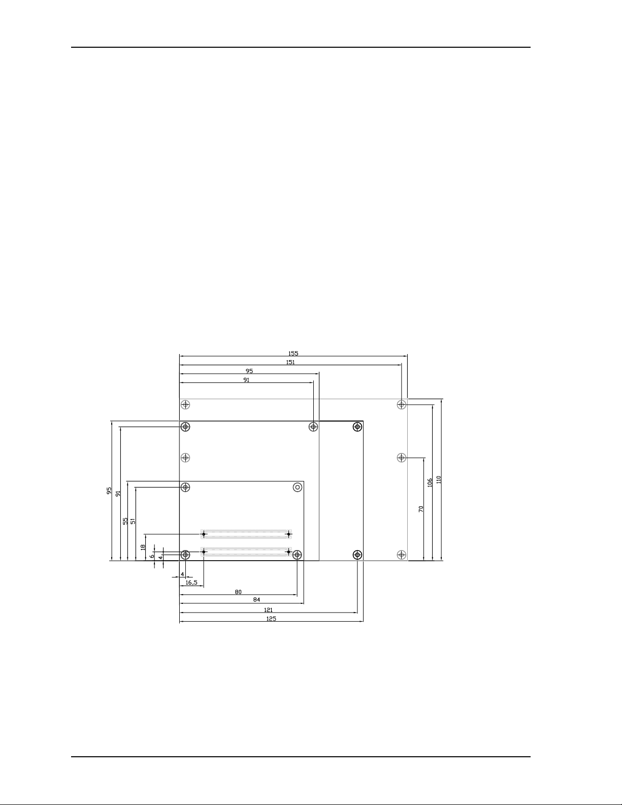
The following figure provides mechanical dimensions of the Express-HRR. Figure 2-8 shows the top-side
view of the board with measurements between mounting holes.
4.92
4.76
4.70
4.15
3.15
2.92
0.16
0.00
Figure 2-8. Mechanical Dimensions (Top Side)
NOTE All dimensions are given in inches.
2.27
3.03
3.50
Express-HRR_mech_dwg_a
1.43
0.65
0.16
0.00
3.74
3.58
16 Reference Manual Express-HRR
Page 21

Chapter 3 Hardware
Overview
This chapter discusses the module features in the following order:
• CPU
• Graphics
• Memory
• Interrupt Channel Assignments
• Memory Map
• I/O Address Map
• COM Express Connector A-B
♦
LPC interface
♦
SATA interface
♦
USB interface
♦
Power interface
♦
Power Management
♦
Video interfaces
♦
HD Audio interface
♦
Gigabit Ethernet interface
♦
I²C interface
♦
PCI Express interface
♦
SMBus
♦
GPIO interface
• COM Express A-B Connector Signals
• COM Express Connector C-D
♦
SDVO / DisplayPort / HDMI interface
♦
DisplayPort / HDMI interface
♦
PCI Express interface
♦
PCI Express Graphics (PEG) interface
• COM Express C-D Connector Signals
• Watchdog Timer
• TPM (Trusted Platform Module)
• Hardware (Voltage and Temperature) Monitor
• System Fan interface signals
Express-HRR Reference Manual 17
Page 22

Chapter 3 Hardware
NOTE ADLINK Technology, Inc. only supports the features/options tested and listed in
this manual. The main chips used in the Express-HRR may provide more
features or options than are listed for the Express-HRR, but some of these
features/options are not supported on the module and will not function as
specified in the chip documentation.
CPU
The Express-HRR offers three versions of the Intel i7 CPU—the 2610UE, 2715QE, and 2655LE—operating
at 1.5GHz, 2.1GHz, and 2.2GHz, respectively. The CPU integrates a high-performance, 64-bit, x86 multi
Processor Core with Memory Controller and 3D Graphics Engine. This single chip is based on 32-nm
process technology and provides an Intel Flexible Display Interface and a Direct Media Interface for highspeed connectivity to the PCH. The CPU also supports Intel Hyper-Threading Technology (4 cores, 8
threads) and up to 16 GB of DDR3 memory at 1066/1333 MHz for high overall performance.
Graphics
The i7 CPU provides a refresh of the sixth generation graphics core, which features a substantial gain in
performance and a decrease in power consumption. The next generation Intel Clear Video HD Technology
includes a collection of video playback and enhancement features that improve the end user’s viewing
experience including Encode/Transcode HD content, HD content playback, and superior image quality.
Other graphics features of the CPU include support for DirectX 10.1, OpenGL3.0, DirectX Video
Acceleration (DXAV), Advanced Scheduler 2.0, 1.0, and XPDM.
Memory
The Express-HRR features dual-stacked SODIMM sockets for up to 16 GB of DDR3 memory. The CPU
provides an Integrated Memory Controller (IMC) with DDR3 protocols and two independent, 64-bit wide
channels each supporting two unbuffered ECC SODIMMs and employing up to two device ranks per
channel.
18 Reference Manual Express-HRR
Page 23
Chapter 3 Hardware
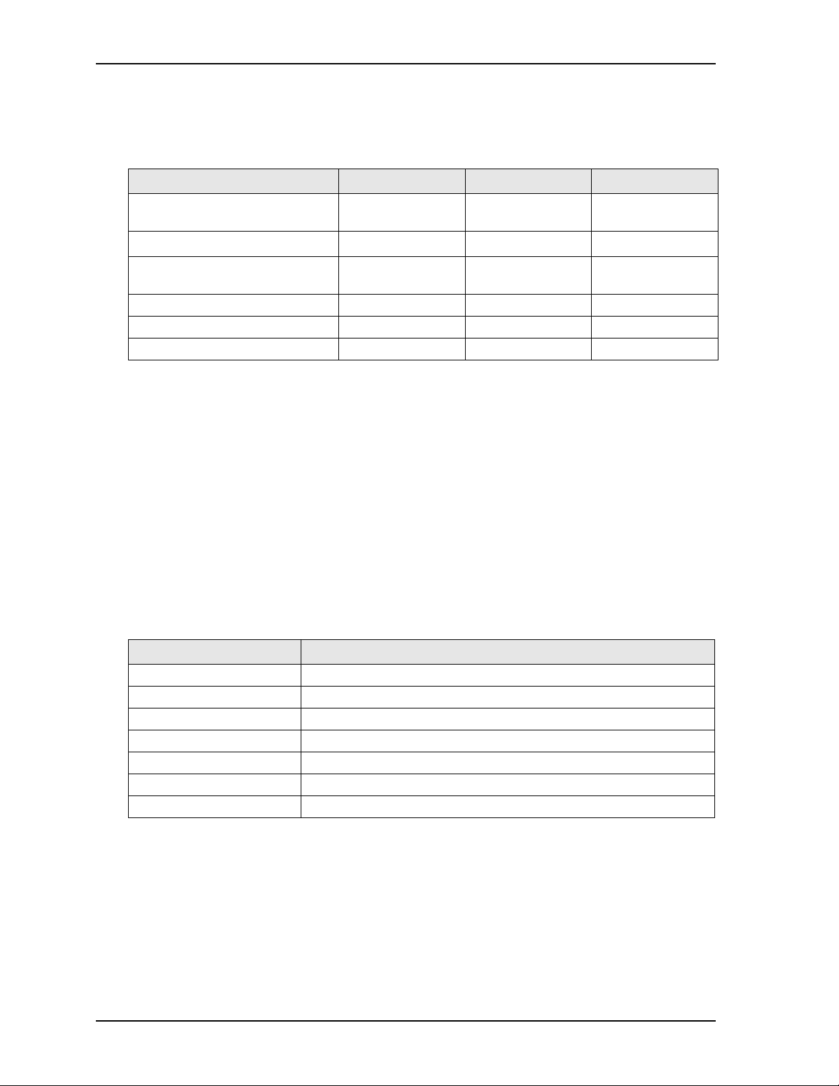
Interrupt Channel Assignments
The interrupt channel assignments are shown in Table 3-1.
NOTE Tab le 3-1 is only for reference. Interrupt channel assignments are tied to the
specific legacy Super I/O device residing on the baseboard. This table can be
used with the baseboard in ADLINK’s Quick Start Kit.
Table 3-1. Interrupt Channel Assignments
Device vs IRQ No. 0 1 2 3 4 5 6 7 8 9 10 11 12 13 14 15
Timer X
PS/2 Keyboard* X
Secondary Cascade X
COM1* O D
COM2* D O
Floppy* D
Parallel* O D
RTC X
Math Coprocessor X
PS/2 Mouse* X
SATA Primary* X
SATA Secondary* X
Audio Controller Automatically Assigned
PCI INTA Automatically Assigned
PCI INTB Automatically Assigned
PCI INTC Automatically Assigned
PCI INTD Automatically Assigned
USB Automatically Assigned
Video Automatically Assigned
Ethernet Automatically Assigned
*Located on the baseboard
Legend: D = Default, X = Fixed, O = Optional
NOTE The IRQs for the Ethernet, Video, and USB are automatically assigned by the
BIOS Plug and Play logic. Local IRQs assigned during initialization can not be
used by external devices.
Express-HRR Reference Manual 19
Page 24

Chapter 3 Hardware
Memory Map
The following table provides the common PC/AT memory allocations. Memory below 000500h is used by
the BIOS.
Table 3-2. Memory Map
Base Address Function
00000000h - 0009FFFFh Conventional Memory
000A0000h - 000AFFFFh Graphics Memory
000B0000h - 000B7FFFh Mono Text Memory
000B8000h - 000BFFFFh Color Text Memory
000C0000h - 000CFFFFh Standard Video BIOS
000D0000h - 000DFFFFh Reserved for Extended BIOS
000E0000h - 000EFFFFh Extended System BIOS Area
000F0000h - 000FFFFFh System BIOS Area (Storage and RAM Shadowing)
Top 32, 64, or 128MB of
Physical Memory
FFE00000h - FFFFFFFFh System Flash
Shared memory of Integrated Graphics enabled
20 Reference Manual Express-HRR
Page 25

Chapter 3 Hardware
I/O Address Map
Table 3-3 shows the I/O address map.
NOTE Tab le 3-3 is only for reference. I/O addresses are tied to the specific legacy
Super I/O device residing on the baseboard. This table can be used with the
baseboard in ADLINK’s Quick Start Kit.
Table 3-3. I/O Address Map
Address (hex) Subsystem
0000-000F Primary DMA Controller
0020-0021 Master Interrupt Controller
0040-0043 Programmable Interrupt Timer (Clock/Timer)
004E-004F TPM (Trusted Platform Module)
0060 Keyboard Controller*
0061 NMI, Speaker control
0063 NMI Controller
0064 Keyboard Controller*
0065 NMI Controller
0067 NMI Controller
0070-007F CMOS RAM, NMI Mask Reg, RT Clock
0080 System reserved
0081-0083 DMA Page Registers
0084-0086 System reserved
0087 DMA Page Register
0088 System reserved
0089-008B DMA Page Registers
008C-008E System reserved
008F DMA Page Register
0090-0091 System reserved
0092 Fast A20 gate and CPU reset*
0093-009F System reserved
00A0-00A1 Slave Interrupt Controller
00A2-00BF System reserved
00C0-00DF Slave DMA Controller #2
00E0-00EF System reserved
00F0-00FF Math Coprocessor
01F0-01F7 SATA Controller
02F8-02FF Serial Port 2 (COM2)*
03B0-03BB Video (monochrome)
03C0-03DF Video (VGA)
03F8-03FF Serial Port 1 (COM1)*
Express-HRR Reference Manual 21
Page 26

Chapter 3 Hardware
Table 3-3. I/O Address Map (Continued)
04D0-04D1 Edge/Level Trigger PIC
0CF9 Reset Control Register
*Located on the baseboard.
COM Express A-B Connector
This section provides descriptions of interfaces within the COM Express A-B connector. The COM Express
connector interface comprises two identical 220-pin connectors (A-B and C-D). The COM Express A-B
connector provides the following features:
• LPC interface
• SATA interface
• USB interface
• Power interface
• Power Management
• Video interfaces
• HD Audio interface
• Gigabit Ethernet interface
• I²C interface
• PCI Express
• SMBus
• GPIO
LPC Interface
The Express-HRR offers the LPC (Low Pin Count) bus through the Intel® BD82QM67 (PCH). Many
devices already exist for this Intel defined bus. The LPC bus corresponds approximately to a serialized ISA
bus yet with a significantly reduced number of signals. Because of the software compatibility to the ISA bus,
I/O extensions such as additional serial ports can be easily implemented on an application specific baseboard
using this bus.
SATA Interface
Four Serial ATA connections are provided through the Intel BD82QM67 (PCH). SATA is an enhancement
of parallel ATA therefore offering higher performance. As a result of this enhancement, the traditional
restrictions of parallel ATA are overcome with respect to speed and EMI. SATA starts with a transfer rate of
1.5 Gb/s and can be expanded up to 3Gb/s on all ports and up to 6 Gb/s on SATA0 and SATA1 in order to
accommodate future developments. SATA is completely protocol and software compatible to parallel ATA.
USB Interface
The PCH offers four UHCI USB host controllers and two EHCI USB host controllers. These controllers
comply with USB standard 1.1 and 2.0 and offer a total of eight USB ports through connector A-B. All ports
are high-speed, full-speed, and low-speed capable. The port routing logic determines whether a USB port is
controlled by one of the UHCI controllers or by one of the EHCI controllers.
Power Interface
A 12V voltage rail on both A-B and C-D COM Express connectors accepts the voltages required for the
board. The RTC 3.3V battery feed and 5V standby functions draw power through the A-B connector.
22 Reference Manual Express-HRR
Page 27

Chapter 3 Hardware
Power Management
The Express-HRR is ACPI 4.0a compliant. The board supports S0, S1, S3, S4, and S5 sleep states.
NOTE Winbond-based baseboards do not support the S3 sleep state on the
Express-HRR.
Video Interfaces
VGA
The Express-HRR graphics are driven by an Intel internal graphics interface which provides the interface for
an analog display. A 340-MHz integrated, 32-bit RAM-based, Digital-to-Analog Converter (RAMDAC)
converts up to 2048x1536 digital pixels at a maximum refresh rate of 75-Hz. Three 8-bit DACs provide R,
G, B signals to the monitor.
LVDS
The Intel BD82QM67 PCH provides direct LVDS output. The output is independent of other panel
interfaces. The LVDS interface will support 1 or 2 channels and can support four data pairs and one clock
pair of LVDS (18 or 24-bit) in each channel.
Audio Interface
The High Definition (HD) Audio controller resides in the PCH and communicates with external codec(s)
(such as audio and modem codecs) over the Intel HD Audio serial link. The PCH implements a single Serial
Data Output signal (AC/HDA_SDOUT) that is connected to all external codecs. Four Serial Digital Input
signals (AC/HDA_SDIN) support up to four codecs.
Ethernet Interface
The Express-HRR supports one Gigabit Ethernet interface, which can be enabled in BIOS Setup. The
Ethernet interface is implemented from the 82579LM Ethernet transceiver and occupies PCI Express port 8.
The Ethernet function supports multi-speed operation 10/100/1000 Mbps and operates in full-duplex at all
supported speeds or half duplex at 10/100 Mbps while adhering to the IEEE 802.3x flow control
specification.
I²C™ Bus
The I²C bus is implemented through the use of the Atmel ATmega168 board controller. The board controller
provides a Fast Mode (400kHz max.) multi-master I²C bus that has maximum I²C bandwidth. Use the
ADLINK Intelligent Device Interface (AIDI) Library for access to the I²C bus. AIDI driver information is
available on the COM Express Product page at: http://www.adlinktech.com
the AIDI User’s Manual describing how to use the I²C bus also reside in the Utilities areas of the COM
Express Product page.
. An AIDI demo program and
Express-HRR Reference Manual 23
Page 28
Chapter 3 Hardware
PCI Express
™
The Express-HRR offers six (6) PCI Express x1 ports (ports 1-6) through the COM Express A-B connector
and two PCI Express x1 ports (ports 7-8) through the C-D connector. These ports can be configured to
support PCI Express edge cards or ExpressCards. Each x1 port supports up to 5 GT/s bandwidth in each
direction. Ports 1-4 and ports 5-8 can be independently configured as four x1s, two x2s, one x2 and two x1s,
or one x4 port widths. The eighth x1 port (port 8) is utilized by the onboard Gigabit Ethernet transceiver and
is unavailable as a PCIe port. The PCI Express interface is based on the PCI Express Specification 2.0.
System Management Bus (SMBus)
The I/O Hub (PCH) contains an integrated SMBus controller with both a host and slave SMBus port; but the
host cannot access the slave internally. The slave port allows an external master access to the PCH through
the COM Express A-B connector. Table 3-4 lists the device names and corresponding reserved addresses on
the SMBus.
Table 3-4. SMBus Reserved Addresses
Component Address (hex)
SODIMM A A0h
SODIMM B A4h
Hardware Temp and Voltage Monitor 2Eh
GPIO Generator 40h
Clock Generator D2h
GPIO
The Express-HRR provides GPIO (General Purpose I/O) pins for custom use through the COM Express AB connector. Use the ADLINK Intelligent Device Interface (AIDI) Library to configure the GPIO interface.
AIDI driver information is available on the COM Express Product page at: http://www.adlinktech.com
AIDI demo program and the AIDI User’s Manual describing how to use the GPIO pins also reside in the
Utilities areas of the COM Express Product page.
For more information about GPIO pin operation, refer to the Intel 6 Series Chipset Datasheet for the PCH
(BD82QM67) controller. Refer to “References” on page 1 for a hyper link to the datasheet.
Table 3-5 provides the pin signals for the COM Express A-B connector.
Table 3-5. COM Express A-B Connector Signal Descriptions
Pin # Row A Pin # Row B
A1 GND B1 GND
A2 GBE0_MDI3- B2 GBE0_ACT# (PU 10k 3.3V)
A3 GBE0_MDI3+ B3 LPC_FRAME#
A4 GBE0_LINK100# (Ethernet Speed LED) B4 LPC_AD0
A5 GBE0_LINK1000# (Ethernet Speed LED) B5 LPC_AD1
A6 GBE0_MDI2- B6 LPC_AD2
A7 GBE0_MDI2+ B7 LPC_AD3
A8 GBE0_LINK# B8 LPC_DRQ0# (Int. PU 20k in PCH)
A9 GBE0_MDI1- B9 LPC_DRQ1# (Int. PU 20k in PCH)
A10 GBE0_MDI1+ B10 LPC_CLK
A11 GND B11 GND
A12 GBE0_MDI0- B12 PWRBTN# (PU 10k 3.3V S5
Standby)
. An
24 Reference Manual Express-HRR
Page 29

Chapter 3 Hardware
Table 3-5. COM Express A-B Connector Signal Descriptions (Continued)
A13 GBE0_MDI0+ B13 SMB_CK (PU 2.2k 3.3V S5 Standby)
A14 GBE0_CTREF B14 SMB_DAT (PU 2.2k 3.3V S5
Standby)
A15 SUS_S3# B15 SMB_ALERT# (PU 10k 3.3V S5 Standby)
A16 SATA0_TX+ B16 SATA1_TX+
A17 SATA0_TX- B17 SATA1_TX-
A18 SUS_S4# B18 SUS_STAT#
A19 SATA0_RX+ B19 SATA1_RX+
A20 SATA0_RX- B20 SATA1_RX-
A21 GND B21 GND
A22 SATA2_TX+ B22 SATA3_TX+
A23 SATA2_TX- B23 SATA3_TX-
A24 SUS_S5# (PU 10k 3.3V S5 Standby) B24 PWR_OK
A25 SATA2_RX+ B25 SATA3_RX+
A26 SATA2_RX- B26 SATA3_RX-
A27 BATLOW# (PU 8.2k 3.3V S5 Standby) B27 WDT
A28 ATA_ACT# (PU 10k 3.3V) B28 AC_SDIN2 (Int. PD 20k in PCH)
A29 AC/HDA_SYNC (Int. PD 20k in PCH) B29 AC_SDIN1 (Int. PD 20k in PCH)
A30 AC/HDA_RST# (Int. PD 20k in PCH) B30 AC_SDIN0 (Int. PD 20k in PCH)
A31 GND B31 GND
A32 AC/HDA_BITCLK (Int. PD 20k in PCH) B32 SPKR (Int. PD 20k in PCH)
A33 AC/HDA_SDOUT (Int. PD 20k in PCH) B33 I2C_CK (PU 4.7k 3.3V)
A34 BIOS_DISABLE# (PU 10k 5V S5
B34 I2C_DAT (PU 4.7k 3.3V)
Standby)
A35 THRMTRIP# (PU 330E 3.3V) B35 THRM#
A36 USB6- (Int. PD 20k in PCH) B36 USB7- (Int. PD 20k in PCH)
A37 USB6+ (Int. PD 20k in PCH) B37 USB7+ (Int. PD 20k in PCH)
A38 USB_6_7_OC# (PU 10k 3.3V S5 Standby) B38 USB_4_5_OC# (PU 10k 3.3V S5 Standby)
A39 USB4- (Int. PD 20k in PCH) B39 USB5- (Int. PD 20k in PCH)
A40 USB4+ (Int. PD 20k in PCH) B40 USB5+ (Int. PD 20k in PCH)
A41 GND B41 GND
A42 USB2- (Int. PD 20k in PCH) B42 USB3- (Int. PD 20k in PCH)
A43 USB2+ (Int. PD 20k in PCH) B43 USB3+ (Int. PD 20k in PCH)
A44 USB_2_3_OC# (PU 10k 3.3V S5 Standby) B44 USB_0_1_OC# (PU 10k 3.3V S5 Standby)
A45 USB0- (Int. PD 20k in PCH) B45 USB1- (Int. PD 20k in PCH)
A46 USB0+ (Int. PD 20k in PCH) B46 USB1+ (Int. PD 20k in PCH)
A47 VCC_RTC B47 EXCD1_PERST# (PU 10k 3.3V S5 Standby)
A48 EXCD0_PERST# (PU 10k 3.3V S5
B48 EXCD1_CPPE# (PU 10k 3.3V)
Standby)
A49 EXCD0_CPPE# (PU 10k 3.3V) B49 SYS_RESET# (PU 10k 5V S5 Standby)
A50 LPC_SERIRQ (PU 10k 3.3V) B50 CB_RESET# (PU 10k 3.3V S5 Standby)
Express-HRR Reference Manual 25
Page 30

Chapter 3 Hardware
Table 3-5. COM Express A-B Connector Signal Descriptions (Continued)
A51 GND B51 GND
A52 PCIE6_TX+ B52 PCIE6_RX+
A53 PCIE6_TX- B53 PCIE6_RX-
A54 GPI0 (PU 10k 3.3V S5 Standby) B54 GPO1 (PU 10k 3.3V S5 Standby)
A55 PCIE5_TX+ B55 PCIE5_RX+
A56 PCIE5_TX- B56 PCIE5_RX-
A57 GND B57 GPO2 (PU 10k 3.3V S5 Standby)
A58 PCIE4_TX+ B58 PCIE4_RX+
A59 PCIE4_TX- B59 PCIE4_RX-
A60 GND B60 GND
A61 PCIE3_TX+ B61 PCIE3_RX+
A62 PCIE3_TX- B62 PCIE3_RX-
A63 GPI1 (PU 10k 3.3V S5 Standby) B63 GPO3 (PU 10k 3.3V S5 Standby)
A64 PCIE2_TX+ B64 PCIE2_RX+
A65 PCIE2_TX- B65 PCIE2_RX-
A66 GND B66 WAKE0# (PU 1k 3.3V S5 Standby)
A67 GPI2 (PU 10k 3.3V S5 Standby) B67 WAKE1# (PU 10k 3.3V S5
Standby)
A68 PCIE1_TX+ B68 PCIE1_RX+
A69 PCIE1_TX- B69 PCIE1_RX-
A70 GND B70 GND
A71 LVDS_A0+ B71 LVDS_B0+
A72 LVDS_A0- B72 LVDS_B0-
A73 LVDS_A1+ B73 LVDS_B1+
A74 LVDS_A1- B74 LVDS_B1-
A75 LVDS_A2+ B75 LVDS_B2+
A76 LVDS_A2- B76 LVDS_B2-
A77 LVDS_VDD_EN (PD 100k) B77 LVDS_B3+
A78 LVDS_A3+ B78 LVDS_B3-
A79 LVDS_A3- B79 LVDS_BKLT_EN (PD 100k)
A80 GND B80 GND
A81 LVDS_A_CK+ B81 LVDS_B_CK+
A82 LVDS_A_CK- B82 LVDS_B_CK-
A83 LVDS_I2C_CK (PU 2.2k 3.3V) B83 LVDS_BKLT_CTRL (PD 100k)
A84 LVDS_I2C_DAT (PU 2.2k 3.3V) B84 VCC_5V_SBY
A85 GPI3 (PU 10k 3.3V S5 Standby) B85 VCC_5V_SBY
A86 RSVD B86 VCC_5V_SBY
A87 RSVD B87 VCC_5V_SBY
A88 PCIE_CK_REF+ B88 BIOS_DS1#
A89 PCIE_CK_REF- B89 VGA_RED (PD 150E)
A90 GND B90 GND
26 Reference Manual Express-HRR
Page 31

Chapter 3 Hardware
Table 3-5. COM Express A-B Connector Signal Descriptions (Continued)
A91 SPI_POWER B91 VGA_GRN (PD 150E)
A92 SPI_MISO B92 VGA_BLU (PD 150E)
A93 GPO0 (PU 10k 3.3V S5 Standby) B93 VGA_HSYNC
A94 SPI_CLK B94 VGA_VSYNC
A95 SPI_MOSI B95 VGA_I2C_CK
A96 TPM_PP B96 VGA_I2C_DAT
A97 TYPE10# (Not Connected) B97 SPI_CS#
A98 SER0_TX (Not Connected) B98 RSVD
A99 SER0_RX (Not Connected) B99 RSVD
A100 GND B100 GND
A101 SER1_TX (Not Connected) B101 FAN_PWMOUT
A102 SER1_RX (Not Connected) B102 FAN_TACHIN
A103 LID# (PU 1k 3.3V) B103 SLEEP#
A104 VCC_12V B104 VCC_12V
A105 VCC_12V B105 VCC_12V
A106 VCC_12V B106 VCC_12V
A107 VCC_12V B107 VCC_12V
A108 VCC_12V B108 VCC_12V
A109 VCC_12V B109 VCC_12V
A110 GND B110 GND
COM Express C-D Connector
The COM Express C-D connector is a 220-pin connector providing the following features:
• Digital Display Interface (DDI)
• PCI Express
• PCI Express Graphics (PEG) interface
• SDVO functionality
Digital Display Interface (DDI)
The Digital Display Interface resides in the PCH and is divided into three digital ports (B, C, D). Each of
these digital ports can be configured natively to drive HDMI and DisplayPort signals. Digital Port B can also
be configured to drive SDVO signals.
PCI Express
The Express-HRR offers six (6) PCI Express x1 ports (ports 1-6) through the COM Express A-B connector
and two PCI Express x1 ports (ports 7-8) through the C-D connector. These ports can be configured to
support PCI Express edge cards or ExpressCards. Each x1 port supports up to 5 GT/s bandwidth in each
direction. Ports 1-4 and ports 5-8 can be independently configured as four x1s, two x2s, one x2 and two x1s,
or one x4 port widths. The eighth x1 port (port 8) is utilized by the onboard Gigabit Ethernet transceiver and
is unavailable as a PCIe port. The PCI Express interface is based on the PCI Express Specification 2.0. The
C-D connector also provides one PCIe x16 port for graphics (PEG) or other PCIe expansion cards and can
be configured using the bifurcation switch (SW1).
™
Express-HRR Reference Manual 27
Page 32

Chapter 3 Hardware
PCI Express Graphics (PEG)
The Express-HRR supports the implementation of a x16 link for an external high-performance PCI Express
Graphics card. It supports a theoretical bandwidth of up to 5GT/s. Each lane of the PEG Port consists of a
receive and transmit differential signal pair designated from PEG_RX8 (+ and -) to PEG_RX15 (+ and -)
and correspondingly from PEG_TX8 (+ and -) to PEG_TX15 (+ and -).
SDVO
The PCH provides Serial Digital Video Output (SDVO) functionality and may be alternatively used for one
third party SDVO compliant device connected to Digital Port B.
Table 3-6 provides the pin signals for the COM Express C-D connector.
Table 3-6. COM Express C-D Connector Signal Descriptions
Pin # Row C Pin # Row D
C1 GND D1 GND
C2 GND D2 GND
C3 USB_SSRX0- (Reserved) D3 USB_SSTX0- (Reserved)
C4 USB_SSRX0+ (Reserved) D4 USB_SSTX0+ (Reserved)
C5 GND D5 GND
C6 USB_SSRX1- (Reserved) D6 USB_SSTX1- (Reserved)
C7 USB_SSRX1+ (Reserved) D7 USB_SSTX1+ (Reserved)
C8 GND D8 GND
C9 USB_SSRX2- (Reserved) D9 USB_SSTX2- (Reserved)
C10 USB_SSRX2+ (Reserved) D10 USB_SSTX2+ (Reserved)
C11 GND D11 GND
C12 USB_SSRX3- (Reserved) D12 USB_SSTX3- (Reserved)
C13 USB_SSRX3+ (Reserved) D13 USB_SSTX3+ (Reserved)
C14 GND D14 GND
C15 DDI1_PAIR6+ D15 DDI1_CTRLCLK_AUX+
(DisplayPanel 1 Aux+ / HDMI1 / SDVO)
C16 DDI1_PAIR6- D16 DDI1_CTRLDATA_AUX-
(DisplayPane11 Aux- / HDMI1 / SDVO)
C17 RSVD D17 RSVD
C18 RSVD D18 RSVD
C19 PCIE_RX7+ D19 PCIE_TX7+
C20 PCIE_RX7- D20 PCIE_TX7-
C21 GND D21 GND
C22 PCIE_RX8+ (Not Available) D22 PCIE_TX8+ (Not Available)
C23 PCIE_RX8- (Not Available) D23 PCIE_TX8- (Not Available)
C24 DDI1_HPD (Hot Plug Detect) D24 RSVD
C25 DDI1_PAIR4+ D25 RSVD
C26 DDI1_PAIR4- D26 DDI1_PAIR0+
C27 RSVD D27 DDI1_PAIR0-
C28 RSVD D28 RSVD
C29 DDI1_PAIR5+ D29 DDI1_PAIR1+
28 Reference Manual Express-HRR
Page 33

Chapter 3 Hardware
Table 3-6. COM Express C-D Connector Signal Descriptions (Continued)
C30 DDI1_PAIR5- D30 DDI1_PAIR1-
C31 GND D31 GND
C32 DDI2_CTRLCLK_AUX+
D32 DDI1_PAIR2+
(DisplayPanel2 Aux+ / HDMI2)
C33 DDI2_CTRLDATA_AUX-
D33 DDI1_PAIR2-
(DisplayPanel2 Aux- / HDMI2)
C34 DDI2_DDC_AUX_SEL
(DisplayPanel2 and HDMI2 Select
D34 DDI1_DDC_AUX_SEL (DisplayPanel 1 and
HDMI1 Select modes; PD 1M GND)
modes; PD 1M GND)
C35 RSVD D35 RSVD
C36 DDI3_CTRLCLK_AUX+
D36 DDI1_PAIR3+ (PU 8.2k 3.3V)
(DisplayPanel3 Aux+ / HDMI3)
C37 DDI3_CTRLDATA_AUX-
D37 DDI1_PAIR3-
(DisplayPanel3 Aux- / HDMI3)
C38 DDI3_DDC_AUX_SEL
D38 RSVD
(DisplayPanel3 and HDMI3 Select
modes; PD 1M GND)
C39 DDI3_PAIR0+ D39 DDI2_PAIR0+
C40 DDI3_PAIR0- D40 DDI2_PAIR0-
C41 GND D41 GND
C42 DDI3_PAIR1+ D42 DDI2_PAIR1+
C43 DDI3_PAIR1- D43 DDI2_PAIR1-
C44 DDI3_HPD (Hot Plug Detect) D44 DDI2_HPD (Hot Plug Detect)
C45 RSVD D45 RSVD
C46 DDI3_PAIR2+ D46 DDI2_PAIR2+ (PU 8.2k 3.3V)
C47 DDI3_PAIR2- D47 DDI2_PAIR2- (PU 8.2k 3.3V)
C48 RSVD D48 RSVD
C49 DDI3_PAIR3+ D49 DDI2_PAIR3+
C50 DDI3_PAIR3- D50 DDI2_PAIR3-
C51 GND D51 GND
C52 PEG_RX0+ D52 PEG_TX0+
C53 PEG_RX0- D53 PEG_TX0-
C54 TYPE0# (Not Connected) D54 PEG_LANE_RV# (Lane reversal)
C55 PEG_RX1+ D55 PEG_TX1+
C56 PEG_RX1- D56 PEG_TX1-
C57 TYPE1# (Not Connected) D57 TYPE2# (PD 0E GND)
C58 PEG_RX2+ D58 PEG_TX2+
C59 PEG_RX2- D59 PEG_TX2-
C60 GND D60 GND
C61 PEG_RX3+ D61 PEG_TX3+
C62 PEG_RX3- D62 PEG_TX3-
C63 RSVD D63 RSVD
Express-HRR Reference Manual 29
Page 34

Chapter 3 Hardware
Table 3-6. COM Express C-D Connector Signal Descriptions (Continued)
C64 RSVD D64 RSVD
C65 PEG_RX4+ D65 PEG_TX4+
C66 PEG_RX4- D66 PEG_TX4-
C67 RSVD D67 GND
C68 PEG_RX5+ D68 PEG_TX5+
C69 PEG_RX5- D69 PEG_TX5-
C70 GND D70 GND
C71 PEG_RX6+ D71 PEG_TX6+
C72 PEG_RX6- D72 PEG_TX6-
C73 RSVD D73 GND
C74 PEG_RX7+ D74 PEG_TX7+
C75 PEG_RX7- D75 PEG_TX7-
C76 GND D76 GND
C77 RSVD D77 RSVD
C78 PEG_RX8+ D78 PEG_TX8+
C79 PEG_RX8- D79 PEG_TX8-
C80 GND D80 GND
C81 PEG_RX9+ D81 PEG_TX9+
C82 PEG_RX9- D82 PEG_TX9-
C83 RSVD D83 RSVD
C84 GND D84 GND
C85 PEG_RX10+ D85 PEG_TX10+
C86 PEG_RX10- D86 PEG_TX10-
C87 GND D87 GND
C88 PEG_RX11+ D88 PEG_TX11+
C89 PEG_RX11- D89 PEG_TX11-
C90 GND D90 GND
C91 PEG_RX12+ D91 PEG_TX12+
C92 PEG_RX12- D92 PEG_TX12-
C93 GND D93 GND
C94 PEG_RX13+ D94 PEG_TX13+
C95 PEG_RX13- D95 PEG_TX13-
C96 GND D96 GND
C97 RSVD D97 RSVD
C98 PEG_RX14+ D98 PEG_TX14+
C99 PEG_RX14- D99 PEG_TX14-
C100 GND D100 GND
C101 PEG_RX15+ D101 PEG_TX15+
C102 PEG_RX15- D102 PEG_TX15-
C103 GND D103 GND
30 Reference Manual Express-HRR
Page 35

Chapter 3 Hardware
Table 3-6. COM Express C-D Connector Signal Descriptions (Continued)
C104 VCC_12V D104 VCC_12V
C105 VCC_12V D105 VCC_12V
C106 VCC_12V D106 VCC_12V
C107 VCC_12V D107 VCC_12V
C108 VCC_12V D108 VCC_12V
C109 VCC_12V D109 VCC_12V
C110 GND D110 GND
Watchdog Timer
The Watchdog Timer (WDT) restarts the system if a mishap occurs, ensuring proper start-up after the
interruption. Possible problems include failure to boot properly, the application software’s loss of control,
failure of an interface device, unexpected conditions on the bus, or other hardware or software malfunctions.
Use the ADLINK Intelligent Device Interface (AIDI) Library to configure the WDT interface. AIDI driver
information is available on the COM Express Product page at: http://www.adlinktech.com
program and the AIDI User’s Manual showing how to use the WDT function also reside in the Utilities areas
of the COM Express Product page.
The WDT (Watchdog Timer) can be used both during the boot process and during normal system operation.
. An AIDI demo
• During the Boot process – If the OS fails to boot in the time interval set in the BIOS, the system will
reset.
Enable the WDT in the Custom Configuration Screen of BIOS Setup. Set the WDT for a time-out
interval in seconds, between 1 and 255, in one second increments. Ensure you allow enough time for the
boot process to complete and for the OS to boot. The OS or application must tickle the WDT as soon as
it comes up. This can be done by accessing the hardware directly or through a BIOS call.
• During System Operation – The user can set up the WDT hardware through a BIOS call or by accessing
the hardware directly using the AIDI Library. The BIOS call must tickle the WDT in the time set when
the WDT is initialized or the system will be reset.
• Watchdog Code example – ADLINK provides a source code example (AIDI demo program) on the
Express-HRR Product page of the web site illustrating how to control the WDT. The code example can
be easily copied to your development environment to compile and test or make any desired changes
before compiling.
TPM (Trusted Platform Module)
The Express-HRR provides a hardware chip called a Trusted Platform Module which is dedicated for
security functions. Trusted Computing is an industry standard created for personal computer security. The
BIOS allows you to enable or disable the TPM.
Hardware Voltage and Temperature Monitor
The Express-HRR provides a hardware monitor to ensure the health of your embedded system with built-in
support for monitoring and control of system temperatures, fan speeds, and critical module voltage levels.
The AIDI Library provides simple APIs at the application level to support these functions and adds alarm
functions when voltage or temperature levels exceed the upper or lower limits set by the user. AIDI driver
information for the Express-HRR is available on the COM Express Product page at:
http://www.adlinktech.com
Hardware Monitor also reside in the Utilities areas of the COM Express Product page.
. An AIDI demo program and the AIDI User’s Manual showing how to use the
Express-HRR Reference Manual 31
Page 36

Chapter 3 Hardware
System Fan
Table 3-7 lists the pin signals of the System Fan interface, which provides a 3-pin, single-row header with
0.049" (1.25mm) pitch.
Table 3-7. Optional System Fan (FAN1)
Pin # Signal Description
1 HWM_PWM2 Modulation – This signal controls the fan speed
2
3
Note: The shaded table cell denotes power or ground.
VCC +5.0/12.0 volts DC +/- 5%
HWM_TACH2 Fan Tachometer – This signal monitors the fan speed
32 Reference Manual Express-HRR
Page 37

Chapter 4 BIOS Setup
Introduction
This section assumes the user is familiar with general BIOS Setup and does not attempt to describe the BIOS
functions. Refer to BIOS Setup Menus in this chapter for a map of the BIOS Setup settings. If ADLINK has
added to or modified any of the standard BIOS functions, these functions will be described.
Entering BIOS Setup (VGA Display)
To enter BIOS Setup using a VGA display for the Express-HRR:
1. Turn on the VGA monitor and the power supply to the Express-HRR.
2. Start Setup by pressing the [Del] key, when the following message appears on the boot screen.
Hit <Del> if you want to run SETUP
3. Use the <Enter> key to select the screen menus listed in the Opening BIOS screen.
4. Follow the instructions at the bottom of each screen to navigate through the selections and modify any
settings.
OEM Logo Screen (Splash Screen)
The Express-HRR BIOS supports a graphical logo screen, which can be customized by the user and
displayed when enabled through the BIOS Setup Utility. The graphical image can be a company logo or any
custom image the user wants to display during the POST process.
NOTE The Quiet Boot feature must be set to Enabled in the Boot settings of BIOS Setup for
the system to recognize the OEM Logo Screen.
Logo Image Requirements
Please contact your ADLINK Sales Representative for more information on OEM Logo Screen
requirements.
Express-HRR Reference Manual 33
Page 38

Chapter 4 BIOS Setup
BIOS Setup Menus
This section provides illustrations of the six main setup screens in the Express-HRR BIOS Setup Utility.
Below each illustration is a bullet list of the screen’s submenus and setting selections. The setting selections
are presented in brackets after each submenu or menu item, and the optimal default settings are presented in
bold. For more detailed definitions of the BIOS settings, refer to the AMI Aptio TSE User Manual:
http://www.ami.com/support/doc/AMI_TSE_User_Manual_PUB.pdf
Table 4-1. BIOS Setup Menus
BIOS Setup Utility Menu Item/Topic
Main BIOS, Memory, and Board information, System Date and Time
Advanced Launch PXE OpROM, Launch Storage OpROM, ACPI, Trusted
Computing, RTC Wake, CPU, USB, SATA, Super IO, Hardware
Monitor, Remote Access, and Sandybridge PPM settings
Chipset System Agent and PCH I/O settings
Boot Boot Up, GateA20, Option ROM Messages, Interrupt 19 Capture, Boot
Order, and Hard Drive BBS Priorities settings
Security Setting or Changing Passwords
Save & Exit Exiting, Saving, Resetting, Save Options, Boot Override settings
BIOS Main Setup Screen
.
Express-HRR REV: XXX
Main Advanced Chipset Boot Security Save & Exit
BIOS Information
BIOS Vendor American Megatrends
Core Version X.X.X.X
Compliency UEFI X.X
Project Version Express-HRR REV: XXX
Build Date and Time XX/XX/XXXX XX:XX:XX
System and Board Information
System Language [Xxxxxxx]
System Date [Xxx XX/XX/20XX]
System Time [XX:XX:XX]
Access Level Administrator
[Setting Description]
: Select Item
Enter : Select
+/- : Change field
F1 : General Help
F2 : Previous Values
F3&F9 : Optimized Defaults
F4 : Save & Exit
F10 : Save & Reset
ESC: Exit
: Select Screen
Express-HRR_BIOS_Main_a
Version X.XX.XXXX. Copyright (C) 20XX American Megatrends, Inc.
Figure 4-1. BIOS Main Setup Screen
34 Reference Manual Express-HRR
Page 39
Chapter 4 BIOS Setup
• System and Board Information
♦
BIOS Rev. [XXX]
♦
BC Firmware Rev. [X.X.X]
♦
Manufacture Date [XX/XX/20XX]
♦
Last Repair Date [XX/XX/20XX]
♦
Serial Number [XXXXXXXXXX]
♦
Hardware Rev [XXXXX-XXXX-XXXX]
♦
LAN MAC ID [XX-XX-XX-XX-XX-XX]
♦
Boot Counter [XXXXXXXX]
♦
Running Time [XXXXX HRs]
• System Date & Time
♦
System Date (day of week, mm:dd:yyyy) – This field requires the alpha-numeric entry of the day of
week, day of the month, calendar month, and all 4 digits of the year, indicating the century plus
year (Fri XX/XX/20XX).
♦
System Time (hh:mm:ss) – This is a 24-hour clock setting in hours, minutes, and seconds.
BIOS Advanced Setup Screen
Express-HRR REV : XXX
Main Advanced Chipset Boot Security Save & Exit
Legacy OpROM Support
Launch PXE OpROM [Disabled]
Launch Storage OpROM [Enabled]
ACPI Settings
Trusted Computing
RTC Wake Settings
CPU Configuration
SATA Configuration
Intel TXT (LT) Configuration
PCH-FW Configuration
Intel Anti-Theft Technology Configuration
AMT Configuration
USB Configuration
ADT 7490 H/W Monitor
Super IO Configuration
Serial Port Console Redirection
Sandybridge PPM Configuration
: Select Item
Enter : Select
+/- : Change field
F1 : General Help
F2 : Previous Values
F3&F9 : Optimized Defaults
F4 : Save & Exit
F10 : Save & Reset
ESC: Exit
[Setting Description]
: Select Screen
Express-HRR_BIOS_Advanced_a
Version X.XX.XXXX. Copyright (C) 20XX American Megatrends, Inc.
Figure 4-2. BIOS Advanced Setup Screen
Express-HRR Reference Manual 35
Page 40

Chapter 4 BIOS Setup
• Legacy OpROM Support
♦
Launch PXE OpROM [Disabled; Enabled]
♦
Launch Storage OpROM [Disabled; Enabled]
• ACPI Settings
♦
ACPI Sleep State [Suspend Disabled; S1 (CPU Stop Clock); S3 (Suspend to RAM)]
♦
Emulation AT/ATX [Emulation AT; ATX]
• Trusted Computing
♦
TPM SUPPORT [Disabled; Enabled]
♦
Current TPM Status Information [depends on board model]
• RTC Wake Settings
♦
RTC Wake Function [Enabled; Disabled]
• CPU Configuration
♦
Intel(R) Core(TM) i7 CPU @ X.XXGHz
♦
Processor ID XXXxX
♦
Microcode Revision 15
♦
Max Processor Speed XXXXMHz
♦
Min Processor Speed XXXMHz
♦
Processor Speed XXXX MHz
♦
Processor Cores X
♦
Intel HT Technology Supported
♦
EMT64 Supported
♦
Hyper-Threading [Disabled; Enabled]
♦
Limit CPUID Maximum [Disabled; Enabled]
♦
Execute Disable Bit [Disabled; Enabled]
♦
Hardware Prefetcher [Disabled; Enabled]
♦
Adjacent Cache Line Prefetch [Disabled; Enabled]
♦
Intel Virtualization [Disabled; Enabled]
• SATA Configuration
♦
SATA Controller(s) [Disabled; Enabled]
♦
SATA Mode Selection [IDE; AHCI; RAID]
♦
Serial ATA Port 0 XXXXXXXXXX (XXX.X)
• Software Preserve Supported
♦
Serial ATA Port 1 Empty
• Software Preserve Unknown
♦
Serial ATA Port 2 Empty
• Software Preserve Unknown
♦
Serial ATA Port 3 Empty
• Software Preserve Unknown
36 Reference Manual Express-HRR
Page 41

Chapter 4 BIOS Setup
• Intel TXT (LT) Configuration
Intel Trusted Execution Technology Configuration
Intel TXT support only can be enabled/disabled if SMX is enabled and must enable the VT support
prior to TXT.
Secure Mode Extensions (SMX) [Disabled]
Intel TXT (LT) Support [Disabled]
• PCH-FW Configuration
♦
ME FW Version X.X.XX.XXXX
♦
ME Firmware Mode Normal Mode
♦
ME Firmware Type Full Sku Firmware
♦
ME Firmware SKU XMB
• Intel Anti-Theft Technology Configuration
♦
Intel Anti-Theft Technology [Disabled; Enabled]
♦
Intel Anti-Theft Technology Recovery [3]
♦
Enter Intel AT Suspend Mode [Disabled; Enabled]
• AMT Configuration
♦
Intel AMT [Disabled; Enabled]
• USB Configuration
♦
USB Devices:
•2 Hubs
♦
Legacy USB Support [Enabled; Disabled]
♦
EHCI Hand-Off [Disabled; Enabled]
♦
USB Hardware delays and Time outs
• USB transfer time-out [1 sec; 5 sec; 10 sec; 20 sec]
• Device Reset Timeout [10 sec; 20 sec; 30 sec; 40 sec]
• Device power-up delay [Auto; Manual]
• ADT 7490 H/W Monitor
♦
Smart Fan Mode Configuration
• Fan1 Smart Fan Mode [Manual Mode; Auto Mode (Module); Auto Mode (ADT 7490); Auto
Mode (CPU)]
• Fan1 expect PWM Output [255]
• Fan2 Smart Fan Mode [Manual Mode; Auto Mode (Module); Auto Mode (ADT 7490); Auto
Mode (CPU)]
• Fan2 expect PWM Output/DC Voltage [255]
♦
Module temperature : +XX C
♦
ADT4790 temperature : +XX C
♦
CPU temperature (By PECI) : +XX C
♦
Module Fan1 Speed (In Module) : N/A
♦
Module Fan2 Speed: (In Carrier) : XXXX RPM
♦
Vtt : +X.XXX V
Express-HRR Reference Manual 37
Page 42

Chapter 4 BIOS Setup
♦
Vccp : +X.XXX V
♦
Vcc : +X.XXX V
♦
+5V : +X.XXX V
♦
+12V : +XX.XXX V
• Super IO Configuration
♦
Serial Port 1 Configuration
• Serial Port [Disabled; Enabled]
• Device Settings IO=3F8h; IRQ=4
♦
Serial Port 2 Configuration
• Serial Port [Disabled; Enabled]
• Device Settings IO=2F8h; IRQ=3
• Serial Port Console Redirection
♦
COM1
• Console Redirection [Disabled; Enabled]
• Console Redirection Settings
- Terminal Type [VT100]
- Bits per second [115200]
- Data Bits [8]
- Stop Bits [1]
- Flow Control [None]
- Recorder Mode [Disabled]
- Resolution 100x31 [Disabled]
- Legacy OS Redirection [80x24]
♦
COM2
• Console Redirection [Disabled; Enabled]
• Console Redirection Settings
- Terminal Type [VT100]
- Bits per second [115200]
- Data Bits [8]
- Stop Bits [1]
- Flow Control [None]
- Recorder Mode [Disabled]
- Resolution 100x31 [Disabled]
- Legacy OS Redirection [80x24]
• Sandybridge PPM Configuration
♦
EIST [Disabled; MAX Speed; MIN Speed]
♦
Turbo Mode [Disabled; Enabled]
♦
CPU C3 Report [Disabled; Enabled]
♦
CPU C6 Report [Disabled; Enabled]
♦
CPU C7 Report [Disabled; Enabled]
38 Reference Manual Express-HRR
Page 43

Chapter 4 BIOS Setup
BIOS Chipset Setup Screen
Express-HRR REV : XXX
Main Advanced Chipset Boot Security Save & Exit
System Agent (SA) Configuration
PCH-IO Configuration
Version X.XX.XXXX. Copyright (C) 20XX American Megatrends, Inc.
[Setting Description]
: Select Screen
: Select Item
Enter : Select
+/- : Change field
F1 : General Help
F2 : Previous Values
F3&F9 : Optimized Defaults
F4 : Save & Exit
F10 : Save & Reset
ESC: Exit
Express-HRR_BIOS_Chipset_a
Figure 4-3. BIOS Chipset Setup Screen
• System Agent (SA) Configuration
♦
System Agent RC Version X.X.X.X
♦
VT-d Capability Supported
♦
VT-d [Disabled; Enabled]
♦
Graphics Configuration
• IGFX VBIOS Version XXXX
• IGFX Frequency XXX MHz
♦
Primary Display [Auto; IGFX; PEG]
♦
Internal Graphics [Disabled; Enabled]
♦
GTT Size [1MB; 2MB]
♦
Aperture Size [128MB; 256MB; 512MB]
♦
DVMT Pre-Allocated [0M; 32M; 64M; 96M; 128M; 160M; 192M; 224M; 256M; 288M; 320M;
352M; 384M; 416M; 448M; 480M; 512M]
♦
DVTM Total Gfx Mem [128M; 256M; MAX]
Express-HRR Reference Manual 39
Page 44

Chapter 4 BIOS Setup
♦
LCD Control
• Primary IGFX Boot Display [Auto; CRT; CRT + LVDS; DDI; DDI2; DDI3; LVDS]
• DDI function choose [DisplayPort; HDMI]
• LCD Panel Type [640x480 LVDS; 800x600 LVDS; 1024x768 LVDS; 1280x1024 LVDS;
1400x1050 LVDS1; 1400x1050 LVDS2; 1600x1200 LVDS; 1366x768 LVDS; 1680x1050
LVDS; 1920x1200 LVDS; 1440x900 LVDS; 1600x900 LVDS; 1280x800 LVDS; 1920x1080
LVDS; 2048x1536 LVDS]
• Active LFP [No LVDS; Int-LVDS]
• Panel Color Depth [18 Bit; 24 Bit]
• GTT LVDS Backlight Controller [0%; 20%; 40%; 60%; 80%; 100%]
• GTT LVDS Backlight Inverter [PWM Inverted; PWM Normal]
♦
NB PCIe Configuration
• PEG0 Not Present
• PEG1 Not Present
• PEG2 Not Present
• PEG3 Not Present
♦
Memory Information
• Memory RC Version X.X.X.X
• Memory Frequency XXXX Mhz
• Total Memory XXXX MB (DDR3)
• DIMM#0 Not Present
• DIMM#1 Not Present
• DIMM#2 XXXX MB (DDR3)
• DIMM#3 Not Present
• CAS Latency (tCL) X
• Minimum delay time
-CAS to RAS (tRCDmin) X
-Row Precharge (tRRmin) X
-Active to Precharge (tRASmin) XX
• PCH-IO Configuration
♦
Intel PCH RC Version X.X.X.X
♦
Intel PCH SKU Name QMXX
♦
Intel PCH Rev ID XX/XX
♦
PCH LAN Controller [Enabled; Disabled]
♦
Azalia [Enabled; Disabled]
♦
Restore AC Power Loss [Power Off; Power On; Last State]
♦
DC I2C Speed Control [100khz; 200khz; 400khz]
♦
Sleep & LID Button [Enabled; Disabled]
40 Reference Manual Express-HRR
Page 45
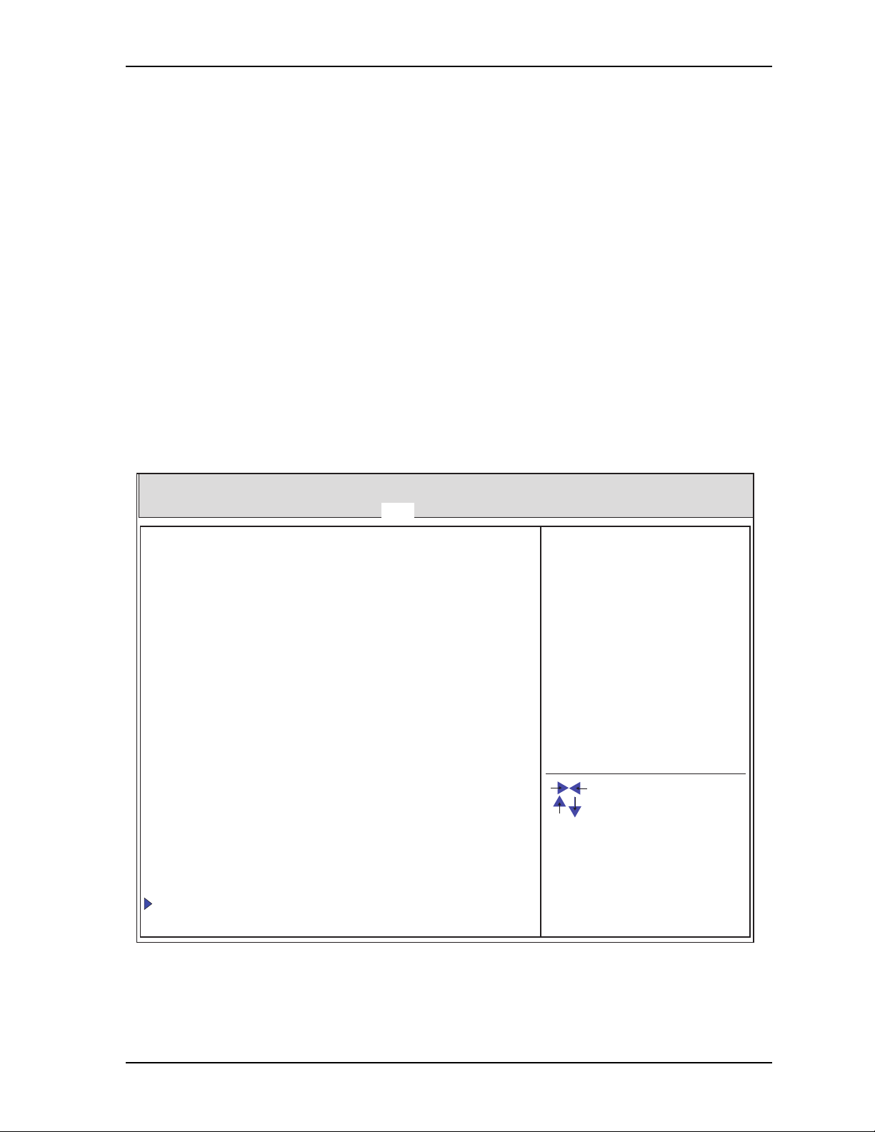
Chapter 4 BIOS Setup
♦
USB Configuration
•EHCI1 [Enabled; Disabled]
•EHCI2 [Enabled; Disabled]
♦
PCI Express Configuration
• Target Link Speed [GEN1; GEN2]
• PCIE Ports 1-4 Configuration [Four X1 Ports; One X4 Port]
• PCI Express Root Port 1 (Main Switch) [Disabled; Enabled]
• PCI Express Root Port 2 [Disabled; Enabled]
• PCI Express Root Port 3 [Disabled; Enabled]
• PCI Express Root Port 4 [Disabled; Enabled]
• PCI Express Root Port 5 [Disabled; Enabled]
• PCI Express Root Port 6 [Disabled; Enabled]
• PCI Express Root Port 7 [Disabled; Enabled]
• PCI Express Port 8 is assigned to LAN
BIOS Boot Setup Screen
Express-HRR REV : XXX
Main Advanced Chipset Boot Security Save & Exit
Boot Configuration
Setup Prompt Timeout 1
Bootup NumLock State [On]
Quiet Boot [Disabled]
CSM16 Module Version XX.XX
GateA20 Active [Upon Request]
Option ROM Messages [Force BIOS]
Interrupt 19 Capture [Enabled]
Set Boot Priorities
1st Boot [CD/DVD]
2nd Boot [Hard Disk : Xxxxxxxx]
3rd Boot [USB Floppy]
4th Boot [USB CD/DVD]
5th Boot [USB Hard Disk]
6th Boot [USB Key]
7th Boot [Network]
8th Boot [UEFI]
Hard Drive BBS Priorities
Enter : Select
+/- : Change field
F1 : General Help
F2 : Previous Values
F3&F9 : Optimized Defaults
F4 : Save & Exit
F10 : Save & Reset
ESC: Exit
[Setting Description]
: Select Screen
: Select Item
Express-HRR_BIOS_Boot_a
Version X.XX.XXXX. Copyright (C) 20XX American Megatrends, Inc.
Figure 4-4. BIOS Boot Setup Screen
Express-HRR Reference Manual 41
Page 46

Chapter 4 BIOS Setup
• Boot Configuration
♦
Setup Prompt Timeout 1
♦
Bootup NumLock State [On; Off]
♦
Quiet Boot [Disabled; Enabled]
• CSM16 Module Version XX.XX
♦
Gate A20 Active [Upon Request; Always]
♦
Option ROM Messages [Force BIOS; Keep Current]
♦
Interrupt 19 Capture [Disabled; Enabled]
• Set Boot Priority
♦
1st Boot [CD/DVD; Hard Disk : Xxxxxxx; USB Floppy; USB CD/DVD; USB Hard Disk; USB
Key; Network; UEFI; Disabled]
♦
2nd Boot [CD/DVD; Hard Disk : Xxxxxxx; USB Floppy; USB CD/DVD; USB Hard Disk; USB
Key; Network; UEFI; Disabled]
♦
3rd Boot [CD/DVD; Hard Disk : Xxxxxxx; USB Floppy; USB CD/DVD; USB Hard Disk; USB
Key; Network; UEFI; Disabled]
♦
4th Boot [CD/DVD; Hard Disk : Xxxxxxx; USB Floppy; USB CD/DVD; USB Hard Disk; USB
Key; Network; UEFI; Disabled]
♦
5th Boot [CD/DVD; Hard Disk : Xxxxxxx; USB Floppy; USB CD/DVD; USB Hard Disk; USB
Key; Network; UEFI; Disabled]
♦
6th Boot [CD/DVD; Hard Disk : Xxxxxxx; USB Floppy; USB CD/DVD; USB Hard Disk; USB
Key; Network; UEFI; Disabled]
♦
7th Boot [CD/DVD; Hard Disk : Xxxxxxx; USB Floppy; USB CD/DVD; USB Hard Disk; USB
Key; Network; UEFI; Disabled]
♦
8th Boot [CD/DVD; Hard Disk : Xxxxxxx; USB Floppy; USB CD/DVD; USB Hard Disk; USB
Key; Network; UEFI; Disabled]
♦
Hard Disk BBS Priorities [SATA: Xxxxxxxx; Disabled]
42 Reference Manual Express-HRR
Page 47

Chapter 4 BIOS Setup
BIOS Security Setup Screen
Express-HRR REV : XXX
Main Advanced Chipset Boot Security Save & Exit
Password Description
If ONLY the Administrator’s password is set,
then this only limits access to Setup and is
only asked for when entering Setup.
If ONLY the User’s password is set, then this
is a power on password and must be entered to
boot or enter Setup. In Setup the User will
have Administrator rights.
The password must be 3 to 20 characters long.
Administrator Password
User Password
HDD Security Configuration
HDD X:XXXXXXXXXXX
[Setting Description]
: Select Screen
: Select Item
Enter : Select
+/- : Change field
F1 : General Help
F2 : Previous Values
F3&F9 : Optimized Defaults
F4 : Save & Exit
F10 : Save & Reset
ESC: Exit
Express-HRR_BIOS_Security_a
Version X.XX.XXXX. Copyright (C) 20XX American Megatrends, Inc.
Figure 4-5. BIOS Security Setup Screen
• Administrator Password [Create New Password]
• User Password [Create New Password]
• HDD Security Configuration
♦
HDD 0: XXXXXXXXXXX
Express-HRR Reference Manual 43
Page 48
Chapter 4 BIOS Setup
BIOS Save & Exit Setup Screen
Express-HRR REV : XXX
Main Advanced Chipset Boot Security Save & Exit
Save Changes and Exit
Discard Changes and Exit
Save Changes and Reset
Discard Changes and Reset
Save Options
Save Changes
Discard Changes
Restore Defaults
Save as User Defaults
Restore User Defaults
Boot Override
SATA: XXXXXXXXXXX
Launch EFI Shell from filesystem device
[Setting Description]
: Select Screen
: Select Item
Enter : Select
+/- : Change field
F1 : General Help
F2 : Previous Values
F3&F9 : Optimized Defaults
F4 : Save & Exit
F10 : Save & Reset
ESC: Exit
Express-HRR_BIOS_Save&Exit_a
Version X.XX.XXXX. Copyright (C) 20XX American Megatrends, Inc.
♦
Save Changes and Exit
• Save configuration and exit? [Ye s ; No]
♦
Discard Changes and Exit
• Quit without saving? [Ye s ; No]
♦
Save Changes and Reset
• Save configuration and reset? [Ye s ; No]
♦
Discard Changes and Reset
• Reset without saving? [Ye s ; No]
• Save Options
♦
Save Changes
• Save configuration [Ye s ; No]
♦
Discard Changes
• Load Previous Values [Ye s ; No]
♦
Restore Defaults
• Load Optimized Defaults [Ye s ; No]
Figure 4-6. BIOS Save & Exit Setup Screen
44 Reference Manual Express-HRR
Page 49

Chapter 4 BIOS Setup
♦
Save as User Defaults
• Save configuration? [Ye s ; No]
♦
Restore User Defaults
• Restore User Defaults? [Ye s ; No]
• Boot Override
♦
SATA: XXXXXXXXXXX
♦
Launch EFI Shell from file system device
Express-HRR Reference Manual 45
Page 50

Chapter 4 BIOS Setup
46 Reference Manual Express-HRR
Page 51

Appendix A Technical Support
Contact us should you require any service or assistance.
ADLINK Technology, Inc.
Address: 9F, No.166 Jian Yi Road, Zhonghe District
New Taipei City 235, Taiwan
ᄅקؑխࡉ৬ԫሁ 166 ᇆ 9 ᑔ
Tel: +886-2-8226-5877
Fax: +886-2-8226-5717
Email: service@adlinktech.com
Ampro ADLINK Technology, Inc.
Address: 5215 Hellyer Avenue, #110, San Jose, CA 95138, USA
Tel: +1-408-360-0200
Toll Free: +1-800-966-5200 (USA only)
Fax: +1-408-360-0222
Email: info@adlinktech.com
ADLINK Technology (China) Co., Ltd.
Address: Ϟ⍋Ꮦ⌺ϰᮄᓴ∳催⾥ᡔು㢇䏃 300 ো(201203)
300 Fang Chun Rd., Zhangjiang Hi-Tech Park,
Pudong New Area, Shanghai, 201203 China
Tel: +86-21-5132-8988
Fax: +86-21-5132-3588
Email: market@adlinktech.com
ADLINK Technology, Inc. provides a number of methods for contacting Technical Support listed in the
Table A-1 below. Requests for support through the Ask an Expert are given the highest priority, and usually
will be addressed within one working day.
• ADLINK Ask an Expert – This is a comprehensive support center designed to meet all your technical
needs. This service is free and available 24 hours a day through the Ampro By ADLINK web page at
http://www.adlinktech.com/AAE/
which will help you with the common information requested by most customers. This is a good source
of information to look at first for your technical solutions. However, you must register online if you
wish to use the Ask a Question feature.
ADLINK strongly suggests that you register with the web site. By creating a profile on the ADLINK
web site, you will have a portal page called “My ADLINK” unique to you with access to exclusive
services and account information.
• Personal Assistance – You may also request personal assistance by creating an Ask an Expert account
and then going to the Ask a Question feature. Requests can be submitted 24 hours a day, 7 days a week.
You will receive immediate confirmation that your request has been entered. Once you have submitted
your request, you must log in to go to the My Question area where you can check status, update your
request, and access other features.
• Download Service – This service is also free and available 24 hours a day at
http://www.adlinktech.com
register online before you can log in to this service.
. This includes a searchable database of Frequently Asked Questions,
. For certain downloads such as technical documents and software, you must
Table A-1. Technical Support Contact Information
Method Contact Information
Ask an Expert http://www.adlinktech.com/AAE/
Web Site http://www.adlinktech.com
Standard Mail
Express-HRR Reference Manual 47
Page 52

Appendix A Technical Support
ADLINK Technology Beijing
Address: ࣫ҀᏖ⍋⎔Ϟഄϰ䏃 1 োⲜ߯ࡼ E ᑻ 801 ᅸ(100085)
Rm. 801, Power Creative E, No. 1, B/D
Shang Di East Rd., Beijing, 100085 China
Tel: +86-10-5885-8666
Fax: +86-10-5885-8625
Email: market@adlinktech.com
ADLINK Technology Shenzhen
Address: ⏅ഇᏖቅ⾥ᡔು催ᮄϗ䘧᭄ᄫᡔᴃು
A1 2 ὐ C (518057)
2F, C Block, Bldg. A1, Cyber-Tech Zone, Gao Xin Ave. Sec. 7,
High-Tech Industrial Park S., Shenzhen, 518054 China
Tel: +86-755-2643-4858
Fax: +86-755-2664-6353
Email: market@adlinktech.com
Table A-1. Technical Support Contact Information (Continued)
ADLINK Technology (Europe) GmbH
Address: Nord Carree 3, 40477 Duesseldorf, Germany
Tel: +49-211-495-5552
Fax: +49-211-495-5557
Email: emea@adlinktech.com
ADLINK Technology, Inc. (French Liaison Office)
Address: 15 rue Emile Baudot, 91300 Massy CEDEX, France
Tel: +33 (0) 1 60 12 35 66
Fax: +33 (0) 1 60 12 35 66
Email: france@adlinktech.com
ADLINK Technology Japan Corporation
Address: ͱ101-0045 ᵅҀ䛑ҷ⬄⼲⬄䤯ފ⬎ 3-7-4
⼲⬄ 374 ɛɳ 4F
KANDA374 Bldg. 4F, 3-7-4 Kanda Kajicho,
Chiyoda-ku, Tokyo 101-0045, Japan
Tel: +81-3-4455-3722
Fax: +81-3-5209-6013
Email: japan@adlinktech.com
ADLINK Technology, Inc. (Korean Liaison Office)
Address: 昢殾柢 昢爎割 昢爎壟 1506-25 穢壊 B/D 2 猻
2F, Hando B/D, 1506-25, Seocho-Dong, Seocho-Gu,
Seoul 137-070, Korea
Tel: +82-2-2057-0565
Fax: +82-2-2057-0563
Email: korea@adlinktech.com
ADLINK Technology Singapore Pte. Ltd.
Address: 84 Genting Lane #07-02A, Cityneon Design Centre,
Singapore 349584
Tel: +65-6844-2261
Fax: +65-6844-2263
Email: singapore@adlinktech.com
ADLINK Technology Singapore Pte. Ltd. (Indian Liaison Office)
Address: No. 1357, "Anupama", Sri Aurobindo Marg, 9th Cross,
JP Nagar Phase I, Bangalore - 560078, India
Tel: +91-80-65605817
Fax: +91-80-22443548
48 Reference Manual Express-HRR
Email: india@adlinktech.com
Page 53

Index
A
Advanced BIOS screen ....................................... 35
AIDI Library user’s manual
AMI BIOS User’s Guide
architecture
audio
........................................................... 4
...............................................................6, 23
.................................. 1
...................................... 2
B
Basic form factor .................................................. 3
BIOS Setup Utility
block diagram
board controller
board dimensions
Boot BIOS screen
........................................33, 34
....................................................... 8
.................................................2, 9
................................................ 13
............................................... 41
C
chip specifications ................................................ 2
COM Express A-B connector
COM Express C-D connector
COM Express concept
Compact form factor
components (ICs)
connectors, headers, and sockets
Cooling Solution
Core i7
................................................... 2, 5, 9, 18
CPU description
current
................................................................. 14
............................................. 3
.................................................. 9
................................................. 15
..........................................5, 9, 18
............................. 22
............................. 27
.......................................... 3
........................ 11
D
DDI ..................................................................... 27
DDR3 SODIMM
dimensions
DisplayPort
.................................................. 5
.......................................................... 13
........................................................... 3
E
Environmental specifications .............................. 14
Ethernet
expansion buses
Extended form factor
...........................................................6, 23
.................................................... 5
............................................ 3
F
fan ....................................................................... 32
features list
form factors
............................................................ 5
........................................................... 3
G
Gigabit Ethernet interface ...............................6, 23
GPIO
...........................................................2, 9, 24
graphics
............................................................... 18
H
hardware overview .............................................. 17
hardware voltage and temperature monitor
HD Audio interface
HDMI
.................................................................... 3
heatsink
height
.........................................................13, 15
.................................................................. 13
.........................................6, 23
....7, 31
I
I/O address map ...................................................21
I2C
.......................................................................23
integrated circuits
Interrupt (IRQs) list
..................................................9
.............................................19
L
length ...................................................................13
Logo Screen (Splash)
LPC Interface
LVDS
......................................................22
.............................................................. 3, 23
............................................7
M
Main BIOS Screen ...............................................34
major integrated circuits
mechanical diagram
memory
memory map
Mini form factor
miscellaneous features
module features
........................................................... 5, 18
........................................................20
....................................................3
.....................................................5
........................................9
.............................................16
...........................................7
O
operating configurations ......................................14
P
PCH .................................................................. 2, 9
PCI Express
PCI Express Graphics (PEG)
PHY transceiver
pin-out types
power interface
power management
product description
.................................................. 24, 27
..............................28
............................................... 2, 9
..........................................................3
....................................................22
..............................................23
................................................5
R
Real Time Clock (RTC) ........................................7
references
...............................................................1
S
SATA interface ............................................... 5, 22
Save & Exit BIOS screen
SDVO
............................................................. 3, 28
Security BIOS screen
site preparation
environmental requirements
SMBus
.................................................................24
SODIMM
specification references
Splash Screen (Logo Screen)
supported features
.............................................................18
Core i7 CPU
CPU fan header
DDR3 SODIMM
expansion buses
Gigabit Ethernet interface
hardware voltage and temperature monitor
HD Audio
.............................................. 5, 18
........................................................6
....................................44
..........................................43
..........................14
.........................................1
..............................33
..............................................32
.............................................5
...............................................5
................................6
.....7
Express-HRR Reference Manual 49
Page 54

Index
IRQ assignments
Logo Screen (Splash)
memory map
Real Time Clock (RTC)
SATA
.............................................................. 5
TPM (Trusted Platform Module)
USB ports
video interfaces
Watchdog Timer
System fan pin-out list
........................................... 19
................................7, 33
.................................................. 20
.................................. 7
.................... 7
........................................................ 6
............................................... 6
........................................7, 31
........................................32
T
Technical references ............................................. 1
Technical Support
Ask an Expert (on-line)
contact information
temperature monitor
thermal cooling
requirements
thickness
TPM (Trusted Platform Module)
.............................................................. 13
.................................................. 15
.................................47
....................................... 47
........................................9, 31
........... 2, 7, 9, 31
U
unsupported features ........................................... 18
USB interface
.................................................6, 22
V
VGA ................................................................3, 23
video interfaces
voltage
................................................................ 14
voltage monitor
...............................................6, 23
...............................................9, 31
W
Watchdog Timer .............................................7, 31
web sites
AMI BIOS 8 user’s guide
weight
................................................................. 13
width
................................................................... 13
............................... 2
50 Reference Manual Express-HRR
 Loading...