

Page 1

INTEGRATED CIRCUITS
ADC0803/0804
CMOS 8-bit A/D converters
Product data
Supersedes data of 2001 Aug 03
2002 Oct 17
Page 2
Philips Semiconductors Product data
ADC0803/0804CMOS 8-bit A/D converters
DESCRIPTION
The ADC0803 family is a series of three CMOS 8-bit successive
approximation A/D converters using a resistive ladder and
capacitive array together with an auto-zero comparator. These
converters are designed to operate with microprocessor-controlled
buses using a minimum of external circuitry. The 3-State output data
lines can be connected directly to the data bus.
The differential analog voltage input allows for increased
common-mode rejection and provides a means to adjust the
zero-scale offset. Additionally, the voltage reference input provides a
means of encoding small analog voltages to the full 8 bits of
resolution.
FEATURES
•Compatible with most microprocessors
•Differential inputs
•3-State outputs
•Logic levels TTL and MOS compatible
•Can be used with internal or external clock
•Analog input range 0 V to V
CC
•Single 5 V supply
•Guaranteed specification with 1 MHz clock
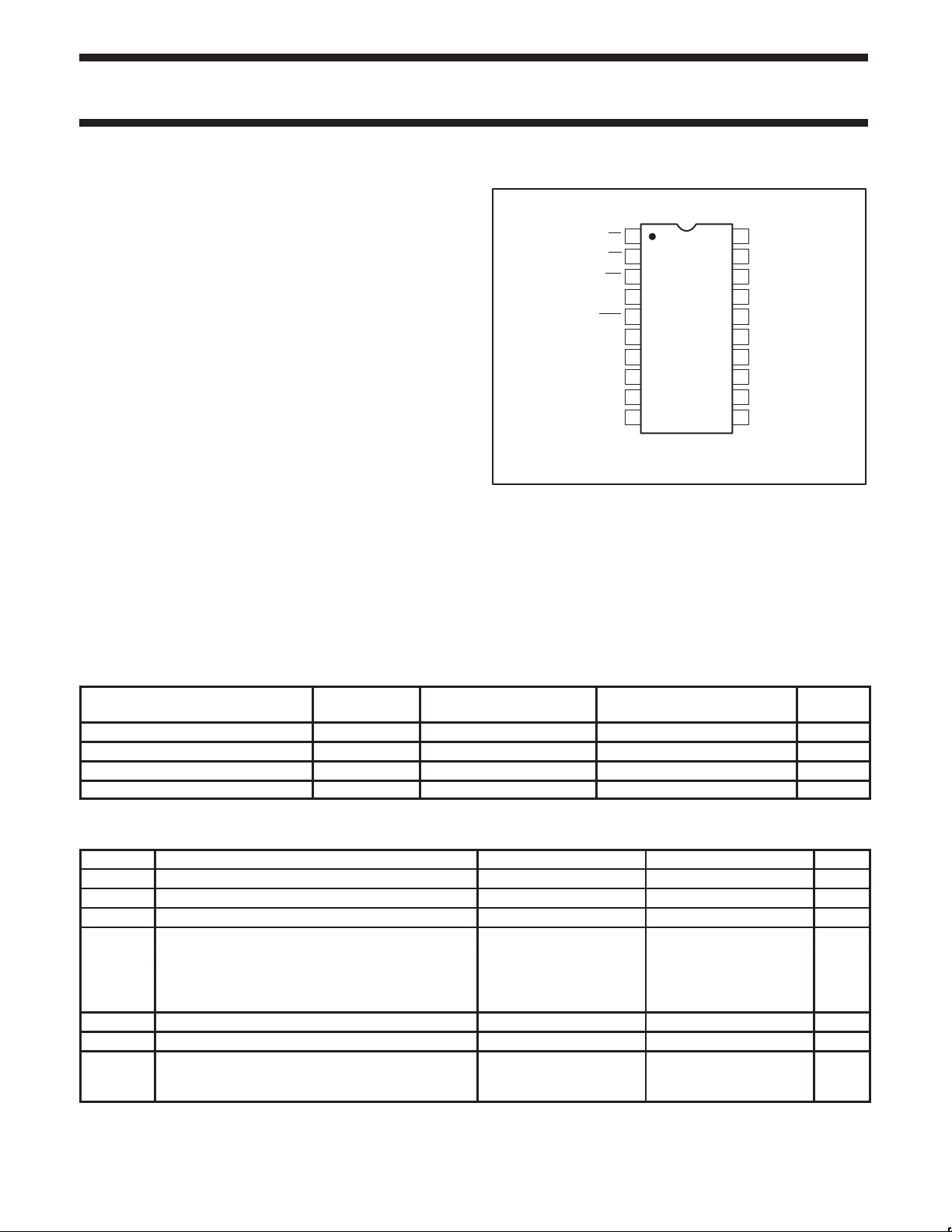
PIN CONFIGURATION
D
N PACKAGES
,
CLK IN
INTR
VIN(+)
V
IN
A GND
V
REF
D GND
CS
RD
WR
1
2
3
4
5
6
7
(–)
8
9
/2
10
TOP VIEW
20
V
19
CLK R
D0
18
17
D1
D2
16
D3
15
D4
14
D5
13
D6
12
D7
11
SL00016
CC
Figure 1. Pin configuration
APPLICATIONS
•Transducer-to-microprocessor interface
•Digital thermometer
•Digitally-controlled thermostat
•Microprocessor-based monitoring and control systems
ORDERING INFORMATION
DESCRIPTION
20-pin plastic small outline (SO) package 0 to 70 °C ADC0803CD, ADC0804CD ADC0803-1CD, ADC0804-1CD SOT163-1
20-pin plastic small outline (SO) package –40 to 85 °C ADC0803LCD, ADC0804LCD ADC0803-1LCD, ADC0804-1LCD SOT163-1
20-pin plastic dual in-line package (DIP) 0 to 70 °C ADC0803CN, ADC0804CN ADC0803-1CN, ADC0804-1CN SOT146-1
20-pin plastic dual in-line package (DIP) –40 to +85 °C ADC0803LCN, ADC0804LCN ADC0803-1LCN, ADC0804-1LCN SOT146-1
TEMPERATURE
RANGE
ORDER CODE TOPSIDE MARKING DWG #
ABSOLUTE MAXIMUM RATINGS
SYMBOL PARAMETER CONDITIONS RATING UNIT
V
CC
T
amb
T
stg
T
sld
P
D
NOTE:
1. Derate above 25 °C, at the following rates: N package at 13.5 mW/°C; D package at 11.1 mW/ °C.
Supply voltage 6.5 V
Logic control input voltages –0.3 to +16 V
All other input voltages –0.3 to (VCC +0.3) V
Operating temperature range
ADC0803LCD/ADC0804LCD –40 to +85 °C
ADC0803LCN/ADC0804LCN –40 to +85 °C
ADC0803CD/ADC0804CD 0 to +70 °C
ADC0803CN/ADC0804CN 0 to +70 °C
Storage temperature –65 to +150 °C
Lead soldering temperature (10 seconds) 230 °C
Maximum power dissipation
1
T
= 25 °C (still air)
amb
N package 1690 mW
D package 1390 mW
2002 Oct 17
2
Page 3
Philips Semiconductors Product data
ADC0803/0804CMOS 8-bit A/D converters
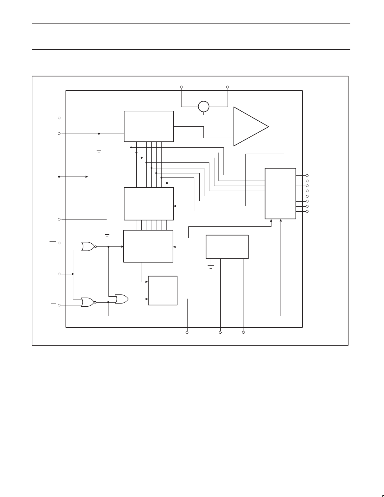
BLOCK DIAGRAM
V
REF
A GND
V
D GND
WR
CC
VIN (+) VIN (–)
+
–
M
9
/2
8
LADDER AND
DECODER
20
SAR
10
3
8–BIT
SHIFT REGISTER
CLOCK
76
+
AUTO ZERO
COMPARATOR
–
OUTPUT
LATCHES
LE OE
D7 (MSB) (11)
D6 (12)
D5 (13)
D4 (14)
D3 (15)
D2 (16)
D1 (17)
D0 (LSB) (18)
CS
RD
1
S
INTR
FF
2
RQ
INTR
5419
CLK IN
CLK R
SL00017
Figure 2. Block diagram
2002 Oct 17
3
Page 4
Philips Semiconductors Product data
SYMBOL
PARAMETER
TEST CONDITIONS
UNIT
VOHLogical “1” output voltage
V
ADC0803/0804CMOS 8-bit A/D converters
DC ELECTRICAL CHARACTERISTICS
V
= 5.0 V, f
CC
R
IN
Control inputs
V
IH
V
IL
I
IH
I
IL
Clock in and clock R
VT+ Clock in positive-going threshold voltage 2.7 3.1 3.5 V
VT– Clock in negative-going threshold voltage 1.5 1.8 2.1 V
V
H
V
OL
V
OH
Data output and INTR
V
OL
I
OZL
I
OZH
I
SC
I
SC
I
CC
NOTES:
1. Analog inputs must remain within the range: –0.05 ≤ V
2. See typical performance characteristics for input resistance at V
3. V
/2 and VIN must be applied after the VCC has been turned on to prevent the possibility of latching.
REF
= 1 MHz, T
CLK
min
≤ T
amb
≤ T
, unless otherwise specified.
max
LIMITS
Min Typ Max
ADC0803 relative accuracy error (adjusted) Full-Scale adjusted 0.50 LSB
ADC0804 relative accuracy error (unadjusted) V
V
/2 input resistance
REF
Analog input voltage range
3
3
/2 = 2.500 V
REF
VCC = 0 V
DC
2
400 680 Ω
1 LSB
–0.05 VCC+0.05 V
DC common-mode error Over analog input voltage range 1/16 1/8 LSB
DC
DC
DC
DC
1
2.0 15 V
1/16 LSB
DC
0.8 V
DC
0.005 1 µA
–1 –0.005 µA
DC
DC
DC
DC
DC
2.4 V
0.4 V
DC
DC
Power supply sensitivity VCC = 5V ±10%
Logical “1” input voltage VCC = 5.25 V
Logical “0” input voltage VCC = 4.75 V
Logical “1” input current VIN = 5 V
Logical “0” input current VIN = 0 V
Clock in hysteresis (VT+)–(VT–) 0.6 1.3 2.0 V
Logical “0” clock R output voltage IOL = 360 µA, VCC = 4.75 V
Logical “1” clock R output voltage IOH = –360 µA, VCC = 4.75 V
Logical “0” output voltage
Data outputs IOL = 1.6 mA, VCC = 4.75 V
INTR outputs IOL = 1.0 mA, VCC = 4.75 V
“
”
p
3-State output leakage V
3-State output leakage V
+Output short-circuit current V
–Output short-circuit current V
Power supply current
IOH = –360 µA, VCC = 4.75 V
IOH = –10 µA, VCC = 4.75 V
= 0 VDC, CS = logical “1” –3 µA
OUT
= 5 VDC, CS = logical “1” 3 µA
OUT
= 0 V, T
OUT
= VCC, T
OUT
f
= 1 MHz, V
CLK
CS
= Logical “1”, T
≤ VCC + 0.05 V.
IN
CC
= 5 V.
= 25 °C 4.5 12 mA
amb
= 25 °C 9.0 30 mA
amb
/2 = OPEN,
REF
= 25 °C
amb
DC
DC
DC
DC
2.4
4.5
3.0 3.5 mA
0.4 V
0.4 V
DC
DC
DC
DC
DC
DC
DC
DC
DC
2002 Oct 17
4
Page 5
Philips Semiconductors Product data
SYMBOL
PARAMETER
TO
FROM
TEST CONDITIONS
UNIT
ADC0803/0804CMOS 8-bit A/D converters
AC ELECTRICAL CHARACTERISTICS
LIMITS
Min Typ Max
CLK
1
= 1 MHz
66 73 µs
0.1 1.0 3.0 MHz
40 60 %
13690 conv/s
70 100 ns
100 150 ns
Conversion time f
f
CLK
Clock frequency
Clock duty cycle
1
1
CR Free-running conversion rate
CLK
CS = 0, f
INTR
= 1 MHz
tied to WR
tW(WR)L Start pulse width CS = 0 30 ns
t
ACC
t1H, t
tW1, t
C
IN
C
OUT
0H
Access time Output RD CS = 0, CL = 100 pF 75 100 ns
3-State control Output RD
INTR delay INTR
R1
WD
or RD
CL = 10 pF, RL = 10 kΩ
See 3-State test circuit
Logic input=capacitance 5 7.5 pF
3-State output capacitance 5 7.5 pF
NOTE:
1. Accuracy is guaranteed at f
= 1 MHz. Accuracy may degrade at higher clock frequencies.
CLK
FUNCTIONAL DESCRIPTION
These devices operate on the Successive Approximation principle.
Analog switches are closed sequentially by successive
approximation logic until the input to the auto-zero comparator
[V
(+)–VIN(–) ] matches the voltage from the decoder . After all bits
IN
are tested and determined, the 8-bit binary code corresponding to
the input voltage is transferred to an output latch. Conversion begins
with the arrival of a pulse at the WR
input if the CS input is low. On
the High-to-Low transition of the signal at the WR or the CS input,
the SAR is initialized, the shift register is reset, and the INTR
output
is set high. The A/D will remain in the reset state as long as the CS
and WR inputs remain low. Conversion will start from one to eight
clock periods after one or both of these inputs makes a Low-to-High
transition. After the conversion is complete, the INTR
pin will make a
High-to-Low transition. This can be used to interrupt a processor, or
otherwise signal the availability of a new conversion result. A read
(RD
) operation (with CS low) will clear the INTR line and enable the
output latches. The device may be run in the free-running mode as
described later. A conversion in progress can be interrupted by
issuing another start command.
Digital Control Inputs
The digital control inputs (CS, WR, RD) are compatible with
standard TTL logic voltage levels. The required signals at these
inputs correspond to Chip Select, STAR T Conversion, and Output
Enable control signals, respectively. They are active-Low for easy
interface to microprocessor and microcontroller control buses. For
applications not using microprocessors, the CS
grounded and the A/D STAR T function is achieved by a
negative-going pulse to the WR
input (Pin 3). The Output Enable
function is achieved by a logic low signal at the RD
which may be grounded to constantly have the latest conversion
present at the output.
input (Pin 1) can be
input (Pin 2),
ANALOG OPERATION
Analog Input Current
The analog comparisons are performed by a capacitive charge
summing circuit. The input capacitor is switched between V
and V
, while reference capacitors are switched between taps on
IN(–)
IN(+)
4
the reference voltage divider string. The net charge corresponds to
the weighted difference between the input and the most recent total
value set by the successive approximation register.
The internal switching action causes displacement currents to flow
at the analog inputs. The voltage on the on-chip capacitance is
switched through the analog differential input voltage, resulting in
proportional currents entering the V
input and leaving the V
IN(+)
IN(–)
input. These transient currents occur at the leading edge of the
internal clock pulses. They decay rapidly so do not inherently cause
errors as the on-chip comparator is strobed at the end of the clock
period.
Input Bypass Capacitors and Source Resistance
Bypass capacitors at the input will average the charges mentioned
above, causing a DC and an AC current to flow through the output
resistance of the analog signal sources. This charge pumping action
is worse for continuous conversions with the V
scale. This current can be a few microamps, so bypass capacitors
should NOT be used at the analog inputs of the V
high resistance sources (> 1 kΩ). If input bypass capacitors are
desired for noise filtering and a high source resistance is desired to
minimize capacitor size, detrimental effects of the voltage drop
across the input resistance can be eliminated by adjusting the full
scale with both the input resistance and the input bypass capacitor
in place. This is possible because the magnitude of the input current
is a precise linear function of the differential voltage.
input at full
IN(+)
REF
/2 input for
2002 Oct 17
5
Page 6

Philips Semiconductors Product data
ADC0803/0804CMOS 8-bit A/D converters
Large values of source resistance where an input bypass capacitor
is not used will not cause errors as the input currents settle out prior
to the comparison time. If a low pass filter is required in the system,
use a low valued series resistor (< 1 kΩ) for a passive RC section or
add an op amp active filter (low pass). For applications with source
resistances at or below 1 kΩ, a 0.1 µF bypass capacitor at the inputs
will prevent pickup due to series lead inductance or a long wire. A
100 Ω series resistor can be used to isolate this capacitor (both the
resistor and capacitor should be placed out of the feedback loop)
from the output of the op amp, if used.
Analog Differential Voltage Inputs and
Common-Mode Rejection
These A/D converters have additional flexibility due to the analog
differential voltage input. The V
input (Pin 7) can be used to
IN(–)
subtract a fixed voltage from the input reading (tare correction). This
is also useful in a 4/20 mA current loop conversion. Common-mode
noise can also be reduced by the use of the differential input.
The time interval between sampling V
IN(+)
and V
is 4.5 clock
IN(–)
periods. The maximum error due to this time difference is given by:
V(max) = (V
) (2fCM) (4.5/f
P
CLK
),
where:
V = error voltage due to sampling delay
V
= peak value of common-mode voltage
P
f
= common mode frequency
CM
For example, with a 60 Hz common-mode frequency, f
1 MHz A/D clock, f
would allow a common-mode voltage, V
[V(max) (f
+
V
P
(2f
, keeping this error to 1/4 LSB (about 5 mV)
CM
CLK
)(4.5)
CLK
)
, which is given by:
P
cm
, and a
or
*3
V
+
P
(5 x 10
(6.28) (60) (4.5)
)(104)
+ 2.95V
The allowed range of analog input voltages usually places more
severe restrictions on input common-mode voltage levels than this,
however.
An analog input span less than the full 5 V capability of the device,
together with a relatively large zero offset, can be easily handled by
use of the differential input. (See Reference Voltage Span Adjust).
Noise and Stray Pickup
The leads of the analog inputs (Pins 6 and 7) should be kept as
short as possible to minimize input noise coupling and stray signal
pick-up. Both EMI and undesired digital signal coupling to these
inputs can cause system errors. The source resistance for these
inputs should generally be below 5 kΩ to help avoid undesired noise
pickup. Input bypass capacitors at the analog inputs can create
errors as described previously. Full scale adjustment with any input
bypass capacitors in place will eliminate these errors.
Reference Voltage
For application flexibility , these A/D converters have been designed
to accommodate fixed reference voltages of 5V to Pin 20 or 2.5 V to
Pin 9, or an adjusted reference voltage at Pin 9. The reference can
be set by forcing it at V
supply voltage (Pin 20). Figure 6 indicates how this is accomplished.
/2 input, or can be determined by the
REF
Reference Voltage Span Adjust
Note that the Pin 9 (V
to the V
forced at the V
supply pin, or is equal to the voltage which is externally
CC
REF
references and full span voltages, this also allows for a ratiometric
voltage reference. The internal gain of the V
the full-scale differential input voltage twice the voltage at Pin 9.
For example, a dynamic voltage range of the analog input voltage
that extends from 0 to 4 V gives a span of 4 V (4–0), so the V
voltage can be made equal to 2 V (half of the 4 V span) and full
scale output would correspond to 4 V at the input.
On the other hand, if the dynamic input voltage had a range of
0.5 to 3.5 V , the span or dynamic input range is 3 V (3.5–0.5). To
encode this 3 V span with 0.5 V yielding a code of zero, the
minimum expected input (0.5 V, in this case) is applied to the V
pin to account for the offset, and the V
span, or 1.5 V. The A/D converter will now encode the V
between 0.5 and 3.5 V with 0.5 V at the input corresponding to a
code of zero and 3.5 V at the input producing a full scale output
code. The full 8 bits of resolution are thus applied over this reduced
input voltage range. The required connections are shown in
Figure 7.
/2) voltage is either 1/2 the voltage applied
REF
/2 pin. In addition to allowing for flexible
/2 input is 2, making
REF
/2 pin is set to 1/2 the 3 V
REF
REF
(+) signal
IN
/2
(–)
IN
Operating Mode
These converters can be operated in two modes:
1) absolute mode
2) ratiometric mode
In absolute mode applications, both the initial accuracy and the
temperature stability of the reference voltage are important factors in
the accuracy of the conversion. For V
/2 voltages of 2.5 V , initial
REF
errors of ±10 mV will cause conversion errors of ±1 LSB due to the
gain of 2 at the V
value and stability of the V
important as the same error is a larger percentage of the V
/2 input. In reduced span applications, the initial
REF
/2 input voltage become even more
REF
REF
/2
nominal value. See Figure 8.
In ratiometric converter applications, the magnitude of the reference
voltage is a factor in both the output of the source transducer and
the output of the A/D converter, and, therefore, cancels out in the
final digital code. See Figure 9.
Generally , the reference voltage will require an initial adjustment.
Errors due to an improper reference voltage value appear as
full-scale errors in the A/D transfer function.
ERRORS AND INPUT SPAN ADJUSTMENTS
There are many sources of error in any data converter, some of
which can be adjusted out. Inherent errors, such as relative
accuracy, cannot be eliminated, but such errors as full-scale and
zero scale offset errors can be eliminated quite easily . See Figure 7.
Zero Scale Error
Zero scale error of an A/D is the difference of potential between the
ideal 1/2 LSB value (9.8 mV for V
voltage which just causes an output transition from code 0000 0000
to a code of 0000 0001.
If the minimum input value is not ground potential, a zero offset can
be made. The converter can be made to output a digital code of
0000 0000 for the minimum expected input voltage by biasing the
(–) input to that minimum value expected at the VIN(–) input to
V
IN
that minimum value expected at the V
differential mode of the converter . Any offset adjustment should be
done prior to full scale adjustment.
/2=2.500 V) and that input
REF
(+) input. This uses the
IN
2002 Oct 17
6
Page 7

Philips Semiconductors Product data
ADC0803/0804CMOS 8-bit A/D converters
Full Scale Adjustment
Full scale gain is adjusted by applying any desired offset voltage to
V
(–), then applying the VIN(+) a voltage that is 1-1/2 LSB less than
IN
the desired analog full-scale voltage range and then adjusting the
magnitude of V
/2 input connection) for a digital output code which just
V
REF
changes from 111 1 11 10 to 11 11 1111. The ideal V
this full-scale adjustment is given by:
()) + VIN(*) * 1.5 x
V
IN
where:
V
= high end of analog input range (ground referenced)
MAX
V
= low end (zero offset) of analog input (ground referenced)
MIN
/2 input voltage (or the VCC supply if there is no
REF
(+) voltage for
IN
* V
V
MAX
MIN
255
CLOCKING OPTION
The clock signal for these A/Ds can be derived from external
sources, such as a system clock, or self-clocking can be
accomplished by adding an external resistor and capacitor, as
shown in Figure 11.
Heavy capacitive or DC loading of the CLK R pin should be avoided
as this will disturb normal converter operation. Loads less than 50pF
are allowed. This permits driving up to seven A/D converter CLK IN
pins of this family from a single CLK R pin of one converter. For
larger loading of the clock line, a CMOS or low power TTL buffer or
PNP input logic should be used to minimize the loading on the CLK
R pin.
Restart During a Conversion
A conversion in process can be halted and a new conversion began
by bringing the CS
them to go high again. The output data latch is not updated if the
conversion in progress is not completed; the data from the
previously completed conversion will remain in the output data
latches until a subsequent conversion is completed.
and WR inputs low and allowing at least one of
Continuous Conversion
To provide continuous conversion of input data, the CS and RD
inputs are grounded and INTR output is tied to the WR input. This
INTR
/WR connection should be momentarily forced to a logic low
upon power-up to insure circuit operation. See Figure 10 for one
way to accomplish this.
DRIVING THE DATA BUS
This CMOS A/D converter, like MOS microprocessors and
memories, will require a bus driver when the total capacitance of the
data bus gets large. Other circuitry tied to the data bus will add to
the total capacitive loading, even in the high impedance mode.
There are alternatives in handling this problem. The capacitive
loading of the data bus slows down the response time, although DC
specifications are still met. For systems with a relatively low CPU
clock frequency, more time is available in which to establish proper
logic levels on the bus, allowing higher capacitive loads to be driven
(see Typical Performance Characteristics).
At higher CPU clock frequencies, time can be extended for I/O
reads (and/or writes) by inserting wait states (8880) or using
clock-extending circuits (6800, 8035).
Finally, if time is critical and capacitive loading is high, external bus
drivers must be used. These can be 3-State buffers (low power
Schottky is recommended, such as the N74LS240 series) or special
higher current drive products designed as bus drivers. High current
bipolar bus drivers with PNP inputs are recommended as the PNP
input offers low loading of the A/D output, allowing better response
time.
POWER SUPPLIES
Noise spikes on the VCC line can cause conversion errors as the
internal comparator will respond to them. A low inductance filter
capacitor should be used close to the converter V
of 1 µF or greater are recommended. A separate 5 V regulator for
the converter (and other 5 V linear circuitry) will greatly reduce
digital noise on the V
supply and the attendant problems.
CC
pin and values
CC
WIRING AND LAYOUT PRECAUTIONS
Digital wire-wrap sockets and connections are not satisfactory for
breadboarding this (or any) A/D converter. Sockets on PC boards
can be used. All logic signal wires and leads should be grouped or
kept as far as possible from the analog signal leads. Single wire
analog input leads may pick up undesired hum and noise, requiring
the use of shielded leads to the analog inputs in many applications.
A single-point analog ground separate from the logic or digital
ground points should be used. The power supply bypass capacitor
and the self-clocking capacitor, if used, should be returned to digital
ground. Any V
and any input shielding should be returned to the analog ground
point. Proper grounding will minimize zero-scale errors which are
present in every code. Zero-scale errors can usually be traced to
improper board layout and wiring.
/2 bypass capacitor, analog input filter capacitors,
REF
2002 Oct 17
7
Page 8

Philips Semiconductors Product data
ADC0803/0804CMOS 8-bit A/D converters
APPLICATIONS
Microprocessor Interfacing
This family of A/D converters was designed for easy microprocessor
interfacing. These converters can be memory mapped with
appropriate memory address decoding for CS
active-Low write pulse from the processor is then connected to the
WR
input of the A/D converter, while the processor active-Low read
pulse is fed to the converter RD
the clock signal is derived from the microprocessor system clock,
the designer/programmer should be sure that there is no attempt to
read the converter until 74 converter clock pulses after the start
pulse goes high. Alternatively, the INTR
the processor to cause reading of the converted data. Of course, the
converter can be connected and addressed as a peripheral (in I/O
space), as shown in Figure 12. A bus driver should be used as a
buffer to the A/D output in large microprocessor systems where the
data leaves the PC board and/or must drive capacitive loads in
excess of 100 pF. See Figure 14.
Interfacing the SCN8048 microcomputer family is pretty simple, as
shown in Figure 13. Since the SCN8048 family has 24 I/O lines, one
of these (shown here as bit 0 or port 1) can be used as the chip
select signal to the converter, eliminating the need for an address
decoder. The RD
and writing to a dummy address.
and WR signals are generated by reading from
input to read the converted data. If
(read) input. The
pin may be used to interrupt
Digitizing a Transducer Interface Output
Circuit Description
Figure 15 shows an example of digitizing transducer interface output
voltage. In this case, the transducer interface is the NE5521, an
LVDT (Linear Variable Differential Transformer) Signal Conditioner.
The diode at the A/D input is used to insure that the input to the A/D
does not go excessively beyond the supply voltage of the A/D. See
the NE5521 data sheet for a complete description of the operation of
that part.
Circuit Adjustment
To adjust the full scale and zero scale of the A/D, determine the range
of voltages that the transducer interface output will take on. Set the
LVDT core for null and set the Zero Scale Scale Adjust Potentiometer
for a digital output from the A/D of 1000 000. Set the LVDT core for
maximum voltage from the interface and set the Full Scale Adjust
potentiometer so the A/D output is just barely 111 1 11 11.
A Digital Thermostat
Circuit Description
The schematic of a Digital Thermostat is shown in Figure 16. The
A/D digitizes the output of the LM35, a temperature transducer IC
with an output of 10 mV per °C. With V
10 mV corresponds to 1/2 LSB and the circuit resolution is 2 °C.
Reducing V
lower V
The desired temperature is set by holding either of the set buttons
closed. The SCC80C451 programming could cause the desired
(set) temperature to be displayed while either button is depressed
and for a short time after it is released. At other times the ambient
temperature could be displayed.
The set temperature is stored in an SCN8051 internal register. The
A/D conversion is started by writing anything at all to the A/D with
port pin P10 set high. The desired temperature is compared with the
digitized actual temperature, and the heater is turned on or off by
clearing setting port pin P12. If desired, another port pin could be
used to turn on or off an air conditioner.
The display drivers are NE587s if common anode LED displays are
used. Of course, it is possible to interface to LCD displays as well.
/2 to 1.28 yields a resolution of 1 °C. Of course, the
REF
/2 is, the more sensitive the A/D will be to noise.
REF
/2 set for 2.56 V, this
REF
2002 Oct 17
8
Page 9

Philips Semiconductors Product data
ADC0803/0804CMOS 8-bit A/D converters
TYPICAL PERFORMANCE CHARACTERISTICS
Power Supply Current vs
Temperature
3.2
f
= 1 MHz
3.0
2.8
2.6
2.4
2.2
POWER SUPPLY CURRENT (mA)
2.0
1.8
–50 –25 0 25 50 75 100 125
AMBIENT TEMPERATURE (°C)
CLK
CS = H
Logic Input Threshold
Voltage vs Supply Voltage
1.70
1.60
1.50
LOGIC INPUT (V)
1.40
1.30
4.50 4.75 5.00 5.25 5.50
VCC SUPPLY VOLTAGE (V)
5.5 V
5.0 V
4.5 V
–55 °C
+25 °C
+125 °C
Clock Frequency vs
Clock Capacitor
10.0
8.0
6.0
4.0
2.0
1.0
0.8
0.6
CLOCK FRQ (MHz)
0.4
0.2
0.1
10 20 40 60 80100 200 400 6001000
MAX.
TYP.
MIN.
CLOCK CAP (pF)
CLK–IN Threshold Voltage vs
Supply Voltage
4.5
–55 °C ≤ T
4.0
3.5
3.0
2.5
2.0
1.5
CLK–IN THRESHOLD VOLTAGE (V)
1.0
4.50 4.75 5.00 5.25 5.50
≤ 125 °C
amb
V
T+
V
T
VCC SUPPLY VOLTAGE (V)
Input Current vs
Applied Voltage at V
5
4
3
2
1
0
–1
REF/2
f (mA)
–2
–3
–4
–5
VCC = 5.0 V
T
= 25 oC
amb
01234
APPLIED V
REF/2
REF/2
(V)
Output Current vs
Temperature
18
16
14
12
10
OUTPUT CURRENT (mA)
8
6
–50 –25 0 25 50 75 100 125
VCC = 5.0 V
VO = 0.4 V
AMBIENT TEMPERATURE (
Pin
VO = 2.5 V
o
C)
5
2002 Oct 17
Full Scale Error vs
4
3
2
ERROR (LSB)
1
0
Conversion Time
VCC = 5.0 V
V
REF/2 = 2.5 V
0 20 40 60 80 100 120
CONVERSION TIME (µs)
Figure 3. Typical Performance Characteristics
Delay From RD
Falling
Edge to Data Valid vs
Load Capacitance
VCC = 5.0 V
= 25 oC
T
amb
0 200 400 600 800 1000
LOAD CAPACITANCE (pF)
SL00018
DEALY (ns)
350
300
250
200
150
100
50
0
9
Page 10

Philips Semiconductors Product data
ADC0803/0804CMOS 8-bit A/D converters
3-STATE TEST CIRCUITS AND WA VEFORMS (ADC0801-1)
20ns
t
CC
OH
r
10%
90%
50%
90%
t
1H
RD
CS
V
CC
C
10 pF
t
1H
DATA
OUTPUT
L
10 kΩ
DATA
OUTPUT
RD
V
GND
V
GND
Figure 4. 3-State Test Circuits and Waveforms (ADC0801-1)
TIMING DIAGRAMS (All timing is measured from the 50% voltage points)
START
CONVERSION
CS
RD
CS
V
V
CC
CC
10 kΩ
DATA
C
t
OH
OUTPUT
L
10 pF
DATA
OUTPUT
RD
V
CC
GND
V
OH
GND
t
r
50%
10%
90%
SL00019
10%
t
0H
WR
ACTUAL INTERNAL
STATUS OF THE
CONVERTER
INTR
t
WI
(LAST DATA WAS READ)
(LAST DATA WAS NOT READ)
INTR
CS
RD
DATA
OUTPUTS
t
W(WR)L
INTR
RESET
NOTE
1 TO 8 X 1/f
t
RI
t
ACC
”NOT BUSY”
CLK
”BUSY”
THREE–STATE
t
1H, t0H
INTERNAL T
DATA IS VALID IN
OUTPUT LATCHES
C
INT ASSERTED
1/2 T
CLK
NOTE:
Read strobe must occur 8 clock periods (8/f
2002 Oct 17
Output Enable and Reset INTR
) after assertion of interrupt to guarantee reset of INTR.
CLK
Figure 5. Timing Diagrams
SL00020
10
Page 11

Philips Semiconductors Product data
ADC0803/0804CMOS 8-bit A/D converters
V
CC
V
20
REF
R
9
V
/2
REF
DIGITAL
CIRCUITS
R
810
ANALOG
CIRCUITS
(5V)
V
REF
ZS
OFFSET
ADJUST
FS
OFFSET
ADJUST
–
+
330 Ω
0.1 µF
TO V
TO V
IN
SL00022
REF
/2
(–)
Figure 7. Offsetting the Zero Scale and Adjusting the Input
Range (Span)
NOTE:
The V
/2 voltage is either 1/2 the VCC voltage or is that which is forced at Pin 9.
REF
Figure 6. Internal Reference Design
+5V
V
CC
REF
/2
+
10 µF
VOLTAGE
REFERENCE
/2
V
REF
VIN(+)
V
IN
A/D
V
(–)
a. Fixed Reference
SL00021
+5V
V
CC
VIN(+)
A/D
VIN(–)
b. Fixed Reference Derived from V
+
10 µF
V
/2
REF
CC
Figure 8. Absolute Mode of Operation
2 kΩ
+5V
2 kΩ
100 Ω
2 kΩ2 kΩ
c. Optional Full
Scale Adjustment
SL00023
2002 Oct 17
11
Page 12

Philips Semiconductors Product data
ADC0803/0804CMOS 8-bit A/D converters
V
CC
(+)
V
TRANSDUCER
IN
A/D
V
(–)
IN
Figure 9. Ratiometric Mode of Operation with Optional Full
Scale Adjustment
V
CC
+
10µF
2 kΩ
V
/2
REF
FULL SCALE
OPTIONAL
100 Ω
2 kΩ
SL00024
10 kΩ
10 kΩ
CLK R
19
R
CLK IN 4
C
CLK
A/D
Figure 11. Self-Clocking the Converter
+5 V
47 µF TO
100 µF
2.7 kΩ
56 pF
CLK IN
VIN(+)
VIN(–)
A GND
V
REF
D GND
CS
RD
WR
INTR
/2
10
10k
1
2
3
4
5
6
7
8
9
A/D
Figure 10. Connection for Continuous Conversion
f
= 1/1.7 R C
CLK
R = 10 kΩ
SL00026
ANALOG
INPUTS
20
19
18
17
16
15
14
13
12
11
56 pF
V
CC
CLK R
D0
DB0
D1
DB1
D2
DB2
D3
DB3
D4
DB4
D5
DB5
D6
DB6
D7
DB7
SL00025
CLK IN
V
D GND
+5 V
CS
RD
WR
INTR
VIN(+)
V
IN
A GND
REF
INT
I/O WR
I/O RD
V
CC
CLK R
D0
DB0
D1
DB1
D2
DB2
D3
DB3
D4
DB4
D5
DB5
D6
DB6
D7
DB7
ADDRESS
+5 V
10 kΩ
1
2
3
4
5
A/D
6
7
(–)
8
/2
9
10
DECODE
LOGIC
20
19
18
17
16
15
14
13
12
11
2002 Oct 17
SL00027
Figure 12. Interfacing to 8080A Microprocessor
12
Page 13

Philips Semiconductors Product data
ADC0803/0804CMOS 8-bit A/D converters
V
CC
40
SCN8051
OR
SCN80C51
+5 V
V
CC
P1.0
1
P1.1
2
P1.2
3
P1.3
4
P1.4
5
P1.5
6
P1.6
7
P1.7
8
17 RD
16
WR
12
INTO
39
P0.0
D0
D1
D2
D3
D4
D5
D6
D7
WR
INTR
CS
RD
18
17
16
15
14
13
12
11
2
3
5
1
20
A/D
Figure 13. SCN8051 Interfacing
19 CLK R
4 CLK IN
VIN(+)
6
V
REF
7
A GND
12
D GND
11
18
D0
17
D1
16
D2
15
D3
14
D4
13
10 kΩ
56 pF
ANALOG
INPUTS
/2
Figure 14. Buffering the A/D Output to Drive High Capacitance
A/D
D5
12
D6
11
D7
8–BIT
BUFFER
N74LS241
N74LS244
N74LS541
DATA
OE
SL00029
BUS
Loads and for Driving Off-Board Loads
SL00028
+5 V
C
t
4.7 kΩ
4.7 kΩ
1.5 kΩ
1µF
0.47 µF
18 kΩ
820 Ω
22 kΩ
470 Ω
3.3 kΩ
2 kΩ
NE5521
IN4148
VIN(+)
V
IN
V
CC
A/D
(–)
Figure 15. Digitizing a Transducer Interface Output
LVDT
V
REF
+5 V
2 kΩ
/2
100 Ω
2 kΩ
FULL SCALE
ADJUST
SL00030
2002 Oct 17
13
Page 14

Philips Semiconductors Product data
ADC0803/0804CMOS 8-bit A/D converters
5
RBI
6
2
1/4
HEF4071
1
NE587
7
3
7
8
+V
LOWER
RAISE
2N3906
P15
P16
13 14
SCC80C51
20 GND29 P12
1/4
HEF4071
18
DB0
17
DB1
16
DB2
15
DB3
14
DB4
13
DB5
12
DB6
11
DB7
8RD
10
WR
INT
6
27
P10
RBO 4
RBI 5
6
2
1
NE587
7
3
D0
18
D1
17
D2
16
D3
15
D4
14
D5
13
D6
12
D7
11
2
RD
3
WR
INTR
5
CS
1
D GND 10 8 AGND
A/D
7
8
20
19
4
6
7
10 kΩ
10 kΩ
V
CC
CLK R
10 kΩ
CLK IN
56 pF
V
IN
VIN(–)
+5 V
+
10 µF
(+)
LM35
2002 Oct 17
1N4148
TO HEATER
SL00031
Figure 16. Digital Thermostat
14
Page 15

Philips Semiconductors Product data
ADC0803/0804CMOS 8-bit A/D converters
SO20: plastic small outline package; 20 leads; body width 7.5 mm SOT163-1
2002 Oct 17
15
Page 16

Philips Semiconductors Product data
ADC0803/0804CMOS 8-bit A/D converters
DIP20: plastic dual in-line package; 20 leads (300 mil) SOT146-1
2002 Oct 17
16
Page 17

Philips Semiconductors Product data
ADC0803/0804CMOS 8-bit A/D converters
REVISION HISTORY
Rev Date Description
_3 20021017 Product data; third version; supersedes data of 2001 Aug 03.
Engineering Change Notice 853–0034 28949 (date: 20020916).
Modifications:
•Add “Topside Marking” column to Ordering Information table.
_2 20010803 Product data; second version (9397 750 08926).
Engineering Change Notice 853–0034 26832 (date: 20010803).
_1 19940831 Product data; initial version.
Engineering Change Notice 853–0034 13721 (date: 19940831).
2002 Oct 17
17
Page 18

Philips Semiconductors Product data
ADC0803/0804CMOS 8-bit A/D converters
Data sheet status
Level
I
Data sheet status
Objective data
[1]
Product
[2] [3]
status
Development
Definitions
This data sheet contains data from the objective specification for product development.
Philips Semiconductors reserves the right to change the specification in any manner without notice.
II
III
[1] Please consult the most recently issued data sheet before initiating or completing a design.
[2] The product status of the device(s) described in this data sheet may have changed since this data sheet was published. The latest information is available on the Internet at URL
[3] For data sheets describing multiple type numbers, the highest-level product status determines the data sheet status.
Preliminary data
Product data
http://www.semiconductors.philips.com.
Qualification
Production
This data sheet contains data from the preliminary specification. Supplementary data will be published
at a later date. Philips Semiconductors reserves the right to change the specification without notice, in
order to improve the design and supply the best possible product.
This data sheet contains data from the product specification. Philips Semiconductors reserves the
right to make changes at any time in order to improve the design, manufacturing and supply. Relevant
changes will be communicated via a Customer Product/Process Change Notification (CPCN).
Definitions
Short-form specification — The data in a short-form specification is extracted from a full data sheet with the same type number and title. For detailed information see
the relevant data sheet or data handbook.
Limiting values definition — Limiting values given are in accordance with the Absolute Maximum Rating System (IEC 60134). Stress above one or more of the limiting
values may cause permanent damage to the device. These are stress ratings only and operation of the device at these or at any other conditions above those given
in the Characteristics sections of the specification is not implied. Exposure to limiting values for extended periods may affect device reliability.
Application information — Applications that are described herein for any of these products are for illustrative purposes only. Philips Semiconductors make no
representation or warranty that such applications will be suitable for the specified use without further testing or modification.
Disclaimers
Life support — These products are not designed for use in life support appliances, devices, or systems where malfunction of these products can reasonably be
expected to result in personal injury . Philips Semiconductors customers using or selling these products for use in such applications do so at their own risk and agree
to fully indemnify Philips Semiconductors for any damages resulting from such application.
Right to make changes — Philips Semiconductors reserves the right to make changes in the products—including circuits, standard cells, and/or software—described
or contained herein in order to improve design and/or performance. When the product is in full production (status ‘Production’), relevant changes will be communicated
via a Customer Product/Process Change Notification (CPCN). Philips Semiconductors assumes no responsibility or liability for the use of any of these products, conveys
no license or title under any patent, copyright, or mask work right to these products, and makes no representations or warranties that these products are free from patent,
copyright, or mask work right infringement, unless otherwise specified.
Contact information
For additional information please visit
http://www.semiconductors.philips.com . Fax: +31 40 27 24825
For sales offices addresses send e-mail to:
sales.addresses@www.semiconductors.philips.com.
Document order number: 9397 750 10538
Koninklijke Philips Electronics N.V. 2002
All rights reserved. Printed in U.S.A.
Date of release: 10-02
2002 Oct 17
18
Page 19

This datasheet has been download from:
www.datasheetcatalog.com
Datasheets for electronics components.
 Loading...