

Page 1

PCH3582/3782/3982
User Manual
PCH3582/3782/3982: 15/17/19” Industrial Fanless Panel PC
with Atom D525 processor
14628 Central Ave,
Chin o, CA 91710
tel: 909.597.7588, fax:909.597.1939
15/17/19 inch Atom Fanless Panel PC
© Copyrigh t 2013 Acnodes, Inc.
All rights reserv ed. Product descrip tion and product specification s
are subj ect to ch ange wi thout not ice . For l atest product
in format ion, please visit Acnode s’ web site at www.acnode s.com .
Page 2

Warning!_______________________________
This equipment generates, uses and can radiate radio frequency energy and if not installed and
used in accordance with the instructions manual, it may cause interference to radio
communications.
It has been tested and found to comply with the limits for a Class A computing device pursuant to
FCC Rules, which are designed to provide reasonable protection against such interference when
operated in a commercial environment. Operation of this equipment in a residential area is likely to
cause interference in which case the user at his own expense will be required to take whatever
measures may be required to correct the interference.
Electric Shock Hazard – Do not operate the machine with its back cover removed. There are
dangerous high voltages inside.
Page 3

Packing List
Accessories (as ticked) included in this package are:
□
AC power cable
□
Driver & manual CD disc
□
Other._ (please specify)
Safety Precautions
Follow the messages below to avoid your systems from damage:
◆
Avoid your system from static electricity on all occasions.
◆
Prevent electric shock. Don’t touch any components of this card when the card is
power-on. Always disconnect power when the system is not in use.
◆
Disconnect power when you change any hardware devices. For instance, when you
connect a jumper or install any cards, a surge of power may damage the electronic
components or the whole system.
Page 4

Table of Contents
Warning
Packing List...................................................................................................................3
Safety Precautions........................................................................................................3
!…
………………………………………………………………………….……..….2
Chapter 1 Getting Started
1.1 Specifications………………………………………….………….……...…..6
1.2 Dimensions…………………………………...……………….…………......8
1.3 Brief Description of PCH3X82……….………………….………………12
Chapter 2 Hardware Installation
2.1 Mainboard Specifications………………………..…………….…………13
2.2 Jumpers Setting and Connectors………………………….……………17
Chapter 3 BIOS Setup
3.1 Operations after POST Screen.............................................................26
3.2 BIOS SETUP UTILITY................................................. ...............27
3.3 System Overview.......................................................................28
3.4 Advanced Settings................................................................... 29
3.5 Advanced PCI/PnP Settings................................................................ 37
3.6 Boot Settings....................................................................................... 40
3.7 Security Settings.................................................................................. 42
3.8 Advanced Chipset Settings.................................................................. 43
3.9 Exit Options..........................................................................................49
3.10 Examples of GPIO Programming.......................................................50
Chapter 4 Installation of Drivers
Page 5

4.1 Chipset Driver.…………………………...…………………………………59
4.2 GMA 3150 VGA Chipset Driver..…....…......………………..............…..62
4.3 Network adapter Driver……..................................………………….….66
4.4 Realtek HD Audio Driver Installation………………….…………………69
Chapter 5 Touch Screen Installation
5.1 Introduction to Touch Screen Controller Board………………………....72
5.2 Windows 2000/XP USB Driver Installation………………….………..….72
Figures
Figure 1.1: Dimensions of PCH3582…………….....……………………...9
Figure 1.2: Dimensions of PCH3782……………..……...………………..10
Figure 1.3: Dimensions of PCH3982………………………...………………..11
Figure 1.4: Overview of PCH3X82 ……..….………………………...12
Figure 2.1: Mainboard Overview……………………………………..……..…13
Figure 2.2: Mainboard Dimensions……………………………………………13
Figure 2.3: Jumpers and Connectors Location-TOP…………………...……14
Figure 2.4: Jumpers and Connectors Location- Bottom………………….…14
Figure 5.1: Bird‟s Eye View of Control Board…………………………….......72
Page 6

Chapter 1 Getting Started
Model No.
Specs
PCH3582
PCH3782
PCH3982
System
Processor
Atom D525 1.8GHz processor FSB 800MHz
System Chipset
ICH8M Chipset
System Memory
1 x 204 Pin SO-DIMM DDR3 800GHz, up to 2GB SDRAM
Storage
1 x 2 .5" SATA HDD Space
1 x CF Internal Slot
1 x CF External Slot for option (except APC-3282/3283)
External I/O Port
4XUSB 2.0
2XGbE RJ-45 LAN port
1XDB-15 VGA (disable for use)
1XDB-9 RS422/485(default RS-485)
1XDB-9 RS-232
1XDC Power input T/B connector
7 Pin T/B for 2in/out/1Ground/Switch±
Expansion Slots
None
OSD
OSD control
Brightness/ Screen and Touch on/off /Power on/off
(APC-3782/3783/3982/3983 add auto tune function key)
OS support
Windows XP Pro, XP Embedded, Windows Embedded Standard 7
LCD
Display Type
1
15”TFT-LCD
17”TFT-LCD
19”TFT-LCD
Max. Resolution
8
1024x768
1280x1024
1280x1024
Max. Color
262K
Luminance (cd/m2)
3
400
350
350
View Angle
H
:
1
H:160° / V:140° (APC-
3582) H:140° / V:110°
(APC-3583)
H:170° / V:160
°
H:160° / V:160
°
Backlight Lifetime
50,000 hrs
Touch Screen
Type
Resistive Touch
Light Transmission
80%
Power Supply
Power Input
DC 11~32V
1.1 Specifications
Page 7

Mechanical
Construction
Stainless Steel Housing (APC-3X82) / Steel Housing (APC-3X83)
IP Rating
Front Panel IP65 / 6 sides IP42 with waterproof kit
Mounting
VEVESA 75x75
Mount
VESA 75x75
Mount
VESA 100x100
Mount
Dimensions (WxHxD)
33399(W)x324(H)x
67(D) mm
432(W)x358(H)x
66.8(D)mm
470(W)x388.6(H)x
67(D)mm
Environmental
Operating Temperature
0~50 ゚ C
Storage Temperature
-20~60 ゚ C
Storage Humidity
10~90% @40 ゚ C non-condensing
Certificate
CE/FCC Class A
Page 8
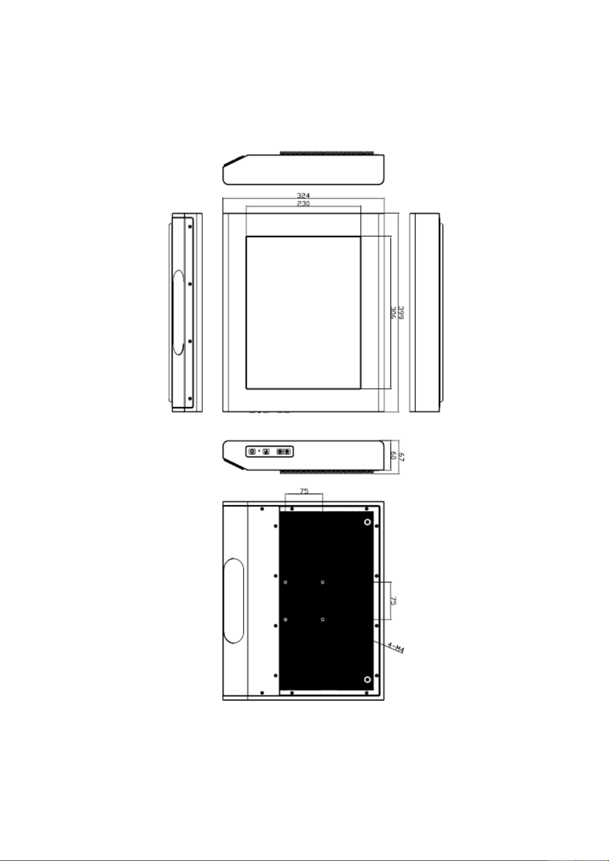
1.2 Dimensions
Figure 1.1: Dimensions of PCH3582
Page 9
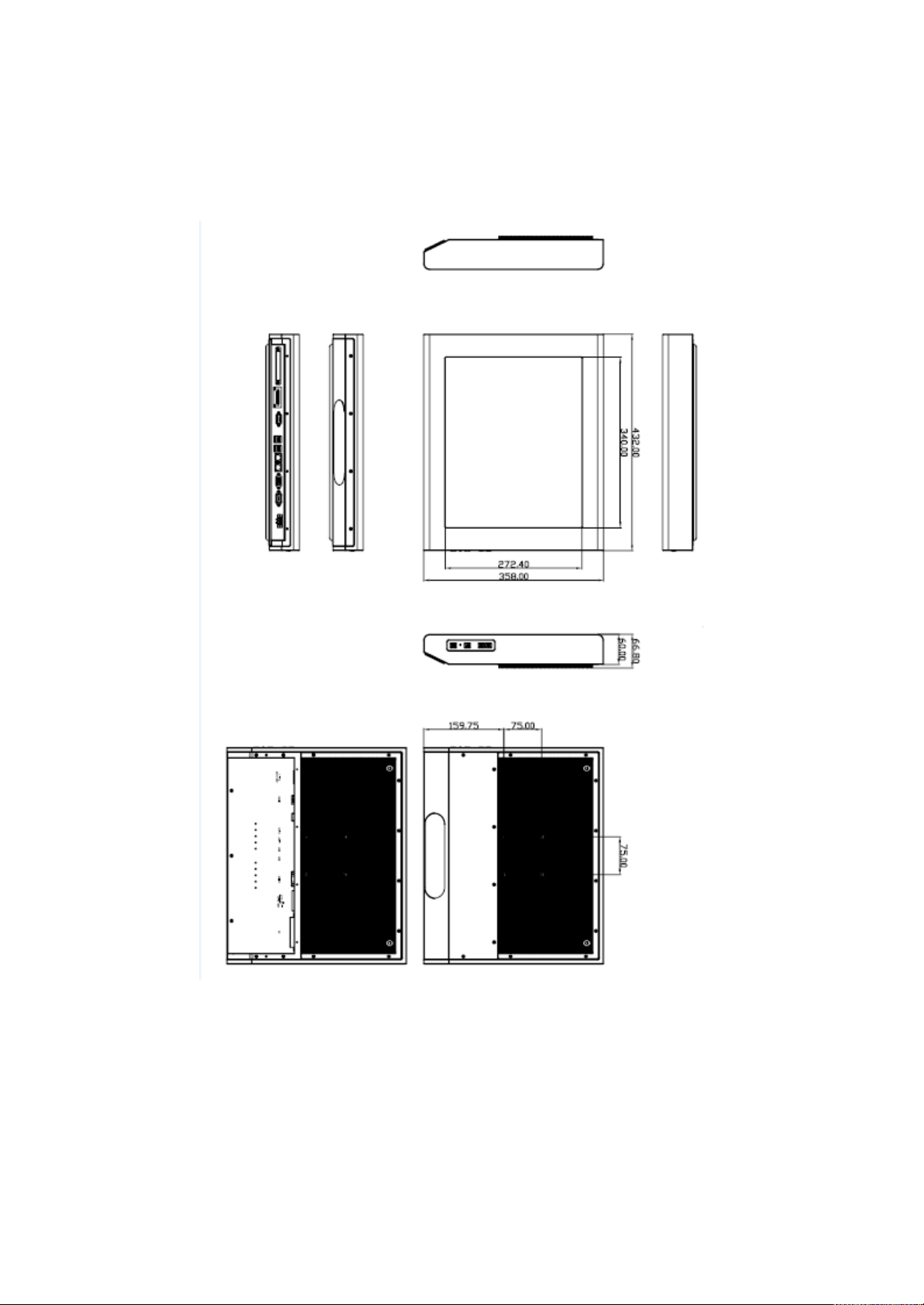
Figure 1.2: Dimensions of PCH3782
Page 10
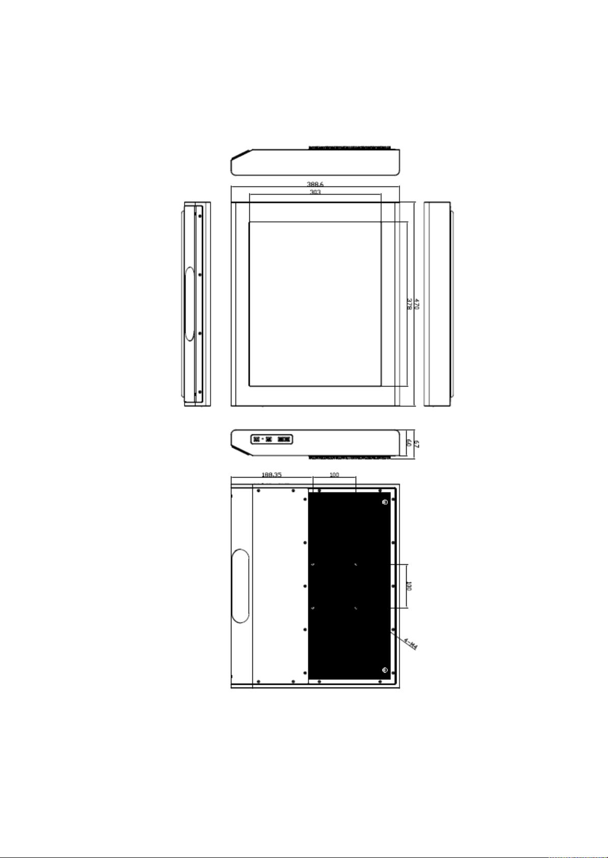
Figure 1.3: Dimensions of PCH3982
Page 11
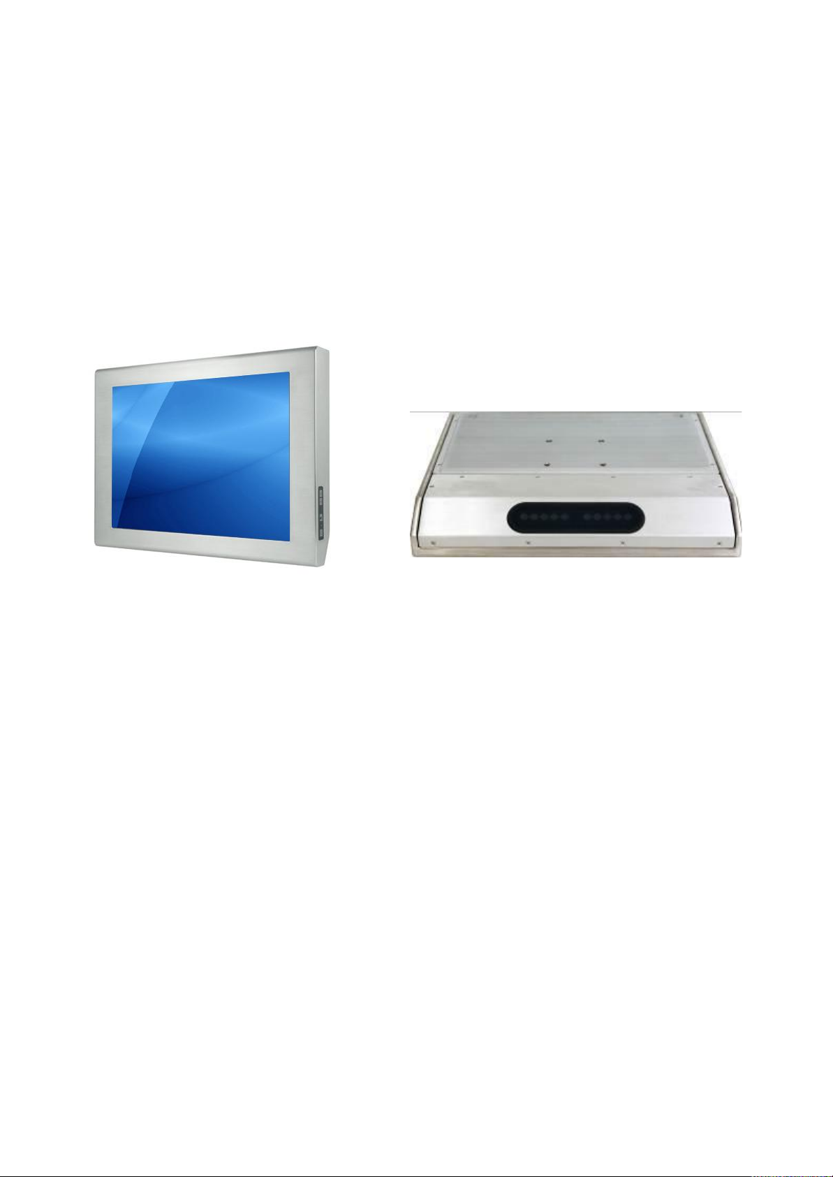
1.3 Brief Description of PCH3X82
The fanless PCH3X82 is Atom D525 powered panel PC with a rich variety of functions and peripherals.
PCH3X82 is designed for easy and simplified integration into various vehicle applications. It
comes with a compact flash slot, 2.5-inch hard disk drive, DDR3 memory, audio jack, 2 Ethernet, DC
input. 4 external USB ports ensure simplified connectivity to a variety of external peripheral
devices. The unit supports Windows XP Pro, XP Embedded and Windows Embedded Standard
7. The fanless touch panel computer is ideal for use as Web Browser, Terminal and HMI at
all levels of automation control.
Figure 1.4: Overview of PCH3X82
Page 12
Chapter 2 Hardware Installation
2.1 Mainboard Specifications
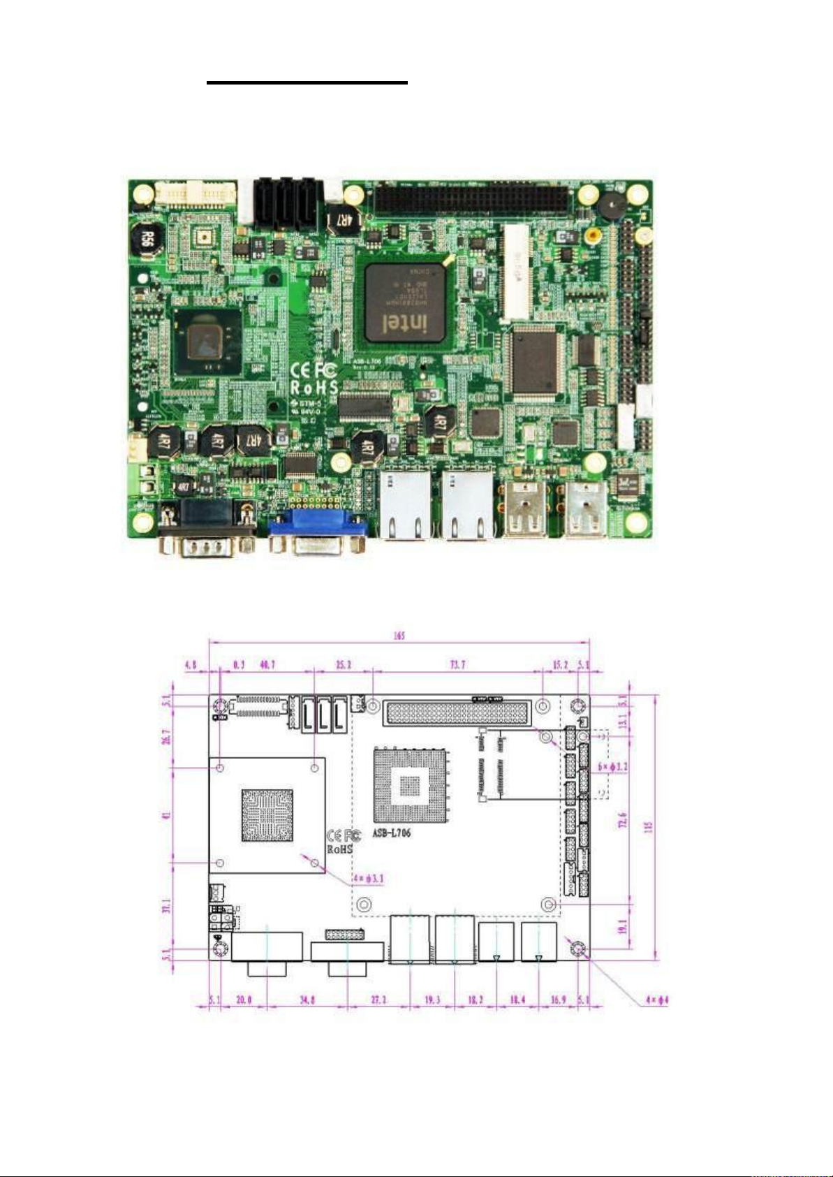
Figure 2.1: Mainboard Overview
Figure 2.2: Mainboard Dimensions
Page 13
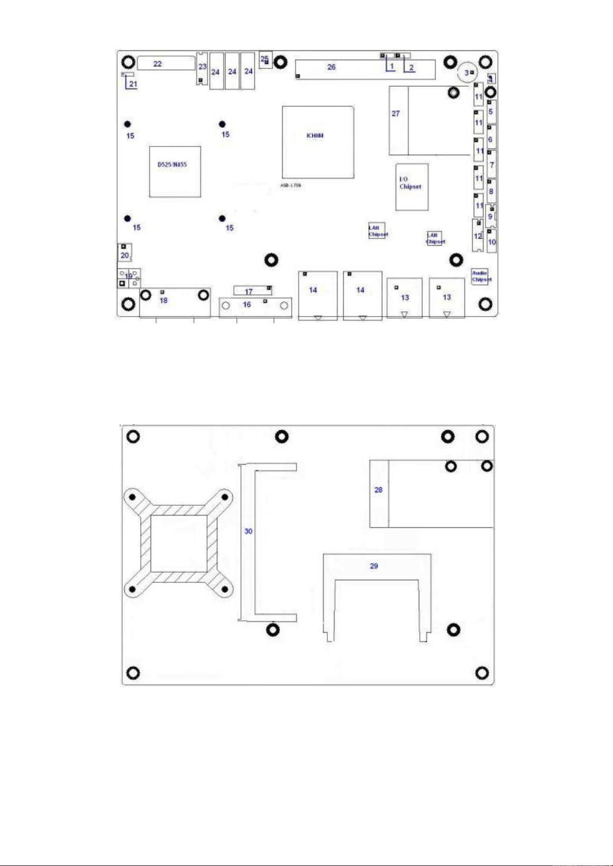
Figure 2.3: Jumpers and Connectors Location-TOP
Figure 2.4: Jumpers and Connectors Location- Bottom
Page 14

Specifications
Board Size 165mm x 115mm
CPU Support Atom D525 /1.80GHz (onboard)
Atom N455 /1.66GHz (onboard option)
Chipset Atom D525 + ICH8M
Atom N455 + ICH8M (option)
Atom N455 +ICH8M-E (option, Support RAID0/1)
Memory
1x SO-DIMM (204pins), up to 2GB DDR3 800MHz FSB
Support
Graphics Integrated by D525 / N455 GMA 3150
Super I/O Winbond W83627UHG
BIOS AMIBIOS
Storage 3 x SATA Connector
1 x Compact Flash II Slot (shared IDE)
Network 2 x RJ-45 1000Mbps LAN Intel 82574L
USB
Serial
4 x USB 2.0 stack port for external
2 x USB 2.0 internal Pin header
2 x USB 2.0 internal for mini PCIe
1 x RS232 port, DB9 connector for external (COM1),
pin 9 w/5V/12V/Ring select
1 x RS232/422/485 select header for internal (COM3), default
RS232
4 x RS232 (COM2,COM4,COM5,COM6), header internal
Digital I/O 8-bit digital I/O by Pin header
4-bit digital Input
4-bit digital Output
Battery Support CR2477 Li battery by 2-pin header
Audio Support Audio via Realtek ALC662 HD audio decoder
Keyboard
/Mouse
Support Line-in, Line-out, MIC by 2x5-pin header
1x PS2 keyboard/mouse by 1x6 box pin header
Expansion Bus 1x PC 104+ connector (PCI master 4, jumper for +3.3V & 5V
select)
Power
Management
2x mini-PCI-express slot (1x full size, 1x half-size )
DC12V input
1 x 2-pin power input connector
Page 15

Front I/O by 2x5-pin header
Power on/off switch
Reset switch
Power LED status
HDD LED status
Buzzer
Watchdog
Timer
External I/O
port
Temperature
Software programmable 1 – 255 second by Super I/O
1 x COM Port (COM1)
4 x USB 2.0 Ports (stack)
2 x RJ45 GbE Ports (10/100/1000Mbps)
1 x DB15 Port or 2x8 Pin Header
Operating: -20℃–70℃
Storage: -40℃–85℃
Humidity 5% - 95%, non-condensing, operating
Power
Consumption
12V /1.6A (D525 processor with 2GB DDR3 DRAM)
12V /1.3A (N455 processor with 2GB DDR3 DRAM)
EMI/EMS Meet CE/FCC class A
Page 16

2.2 Jumpers Setting and Connectors
JCLR_CMOS
CMOS
CLOSE 1-2
NORMAL
(default)
CLOSE 2-3
Clear CMOS
JVCCIO
PC104+ VCCIO
Voltage
CLOSE 1-2
+3.3V
CLOSE 2-3
+5V
all Open
(Default)
JP1 Pin#
Function
Close 1-2
COM6 Pin10=+5V (default)
Close 2-3
COM6 Pin10=+12V (option)
1. JCLR_CMOS: (2.0mm Pitch 1x3 Pin Header)CMOS clear jumper, CMOS clear
operation will permanently reset old BIOS settings to factory defaults.
Procedures of CMOS clear:
5.4.1.1 Turn off the system and unplug the power cord from the power outlet.
5.4.1.2 To clear the CMOS settings, use the jumper cap to close pins 2 and 3 for about
3 seconds then reinstall the jumper clip back to pins 1 and 2.
5.4.1.3 Power on the system again.
5.4.1.4 When entering the POST screen, press the <F1> or <DEL> key to enter CMOS
Setup Utility to load optimal defaults.
5.4.1.5 After the above operations, save changes and exit BIOS Setup.
2. JVCCIO: (2.0mm Pitch 1x3 Pin Header) PC104+ port voltage selection jumper,select
voltage for PCI-104 Plus device. The default for this
the user must select the voltage to be used.
jumper is “all open”,meaning
3. BZ: onboard buzzer.
4. JCOM6: (2.0mm Pitch 1x3 Pin Header) COM6 setting jumper, pin 1~3 are used to
select signal out of pin 10 of COM6 port.
5. JP2: (2.0mm Pitch 1X2 Pin Header), ATX Power and Power auto on setting jumper.
JP2 Mode
Page 17

Open
ATX Power Mode
Close
Power Auto on (Default)
Pin#
Signal
Name
Pin1
VBAT
PIN2
Ground
Signal Name
Pin#
Pin#
Signal Name
HD LED+
1
2
POWER
LED+
HD LED-
3
4
POWER LED-
Ground
5
6
PWRBTN
RESET
7
8
Ground
BUZZER+
9
10
BUZZER-
6. BAT: (1.25mm Pitch 1x2 box Pin Header) 3.0V Li battery is embedded to provide
power for CMOS.
7. F_PANEL: (2.0mm Pitch 2X5 Pin Header), Front panel connector.
Pin1-3: HDD LED, They are used to connect hard disk activity LED. The LED blinks
when the hard disk is reading or writing data.
Pin2-4: POWER LED, They are used to connect power LED. When the system is
powered on or under S0/S1 state, the LED is normally on; when the
system is under S4/S5 state, the LED is off.
Pin5-6: POWER on/off Button, They are used to connect power switch button.
The two pins are disconnected under normal condition. You may short
them temporarily to realize system startup & shutdown or awaken the
system from sleep state.
Pin7-8: RESET Button, They are used to connect reset button. The two pins are
dis-
connected under normal condition. You may short them temporarily to
realize
system reset.
Pin9-10: BUZZER, They are used to connect an external buzzer.
Note:
When connecting LEDs and buzzer, pay special attention to the signal
polarity. Make sure that the connector pins have a one-to-one
correspondence with chassis wiring, or it may cause boot up failure.
Page 18

8. USB3: (2.0mm Pitch 2x5 Pin Header) ,Front USB connector, it provides two USB
Signal Name
Pin#
Pin#
Signal Name
+5V 1 2
+5V
USB_P6_DN
3
4
USB_P7_DN
USB_P6_DP
5
6
USB_P7_DP
Ground
7
8
Ground
NC 9 10
Ground
JCOM Pin#
Function
CLOSE 1-2
COM1 Pin9=RI (default)
CLOSE 3-4
COM1 Pin9=+5V (option)
CLOSE 5-6
COM1 Pin9=+12V (option)
CLOSE 7-9
COM3 FOR RS232 FROM COM3
(default)
CLOSE 8-10
COM3 FOR RS485 FROM COM33
(option)
CLOSE 10-12
COM3 FOR RS422 FROM COM33
(option)
Signal Name
Pin#
Pin#
Signal Name
GPIO20
1
2
GPIO60
ports via a dedicated USB cable, speed up to 480Mb/s.
Note:
Before connection, make sure that pinout of the USB Cable is in accordance with that
of the said tables. Any inconformity may cause system down and even hardware
damages.
9. JCOM: (2.0mm Pitch 2x6 Pin Header) COM1 and COM3 setting jumper, pin 1~6 are
used to select signal out of pin 9 of COM1 port; pin 7~12 are used to select output type
for COM3 port (RS232 Type or RS422 Type or RS485 Type).
Note:
Since COM3 and COM33 use the same address, they cannot work at the same time.
10. GPIO: (2.0mm Pitch 2x5 Pin Header),General-purpose input/output port, it provides
a group of self-programming interfaces to customers for flexible use.
Page 19

GPIO21
3
4
GPIO61
GPIO22
5
6
GPIO62
GPIO23
7
8
GPIO63
Ground
9
10
+5V
RS422 Type (option)
RS485 Type (option)
Signal Name
Pin#
Pin#
Signal Name
422RXD-
1
1
NC
422RXD+
2
2
NC
422TXD-
3 3 485A-
422TXD+
4 4 485A+
Signal Name
Pin#
Pin#
Signal Name
FRONT-OUT-L
1
2
LINEIN_R
AUD_AGND
3
4
AUD_AGND
FRONT-OUT-R
5
6
LINEIN_L
AUD_AGND
7
8
AUD_AGND
FRONT-MIC_L
9
10
FRONT-MIC_
R
11. COM3: (2.0mm Pitch 1x4 box Pin Header),it provides selectable RS422/RS485
serial signal output.
Note:
Use COM3 RS232/RS485 Function, please setting JCOM Jumpers and BIOS CMOS
Setup.
Path:
BIOS Setup Utility \ Advanced Setting \ SuperIO Configuration \ Serial Port3
Type:
[RS232 Type]
[RS485 Type]
12. F_AUDIO: (2.0mm Pitch 2x5 Pin Header), Front Audio, An onboard Realtek
ALC662 codec is used to provide high-quality audio I/O ports. Line Out can be
connected to a headphone or amplifier. Line In is used for the connection of external
audio source via a Line in cable. MIC is the port for microphone input audio.
13. COM2-COM6: (2.0mm Pitch 2x5 Pin Header),COM2 COM3 COM4 COM5 COM6
Ports, up to 5 standard RS232 ports are provided. They can be used directly via COM
cable connection.
Page 20

COM2,COM3,COM4,COM5 Signal Name:
Signal
Name
Pin#
Pin#
Signal Name
DCD 1 2
RXD
TXD 3 4
DTR
Ground
5 6 DSR
RTS 7 8
CTS
RI 9 10
NC
COM6 Signal Name:
Signal
Name
Pin#
Pin#
Signal Name
DCD 1 2
RXD
TXD 3 4
DTR
Ground
5 6 DSR
RTS 7 8
CTS
RI
9
10
JCOM6 Setting:
Pin1-2 : 5V
(Default)
Pin2-3:12V
(option)
Pin#
Signal
Name
1
KBDATA
2
MSDATA
3
Ground
4
+5V
5
KBCLK
6
MSCLK
Note:
COM3 port is controlled by pins No.7~10 of JCOM. For details, please refer to
description of JCOM and COM33 BIOS Setup.
14. KB/MS: (2.0mm Pitch 1x6 box Pin Header), PS/2 keyboard and mouse port, the
port can be connected to PS/2 keyboard or mouse via a dedicated cable for direct
used.
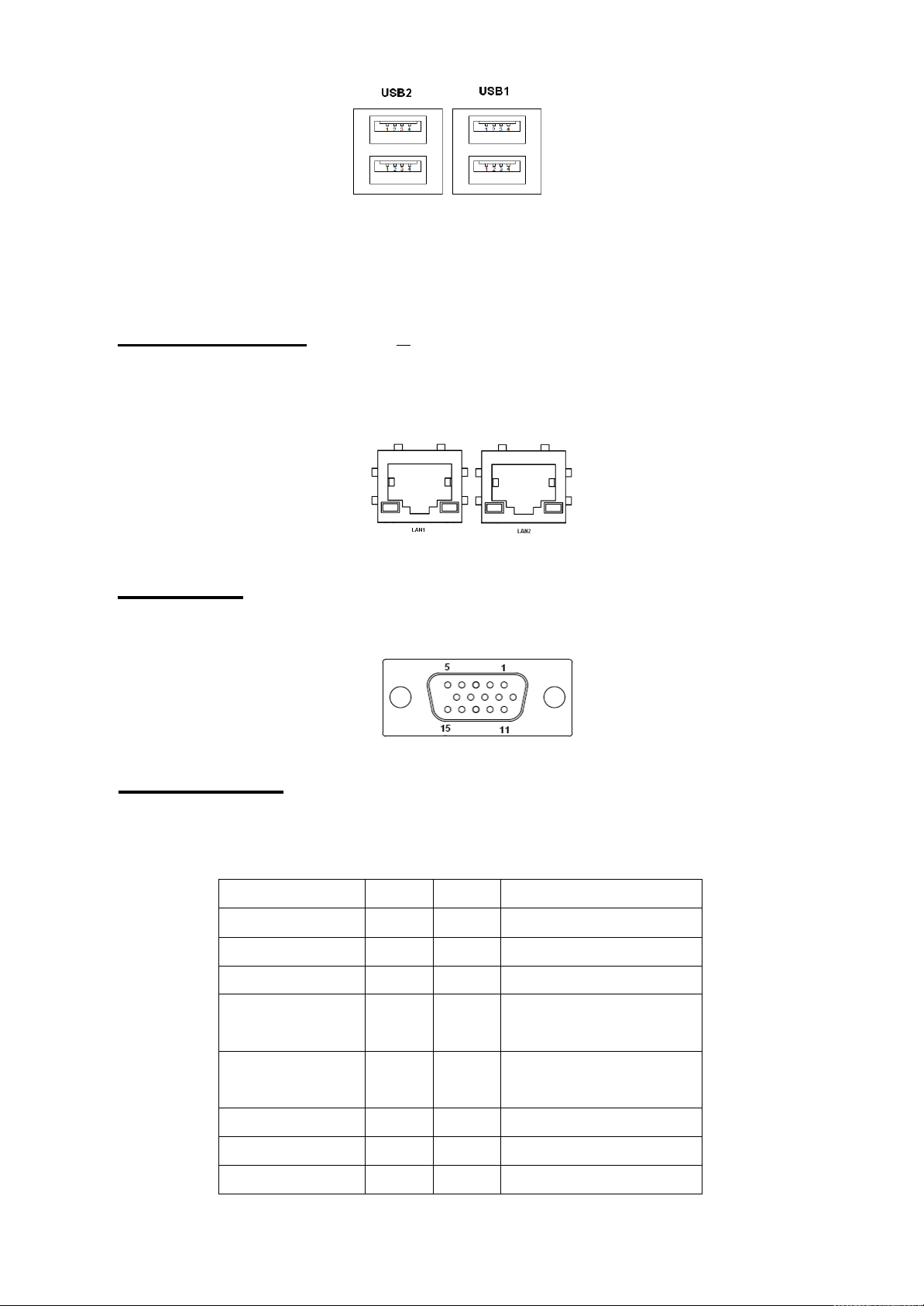
15. USB1/2: (Double stack USB type A), Rear USB connector, it provides up to 4
Page 21
Signal Name
Pin#
Pin#
Signal Name
CRT_RED
1
2
Ground
CRT_GREEN
3
4
Ground
CRT_BLUE
5
6
NC
CRT_R_HSYN
C
7
8
CRT_PU_DDC_DAT
CRT_R_VSYN
C
9
10
CRT_PU_DDC_CLK
NC
11
12
NC
+12V
13
14
Ground
+12V
15
16
Ground
USB2.0 ports, speed up to 480Mb/s.
Each USB Type A Receptacle (2 Ports) Current limited value is 1.5A.
If the external USB device current exceeds 1.5A, please separate connectors
into different Receptacle.
16. LAN1/2: (RJ45 Connector), Rear LAN port,2 standard 10/100/1000M RJ-45 Ethernet
ports are provided. Used Intel 82567LM chipset ,LINK LED (green) and ACTIVE LED
(yellow) respectively located at the left-hand and right-hand side of the Ethernet port
indicate the activity and transmission state of LAN.
17. VGA: (CRT Connector DB15),Video Graphic Array Port, provide high-quality video
output. They can not work at the same time for VGA and VGA-PH.
18. VGA-PH: (CRT 2.0mm Pitch 2x8 Pin Header), Video Graphic Array Port, Provide
2x8 Pin cable to VGA Port, they can not work at the same time for VGA and
VGA-PH.
Page 22
19. CPU SCREW HOLES: Four screw holes for fixed CPU Cooler assemble.
Pin#
Signal Name
1
+12V
2
Ground
Pin#
Signal Name
1
Ground
2
VCC
3
Rotation
detection
Signal Name
Pin#
Pin#
Signal Name
LVDS1_VDD5
1
2
LVDS1_VDD5
Ground
3
4
Ground
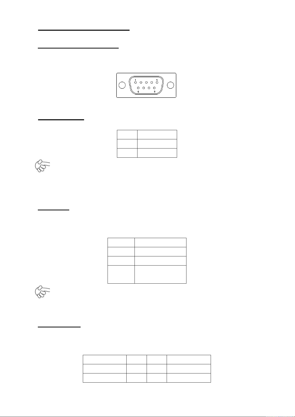
20. COM1: (Type DB9),Rear serial port, standard DB9 serial port is provided to make
a direct connection to serial devices. COM1 port is controlled by pins No.1~6 of JCOM,
select output Signal RI or 5V or 12v, For details, please refer to description of JCOM.
21. AT12V: (5.0mm 1x2 Pin Connector),DC12V System power input connector。
Note:
Make sure that the voltage of power supply is DC(12±5%)V before power on, or
it may cause boot up failure and even system damage.
22. FAN: (2.54mm Pitch 1x3 Pin Header), Fan connector, cooling fans can be
connected directly for use. You may set the rotation condition of cooling fan in menu of
BIOS CMOS Setup.
Note:
Output power of cooling fan must be limited under 5W.
23. LVDS: For 18 bit LVDS output connector, Fully supported by Intel Atom D525
chipset, the interface features single channel 18-bit output. Model name of the
interface connector is Hirose DF13-30DP-1.25V.
Page 23

LVDS1_VDD3
3
5
6
LVDS1_VDD3
3
LADATAN0
7
8
NC
LADATAP0
9
10
NC
LADATAN1
11
12
NC
LADATAP1
13
14
NC
LADATAN2
15
16
NC
LADATAP2
17
18
NC
LACLKN
19
20
NC
LACLKP
21
22
NC
LDDC_CLK
23
24
NC
LBKLT_EN
25
26
BKLT_CTRL
Ground
27
28
Ground
+V12S
29
30
+V12S
Pin#
Signal Name
1
+DC12V
2
+DC12V
3
Ground
4
Ground
5
BKLT_EN
6
BKLT_CTRL
Pin#
Signal
Name
1
+DC5V
2
Ground
3
Ground
4
+DC12V
24. BKL: (2.0mm Pitch 1x5 box Pin Header), Backlight control connector for LVDS1.
25. SATA1/2/3: (SATA 7P),SATA1,SATA2,SATA3 SATA Connectors. Three SATA
connectors are provided, with transfer speed up to 3.0Gb/s.
ASB-L706NE: SATA1/SATA2/SATA3 drives supporting RAID 0 or RAID 1 function
26. SATA_P2: (2.5mm Pitch 1x4 box Pin Header), onboard 5V and 12V output connector
is reserved to provide power for SATA devices.
Note:
Output current of the connector must not be above 1A.
Page 24

27. CN1: (2.5mm Pitch 1x2 box Pin Header), an onboard 5V output connector is
Pin#
Signal
Name
1
+DC5V
2
Ground
reserved to provide power for IDE/SATA devices.
Note:
Output current of the connector must not be above 1A.
28. PC104+: (4x30 Pin), PC104 plus connector, it conforms to standard PC104+
specification.
29. MPCIE2: (30mmx30mm Socket 52Pin), mini PCIE socket, it is located at the top, it
supports mini PCI-E devices with USB2.0, SMBUS and PCI-E signal.
30. MPCIE2 SCREW HOLES: one screw holes for fixed MPCIE2 assemble.
31. MPCIE: (50.95x30mm socket 52Pin), mini PCIE socket, it is located at the bottom,
it supports mini PCI-E devices with USB2.0, SMBUS and PCI-E signal.
32. CF: CF Card socket, it is located at the bottom of the board and serves as an insert
interface for Type I and Type II Compact Flash card. The operating voltage of CF card
can be set as 3.3V or 5V. The default setting of the product is 5V.
33. DDR3: (SO-DIMM 204Pin socket), DDRIII memory socket, the socket is located at the
bottom of the board and supports 204Pin 1.5V DDRIII 800MHz FSB SO-DIMM
memory module up to 2G.
34. MPCIE SCREW HOLES: one screw holes for fixed MPCIE assemble.
Page 25

Chapter 3 BIOS Setup
3.1 Operations after POST Screen
After CMOS discharge or BIOS flashing operation, the system will display the following screen for your
further operation. Press F2 key to continue or F1 key to enter CMOS Setup.
After optimizing and exiting CMOS Setup, the POST screen displayed for the first time is as follows
AMIBIOS© 2009 American Mega trends , Inc.
BIOS Date: 03/22/12 15:57:19 Ver: 08.00.16
CPU :
I
nte
l® Atom™ CPU D525 @ 1.80GHz
Speed : 1.80 GHz
Press F11 for BBS POPUP
Initializing USB Controllers. . Done.
2038MB OK
Auto-Detecting Pri Master.. IDE Hard Disk
Pri Master : Hitachi HTS545016B9A300 PB0C64G
Ultra DMA – 5, S.M.A.R.T. Capable and Status OK
Auto – detec ting USB Mass Storage Devices ..
00 USB Mass storage devices found and configured
CMOS Settings Wrong
CMOS Data / Time Not Set
Press F1 to Run SETUP
Press F2 to load default values and continue
0085
and includes basic information on BIOS, CPU, memory, and storage devices.
AMIBIOS© 2009 American Mega trends , Inc.
BIOS Date: 03/22/12 15:57:19 Ver: 08.00.16
CPU :
I
nte
l® Atom™ CPU D525 @ 1.80GHz
Speed : 1.80 GHz
Press DEL to Run Setup
Press F11 for BBS POPUP
Initializing USB Controllers. . Done.
2038MB OK
Auto-Detecting Pri Master.. IDE Hard Disk
Pri Master : Hitachi HTS545016B9A300 PB0C64G
Ultra DMA – 5, S.M.A.R.T. Capable and Status OK
Auto – detecting USB Mass Storage Devices ..
00 USB Mass storage devices found and configured.
Checking NVRAM..
0085
Press F11 key to enter Boot Menu during POST, as shown by the following figure.
Page 26

BIOS SETUP UTILITY
Main
Advanced
PCIPnP
Boot
Security
Chipset
Exit
System Overview
User [ENTER],[TAB]
or [SHIFT-TAB] to
Select a field
Use[+] or [-] to
configure system Time.
←
Select Screen
↑↓
Select Item
+- Charge Field
Tab Select Field
F1 General Help
F10 Save and Exit
AMIBIOS
Version : 08.00.16
Build Date : 03/22/12
ID : L706V012
Processor
Intel ® Atom™ CPU D525 @ 1.80GHz
Speed :1800MHz
Count :2
System Memory
Size :2038MB
System Time [00:00:10]
Please select boot device:
Hitachi HTS545016B9A300
USB: USB Hotplug FDD
↑
and ↓ to move selection
ENTER to select Boot device
ESC to boot using defaults
3.2 BIOS SETUP UTILITY
Press [Del] key to enter BIOS Setup utility during POST, and then a main menu containing system
summary information will appear.
Page 27

System Date [Tue
BIOS SETUP UTILITY
Main
Advanced
PCIPnP
Boot
Security
Chipset
Exit
System Overview
User [ENTER],[TAB]
or [SHIFT-TAB] to
Select a field
Use[+] or [-] to
configure system Time.
←
Select Screen
↑↓
Select Item
+- Charge Field
Tab Select Field
F1 General Help
F10 Save and Exit
ESC Exit
AMIBIOS
Version : 08.00.16
Build Date : 03/22/12
ID : L706V012
Processor
Intel ® Atom™ CPU D525 @ 1.80GHz
Speed :1800MHz
Count :2
System Memory
Size :2038MB
System Time [00:06:31]
System Date [Tue
01/01/2002]
V02.68
©
Copyright 1985-2009 American Mega trends , Inc.
ESC Exit
01/01/2002]
V02.68
3.3 System Overview
©
Copyright 1985-2009 American Mega trends , Inc.
System Time:
Set the system time, the time format is:
System Date:
Set the system date, the date format is:
Day: Note that the
Month: 01 to 12
Date: 01 to 31
Year: 2010 to 2099
Hour : 0 to 23
Minute : 0 to 59
Second : 0 to 59
„Day‟ automatically changes when you set the date.
Page 28

3.4 Advanced Settings
BIOS SETUP UTILITY
Main
Advanced
PCIPnP
Boot
Security
Chipset
Exit
Advanced Settings
Configure CPU
←
Select Screen
↑↓
Select Item
Enter Charge Field
F1 General Help
F10 Save and Exit
ESC Exit
WARNING: Setting wrong values In below
sections
may cause system to malfunction.
► CPU Configuration
► IDE Configuration
► Super IO Configuration
► Hardware Health Configuration
► ACPI Configuration
► AHCI Configuration
► ASF Configuration
► MPS Configuration
► PCI Express Configuration
► Smbios Configuration
► USB Configuration
V02.68
©
Copyright 1985-2009 American Mega trends , Inc.
BIOS SETUP UTILITY
Main
Advanced
PCIPnP
Boot
Security
Chipset
Exit
Advanced Settings
Configure CPU
←
Select Screen
↑↓
Select Item
Enter Charge Field
F1 General Help
F10 Save and Exit
WARNING: Setting wrong values In below
sections
may cause system to malfunction.
► CPU Configuration
► IDE Configuration
► Super IO Configuration
► Hardware Health Configuration
► ACPI Configuration
► AHCI Configuration
► ASF Configuration
► MPS Configuration
► PCI Express Configuration
3.4.1 CPU Configuration
Page 29

► Smbios Configuration
ESC Exit
► USB Configuration
V02.68
©
Copyright 1985-2009 American Mega trends , Inc.
BIOS SETUP UTILITY
Advanced
IDE Configuration
Options
Disabled
Enhanced
←
Select Screen
↑↓
Select Item
+- Charge Field F1
General Help F10
Save and Exit ESC
Exit
ATA/IDE Configuration [Enhanced]
Configure SATA as [IDE]
► Primary IDE Master : [Not
Detected]
► Primary IDE Slaver : [Not
Detected]
► Secondary IDE Master : [Not
Detected]
► Secondary IDE Slaver : [Not
Detected]
► Third IDE Master : [Not
Detected]
► Third IDE Slaver : [Not
Detected]
► Fourth IDE Master : [Not
Detected]
► Fourth IDE Slaver : [Not
Detected]
Hard Disk Write Protect [Disabled]
IDE Detect Time Out (Sec) [35]
ATA(PI) 80Pin Cable Detection [Host &
Device]
V02.68
©
Copyright 1985-2009 American Mega trends , Inc.
3.4.2 IDE Configuration
ATA/IDE Configuration:
Configure SATA as:
[Enhanced]
[Disabled]
Page 30

BIOS SETUP UTILITY
Advanced
Configure Win627UHG Super IO Chipset
Allow BIOS to Select
Serial Port Base
Address.
←
Select Screen
↑↓
Select Item
+- Charge Field F1
General Help F10
Save and Exit ESC
Exit
Serial Port1 Address [3F8]
Serial Port1 IRQ [IRQ4]
Serial Port2 Address [2F8]
Serial Port2 IRQ [IRQ3]
Serial Port3 Address [3E8]
Serial Port3 IRQ [IRQ5]
Serial Port3 Type [RS232
Type]
Serial Port4 Address [2E8]
Serial Port4 IRQ [IRQ6]
Serial Port5 Address [2F0]
Serial Port5 IRQ [IRQ10]
Serial Port6 Address [2E0]
Serial Port6 IRQ [IRQ11]
WatchDog Setting [Disable]
V02.68
©
Copyright 1985-2009 American Mega trends , Inc.
[IDE]
[RAID]
[AHCI]
Hard Disk Write Protect:
[Disabled]
[Enabled]
IDE Detect Time Out :
[35]
ATA(PI) 80Pin Cable Detection:
3.4.3 Super IO Configuration
Options: [0,5,10,15,20,25,30,35]
[Host & Device]
[Host]
[Device]
Serial Port3 Type:
COM3 Options:
[RS232 Type]
Page 31

BIOS SETUP UTILITY
Advanced
Hardware Health Configuration
Fan configuration mode
setting
←
Select Screen
↑↓
Select Item
+- Charge Field F1
General Help F10
Save and Exit ESC
Exit
CPU Temperature :41℃/105℉
CPUFAN Speed :4800 RPM
CPUFAN Mode Setting [Manual
Mode ]
CPUFAN PWM Control [250 ]
V02.68
©
Copyright 1985-2009 American Mega trends , Inc.
[RS485 Type]
WatchDog Setting:
Options: [10sec,20sec,30sec,40sec,1min,2min,4min]
3.4.4 Hardware Health Configuration
[Disable]
3.4.5 ACPI Configuration
3.4.6 AHCI Configuration
CPU Temperature:
Show you the current CPU temperature.
CPUFAN Speed:
Show you the current CPU Fan operating speed.
CPUFAN Mode Setting:
Section for Advanced ACPI Configuration
Options:
[Manual Mode]
[Thermal Cruise Mode]
[Speed Cruise Mode]
[Smart Fan3 Mode]
[Advanced ACPI Configuration]
[Chipset ACPI Configuration]
Page 32

BIOS SETUP UTILITY
Advanced
AHCI Configuration
While entering setup,
BIOS auto detects the
presence of IDE
devices. This displays
the status of auto
detecting of IDE
devices
←
Select Screen
↑↓
Select Item
Enter Go to sub screen
F1 General Help
F10 Save and Exit
ESC Exit
► AHCI Port0 : [Not
Detected]
► AHCI Port1 : [Not
Detected]
► AHCI Port2 : [Not
Detected]
V02.68
©
Copyright 1985-2009 American Mega trends , Inc.
BIOS SETUP UTILITY
Advanced
MPS Configuration
Select
Revision
←
Select Screen
↑↓
Select Item
+- Charge Field F1
General Help F10
Save and Exit
ESC Exit
MPS Revision [1.4]
V02.68
©
Copyright 1985-2009 American Mega trends , Inc.
While entering setup, BIOS auto detects the presence of IDE devices. This displays the
status of auto detecting of IDE devices
3.4.7 MPS Configuration
Configure the Multi-Processor Table.
MPS Revision:
Page 33

[1.4]
Page 34

BIOS SETUP UTILITY
Advanced
PCI Express Configuration
Enables/Disables
PCI Express Device
Relaxed Ordering
←
Select Screen
↑↓
Select Item
+- Charge Field
F1 General Help
F10 Save and Exit
ESC Exit
Relaxed Ordering [Auto]
Maximum Payload Size [Auto]
Extended Tag Field [Auto]
No Snoop [Auto]
Maximum Read Request Size [Auto]
Active State Power Management [Disabled]
Extended Synch [Auto]
V02.68
©
Copyright 1985-2009 American Mega trends , Inc.
3.4.8 PCI Express Configuration
[1.1]
Relaxed Ordering:
Maximum Payload Size:
[Auto]
[Disabled]
[Enable]
[Auto]
[128/256/512/1024/2048/4096 Bytes]
Set Maximum Payload of allow System BIOS select the value.
Extended Tag Field:
[Auto]
[Disabled]
[Enable]
No Snoop:
[Auto]
Maximum Read Request Size:
[Auto]
[128/256/512/1024/2048/4096 Bytes]
Set Maximum Read Request Size of PCI Express Device or allow
System BIOS select the value.
[Disabled]
[Enable]
Page 35

Active State Power Management:
BIOS SETUP UTILITY
Advanced
Smbios Configuration
SMBIOS SMI Wrapper
Support for PnP Func
50h-54h
←
Select Screen
↑↓
Select Item
+- Charge Field
F1 General Help
F10 Save and Exit
ESC Exit
Smbios Smi Support [Enabled]
V02.68
©
Copyright 1985-2009 American Mega trends , Inc.
BIOS SETUP UTILITY
Advanced
[Disabled]
Extended Synch:
3.4.9 Smbios Configuration
[Enable]
[Auto]
[Disabled]
[Enable]
Smbios Smi Support:
3.4.10 USB Configuration
[Enable]
[Disabled]
Page 36

USB Configuration
Enables support for
legacy USB.ATUO
option disables legacy
support if no USB
devices are connected
←
Select Screen
↑↓
Select Item
+- Charge Field
F1 General Help
F10 Save and Exit
ESC Exit
Module Version – 2.24.5-14.4
USB Devices Enabled :
None
Legacy USB Support [Enabled]
USB2.0 Controller Mode
[Hispeed]
BIOS EHCI Hand-Off [Enabled]
Hotplug USB FDD Support [Auto]
► USB Mass Storage Device Configuration
V02.68
©
Copyright 1985-2009 American Mega trends , Inc.
Legacy USB Support:
[Enable]
USB2.0 Controller Mode:
BIOS EHCI Hand-Off:
Hotplug USB FDD Support:
USB Mass Storage Device Configuration:
[Disabled]
[HiSpeed]
[FullSpeed]
[Enable]
[Disabled]
[Auto]
[Disabled]
[Enable]
BIOS SETUP UTILITY
Page 37

Advanced
USB Mass Storage Device Configuration
Number of seconds
POST waits for the USB
mass storage device
after start unit command
←
Select Screen
↑↓
Select Item
+- Charge Field F1
General Help F10
Save and Exit ESC
Exit
USB Mass Storage Reset Delay [20 Sec]
Device #1 USB Hotplug
Emulation Type [Auto]
V02.68
©
Copyright 1985-2009 American Mega trends , Inc.
BIOS SETUP UTILITY
Main
Advanced
PCIPNP
Boot
Security
Chipset
Exit
Advanced PCI/PnP Settings
Clear NURAM during
System Boot
←
Select Screen
↑↓
Select Item
+- Charge Field
F1 General Help
WARNING: Setting wrong values In below
sections
may cause system to malfunction.
Clear NVRAM [No]
Plug & Play O/S [No]
PCI Latency Timer [64]
Allocate IRQ to PCI VGA [Yes]
Palette Snooping [Disabled]
PCI IDE BusMaster [Enabled]
OffBoard PCI/ISA IDE Card [Auto]
IRQ3
[Available]
3.5 Advanced PCI/PnP Settings
This part describes configurations to be made on PCI bus system. PCI, namely Personal Computer
Interconnect, is a computer bus that allows I/O device to operate nearly as fast as CPU in its own way.
Some technical terms will be mentioned here. We recommend that non-professional users not
make changes from factory default settings.
Page 38

IRQ4
[Available]
F10 Save and Exit
ESC Exit
IRQ5
[Available]
IRQ6
[Available]
IRQ7
[Available]
IRQ9
[Available]
IRQ10
[Available]
V02.68
©
Copyright 1985-2009 American Mega trends , Inc.
Clear NVRAM:
[Yes]
[No]
Plug & Play OS:
[No]
[Yes]
PCI Latency Timer:
[32]
[96]
[128]
[160]
[192]
[224]
[248]
[64]
Allocate IRQ to PCI/VGA:
[
No]
Palette Snooping:
[Yes]
[Disabled]
[Enable]
PCI IDE BusMaster:
[Disabled]
Page 39

[Enable]
OffBoard PCI/ISA IDE Card:
Some PCI IDE cards may require this to be set to the PCI slot number that is
holding the card. Auto:Works for most PCI IDE Cards.
[Auto]
[PCI Slot1]
[PCI Slot2]
[PCI Slot3]
[PCI Slot4]
[PCI Slot5]
[PCI Slot6]
IRQ3/4/5/7/9/10/11/14/15:
[Available]
[
Reserved]
Available: Specified IRQ is available to be used by PCI/PnP devices.
Reserved: Specified IRQ is reserved for use by legacy ISA devices.
DMA Channel 0/1/3/5/6/7:
[Available]
[
Reserved]
Available: Specified DMA is available to be used by PCI/PnP devices.
Reserved: Specified DMA is reserved for use by legacy ISA devices.
Reserved Memory Size:
Size of memory block to reserve for legacy ISA devices.
[Disabled]
[16k]
[32k]
[64k]
Page 40

3.6 Boot Settings
BIOS SETUP UTILITY
Main
Advanced
PCIPnP
Boot
Security
Chipset
Exit
Boot Settings
Configure Settings
During System Boot
←
Select Screen
↑↓
Select Item
+- Charge Field F1
General Help F10
Save and Exit
ESC Exit
► Boot Setting Configuration
► Boot Device Priority
V02.68
©
Copyright 1985-2009 American Mega trends , Inc.
Boot Setting Configuration:
Quick Boot:
Allows BIOS to skip certain tests while booting .This will decrease the time
needed to boot the system.
Quiet Boot:
Disabled: Displays normal POST messages.
Enabled: Displays OEM logo instead of POST messages.
AddOn ROM Display Mode:
Set display mode for Option ROM.
[Enabled]
[Disabled]
[Disabled]
[Enabled]
Page 41

[Force BIOS]
[Keep Current]
Bootup Num-Lock:
Select Power-on state for Numlock.
[On]
[Off]
PS/2 Mouse Support,:
Select support for PS/2 Mouse.
[Auto]
[Enabled]
[Disabled]
Wait For „F1‟ If Error:
Wait for F1 key to be pressed if error occurs.
[Enabled]
[Disabled]
Hit „DEL‟Messgae Display :
Interrupt 19 Capture:
Boot Device Priority:
Specifies the Boot Device Priority sequence.
Displays “press” DEL to run Setup in POST.
[Enabled]
[Disabled]
[Disabled]
[Enabled]
Enabled: Allows option ROMs to trap interrupt 19.
Page 42

3.7 Security Settings
BIOS SETUP UTILITY
Main
Advanced
PCIPnP
Boot
Security
Chipset
Exit
Security Settings
Install or Change the
password.
←
Select Screen
↑↓
Select Item
Enter Charge
F1 General Help
F10 Save and Exit
ESC Exit
Supervisor Password :Not Installed
User Password :Not Installed
Change Supervisor Password
Change User Password
Boot Sector Virus Protection [Disabled]
V02.68
©
Copyright 1985-2009 American Mega trends , Inc.
Change Supervisor Password:
Install or Change the password.
Change User Password:
Install or Change the password.
Password Check:
[Setup]
[Always]
Setup: Check password while invoking setup.
Always: Check password while invoking setup a well as on each boot.
Boot Sector Virus Protection:
[Disabled]
[Enabled]
Enabled / Disabled Boot Sector Virus Protection.
Type the password with up to 6 characters and then press Enter key. This will
clear all previously typed CMOS passwords. You will be requested to confirm the
Page 43

password. Type the password again and press Enter key. You may press Esc
BIOS SETUP UTILITY
Main
Advanced
PCIPnP
Boot
Security
Chipset
Exit
Advanced Chipset Settings
Configure North Bridge
feature
←
Select Screen
↑↓
Select Item
Enter Go to sub screen
F1 General Help
F10 Save and Exit
ESC Exit
WARNING: Setting wrong values in below
sections
may cause system to malfunction
► North Bridge Configuration
► South Bridge Configuration
V02.68
©
Copyright 1985-2009 American Mega trends , Inc.
key to abandon password entry operation.
To clear the password, just press Enter key when password input window pops up.
A confirmation message will be shown on the screen as to whether the password will
be disabled. You will have direct access to BIOS setup without typing any password
after system reboot once the password is disabled.
Once the password feature is used, you will be requested to type the password each
time you enter BIOS setup. This will prevent unauthorized persons from changing
your system configurations.
Also, the feature is capable of requesting users to enter the password prior to system
boot to control unauthorized access to your computer. Users may enable the feature
in Security Option of Advanced BIOS Features. If Security Option is set to System,
you will be requested to enter the password before system boot and when entering
BIOS setup; if Security Option is set to Setup, you will be requested for password for
entering BIOS setup.
3.8 Advanced Chipset Settings
Note: Due to limited address length of BIOS, only a portion of panel parameters are listed in
Page 44

BIOS Setup. If the connected panel is not included in the parameter list, display
BIOS SETUP UTILITY
Chipset
North Bridge Chipset Configuration
Options
Auto
Max MHz
←
Select Screen
↑↓
Select Item
+- Charge Field
F1 General Help
F10 Save and Exit
ESC Exit
PCI MMIO Allocation: 4Gb To 3072MB
DRAM Frequency [Auto]
Configure DRAM Timing by SPD [Enabled]
Initate Graphic Adapter [IGD]
Internal Graphics Mode Select
[Enable,8MB]
PEG Port Configuration
► Video Function Configuration
V02.68
©
Copyright 1985-2009 American Mega trends , Inc.
problem will occur. In this case, Please do not change BIOS setup.
3.8.1 North Bridge Configuration
DRAM Frequency:
Configure DRAM Timing By SPD:
Initate Graphic Adapter:
Select which graphics controller to use as the primary boot device.
[Auto]
[Max MHz]
[Enabled]
[Disabled]
[IGD]
[PCI/IGD]
[PCI/PEG]
[PEG/IGD]
Page 45

[PCIE/PCI]
BIOS SETUP UTILITY
Chipset
Video Function Configuration
Options
Fixed Mode
DVMT Mode
←
Select Screen
↑↓
Select Item
+- Charge option
F1 General Help
F10 Save and Exit
ESC Exit
DVMT Mode Select [DVMT
Mode]
DVMT/FIXED Memory
[256MB]
Boot Display Device
[VBIOS-Default]
Flat Panel Type
[1024x768LVDS]
Panel Backlight Control [Level 9]
HDCP Support
Disabled]
V02.68
©
Copyright 1985-2009 American Mega trends , Inc.
Internal Graphics Mode Select:
Video Function Configuration:
[Enabled, 8MB]
DVMT Mode Select:
[DVMT Mode]
[FIXED Mode]
Page 46

DVMT/FIXED Memory Size:
BIOS SETUP UTILITY
Chipset
North Bridge Chipset Configuration
Options
Auto
Max MHz
←
Select Screen
↑↓
Select Item
+- Charge Field
F1 General Help
PCI MMIO Allocation: 4Gb To 3072MB
DRAM Frequency [Auto]
Configure DRAM Timing by SPD [Enabled]
Initate Graphic Adapter [IGD]
Internal Graphics Mode Select
[Enable,8MB]
PEG Port Configuration
[256MB]
[128MB]
[Maximum DVMT]
Boot Display Device:
[VBIOS-Default]
[CRT]
[LVDS]
[CRT + LVDS]
Flat Panel Type:
Panel Backlight Control:
[1024x 768LVDS]
[640x480LVDS]
[800x600LVDS]
[1280x1024LVDS]
[1366x768LVDS]
[Level9]
[Level0~15]
Note: Panel support PWM Function.
3.8.2 South Bridge Configuration :
Page 47

F10 Save and Exit
ESC Exit
► Video Function Configuration
V02.68
©
Copyright 1985-2009 American Mega trends , Inc.
BIOS SETUP UTILITY
Chipset
Video Function Configuration
Options
Fixed Mode
DVMT Mode
DVMT Mode Select [DVMT
Mode]
DRAM Frequency:
[Auto]
[Max MHz]
Configure DRAM Timing By SPD:
[Enabled]
[Disabled]
Initate Graphic Adapter:
Select which graphics controller to use as the primary boot device.
[IGD]
[PCI/IGD]
[PCI/PEG]
[PEG/IGD]
[PCIE/PCI]
Internal Graphics Mode Select:
Video Function Configuration:
[Enabled, 8MB]
Page 48

DVMT/FIXED Memory
[256MB]
←
Select Screen
↑↓
Select Item
+- Charge option
F1 General Help
F10 Save and Exit
ESC Exit
Boot Display Device
[VBIOS-Default]
Flat Panel Type
[1024x768LVDS]
Panel Backlight Control [Level 9]
HDCP Support
Disabled]
V02.68
©
Copyright 1985-2009 American Mega trends , Inc.
DVMT Mode Select:
[DVMT Mode]
[FIXED Mode]
DVMT/FIXED Memory Size:
[256MB]
[128MB]
[Maximum DVMT]
Boot Display Device:
[VBIOS-Default]
[CRT]
[LVDS]
[CRT + LVDS]
Flat Panel Type:
[1024x 768LVDS]
[640x480LVDS]
[800x600LVDS]
[1280x1024LVDS]
[1366x768LVDS]
Page 49

Panel Backlight Control:
BIOS SETUP UTILITY
Main
Advanced
PCIPnP
Boot
Security
Chipset
Exit
Exit Options
Exit system setup
after saving the
changes
F10 key can be used
For this operation
←
Select Screen
↑↓
Select Item
Enter Go to sub screen
F1 General Help
F10 Save and Exit
ESC Exit
Save Changes and Exit
Discard Changes and Exit
Discard Changes
Load Optimal Defaults
Load Failsafe Defaults
V02.68
©
Copyright 1985-2009 American Mega trends , Inc.
[Level9]
[Level0~15]
Note: Panel support PWM Function.
3.9 Exit Options
Save Changes and Exit:
Save configuration changes and exit setup?
(F10 key can be used for this operation)
Discard Changes and Exit:
Discard Changes and Exit setup?
(ESC key can be used for this operation)
[OK]
[Cancel]
[OK]
Page 50

[Cancel]
Discard Changes:
Diacard changes?
(F7 key can be used for this operation)
[OK]
Load Optimized Defaults:
Load Optimized Defaults?
(F9 key can be used for this operation)
Load Fail-Safe Defaults:
Load Fail-Safe Defaults?
(F9 key can be used for this operation)
3.10 Examples of GPIO Programming
3.10.1 SuperIO Model: Winbond W83627UHG
[Cancel]
[OK]
[Cancel]
[OK]
[Cancel]
GPIO OUT use GP 60~63
GPIO IN use GP 20~23
3.10.2 W83627UHG Access index port: 4Eh/4Fh
Index Address Port: 4Eh
Index Data Port: 4Fh
3.10.3 Configure GPIO register sequence
1. Enter the extended function mode
2. Select logic device number 8
3. Activate the logic device GPIO Port 6
4. Configure GPIO Port 6 register
5. Select logic device number 9
6. Activate the logic device GPIO Port 2
7. Configure GPIO Port 2 register
8. Exit the extended function mode
Page 51

outportb(0x4E, 0x07); //LDN selection register
3.10.4 Read/write GPIO sequence
1. Enter the extended function mode
2. Select logic device number
3. Read/write GPIO register value
4. Exit the extended function mode
3.10.5 Software programming example
Enter the extended function mode
Writing 87h to index address port twice will enter the extended function mode.
Example x86 assembly code:
mov dx, 4Eh
mov al, 87h
out dx, al
out dx, al
Example C code:
outportb(0x4E, 0x87);
outportb(0x4E, 0x87);
Exit the extended function mode
Writing AAh to index address port will exit the extended function mode.
Example x86 assembly code:
mov dx, 4Eh
mov al, 0AAh
out dx, al
Example C code:
outportb(0x4E, 0xAA);
Select logic device number
Example x86 assembly code:
mov dx, 4Eh
mov al, 007h ;LDN selection register
out dx, al
mov dx, 4Fh
mov al, 008h ;Select LDN=8, GPIO Port6
;or Select LDN9, GPIO Port2
out dx, al
Example C code:
Page 52

outportb(0x4F, 0x08); //Select LDN=8, GPIO Port6
or
outportb(0x4E, 0x07); //LDN selection register
outportb(0x4F, 0x09); //Select LDN=9, GPIO Port2
Activate the logic device
Example x86 assembly code:
mov dx, 4Eh
mov al, 030h ;Logic device activation control reg.
out dx, al
mov dx, 4Fh
in al, dx
or al, 004h ;Set bit2 to enable GPIO Port6 if LDN=8
or al, 002h ;Set bit1 to enable GPIO Port2 if LDN=9
out dx, al
Example C code:
outportb(0x4E, 0x30); //Logic device activation control
outportb(0x4F, (inportb(0x4F)|0x2));
//Set bit[1] to enable GPIO Port2 if LDN=9
Or
outportb(0x4E, 0x30); //Logic device activation control
outportb(0x4F, (inportb(0x4F)|0x4));
//Set bit[2] to enable GPIO Port6 if LDN=8
Configure GPIO register
Example x86 assembly code:
mov dx, 4Eh
mov al, 0E6h ;GPIO inversion reg.
out dx, al
mov dx, 4Fh
mov al, 000h ;0 – normal, 1 - inverted
out dx, al
mov dx, 4Eh
mov al, 0E4h ;GPIO I/O selection reg.
out dx, al
mov dx, 4Fh
mov al, 0FFh ;0 – Output, 1 – Input
;or mov al, 0F0h to set output
Page 53

out dx, al
Example C code:
outportb(0x4E, 0xE6); //GPIO I/O selection reg.
outportb(0x4F, 0x0); //0 – normal, 1 – inverted
outportb(0x4E, 0xE4); //GPIO inversion reg.
outportb(0x4F, 0xFF); //0 – Output, 1 - Input
or
outportb(0x4E, 0xE4); //GPIO inversion reg.
outportb(0x4F, 0xF0); //0 – Output, 1 – Input
Read GPIO value
Example x86 assembly code:
mov dx, 4Eh
mov al, 0E5h ;GPIO data reg.
out dx, al
mov dx, 4Fh
in al, dx ;Bit[3::0] = GPI[3::0] value
Example C code:
outportb(0x4E, 0xE5); //GPIO data reg.
GP = inportb(0x4F); //Bit[3::0] = GPI[3::0]
Write GPIO value
Example x86 assembly code:
;Set GPO62
mov dx, 4Eh
mov al, 0E5h ;GPIO data reg.
out dx, al
mov dx, 4Fh
in al, dx
or al, 00000100b ;Bit2 = GPO62
out dx, al
;Clear GPO62
mov dx, 4Eh
mov al, 0E5h ;GPIO data reg.
out dx, al
mov dx, 4Fh
in al, dx
and al, not 00000100b
Page 54

Example C code:
//Set GPO62
outportb(0x4E, 0xE5); //GPIO data reg.
Outportb(0x4F, (inportb(0x4F)|0x4)); //Set Bit[2]
//Clear GPO62
outportb(0x4E, 0xE5); //GPIO data reg.
Outportb(0x4F, (inportb(0x4F)&0xFB)); //Clear Bit[2]
The followings are C language source code:
#include "stdio.h"
#include "conio.h"
//Super I/O index access port
#define INDEXP 0x4E
#define DATAP 0x4F
//Enter super I/O programming mode
#define ENTERPRG { \
outportb(INDEXP, 0x87); \
outportb(INDEXP, 0x87);}
//Super I/O index write
#define WRITEREG(reg,val) { \
outportb(INDEXP, reg); \
outportb(DATAP, val);}
//Exit super I/O programming mode
#define EXITPRG { \
outportb(INDEXP, 0xAA);}
//Select logic device number
#define SELETDEV(ldn) { \
outportb(INDEXP, 7); \
outportb(DATAP, ldn); }
//Initialize the GPIO port2
int InitGP2() {
//Start the super I/O chip programming
Page 55

ENTERPRG
//Select the logical device 9, GP2
SELETDEV(9)
//Activate GP1
WRITEREG(0x30, (inportb(0x30)|0x2))
WRITEREG(0xE6, 0x0)
WRITEREG(0xE4, 0xFF)
//Exit the super I/O chip programming
EXITPRG
return 0;
}
//Initialize the GPIO port6
int InitGP6() {
//Start the super I/O chip programming
ENTERPRG
//Select the logical device 8, GP6
SELETDEV(8)
//Activate GP1
WRITEREG(0x30, (inportb(0x30)|0x4))
WRITEREG(0xE6, 0x0)
WRITEREG(0xE4, 0xF0)
//Exit the super I/O chip programming
EXITPRG
return 0;
}
//Read GPIO Port2
unsigned char ReadGP2() {
unsigned char cGP2;
Page 56

//Start the super I/O chip programming
ENTERPRG
//Select the logical device 9, GP2
SELETDEV(9)
//Read GPIO Value
outportb(INDEXP, 0xE5);
cGP2 = inportb(DATAP);
cGP2 = cGP2 & 0xF;
//Exit the super I/O chip programming
EXITPRG
return cGP2;
}
//Write GPIO Port6
int WriteGP6(unsigned char cGP6) {
//Start the super I/O chip programming
ENTERPRG
//Select the logical device 8, GP6
SELETDEV(8)
//Write GP1 value
WRITEREG(0xE5, cGP6)
//Exit the super I/O chip programming
EXITPRG
return 0;
}
int main() {
unsigned char cGP;
//Initialize the GPIO port
InitGP2();
Page 57

InitGP6();
//Read GPIO Port 2
cGP = ReadGP2();
printf("\nRead GPIO Port 2 Status: %X", cGP);
//Write GPIO Port 6
WriteGP6(cGP);
printf("\nSet GPIO Port 6 Status: %X", cGP);
return 0;
Page 58

Chapter 4 Installation of Drivers
This chapter describes the installation procedures for software and drivers under the windows XP. The
software and drivers are included with the motherboard. The contents include Chipset Atom D525 +
ICH8M, GMA 3150 VGA Chipset, Network Adapter, Realtek ALC662 HD Audio Driver, Touch
Panel Driver.
Installation instructions are given below.
Important Note:
After installing your Windows operating system (Windows XP), you must install
first the Intel Chipset Software Installation Utility before proceeding with the
installation of drivers.
I
Page 59

4.1 Chipset Driver
To install the chipset driver, please follow the steps below.
Step 1. Access Industrial Panel PC. Select Chipset Atom D525 + ICH8M.
Step 2. Click Next to setup program.
Page 60

Step 3. Read the license agreement. Click Yes to accept the terms of the license agreement.
Step 4. Click Next to continue.
Page 61

Step 5. Click Next.
Step 6. Select Yes, I want to restart this computer now. Click Finish then remove any installation
media from the drives.
Page 62

4.2 GMA 3150 VGA Chipset Driver
To install the VGA drivers, follow the steps below to proceed with the installation.
Step 1. Select GMA 3150 VGA Chipset.
Step 2. Click Next to continue.
Page 63

Step 3. Click Next to continue setup program.
Step 4. Read the license agreement. Click Yes to accept the license agreement.
Page 64

Step 5. Click Next.
Step 6. Click Next to continue.
Page 65

Step 7. Select Yes, I want to restart this computer now. Click Finish then remove any installation
media from the drivers.
Page 66

4.3 Network Adapter Driver
To install the Network adapter Driver, please follow the steps below.
Step 1. Select Network Adapter.
Step 2. Click Next to continue.
Page 67

Step 3. Read license agreement. Select I accept the terms in the license agreement then click
Next to continue.
Step 4. Select Drivers, PROSet for Windows* Device Manager, Advanced Network
Services. Click Next to continue.
Page 68

Step 5. Click Install to begin the installation.
Step 6. Click Finish to compete the installation.
Page 69

4.4 Realtek HD Audio Driver Installation
To install the Realtek High Definition (HD) Audio driver, please follow the steps below.
Step 1. Select Realtek ALC662 HD Audio Driver from the list.
Step 2. Wait for extracting the files then click Next to continue.
Page 70

Step 3. Click Yes to continue the installation.
Step 4. Wait for installation.
Page 71

Step 5. Select Yes, I want to restart my computer now. then click OK.
Page 72

Chapter 5 Touch Screen Installation
This chapter describes how to install drivers and other software that will allow your PenMount 6000
Controller Board to work with different operating systems.
NOTE: PenMount USB drivers support up to 15 USB controllers.
5.1 Introduction to Touch Screen Controller Board
PenMount 6300 USB control board is a touch screen control board designed for USB interface and
specific for 4, 5, 8-wire touch screens. It is designed with USB interface features with multiple devices
supporting function. PenMount 6300 control board using PenMount 6000 controller that has been
designed for those who may like and all-in-one solution with 10-bit A/D converter built-in to make the
total printed circuit board denser, circuit diagram also designed for 12-bit ADC for optional. There are
two connectors on this board, one connector is for 4, 5, 8-wire touch screen cable (optional), and
another is for 4-pin USB A type cable (optional).
Figure 5.1: Bird‟s Eye View of Control Board
5.2 Windows 2000/XP/2003/Vista Universal Driver Installation
for PenMount 6000 Series
Before installing the Windows 2000/XP driver software, you must have the Windows 2000/XP system
installed and running on your computer. You must also have one of the following PenMount 6000
series controller or control boards installed: PM6500, PM6300.
5.2.1 Installing Software
If you have an older version of the PenMount Windows 2000/XP driver installed in your system, please
remove it first. Follow the steps below to install the PenMount DMC6000 Windows 2000/XP driver.
Page 73

Step 1. Please make sure your PenMount 6000 device had plugged in advance. If your device uses
RS232 interface, please plugged in before the machine is turned on. When the system first detects the
controller board, a screen appears that shows “Unknown Device”. Do not use this hardware wizard.
Press Cancel.
Step 2. Insert the product CD install setup.exe. the screen below would appear. Se touch panel driver
Step 3. Click Next to continue.
Page 74

Step 4. Read the license Agreement. Click I agree to agree the license agreement.
Step 5. Choose the folder in which to install PenMount Windows Universal Driver. Click Install to
start the installation.
Page 75

Step 6. Wait for installation. Then click Next to continue.
Step 7. Click OK.
Page 76

Step 8. Click Finish to compete installation.
Page 77

5.2.2 Software Functions
Upon rebooting, the computer automatically finds the new 6000 controller board. The touch screen is
connected but not calibrated. Follow the procedures below to carry out calibration.
1. After installation, click the PenMount Monitor icon “PM” in the menu bar.
2. When the PenMount Control Panel appears, select a device to “Calibrate.”
PenMount Control Panel
The functions of the PenMount Control Panel are Device, Multiple Monitors, Tools and About,
which are explained in the following sections.
Device
In this window, you can find out that how many devices are detected on your system.
Calibrate
This function offers two ways to calibrate your touch screen. „Standard Calibration‟ adjusts most touch
screens. „Advanced Calibration
‟
adjusts aging touch screens.
Standard Calibration Click this button and arrows appear
pointing to red squares. Use your finger or
stylus to touch the red squares in
sequence. After the fifth red point
calibration is complete. To skip, press
„ESC‟.
Page 78

Advanced Calibration
Advanced Calibration uses 4, 9, 16 or 25
points to effectively calibrate touch panel
linearity of aged touch screens. Click this
button and touch the red squares in
sequence with a stylus. To skip, press
ESC‟.
Command Calibration
Command call calibration function. Use
command mode call calibration function,
this can uses Standard, 4, 9, 16 or 25
points to calibrate E.g. Please run ms-dos
prompt or command prompt c:\Program
Files\PenMount Universa Driver\Dmcctrl.exe
-calibration 0 ( Standard Calibration)
Dmcctrl.exe - calibration ($) 0= Standard
Calibration 4=Advanced Calibration 4
9=Advanced Calibration 9 16=Advanced
Calibration 16 25=Advanced Calibration 25
Step 1. Please select a device then click Configure. You can also double click the device too.
Page 79

Step 2. Click Standard Calibration to start calibration procedure
NOTE: The older the touch screen, the more Advanced Mode calibration points you need for an
accurate calibration. Use a stylus during Advanced Calibration for greater accuracy. Please follow the
step as below:
Page 80

Step 3. Come back to PenMount Control Panel and select Tools then Click Advanced
Calibration.
Step 4. Select Device to calibrate, then you can start to do “Advanced Calibration”.
NOTE: Recommend to use a stylus during Advanced Calibration for greater accuracy.
Page 81

Setting
Page 82

About
This panel displays information about the PenMount controller and driver version.
Page 83

Multiple Monitors
Multiple Monitors supports from two to six touch screen displays for one system. The PenMount
drivers for Windows 2000/XP support Multiple Monitors. This function supports from two to six touch
screen displays for one system. Each monitor requires its own PenMount touch screen control board,
either installed inside the display or in a central unit. The PenMount control boards must be connected
to the computer COM ports via the RS-232 interface. Driver installation procedures are the same as
for a single monitor. Multiple Monitors supports the following modes:
Windows Extend Monitor Function
Matrox DualHead Multi-Screen Function
nVidia nView Function
NOTE: The Multiple Monitors function is for use with multiple displays only. Do not use this function if
you have only one touch screen display. Please note once you turn on this function the Rotating
function is disabled.
Enable the multiple display function as follows:
Step 1. Check the Multiple Monitor Support box; then click Map Touch Screens to assign touch
controllers to displays.
Page 84

Step 2. When the mapping screen message appears, click OK.
Step 3. Touch each screen as it displays Please touch this monitor. Press
sequence and touching each screen is called mapping the touch screens.
„S‟
to skip Following this
Step 4. After the setting procedure is finished, maybe you need to calibrate for each panel and
controller
NOTES:
1. If you used a single VGA output for multiple monitors, please do not use the Multiple Monitors
function. Just follow the regular procedure for calibration on each of your desktop monitors.
2. The Rotating function is disabled if you use the Multiple Monitors function.
3. If you change the resolution of display or screen address, you have to redo Map Touch Screens so
Page 85

the system understands where the displays are.
Draw
Tests or demonstrates the PenMount touch
screen operation.
Advanced Calibration
Enable Advanced Calibration function
Right Button Icon
Enable right button function. The icon can
show on Desktop or System Tray (menu bar).
4. If you more monitor mapping one touch screen, Please press
Tools
„S‟
to skip mapping step.
Page 86

About
You can see how many devices of PenMount controller that are plugged to your system
PenMount Monitor Menu Icon
The PenMount monitor icon (PM) appears in the menu bar of Windows 2000/XP system when you
turn on PenMount Monitor in PenMount Utilities.
PenMount Monitor has the following function
Page 87

PenMount Rotating Functions
The PenMount driver for Windows 2000/XP supports several display rotating software packages.
Windows Me/2000/XP support display rotating software packages such as:
• Portrait‟s Pivot Screen Rotation Software
• ATI Display Driver Rotate Function
• nVidia Display Driver Rotate Function
• SMI Display Driver Rotate Function
• Intel 845G/GE Display Driver Rotate Function
Configuring the Rotate Function
1. Install the rotation software package.
2. Choose the rotate function (0°, 90°, 180°, 270°) in the 3rd party software. The calibration screen
appears automatically. Touch this point and rotation is mapped.
NOTE: The Rotate function is disabled if you use Monitor Mapping
 Loading...