

Page 1

TI Extensa 61X Series
(AcerNote 370P) Notebook
Service Guide
PART NO.: 2238309-0809
DOC. NO.: PRINTED IN USA
Page 2

Copyright
Copyright © 1997 by Acer Incorporated. All rights reserved. No part of this publication may be
reproduced, transmitted, transcribed, stored in a retrieval system, or translated into any language or
computer language, in any form or by any means, electronic, mechanical, magnetic, optical, chemical,
manual or otherwise, without the prior written permission of Acer Incorporated.
Disclaimer
Acer Incorporated makes no representations or warranties, either expressed or implied, with respect to the
contents hereof and specifically disclaims any warranties of merchantability or fitness for any particular
purpose. Any Acer Incorporated software described in this manual is sold or licensed "as is". Should the
programs prove defective following their purchase, the buyer (and not Acer Incorporated, its distributor, or
its dealer) assumes the entire cost of all necessary servicing, repair, and any incidental or consequential
damages resulting from any defect in the software. Further, Acer Incorporated reserves the right to revise
this publication and make changes from time to time in the contents hereof without obligation of Acer
Incorporated to notify any person of such revision or changes.
Acer is a registered trademark of Acer Incorporated.
IBM, PS/2 and OS/2 are registered trademarks of International Business Machines Corporation.
Intel and Pentium are registered trademarks of Intel Corporation.
MS-DOS, Windows and Windows 95 are registered trademarks of Microsoft Corporation.
Other brands and product names are trademarks and/or registered trademarks of their respective holders.
ii
Page 3

About this Manual
Purpose
This service guide contains reference information for the Extensa 610 notebook computer. It gives the
system and peripheral specifications, shows how to identify and solve system problems and explains the
procedure for removing and replacing system components. It also gives information for ordering spare
parts.
Manual Structure
This service guide consists of four chapters and seven appendices as follows:
Chapter 1 System Introduction
This chapter gives the technical specifications for the notebook and its peripherals.
Chapter 2 Major Chip Descriptions
This chapter lists the major chips used in the notebook and includes pin descriptions and related
diagrams of these chips.
Chapter 3 BIOS Setup Information
This chapter includes the system BIOS information, focusing on the BIOS setup utility.
Chapter 4 Disassembly and Unit Replacement
This chapter tells how to disassemble the notebook and replace components.
Appendix A Model Number Definition
This appendix lists the model number definition of this notebook model series.
Appendix B Exploded View Diagram
This appendix shows the exploded view diagram of the notebook.
Appendix C Spare Parts List
This appendix contains spare parts information.
Appendix D Schematics
This appendix contains the schematic diagrams of the notebook.
iii
Page 4

Appendix E BIOS POST Checkpoints
This appendix lists all the BIOS POST checkpoints.
Appendix F Technical Bulletins and Updates
This appendix reserves a space for technical bulletins and future updates.
Appendix G Forms
This appendix contains standard forms that can help improve customer service.
Related product information
AcerNote 370P User's Manual contains system description and general operating instructions.
M1521, M1523 and M7101 Data Sheets contain information on the Acer chips.
C&T 65550 Data Sheet contains detailed information on the Chips & Tech. VGA controller.
TI PCI1131 Data Sheet contains detailed information on the Texas Instrument PCMCIA controller.
NS87336VJG Data Sheet contains detailed information on the NS super I/O controller.
YMF715 Data Sheet contains detailed information on the Yamaha YMF715 audio controller.
T62.062.C, T62.061.C, T62.064.C, and T62.066.C Data Sheets contain detailed information on the Ambit
components.
iv
Page 5
Conventions
The following are the conventions used in this manual:
Text entered by user
Screen messages
Represents text input by the user.
Denotes actual messages that appear onscreen.
NOTE
Gives bits and pieces of additional information related to the
current topic.
WARNING
Alerts you to any damage that might result from doing or not
doing specific actions.
CAUTION
Gives precautionary measures to avoid possible hardware or
software problems.
IMPORTANT
Reminds you to do specific actions relevant to the accomplishment
of procedures.
TIP
Tells how to accomplish a procedure with minimum steps through
little shortcuts.
v
Page 6

vi
Page 7

Table of Contents
Chapter 1 System Introduction
1.1 Overview..........................................................................................................................1-1
1.1.1 Features ...........................................................................................................1-2
1.1.2 Rear Ports ........................................................................................................ 1-3
1.1.3 Indicator Light.................................................................................................1-4
1.1.4 System Specifications Overview.......................................................................1-5
1.2 System Board Layout........................................................................................................1-7
1.2.1 Main Board (PCB No: 96149-SC)....................................................................1-7
1.2.2 Audio Connection Board (PCB No:96467-1).................................................... 1-9
1.2.3 Battery Connection Board (PCB No:95498-1) .................................................. 1-9
1.2.4 HDD Connection Board (PCB No:96463-1) ...................................................1-10
1.2.5 Keyboard Connection Board (PCB No: 96465-1)............................................1-11
1.3 Jumpers and Connectors.................................................................................................1-12
1.4 Hardware Configuration and Specification.....................................................................1-14
1.4.1 Memory Address Map....................................................................................1-14
1.4.2 Interrupt Channel Map...................................................................................1-14
1.4.3 DMA Channel Map .......................................................................................1-15
1.4.4 I/O Address Map............................................................................................1-15
1.4.5 M7101 GPIO (General Purpose I/O) Port Definition ......................................1-16
1.4.6 Processor........................................................................................................1-16
1.4.7 BIOS..............................................................................................................1-17
1.4.8 System Memory .............................................................................................1-17
1.4.9 Second-Level Cache.......................................................................................1-18
1.4.10 Video Memory...............................................................................................1-19
1.4.11 Video.............................................................................................................1-19
1.4.11.1 External CRT Resolution Support ...............................................1-19
1.4.11.2 LCD Resolution Support .............................................................1-20
1.4.12 Parallel Port...................................................................................................1-21
1.4.13 Serial Port......................................................................................................1-21
1.4.14 Audio............................................................................................................. 1-22
1.4.15 PCMCIA........................................................................................................1-22
1.4.16 Touchpad.......................................................................................................1-23
vii
Page 8

1.4.17 Keyboard........................................................................................................1-23
1.4.17.1 Windows 95 Keys ........................................................................1-23
1.4.18 FDD...............................................................................................................1-24
1.4.19 HDD...............................................................................................................1-24
1.4.20 CD-ROM........................................................................................................1-25
1.4.21 Battery............................................................................................................1-25
1.4.22 Charger..........................................................................................................1-26
1.4.23 DC-DC Converter...........................................................................................1-27
1.4.24 DC-AC Inverter..............................................................................................1-27
1.4.25 LCD...............................................................................................................1-28
1.4.26 AC Adapter....................................................................................................1-29
1.5 Software Configuration and Specification.......................................................................1-30
1.5.1 BIOS..............................................................................................................1-30
1.5.1.1 Keyboard Hotkey Definition.........................................................1-30
1.5.1.2 MultiBoot....................................................................................1-31
1.5.1.3 Power Management.....................................................................1-31
1.5.2 Drivers, Applications and Utilities.................................................................. 1-36
1.6 System Block Diagram ...................................................................................................1-38
1.7 Environmental Requirements..........................................................................................1-39
1.8 Mechanical Specifications ..............................................................................................1-40
Chapter 2 Major Chips Description
2.1 Major Component List......................................................................................................2-1
2.2 ALI M1521 ......................................................................................................................2-2
2.2.1 Features............................................................................................................2-2
2.2.2 Block Diagram.................................................................................................2-4
2.2.3 System Architecture .........................................................................................2-5
2.2.4 Data Path .........................................................................................................2-6
2.2.5 Pin Diagram.....................................................................................................2-7
2.2.6 Signal Descriptions ..........................................................................................2-8
2.3 ALI M1523 ....................................................................................................................2-14
2.3.1 Features.......................................................................................................... 2-14
viii
2.3.2 Block Diagram............................................................................................... 2-16
2.3.3 Pin Diagram...................................................................................................2-17
2.3.4 Signal Descriptions ........................................................................................2-18
Page 9

2.4 ALI M7101 (Power Management Unit)..........................................................................2-24
2.4.1 Features .........................................................................................................2-24
2.4.2 Pin Diagram...................................................................................................2-25
2.4.3 Pin Description ..............................................................................................2-26
2.4.4 Different Pin definition setting.......................................................................2-34
2.4.5 Numerical Pin List.........................................................................................2-36
2.4.6 Alphabetical Pin List......................................................................................2-37
2.4.7 Function Description...................................................................................... 2-38
2.5 C&T 65550 High Performance Flat Panel/CRT VGA Controller....................................2-40
2.5.1 Features .........................................................................................................2-40
2.5.2 Block Diagram ...............................................................................................2-41
2.5.3 Pin Diagram...................................................................................................2-42
2.5.4 Pin Descriptions .............................................................................................2-43
2.6 TI PCI1131 CardBus Controller.....................................................................................2-56
2.6.1 Overview........................................................................................................2-56
2.6.2 Architecture...................................................................................................2-57
2.6.3 Features .........................................................................................................2-57
2.6.4 Block Diagram ...............................................................................................2-59
2.6.5 Pin Diagram...................................................................................................2-61
2.6.6 Terminal Functions........................................................................................2-63
2.7 NS87336VJG Super I/O Controller ................................................................................2-75
2.7.1 Features .........................................................................................................2-75
2.7.2 Block Diagram ...............................................................................................2-77
2.7.3 Pin Diagram...................................................................................................2-78
2.7.4 Pin Description ..............................................................................................2-79
2.8 Yamaha YMF715 Audio Chip........................................................................................2-87
2.8.1 Features .........................................................................................................2-87
2.8.2 Pin Diagram...................................................................................................2-88
2.8.3 Pin Descriptions .............................................................................................2-89
2.9 T62.062.C Battery Charger ............................................................................................2-91
2.9.1 Overview........................................................................................................2-91
2.9.2 Features .........................................................................................................2-91
2.9.3 Absolute Maximum Ratings...........................................................................2-92
2.9.4 Electrical Characteristics................................................................................2-92
ix
Page 10

2.9.5 Pin Diagram...................................................................................................2-94
2.9.6 Pin Description...............................................................................................2-95
2.9.7 Functions Description..................................................................................... 2-96
2.9.7.1 Charge Function ..........................................................................2-96
2.9.7.2 Discharge Function......................................................................2-96
2.9.7.3 Safety Concerns........................................................................... 2-97
2.10 T62.061.C DC-DC Converter......................................................................................... 2-98
2.10.1 Pin Diagram...................................................................................................2-98
2.10.2 Pin Assignment..............................................................................................2-98
2.10.3 Specifications................................................................................................. 2-99
2.10.4 Control.........................................................................................................2-100
2.10.5 Application: ................................................................................................. 2-100
2.11 T62.064.C DC-AC Inverter (11.3”) ..............................................................................2-102
2.11.1 Electrical Specifications ............................................................................... 2-102
2.11.2 Pin & Connector Assignment .......................................................................2-103
2.11.3 Top Overlay ................................................................................................. 2-104
2.11.4 Bottom Overlay ............................................................................................2-104
2.12 T62.066.C DC-AC Inverter (12.1”) ..............................................................................2-105
2.12.1 Electrical Specifications ............................................................................... 2-105
2.12.2 Pin & Connector Assignment .......................................................................2-106
2.12.3 Top Overlay ................................................................................................. 2-107
2.12.4 Bottom Overlay ............................................................................................2-107
Chapter 3 BIOS Setup Information
3.1 When to Use Setup ...........................................................................................................3-1
3.2 Entering Setup..................................................................................................................3-2
3.3 Basic System Configuration ..............................................................................................3-4
3.3.1 Date and Time..................................................................................................3-4
3.3.2 Floppy Disk Drives ...........................................................................................3-4
3.3.3 Hard Disk Drive...............................................................................................3-4
3.3.4 Large Hard Disk Capacity ................................................................................3-4
3.3.5 Memory Test....................................................................................................3-5
3.3.6 Boot Display.....................................................................................................3-5
3.3.7 Quiet Boot........................................................................................................3-5
x
Page 11

3.4 System Security ................................................................................................................3-6
3.4.1 Floppy Disk Drive Control...............................................................................3-6
3.4.2 Hard Disk Drive Control..................................................................................3-6
3.4.3 System Boot Drive Control...............................................................................3-7
3.4.4 CD-ROM Bootable...........................................................................................3-7
3.4.5 Serial Port 1 Base Address ............................................................................... 3-8
3.4.6 Parallel Port Base Address ...............................................................................3-8
3.4.7 Parallel Port Operation Mode...........................................................................3-8
3.4.8 Passwords ........................................................................................................3-9
3.4.9 CardBus Support ............................................................................................3-10
3.5 Power Management Settings ..........................................................................................3-11
3.5.1 Power Management Mode..............................................................................3-11
3.5.2 Display Standby Timer...................................................................................3-11
3.5.3 Hard Disk Standby Timer...............................................................................3-11
3.5.4 System Sleep Timer .......................................................................................3-12
3.5.5 System Sleep Mode........................................................................................3-12
3.5.6 System Resume Timer Mode..........................................................................3-12
3.5.7 System Resume Date and Time ......................................................................3-12
3.5.8 Modem Ring Resume On Indicator ................................................................3-12
3.5.9 Battery-low Warning Beep.............................................................................3-13
3.5.10 Sleep Upon Battery-low..................................................................................3-13
3.6 System Information Reference ........................................................................................3-14
3.7 Load Setup Default Settings ...........................................................................................3-16
Chapter 4 Disassembly and Unit Replacement
4.1 General Information .........................................................................................................4-2
4.1.1 Before You Begin.............................................................................................4-2
4.1.2 Connector Types .............................................................................................. 4-3
4.1.3 Disassembly Sequence......................................................................................4-4
4.2 Replacing Memory...........................................................................................................4-6
4.3 Removing the Hard Disk Drive ........................................................................................4-7
4.4 Removing the Keyboard...................................................................................................4-9
xi
Page 12

4.5 Disassembling the Inside Frame Assembly .....................................................................4-10
4.5.1 Removing the Heat Sink Assembly.................................................................4-10
4.5.2 Removing the Internal Drive ..........................................................................4-11
4.5.3 Replacing the CPU......................................................................................... 4-12
4.5.4 Removing the Display ....................................................................................4-13
4.5.5 Detaching the Top Cover ................................................................................4-14
4.5.6 Removing the Base Assembly.........................................................................4-16
4.5.7 Removing the Motherboard ............................................................................4-17
4.5.8 Disassembling the Motherboard......................................................................4-20
4.5.9 Removing the Touchpad.................................................................................4-21
4.6 Disassembling the Display ..............................................................................................4-22
Appendix A Model Number Definition
Appendix B Exploded View Diagram
Appendix C Spare Parts List
Appendix D Schematics
Appendix E BIOS POST Checkpoints
Appendix F Technical Bulletins and Updates
Appendix G Forms
xii
Page 13

List of Figures
1-1 Notebook..........................................................................................................................1-1
1-2 Rear Ports ........................................................................................................................1-3
1-3 Indicator Light.................................................................................................................1-4
1-4 Main Board Layout (Top Side).........................................................................................1-7
1-5 Main Board Layout (Bottom Side) ....................................................................................1-8
1-6 Audio Connection Board Layout (Top Side).....................................................................1-9
1-7 Battery Connection Board Layout (Top Side) ...................................................................1-9
1-8 Battery Connection Board Layout (Bottom Side) .............................................................. 1-9
1-9 HDD Connection Board Layout (Top Side) ....................................................................1-10
1-10 HDD Connection Board Layout (Bottom Side) ...............................................................1-10
1-11 Keyboard Connection Board Layout (Top Side) ..............................................................1-11
1-12 Keyboard Connection Board Layout (Bottom Side).........................................................1-11
1-13 Jumpers and Connectors (Top View)..............................................................................1-12
1-14 Power Management Block Diagram ...............................................................................1-31
1-15 System Block Diagram...................................................................................................1-38
2-1 Alladin III Block Diagram ...............................................................................................2-4
2-2 Alladin III System Architecture........................................................................................2-5
2-3 M1521 Data Path.............................................................................................................2-6
2-4 M1521 Pin Diagram.........................................................................................................2-7
2-5 M1523 Block Diagram...................................................................................................2-16
2-6 M1523 Pin Diagram.......................................................................................................2-17
2-7 M7101 Pin Diagram......................................................................................................2-25
2-8 State Machine for PCI Interface .....................................................................................2-39
2-9 C&T 65550 Block Diagram............................................................................................2-41
2-10 C&T 65550 Pin Diagram ...............................................................................................2-42
2-11 Functional Block Diagram - 16-bit PC Card Interface ....................................................2-59
2-12 Functional block diagram - CardBus Card Interface.......................................................2-60
2-13 PCI-to-PC Card (16-bit) terminal assignments ...............................................................2-61
xiii
Page 14

2-14 PCI-to-CardBus terminal assignments............................................................................ 2-62
2-15 NS87336VJG Block Diagram.........................................................................................2-77
2-16 NS87336VJG Pin Diagram............................................................................................. 2-78
2-17 YMF715 Block Diagram ................................................................................................2-88
2-18 T62.062.C Pin Diagram..................................................................................................2-94
2-19 T62.061.C Pin Diagram..................................................................................................2-98
2-20 T62.064.C DC-AC Inverter Top Overlay diagram ........................................................2-104
2-21 T62.064.C DC-AC Inverter Bottom Overlay diagram...................................................2-104
2-22 T62.066.C DC-AC Inverter Top Overlay diagram ........................................................2-107
2-23 T62.066.C DC-AC Inverter Bottom Overlay diagram...................................................2-107
4-1 Removing the Battery Pack ...............................................................................................4-2
4-2 Using Connectors With Locks ..........................................................................................4-3
4-3 Disassembly Sequence Flowchart......................................................................................4-5
4-4 Removing the Memory Door.............................................................................................4-6
4-5 Installing and Removing Memory.....................................................................................4-6
4-6 Removing the Hard Disk Drive Bay Cover........................................................................4-7
4-7 Removing the Hard Disk Drive .........................................................................................4-8
4-8 Removing the Display Hinge Covers.................................................................................4-9
4-9 Unplugging the Keyboard Connectors...............................................................................4-9
4-10 Removing the Heat Sink Assembly Screws .....................................................................4-10
4-11 Removing the Internal Drive ..........................................................................................4-11
4-12 Replacing the CPU .........................................................................................................4-12
4-13 Unplugging the Display Cable........................................................................................4-13
4-14 Removing the Display Hinge Screws ..............................................................................4-13
4-15 Removing the Bottom Screws......................................................................................... 4-14
4-16 Detaching the Top Cover from the Base Assembly..........................................................4-15
4-17 Detaching the Base Assembly.........................................................................................4-16
4-18 Removing the Fan ..........................................................................................................4-17
4-19 Removing the Audio Board.............................................................................................4-17
xiv
Page 15

4-20 Removing the Battery Connector Board..........................................................................4-18
4-21 Unplugging the LCD Cover Switch and Speaker Cables .................................................4-18
4-22 Removing the Charger Board.........................................................................................4-19
4-23 Detaching the Motherboard from the Inside Assembly Frame.........................................4-19
4-24 Removing the PC Card Slot Unit ....................................................................................4-20
4-25 Removing the Keyboard Connection Board ....................................................................4-20
4-26 Removing the Touchpad.................................................................................................4-21
4-27 Removing the LCD Bumpers..........................................................................................4-22
4-28 Removing the Display Bezel Screws ...............................................................................4-22
4-29 Removing the Display Bezel...........................................................................................4-23
4-30 Removing the Hinge Cable Cover...................................................................................4-23
4-31 Removing the LCD Panel ...............................................................................................4-24
4-32 Removing the LCD ........................................................................................................4-24
4-33 Removing the DC-AC Inverter and LCD ID Inverter Boards ..........................................4-25
4-34 Removing the Display Cable Assembly ..........................................................................4-25
xv
Page 16

List of Tables
1-1 Port Descriptions.............................................................................................................1-3
1-2 Indicator Status Descriptions............................................................................................1-4
1-3 System Specifications .......................................................................................................1-5
1-3 System Specifications (continued).....................................................................................1-6
1-4 CPU Voltage (S1) Settings..............................................................................................1-13
1-5 CPU Speed (SW3) Settings .............................................................................................1-13
1-6 Multi-Function Switch (SW2) Settings ...........................................................................1-13
1-7 Memory Address Map ....................................................................................................1-14
1-8 Interrupt Channel Map...................................................................................................1-14
1-9 DMA Channel Map........................................................................................................1-15
1-10 I/O Address Map............................................................................................................ 1-15
1-11 M7101 GPIO Port Definition ..........................................................................................1-16
1-12 Processor Specifications..................................................................................................1-16
1-13 BIOS Specifications........................................................................................................ 1-17
1-14 Memory Configurations ..................................................................................................1-18
1-15 Video RAM Configuration .............................................................................................1-19
1-16 Video Hardware Specification.........................................................................................1-19
1-17 Supported External CRT Resolutions.............................................................................. 1-19
1-18 Supported LCD Resolutions............................................................................................ 1-20
1-19 Parallel Port Configurations............................................................................................1-21
1-20 Serial Port Configurations ..............................................................................................1-21
1-21 Audio Specifications .......................................................................................................1-22
1-22 PCMCIA Specifications.................................................................................................. 1-22
1-23 Touchpad Specifications.................................................................................................1-23
1-24 Keyboard Specifications..................................................................................................1-23
1-25 Windows 95 Key Descriptions........................................................................................1-23
1-26 FDD Specifications......................................................................................................... 1-24
1-27 HDD Specifications........................................................................................................ 1-24
xvi
Page 17

1-28 CD-ROM Specifications................................................................................................. 1-25
1-29 Battery Specifications .....................................................................................................1-25
1-30 Charger Specifications ...................................................................................................1-26
1-31 DC-DC Converter Specifications ....................................................................................1-27
1-32 DC-AC Inverter Specifications.......................................................................................1-27
1-33 LCD Specifications ........................................................................................................1-28
1-34 AC Adapter Specifications .............................................................................................1-29
1-35 Hotkey Descriptions .......................................................................................................1-30
1-36 Standby Mode Conditions and Descriptions....................................................................1-32
1-37 Suspend Mode Conditions and Descriptions...................................................................1-34
1-38 Display Standby Mode Conditions and Descriptions .......................................................1-34
1-39 Hard Disk Standby Mode Conditions and Descriptions...................................................1-35
1-40 Location of Drivers in the System Utility CD..................................................................1-36
1-41 Location of Applications in the System Utility CD .........................................................1-36
1-42 Environmental Requirements.........................................................................................1-38
1-43 Mechanical Specifications..............................................................................................1-39
2-1 Major Chips List..............................................................................................................2-1
2-2 M1521 Signal Descriptions..............................................................................................2-8
2-3 M1523 Signal Descriptions............................................................................................2-18
2-4 M7101 Pin Descriptions.................................................................................................2-26
2-5 M7101 Different Pin Definition Setting..........................................................................2-34
2-6 M7101 Original Pin Definition Setting...........................................................................2-35
2-7 M7101 Numerical Pin List.............................................................................................2-36
2-8 M7101 Alphabetical Pin List..........................................................................................2-37
2-9 M7101 PCI Interface Lock Register................................................................................2-39
2-10 C&T 65550 Pin Descriptions..........................................................................................2-43
2-11 Flat Panel Display Interface Configurations....................................................................2-54
2-12 Bus Output Signal Status During Standby Mode.............................................................2-55
2-13 PCI1131 Pin Descriptions ..............................................................................................2-63
xvii
Page 18

2-14 NS87336VJG Pin Descriptions.......................................................................................2-79
2-15 YMF715 Descriptions.....................................................................................................2-89
2-16 T62.062.C Absolute Maximum Ratings Table ................................................................2-92
2-17 T62.062.C Electrical Characteristics Table.....................................................................2-92
2-18 T62.062.C Pin Description table.....................................................................................2-95
2-19 T62.061.C Pin Descriptions ............................................................................................2-98
2-20 MAXIMUM RATINGS................................................................................................2-102
2-21 Electrical Characteristics.............................................................................................. 2-102
2-22 Pin Description.............................................................................................................2-103
2-23 Pin Description.............................................................................................................2-103
2-24 MAXIMUM RATINGS................................................................................................2-105
2-25 Electrical Characteristics.............................................................................................. 2-105
2-26 J1: 52103-1217 (MOLEX) Pin Description ..................................................................2-106
2-27 J2:SM02(8.0)B-BHS-1-TB2P (JST) Pin Description.....................................................2-106
3-1 Display Device Settings....................................................................................................3-5
3-2 Floppy Disk Drive Control Settings ..................................................................................3-6
3-3 Hard Disk Drive Control Settings.....................................................................................3-6
3-4 System Boot Drive Control Settings ..................................................................................3-7
3-5 CD-ROM Image Descriptions ...........................................................................................3-7
3-6 System Status Descriptions.............................................................................................3-15
4-1 Guide to Disassembly Sequence........................................................................................4-4
C-1 Spare Parts List ...............................................................................................................C-1
E-1 POST Checkpoint List.....................................................................................................E-1
xviii
Page 19
C h a p t e r 1C h a p t e r 1
System Introduction
This chapter introduces the notebook, its features, components and specifications.
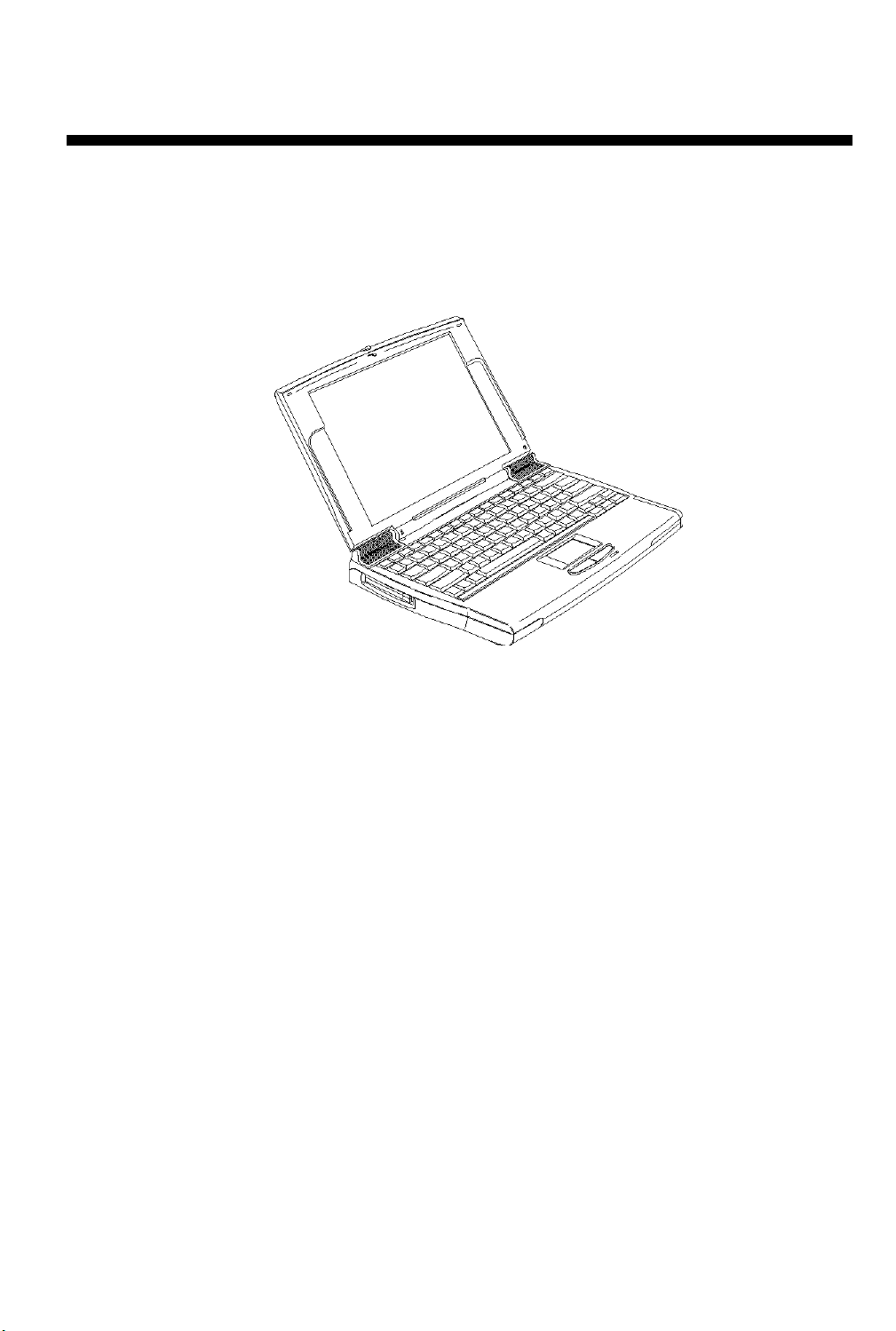
1.1 Overview
The notebook was designed with the user in mind. The figure below shows the notebook with the display
open.
Figure 1-1 Notebook
System Introduction 1-1
Page 20

1.1.1 Features
Here are just a few of the notebook’s many features:
Performance
• High-end Pentium microprocessor
• Support 64-bit main memory and external (L2) cache memory
• Large LCD display (DualScan STN and TFT active matrix.)
• PCI local bus video with graphics acceleration and 1MB video RAM boost video performance
• Internal 3.5-inch floppy drive or CD-ROM drive
• High-capacity, Enhanced-IDE hard disk
• Lithium-Ion or Nickel Metal-Hydride battery pack
• Power management system with standby and hibernation power saving modes
Multimedia
• 16-bit stereo audio with software wavetable
• Built-in dual speakers
• Ultra-slim, high-speed CD-ROM drive
Human-centric Design and Ergonomics
1
• Lightweight and slim
• Sleek, smooth and stylish design
• Full-sized keyboard
• Wide and curved palm rest
• Centrally-located touchpad pointing device
Expansion
• PC card (formerly PCMCIA) slots (two type II/I or one type III) with ZV (Zoomed Video) port support
• Upgradeable memory, hard disk, CPU
1
Some areas or regions may not offer models with a built-in CD-ROM drive.
1-2 Service Guide
Page 21
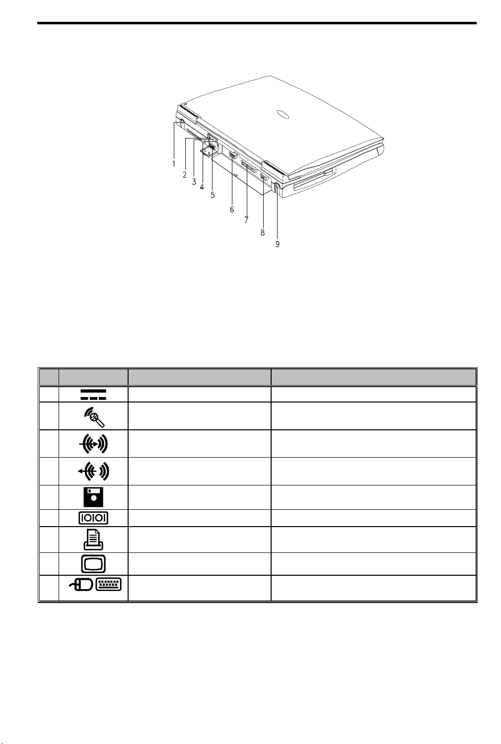
1.1.2 Rear Ports
1 DC-in Port 6 Serial Port
2 Microphone-in Port 7 Parallel Port
3 Line-in Port 8 External CRT Port
4 Line-out Port 9 PS/2 Port
5 External Floppy Drive Connector
Figure 1-2 Rear Ports
The following table describes these ports.
Table 1-1 Port Descriptions
# Icon Port Connects to...
1 DC-in Port AC adapter and power outlet
2 Microphone-in Port External 3.5mm minijack condenser microphone
3 Line-in Port Line-in device (e.g., CD player, stereo walkman)
4 Line-out Port Line-out device (e.g., speakers, headphones)
5 External Floppy Drive Connector External floppy drive
6 Serial Port Serial device (e.g., serial mouse)
7 Parallel Port Parallel device (e.g., parallel printer)
8 External CRT port Monitor (up to 1024x768, 256-colors )
9
PS/2 Port PS/2-compatible device
(e.g., PS/2 keyboard, keypad, mouse)
1.1.3 Indicator Light
A two-way indicator light is found on the inside and outside of the display. See figure below.
System Introduction 1-3
Page 22
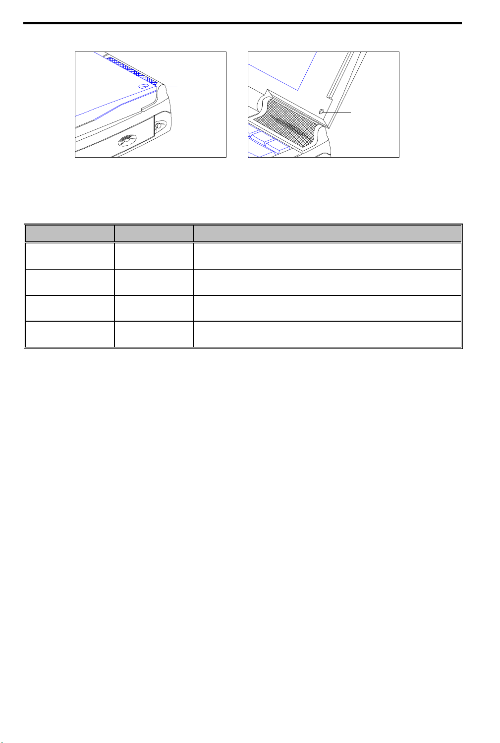
Indicator
Light
Indicator
Light
Figure 1-3 Indicator Light
This two-way indicator light allows you to see the notebook status when the display is open or closed. The
indicator serves both as a power and battery-charging indicator. See Table 1-2.
Table 1-2 Indicator Status Descriptions
Indicator Status Power Switch Condition
Green On
Red Off Battery is installed and a powered AC adapter is connected to the
Orange On Battery is installed and a powered AC adapter is connected to the
Flashing On Battery is running low on power and no AC adapter is connected to the
Charged battery is installed or a power AC adapter is connected to the
notebook.
notebook and charging the battery (rapid charge mode).
notebook and charging the battery (charge-in-use mode).
notebook.
1-4 Service Guide
Page 23

1.1.4 System Specifications Overview
Table 1-3 System Specifications
Item Standard Optional
Microprocessor Intel Pentium™ processor
(Intel P54CSLM 120/133/150 MHz)
System memory 8MB / 16MB
Dual 64-bit memory banks
Flash ROM BIOS 256KB
Data storage devices
CD-ROM model
FDD model
Display DualScan STN or TFT active matrix,
Video PCI local bus video with graphics
Audio 16-bit stereo audio; built-in dual
Keyboard and pointing
device
Removable 12.5mm, 2.5-inch, 1.0GB
Enhanced-IDE hard disk
Internal 15mm, 5.25-inch high-speed
CD-ROM drive
Internal 3.5-inch, 1.44MB floppy drive
800x600, 256 colors (SVGA)
accelerator and 1MB video RAM
speakers; separate audio ports
84-/85-/88-key with Windows 95 keys
Intel P55CLM - 133/150 with MMX
Expandable to 64MB using 8, 16 and 32MB
soDIMMs
1+GB Enhanced-IDE hard disk drive
External 3.5-inch, 1.44MB diskette drive
Up to 1024x768, 256-color ultra-VGA
monitor
LCD projection panel
101-/102-key, PS/2-compatible keyboard or
17-key numeric keypad
Touchpad (centrally-located on palmrest)
I/O ports One 9-pin RS-232 serial port
(UART16550-compatible)
One 25-pin parallel port
(EPP/ECP-compliant)
One 15-pin CRT port
One 6-pin PS/2 keypad/ keyboard/mouse
connector
One type III or two type II PC Card
slot(s) with ZV port support
One external FDD port
External serial or PS/2 mouse or similar
pointing device
Serial mouse, printer or other serial devices
Parallel printer or other parallel devices
Up to a 1024x768, 256-color
ultra-VGA monitor
17-key numeric keypad, PS/2 keyboard or
mouse
LAN card or other PC cards
External diskette drive
System Introduction 1-5
Page 24
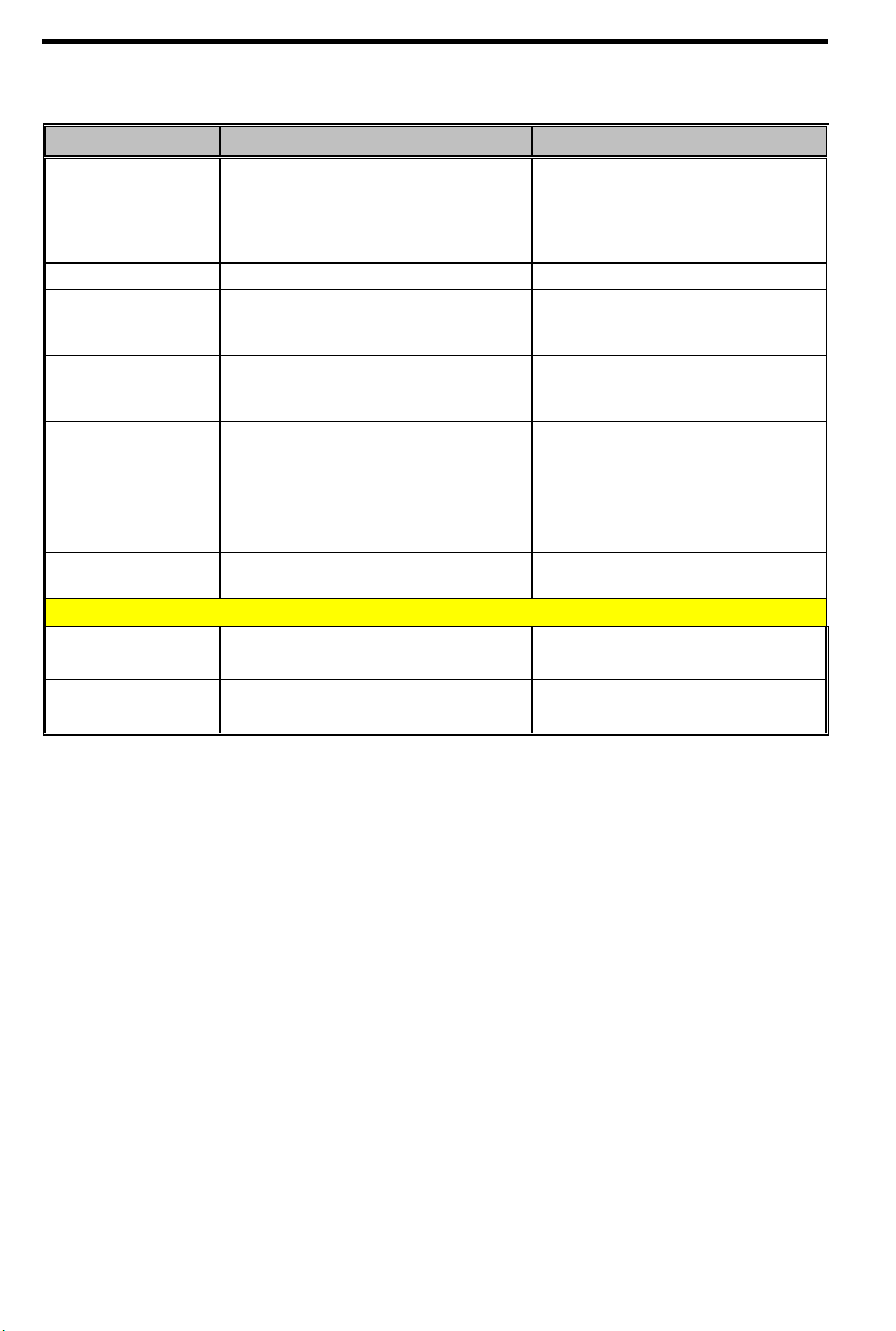
Table 1-3 System Specifications (continued)
Item Standard Optional
I/O ports (continued) One 3.5mm minijack mic-in port
Microphone
One 3.5mm minijack line-in port
One 3.5mm minijack line-out port
Operating system Windows 95 Windows 3.1
Weight
FDD model
CD-ROM model
Dimensions
(main footprint)
Temperature
Operating
Non-operating
Humidity
Operating
Non-operating
AC adapter 100~240 Vac, 50~60 Hz, 45W autosensing
Battery pack
Lithium-Ion 4-5 hr. (rapid-charge)
Nickel Metal-Hydride
battery
(includes battery)
2.6 kg. (5.7 lbs.)
2.8 kg. (6.2 lbs.)
W x D x H
306mm x 228mm x 46mm
(12.05” x 8.98” x 1.81”)
10ºC ~ 35ºC
-20ºC ~ 60ºC
(non-condensing)
20% ~ 80%
20% ~ 80%
AC adapter
6-8 hr. (charge-in-use)
2-2.5 hr. (rapid-charge)
5.5-6.5 hr. (charge-in-use)
Audio CD player or other line-in devices
Speakers or headphones
Extra AC adapter
Extra battery pack
External battery charger/discharger
Extra battery pack
External battery charger/discharger
1-6 Service Guide
Page 25
1.2 System Board Layout
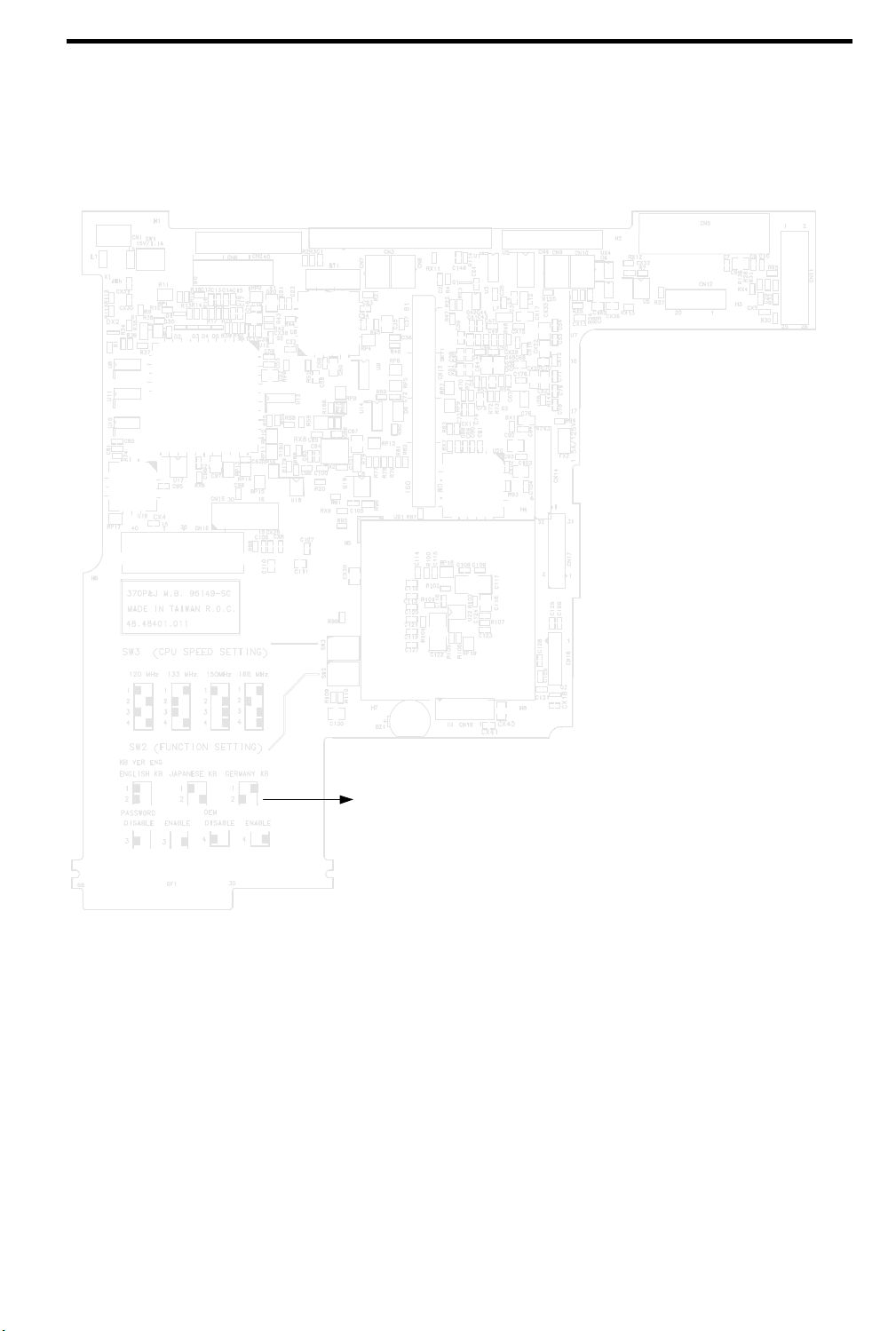
1.2.1 Main Board (PCB No: 96149-SC)
Note: This switch setting is not for Extensa 610 use.
Figure 1-4 Main Board Layout (Top Side)
System Introduction 1-7
Page 26
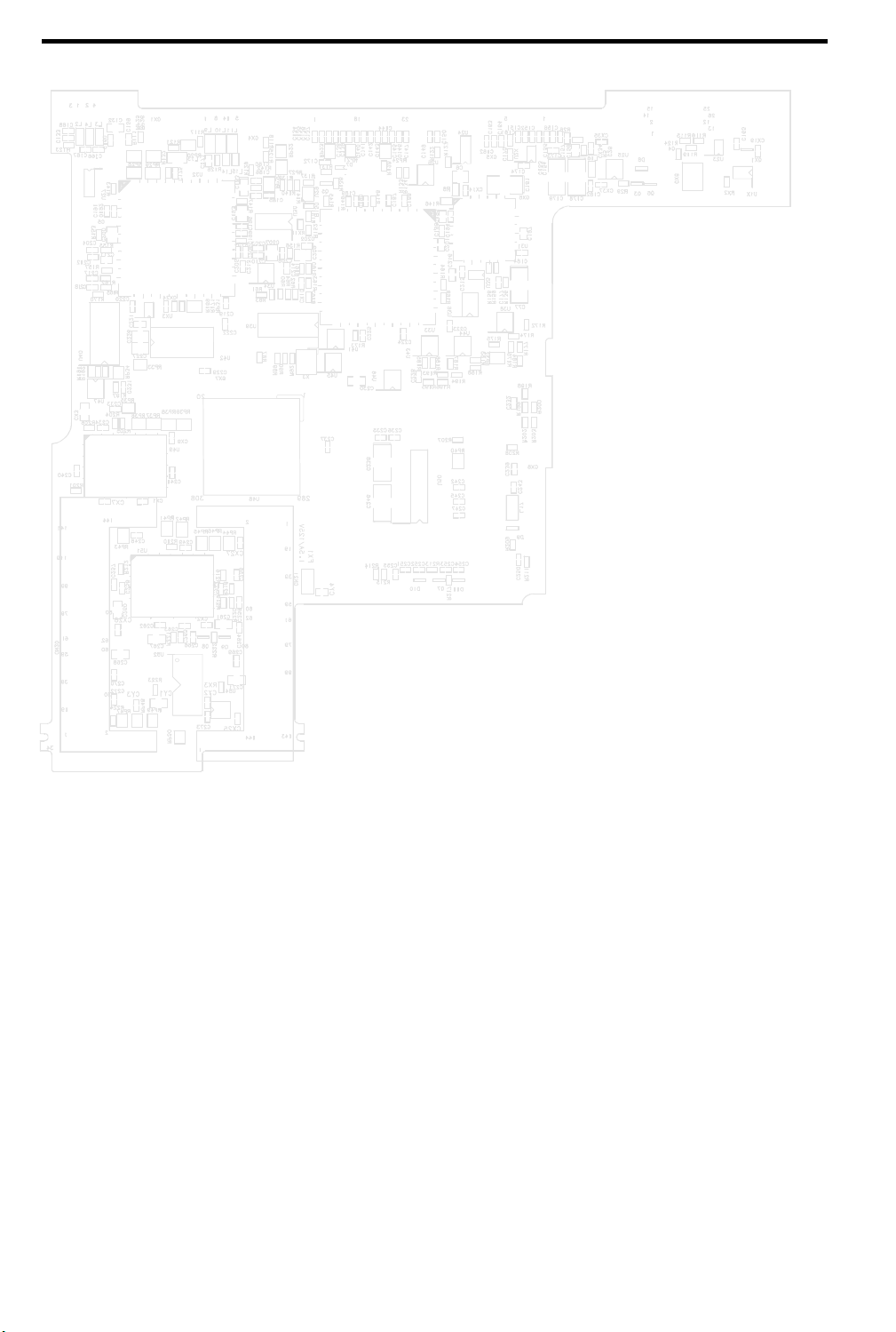
Figure 1-5 Main Board Layout (Bottom Side)
1-8 Service Guide
Page 27
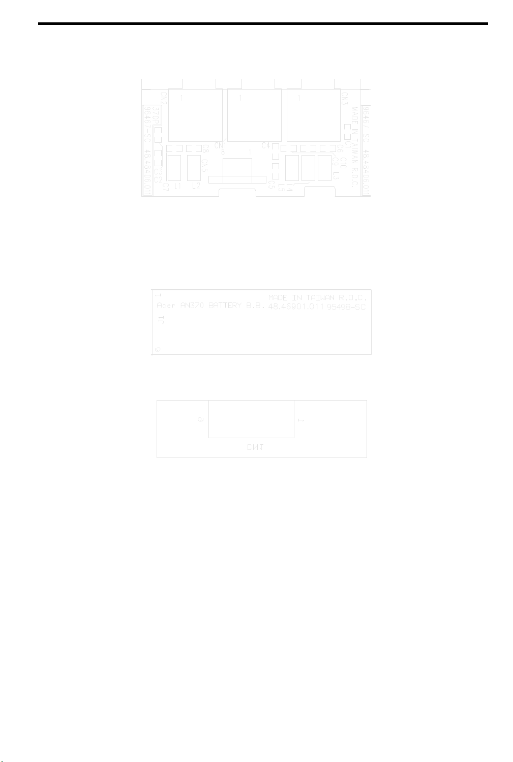
1.2.2 Audio Connection Board (PCB No:96467-1)
Figure 1-6 Audio Connection Board Layout (Top Side)
1.2.3 Battery Connection Board (PCB No:95498-1)
Figure 1-7 Battery Connection Board Layout (Top Side)
Figure 1-8 Battery Connection Board Layout (Bottom Side)
System Introduction 1-9
Page 28

1.2.4 HDD Connection Board (PCB No:96463-1)
Figure 1-9 HDD Connection Board Layout (Top Side)
Figure 1-10 HDD Connection Board Layout (Bottom Side)
1-10 Service Guide
Page 29

1.2.5 Keyboard Connection Board (PCB No: 96465-1)
Figure 1-11 Keyboard Connection Board Layout (Top Side)
Figure 1-12 Keyboard Connection Board Layout (Bottom Side)
System Introduction 1-11
Page 30
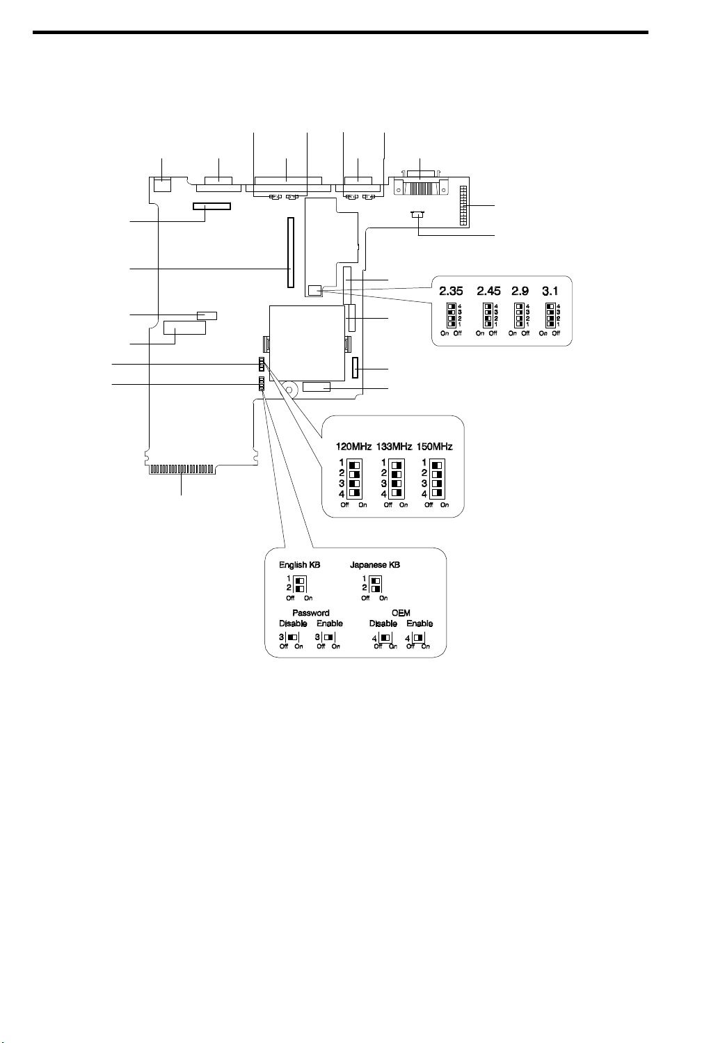
1.3 Jumpers and Connectors
Debug Card
CN13
CN15
CN16
SW3
SW2
CN1
CN6
Golden Finger for
CN2
CN7
CN3
CN8
CN9
CN4
CN10
CN14
CN17
CN18
CN19
CN5
CN11
CN12
S1
NOTE: The shaded area
(Black) indicates the position
of the switch.
CN1 External PS/2 keyboard/mouse port CN12 Audio Board Connector
CN2 VGA port CN13 PCMCIA socket connector
CN3 Parallel port CN14 Diskette Drive connector
CN4 Serial port CN15 HDD Connector
CN5 External floppy drive port CN16 Keyboard connector
CN6 LCD Connector CN17 CD-ROM connector
CN7 Audio speaker connector (left) CN18 Battery pack connector
CN8 LCD cover switch connector CN19 Track Point Board Connector
CN9 Fan connector S1 CPU Voltage Setting
CN10 Audio speaker connector (right) SW2 Function Setting
CN11 Charger Connector SW3 CPU Speed Setting
Figure 1-13 Jumpers and Connectors (Top View)
1-12 Service Guide
Page 31

Table 1-4 CPU Voltage (S1) Settings
CPU Voltage 2.35V 2.45V 2.9V 3.1V
Switch 1
Switch 2
Switch 3
Switch 4
Off Off Off Off
Off On Off Off
On Off Off Off
Off Off Off On
Table 1-5 CPU Speed (SW3) Settings
CPU Speed 120MHz 133MHz 150MHz
Switch 1
Switch 2
Switch 3
Switch 4
Off On Off
On Off On
Off Off On
On On On
Table 1-6 Multi-Function Switch (SW2) Settings
Switch ON OFF
1 Keyboard Type (Default OFF)
2 Keyboard Type
3 Password
4 Generic boot-up screen show on screen in
88-key (Japan keyboard) 84/85-key (U.S. keyboard)
- -
Bypass Check
No Yes
POST
System Introduction 1-13
Page 32

1.4 Hardware Configuration and Specification
1.4.1 Memory Address Map
Table 1-7 Memory Address Map
Address Range Definition Function
000000 - 09FFFF 640 KB memory Base memory
0A0000 - 0BFFFF 128 KB video RAM Reserved for graphics display buffer
0C0000 - 0CBFFF Video BIOS Video BIOS
0E0000 - 0EFFFF
128 KB system BIOS System BIOS
0F0000 - 0FFFFF
10000 - 7FFFF
80000 - 27FFF
FE0000 - FFFFFF 256 KB system ROM Duplicate of code assignment at 0E0000-0FFFFF
Extended memory Onboard Memory
System BIOS
SIMM memory
1.4.2 Interrupt Channel Map
Table 1-8 Interrupt Channel Map
Priority Interrupt Number Interrupt Source
1
2
3
4
5
6
7
8
9
10
11
12
13
14
15
16
17
SMI
NMI
IRQ 0
IRQ 1
IRQ 2
IRQ 8
IRQ 9
IRQ 10
IRQ 11
IRQ 12
IRQ 13
IRQ 14
IRQ 15
IRQ 3
IRQ 4
IRQ 5
IRQ 6
IRQ 7
Power management unit
Parity error detected, I/O channel error
Interval timer, counter 0 output
Keyboard
Interrupt from controller 2 (cascade)
Real-time clock
Cascaded to INT 0AH (IRQ 2)
Audio (option) / PCMCIA
Audio (option) / PCMCIA
PS/2 mouse
INT from coprocessor
Hard disk controller
CD-ROM controller
Serial communication port 2
Serial communication port 1
Parallel port (option) / Audio
Diskette controller
Parallel port (option)
A PCMCIA card can use IRQ 3, 4, 5, 7, 9 and 11 as long as it does not conflict with the
interrupt address of any other device.
1.4.3 DMA Channel Map
Table 1-9 DMA Channel Map
Controller Channel Address Function
1 0 0087 Audio (option)/ECP(option)
1-14 Service Guide
Page 33

1
1
1
2
2
2
2
1
2
3
4
5
6
7
1.4.4 I/O Address Map
Table 1-10 I/O Address Map
Address Range Device
000 - 00F
020 - 021
040 - 043
048 - 04B
060 - 064
070 - 071
080 - 08F
0A0 - 0A1
0C0 - 0DF
170 - 177
178, 17A
1F0 - 1F7
3F6, 3F7
220 - 22F, 240 - 24F
300 - 301, 330 - 331
370 - 371, 388 - 38F
530 - 537, E80 - E89
278 - 27F
2E8 - 2EF
2F8 - 2FF
378, 37A
3BC - 3BE
3B4, 3B5, 3BA
3C0 - 3C5
3C6 - 3C9
3C0 - 3CF
3D0 - 3DF
3E0 - 3E1
3E8 - 3EF
3F0 - 3F7
3F8 - 3FF
CF8 - CFF
DMA controller-1
Interrupt controller-1
Timer 1
Timer 2
Keyboard controller 38802 chip select
Real-time clock and NMI mask
DMA page register
Interrupt controller-2
DMA controller-2
CD-ROM
M7101 registers
Hard disk select
Audio (option) - default
Audio (option)
Audio (option)
Audio (option)
Parallel port 3
COM 4
COM 2
Parallel port 2
Parallel port 1
Video subsystem
Video DAC
Enhanced graphics display
Color graphics adapter
PCMCIA controller
COM3
Floppy disk controller
COM 1
PCI configuration register
0083
0081
0082
Cascade
008B
0089
008A
Audio
Diskette
Audio (option)/ECP(option)
Cascade
-
Spare
-
System Introduction 1-15
Page 34

1.4.5 M7101 GPIO (General Purpose I/O) Port Definition
Table 1-11 M7101 GPIO Port Definition
Item Description
GPIOA2 Smart inverter contrast counter control
GPIOA3 0: Normal operation of system
1: Shutdown system
GPIOA4 Serial data on X24C02
GPIOA5 Battery gauge communication control
GPIOA6 Battery data line
GPIOA7 Thermal sensor data line
GPIOC6 VGA thermal sensor data line
GPIOC7 0: VGA chip standby mode
1: Normal operation
Register E0h bit 8 Serial clock on X24C02
Register E0h bit 9 0: Disable 12V for flash ROM
1: Enable 12V for flash ROM
Register E0h bit 10 0: 3 mode FDD
1: Normal
Register E0h bit 11 Thermal sensor clock line
Register E0h bit 12 Thermal sensor reset
Register E0h bit 13 0: Enable battery LED
1: Disable battery LED
Register E0h bit 14 0: Disable audio amplifier
1: Enable audio amplifier
Register E1h bit 0 0: NiMH battery
1: Li-ion battery
Register E1h bit 1 CPU thermal high
1.4.6 Processor
Table 1-12 Processor Specifications
Item Specification
CPU type P54CSLM-120,P54CSLM-133, P54CSLM-150, P55CLM-133,
P55CLM - 150
CPU package SPGA
Switchable processor speed (Y/N) Yes
Minimum working speed 0MHz while hibernation mode
CPU voltage 3.1V/2.9V/2.45V
1.4.7 BIOS
Table 1-13 BIOS Specifications
1-16 Service Guide
Page 35

Item Specification
BIOS vendor Acer
BIOS version v2.1
BIOS in flash EPROM (Y/N) Yes
BIOS ROM size 256KB
BIOS package type 32-pin TSOP
Same BIOS for STN color/TFT color (Y/N) Yes
The BIOS can be overwritten/upgradeable using the “AFLASH” utility (AFLASH.EXE).
Please refer to software specification section for details.
1.4.8 System Memory
Memory is upgradeable from 8 to 64 MB, employing 8-/16-/32-MB 64-bit soDIMMs (Small Outline Dual
Inline Memory Modules). After installing the memory modules, the system automatically detects and
reconfigures the total memory size during the POST routines. The following lists important memory
specifications.
• Memory bus width: 64-bit
• Expansion RAM module type:144-pin, 64-bit, small outline Dual Inline Memory Module (soDIMM)
• Expansion RAM module size/configuration:
• 8MB (1M*16 x4)
• 16MB (2M*8 x8)
• 32MB (4M*16 x4)
• Expansion RAM module speed/voltage/package: 60ns/3.3v/TSOP EDO
• EDO and fast-page mode DIMMs may be used together in a memory configuration.
System Introduction 1-17
Page 36

The following table lists all possible memory configurations.
Table 1-14 Memory Configurations
Slot 1 Slot 2 Total Memory
8 MB 0 MB 8 MB
0 MB 8 MB 8 MB
8 MB 8 MB 16 MB
16 MB 0 MB 16 MB
0 MB 16 MB 16 MB
16 MB 8 MB 24 MB
8 MB 16 MB 24 MB
16 MB 16 MB 32 MB
32 MB 0 MB 32 MB
0 MB 32 MB 32 MB
32 MB 8 MB 40 MB
8 MB 32 MB 40 MB
32 MB 16 MB 48 MB
16 MB 32 MB 48 MB
32 MB 32 MB 64 MB
1.4.9 Second-Level Cache
This notebook supports 256KB pipeline burst second-level (L2) cache.
1-18 Service Guide
Page 37

1.4.10 Video Memory
Table 1-15 Video RAM Configuration
Item Specification
DRAM or VRAM DRAM(EDO type)
Fixed or upgradeable Fixed
Memory size/configuration 1MB (256K x 16 x 2pcs)
Memory speed 60ns
Memory voltage 3.3V
Memory package TSOP
1.4.11 Video
Table 1-16 Video Hardware Specification
Item Specification
Video chip C&T65550B
Working voltage C&T65550B: 3.3V
C&T65550XX: 3.3V/5V (“XX” represents codes other than “A” (i.e. “B1”))
Video Chip substitutability Yes
During power-on, system supplies 5V to video chip and read its register to determine
whether the video chip is 5V or 3.3V/5V type. If 5V video chip is detected, system
maintains video voltage at 5V; if 3.3V/5V video chip is detected, system switches
video voltage to 3.3V.
1.4.11.1 External CRT Resolution Support
Table 1-17 Supported External CRT Resolutions
Resolution x Color on
External CRT
640x480x16 60,75,85 60 Y Y
640x480x256 60,75,85 60 Y Y
640x480x65,536 60,75,85 60 Y Y
640x480x16,777,216 60,75,85 60 Y N
800x600x16 56,60,75 60 Y Y
800x600x256 56,60,75 60 Y Y
800x600x65,536 56,60 60 Y N
1024x768x16 60,75,86I 60 Y Y
CRT Refresh Rate Simultaneous on
TFT LCD
CRT only Simultaneous SVGA SVGA
Simultaneous on
STN LCD
Table 1-17 Supported External CRT Resolutions (Continued)
Resolution x Color on
External CRT
1024x768x256 60,75,86I 60 Y Y
CRT Refresh Rate Simultaneous on
TFT LCD
Simultaneous on
STN LCD
System Introduction 1-19
Page 38

1280x1024x16 86I 60 Y Y
1.4.11.2 LCD Resolution Support
Table 1-18 Supported LCD Resolutions
Resolution x Color on LCD Only TFT LCD (SVGA) STN LCD (SVGA)
640x480x16 Y Y
640x480x256 Y Y
640x480x65,536 Y Y
640x480x16,777,216 Y 800x600x16 Y Y
800x600x256 Y Y
800x600x65,536 Y 1024x768x16 Y Y
1024x768x256 Y Y
• DSTN color number: 256 colors
• TFT color number: 65536 colors
• Maximum resolution (LCD Panel): 800x600
• Maximum resolution (External CRT): 1280x1024
Using software, you can set the LCD to a higher resolution than its physical resolution, but
the image shown on the LCD will pan.
1-20 Service Guide
Page 39

1.4.12 Parallel Port
Table 1-19 Parallel Port Configurations
Item Specification
Number of parallel ports 1
ECP/EPP support Yes (set by BIOS setup)
Connector type 25-pin D-type
Location Rear side
Selectable parallel port (by BIOS Setup)
• Parallel 1 (3BCh, IRQ7)
• Parallel 2 (378h, IRQ7)
• Parallel 3 (278h, IRQ5)
• Disable
1.4.13 Serial Port
Table 1-20 Serial Port Configurations
Item Specification
Number of serial ports 1
16550 UART support Yes
Connector type 9-pin D-type
Location Rear side
Selectable serial port (by BIOS Setup)
• Serial 1 (3F8h, IRQ4)
• Serial 2 (2F8h, IRQ3)
• Disable
System Introduction 1-21
Page 40

1.4.14 Audio
Table 1-21 Audio Specifications
Item Specification
Chipset YMF715
Audio onboard or optional Built-in
Mono or stereo Stereo
Resolution 16-bit
Compatibility SB-16 , Windows Sound System
Mixed sound sources Voice, Synthesizer, Line-in, Microphone, CD
Voice channel 8-/16-bit, mono/stereo
Sampling rate 44.1 kHz
Internal microphone No
Internal speaker / quantity Yes / 2 pcs.
Microphone jack Yes
Headphone jack Yes
1.4.15 PCMCIA
PCMCIA is an acronym for Personal Computer Memory Card International Association. The PCMCIA
committee set out to standardize a way to add credit-card size peripheral devices to a wide range of personal
computers with as little effort as possible.
There are two type II/I or one type III PC Card slots found on the left panel of the notebook. These slots
accept credit-card-sized cards that enhances the usability and expandability of the notebook.
ZV (Zoomed Video) port support allows your system to support hardware MPEG in the form of a ZV PC
card.
Table 1-22 PCMCIA Specifications
Item Specification
Chipset TI 1131
Supported card type Type-II / Type-III
Number of slots Two Type-II or one Type-III
Access location Left side
ZV (Zoomed Video) port support Yes (only in lower slot)
1-22 Service Guide
Page 41

1.4.16 Touchpad
Table 1-23 Touchpad Specifications
Item Specification
Vendor & model name
Power supply voltage (V) 5 ± 10%
Location Palm-rest center
Internal & external pointing device work simultaneously Yes
Support external pointing device hot plug Yes
X/Y position resolution (points/mm) 20
Interface PS/2 (compatible with Microsoft mouse driver)
Synaptics TM1002MPU
1.4.17 Keyboard
Table 1-24 Keyboard Specifications
Item Specification
Vendor & model name SMK KAS1901-0161R (English)
Total number of keypads 84/85 keys
Windows 95 keys Yes, (Logo key / Application key):
Internal & external keyboard work simultaneously Yes
1.4.17.1 Windows 95 Keys
The keyboard has two keys that perform Windows 95-specific functions. See Table 1-26.
Table 1-25 Windows 95 Key Descriptions
Key Description
Windows logo key Start button. Combinations with this key performs special functions. Below are a few
examples:
• Windows + Tab Activate next Taskbar button
• Windows + E Explore My Computer
• Windows + F Find Document
• Windows + M Minimize All
• Shift + Windows + M Undo Minimize All
• Windows + R Display Run dialog box
Application key Opens the application’s context menu (same as right-click).
System Introduction 1-23
Page 42

1.4.18 FDD
Table 1-26 FDD Specifications
Item Specification
Vendor & model name Mitsumi D353F2
Floppy Disk Specifications
Media recognition 2DD (720K) 2HD (1.2M, 3-mode) 2HD (1.44M)
Sectors / track 9 15 18
Tracks 80 80 80
Data transfer rate (Kbits/s) 250 300 500 500
Rotational speed (RPM) 300 360 360 300
Read/write heads 2
Encoding method MFM
Power Requirement
Input Voltage (V) +5 ± 10%
1.4.19 HDD
Table 1-27 HDD Specifications
Item Specification
Vendor & Model Name IBM DMCA21080 IBM DMCA21440 IBM DTNA22160 Toshiba
MK1002MAV
Drive Format
Capacity (MB) 1080 1440 2160 1085
Bytes per sector
Logical heads
Logical sectors
Logical cylinders 2100 2800 4200 2100
Physical read/write heads 3
Disks
Spindle speed (RPM) 4009 4009 4000 4635
Performance Specifications
Buffer size (KB) 128 96 96 128
Interface ATA-3 ATA-3 ATA-3 ATA-3
Data transfer rate
(disk-buffer, Mbytes/s)
512 512
16 16
63 63
4
2 2
39.5 ~ 61.8 39.5 ~ 61.8 39.1~ 61.6 29.3 ~ 55.5
512 512
16 16
63 63
6 6
3 3
1-24 Service Guide
Page 43

Item Specification
Performance Specifications
Data transfer rate
(host-buffer, Mbytes/s)
DC Power Requirements
Voltage tolerance (V)
16.6 (max., PIO
mode 4)
5 ± 5%
16.6 (max., PIO
mode 4)
5 + 5%, -10%
16.6 (max., PIO
mode 4)
5 ± 5% 5 ± 5%
1.4.20 CD-ROM
Table 1-28 CD-ROM Specifications
Item Specification
Vendor & Model Name
Performance Specification
Speed (KB/sec) 150 (normal speed)
Access time (ms) 170 (Typ.)
Buffer memory (KB) 128
Interface Enhanced IDE (ATAPI) compatible
Applicable disc format CD-DA, CD-ROM, CD-ROM XA (except ADPCM), CD-I,
Loading mechanism Drawer type, manual load/release
Power Requirement
Input Voltage (V) 5
Panasonic UJDCD8730
1500 (10X speed)
Photo CD (Multisession), Video CD, CD+
16.6 (max., PIO
mode 4)
1.4.21 Battery
Table 1-29 Battery Specifications
Item Specification
Battery gauge on screen Yes, by hotkey Yes, by hotkey Yes, by hotkey
Vendor & model name Sanyo BTP-W31 Sony BTP-T31 Toshiba BTP-X31
Battery type NiMH Li-Ion NiMH
Cell capacity (mAH) 3500 4050 3500
Cell voltage (V) 1.2 3.6 1.2
Number of battery cell 9-cell 9-Cell 9-Cell
Package configuration 9 serial 3 serial, 3 parallel 9 serial
Package voltage (V) 10.8 10.8 10.8
Package capacity (WAH) 37.8 40.5 37.8
System Introduction 1-25
Page 44

1.4.22 Charger
To charge the battery, place the battery pack inside the battery compartment and plug the AC adapter into
the notebook and an electrical outlet. The adapter has three charging modes:
• Rapid mode
The notebook uses rapid charging when power is turned off and a powered AC adapter is connected to
it. In rapid mode, a fully depleted battery gets fully charged in approximately two hours.
• Charge-in-use mode
When the notebook is in use with the AC adapter plugged in, the notebook also charges the battery
pack if installed. This mode will take longer to fully charge a battery than rapid mode. In charge-inuse mode, a fully depleted battery gets fully charged in approximately six to eight hours.
• Trickle mode
When the battery is fully charged, the adapter changes to trickle mode to maintain the battery charge
level. This prevents the battery from draining while the notebook is in use.
Table 1-30 Charger Specifications
Item Specification
Vendor & model name Ambit T62.062.C.00
Input voltage (from adapter, V) 19 (min.)
20 (typ.),
20.5 (max.)
Battery Low Voltage
Battery Low 1 level (V) 10.7 (typ., for NiMH)
8.65 (typ., for LIB)
Battery Low 2 level (V) 10.35 (typ., for NiMH)
8.23 (typ., for LIB)
Battery Low 3 level (V) 9.22 (typ., for NiMH)
7.73 (typ., for LIB)
Charge Current
Fast charge (charge when system is still operative, A) 0.65 (typ.)
Quick charge (charge while system is not operative, A) 1.9 (typ.)
Charging Protection
Safety timer for Fast Charge mode while notebook is operating (minute) 576 (NiMH)
Safety timer for Quick Charge mode while notebook is not operating (minute) 192 (NiMH)
Maximum temperature protection (ºC) 60
Maximum voltage protection (V) 16.2V for NiMH
Over voltage protection 13V for Li-ion
1.4.23 DC-DC Converter
DC-DC converter generates multiple DC voltage level for whole system unit use.
Table 1-31 DC-DC Converter Specifications
1-26 Service Guide
Page 45

Item Specification
Vendor & model name Ambit T62.061.C.00
Input voltage (Vdc) 8~21
Output Rating 5V 3.3V 2.9V
(2.35/2.45/2.9/3.1V)
Current (w/ load, A) 0~3.2 0~3.3 0~3.0 0~0.15 0~0.1 0.005
Voltage ripple (max., mV) 75 75 50 100 300 75
Voltage noise (max., mV) 100 100 100 200 500 100
OVP (Over Voltage Protection, V) 6.5~8.2 4.5~6.2 3.3~5.0 for
2.9/3.1/2.35V/2.45V
+12V +6V 5VSB
14~20 7~9 -
1.4.24 DC-AC Inverter
DC-AC inverter is used to generate very high AC voltage, then supply to LCD CCFT backlight use, and is
also responsible for the control of LCD brightness. Avoid touching the DC-AC inverter area while the
system unit is turned on.
Table 1-32 DC-AC Inverter Specifications
Item Specification
Vendor & model name Ambit T62.066.C.00 / Ambit T62.064.C.00
Input voltage (V) 7.3 (min.) - 20 (max.)
Input current (mA) - 420 (typ.) 550 (max.)
Output voltage (Vrms, no load) 1000 (min.) - 1500 (max.)
Output voltage frequency (kHz) 25 (min.) 42 (typ.) 60 (max.)
Output current (mArms) 1.5~5.5 (min.) 2.0~6.0 (typ.) 2.5~6.5 (max.)
System Introduction 1-27
Page 46

1.4.25 LCD
Table 1-33 LCD Specifications
Item Specification
Vendor & model name HITACHI
LMG9900ZWCC
Mechanical Specifications
LCD display area
(diagonal, inch)
Display technology STN STN TFT TFT
Resolution SVGA (800x600) VGA (800x600) SVGA (800x600) SVGA (800x600)
Supported colors -- -- 262,144 colors 262,144 colors
Optical Specification
Contrast ratio 30 (typ.) 30 (typ.) 100 (typ.) 100 (typ.)
Brightness (cd/m2)
Brightness control keyboard hotkey keyboard hotkey keyboard hotkey keyboard hotkey
Contrast control using keyboard
Electrical Specification
Supply voltage for LCD
display
Supply voltage for LCD
backlight (Vrms)
11.3 11.3 11.3 12.1
70 (typ.) 70 (typ.) 70 (typ.) 70 (typ.)
hotkey
3.3 or 5 (typ.) 3.3 (typ.) 3.3 3.3 (typ.), 3.63
590 (typ.) 590 (typ.) 590 480
TORiSAN
LM-FH53-22NAW
using keyboard
hotkey
IBM
ITSV45E
none none
GOLDSTAR
LP121S1-J
(max.)
The LCD ID code can be set by using the LCD ID utilization utility
(370pw.exe/370pr.exe). Please refer to the software specification section for details.
1-28 Service Guide
Page 47

1.4.26 AC Adapter
Table 1-34 AC Adapter Specifications
Item Specification
Vendor & model name Delta ADP-45GB REV.E2
Input Requirements
Nominal voltages (Vrms) 90 - 264
Frequency variation range (Hz) 47 - 63
Maximum input current (A, @90Vac, full load) 1.5 A
Inrush current The maximum inrush current will be less than 50A and 100A
when the adapter is connected to 115Vac(60Hz) and
230Vac(50Hz) respectively.
Efficiency It should provide an efficiency of 83% minimum, when
measured at maximum load under 115V(60Hz)
Output Ratings (CV mode)
DC output voltage (V) +19
Noise + Ripple (mV) 300
Load (A) 0 (min.) 2.4 (max.)
Dynamic Output Characteristics
Turn-on delay time (s, @115Vac) 2
Hold up time (ms; @115 Vac input, full load) 5 (min.)
Over Voltage Protection (OVP, V) 26
Short circuit protection Output can be shorted without damage
Electrostatic discharge (ESD, kV) ±15 (at air discharge)
Dielectric Withstand Voltage
Primary to secondary 3000 Vac (or 4242 Vdc), 10 mA for 1 second
Leakage current 0.25 mA maximum @ 254 Vac, 60Hz.
Regulatory Requirements
Internal filter meets:
1. FCC class B requirements.
2. CISPR 22 Class B requirements.
System Introduction 1-29
Page 48

1.5 Software Configuration and Specification
1.5.1 BIOS
The BIOS is compliant to PCI v2.1, APM v1.2, E-IDE and PnP specification. It also defines the hotkey
functions and controls the system power-saving flow.
1.5.1.1 Keyboard Hotkey Definition
The notebook supports the following hotkeys.
Table 1-35 Hotkey Descriptions
Hotkey
Fn-Esc Hotkey Escape Exits the hotkey control.
Fn-F1
Fn-F2 Brightness Control
Fn-F3 Display Toggle Switches display from LCD to CRT to both LCD and CRT.
Fn-F4 Battery Gauge Displays the battery gauge.
Fn-F5 Volume Control
Fn-F6 Setup Gains access to BIOS Setup’s Advanced System Configuration
Fn-F7 Hibernation/Standby Enters hibernation mode if the 0-volt suspend function is installed
Fn-→
Fn-←
Fn-T Toggle Touchpad Turns the internal touchpad on and off.
Icon Function Description
Hotkey Help
?
Contrast Control
Scale Increase Increases the setting of the current icon.
Scale Decrease Decreases the setting of the current icon.
Displays the hotkey list and help. Press | to exit the screen.
Toggles between brightness control and contrast control.
Press the scale hotkeys (Fn- →and Fn -←) to increase and decrease
the brightness or contrast level.
Notebooks with TFT displays do not show the brightness control
icon.
Press the scale hotkeys (Fn-→ and Fn-←) to increase and decrease
the output level.
parameters.
and enabled; otherwise, the notebook enters standby mode.
When the available hotkey is toggled, the system will issue a beep to enter the assigned
process.
1.5.1.2 MultiBoot
The system can boot from the FDD, External FDD, HDD, CD-ROM. The user can select the desired
booting process to boot the system. If the CD-ROM is bootable, the BIOS will override the other process to
boot the system directly.
1-30 Service Guide
Page 49

1.5.1.3 Power Management
Figure 1-14 Power Management Block Diagram
System Introduction 1-31
Page 50

ON MODE
Normal full-on operation
STANDBY MODE
The notebook consumes very low power in standby mode. Data remain intact in the system memory until
battery is drained.
The necessary condition for the notebook to enter standby mode is that the reserved disk space size for
saving system and video memory is insufficient so the notebook is unable to enter hibernation mode. In this
situation, there are three ways to enter standby mode:
• Press the standby/hibernation hotkey
Fn-F7
( )
• Set a value for the System Standby/Hibernation Timer in Setup. If the waiting time specified by this
timer elapses without any system activity, the notebook goes into standby mode.
• Invoked by the operating system power saving modes
The following signals indicate that the notebook is in standby mode:
• The buzzer beeps (when you press the standby/hibernation hotkey)
• The indicator light flashes
To leave standby mode and return to normal mode, press the any key. If an incoming PCMCIA modem
event occurs and the Modem Ring Wake Up From Standby is enabled, the system returns to normal mode.
Table 1-36 Standby Mode Conditions and Descriptions
Condition Description
The condition to enter
Standby Mode
The condition of
Standby Mode
The condition back to
On Mode
• “Hard Disk Drive” is [Disabled] in System Security of BIOS SETUP.
• “Hard Disk 0” is [None] in Basic System Configuration of BIOS SETUP.
• HDD has not located enough free contiguous disk space generated by Sleep Manager
and this free space is not corrupted.
• Standby/Hibernation Timer times-out or Standby/Hibernation HotKey pressed and
there is no activity within 1/2 second.
• Issue a beep.
• Flash standby LED with 1 Hz frequency.
• Disable the mouse, serial and the parallel port.
• The keyboard controller, HDD and VGA enter the standby mode.
• Stop the CPU internal clock.
• All the functions are disabled except the keyboard, battery low warning and modem
ring wake up from standby (if enabled).
Any one of following activities will let system back to Normal Mode:
• Any keystroke (Internal KB or External KB)
• Modem ring.
HIBERNATION MODE
In hibernation mode (also known as zero-volt hibernation-to-disk mode), power shuts off. The notebook
saves all system information onto the hard disk before it enters hibernation mode. Once you turn on the
power, the notebook restores this information and resumes where you left off upon leaving hibernation
mode.
1-32 Service Guide
Page 51

A necessary condition for the notebook to enter hibernation mode is that the reserved space for saving
system information on the hard disk must be larger than the combined system and video memory size.
Under such conditions, the standby/hibernation hotkey acts as the hibernation hotkey. See the user’s
manual for information on the Sleep Manager utility.
In this situation, there are four ways to enter hibernation mode:
• Press the standby/hibernation hotkey
Fn-F7
( )
• Set a value for the System Standby/Hibernation Timer in Setup. If the waiting time specified by this
time elapses without any system activity, the system goes into hibernation mode
• Enable the Suspend upon Battery-low parameter in Setup. If a battery-low condition takes place, the
notebook enters hibernation mode in about five minutes.
• Invoked by the operating system power saving modes
When the notebook enters hibernation mode, the whole system does not consume any power. This is why
hibernation mode is also called zero-volt suspend.
To exit hibernation mode, press the power switch ( ).
When the PCMCIA I/O card is detected, the following warning pop-up message will be
displayed on the screen by the BIOS. The system will wait for the specified key to continue.
Warning!!
A PCMCIA card is detected!!
If you are using a fax/modem or LAN cards, please
disconnect with server or complete transmission before
entering standby/hibernation mode, otherwise :
1) File server will be shut down if LAN card is used.
2) Data will be lost if a modem card is used.
Press <F1> to enter standby/hibernation mode.
Press <F2> to cancel.
System Introduction 1-33
Page 52

Table 1-37 Hibernation Mode Conditions and Descriptions
Condition Description
The condition to enter
Hibernation Mode
The condition of
Hibernation Mode
The condition back to On
Mode
DISPLAY STANDBY MODE
• “Hard Disk Drive” is not [Disabled] in System Security of BIOS SETUP.
• “Hard Disk 0” is not [None] in Basic System Configuration of BIOS SETUP.
• HDD has already located enough free contiguous disk space generated by the
Sleep Manager and this free space is not corrupted.
• Standby/Hibernation Timer times-out or Standby/Hibernation Hotkey pressed and
there is no activity within 1/2 second.
• Except the RTC, 6375 (state machine), KB controller and power switch, all the
system components are off.
• Turn off then on the system.
Screen activity is determined by the keyboard, the built-in touchpad, and an external PS/2 pointing device.
If these devices are idle for the period specified by the Display Standby Timer, the display shuts off until you
press a key or move the touchpad or external mouse.
Table 1-38 Display Standby Mode Conditions and Descriptions
Condition Description
The condition to enter
Display Standby Mode
The condition of Display
Standby Mode
The condition back to On
Mode
• Pointing device is idle until Display Standby Timer times-out or LCD cover is
closed.
• All the system components are on except LCD backlight and CRT horizontal
frequency output (if CRT is connected)
• Any keystroke (Internal KB or External KB)
• Pointing device activity
The VGA BIOS should support DPMS (Desktop Power Management System) for the standby
and hibernation mode function call. When the Display Standby Timer expires, the system
BIOS will execute the DPMS service routines.
HARD DISK STANDBY MODE
The hard disk enters standby mode when there are no disk read/write operations within the period of time
specified by the Hard Disk Standby Timer. In the standby state, the power supplied to the hard disk is
reduced to a minimum. The hard disk returns to normal once the system accesses it.
1-34 Service Guide
Page 53

Table 1-39 Hard Disk Standby Mode Conditions and Descriptions
Condition Description
The condition to enter HDD Standby
Mode
The condition of HDD Standby Mode
The condition back to On Mode
BATTERY LOW
When the battery capacity is low and has no adapter plugged, the system will generate the following battery
low warning:
• Display Standby Timer times-out or LCD cover is closed.
• All the system components are on except HDD spindle motor
• Any access to HDD
• Flash power LED with 4 Hz.
• Issue 4 short beeps per minute (if enabled in setup).
• If the AC adapter does not plug in within 3 minutes and the “Standby/Hibernation upon Battery-low”
in BIOS SETUP is enabled, the system will enter Standby/0-Volt Hibernation Mode. The battery low
warning will stop as soon as the AC adapter is plugged into the system.
THE AUTODIM PROCESS OF THE LCD BRIGHTNESS
The notebook has a unique “automatic dim” power saving feature. When the notebook is using AC power
and you disconnect the AC adapter from the notebook, the system “decides” whether or not to automatically
dim the LCD backlight to save power.
If the LCD backlight is too bright, the system automatically adjusts it to a manageable level; otherwise, the
level stays the same. If you want a brighter picture, you can then adjust the brightness and contrast level
using hotkeys (Fn-F2).
If you reconnect AC power to the system, the system automatically adjusts the LCD backlight to its original
level — the brightness and contrast level before disconnecting the AC adapter. If you adjusted the
brightness and contrast level after disconnecting AC power, the level stays the same after you reconnect the
AC adapter.
There are two reasons for the notebook to have the LCD AutoDim feature. The first is to save the power
during the notebook is operating under the DC mode. The second is to save the “favorite” brightness
parameter set by the user.
The following processes are the basic methods used to implement the LCD brightness AutoDim.
1. If the original brightness is over 75% and the AC power is on-line, the BIOS will change the brightness
to 75% after the AC power is off-line.
2. If the original brightness is below 75%, the brightness maintains the same level even if the AC power is
off-line.
3. If the brightness is already changed by the hotkey under DC power, it will not be changed after the AC
power is plugged in.
4. If the brightness is not changed by the hotkey under DC power, the brightness will be changed back to
the old setting — the previous brightness parameter under AC power.
5. If the previous brightness parameter does not exist, the brightness will not be changed in process 4.
System Introduction 1-35
Page 54

1.5.2 Drivers, Applications and Utilities
The notebook comes preloaded with the following software:
• Windows 95
• System utilities and application software
2
3
• Sleeper manager utility
• Touchpad driver
• Display drivers
• Audio drivers
• PC Card slot drivers and applications
• Other third-party application software
Table 1-40 Location of Drivers in the System Utility CD
Device Category Function Location
Sound, video and game controllers Audio ENGLISH\WIN95\AUDIO\
Mouse Mouse ENGLISH\WIN95\MOUSE\
Display adapters Video ENGLISH\WIN95\VGA\
PCMCIA Zoomed Video Port English\Win95\PCMCIA\
To re-install applications under Windows 95, click on Start, then Run…. Based on the location of the
application, run the setup program to install the application. The following table lists the applications and
their locations:
Table 1-41 Location of Applications in the System Utility CD
Name Function Location
Sleep Manager 0V Suspend utility ENGLISH\WIN95\SLEEPMGR\
Y-Station Audio application ENGLISH\WIN95\Ystation
SafeOFF Protect if user accidentally
press the power switch
ENGLISH\WIN95\SAFEOFF
Drivers for Windows 3.x and Windows NT are also found in the System Utility CD if you should need
them.
2
In some areas, a different operating system may be pre-loaded instead of Windows 95.
3
The system utilities and application software list may vary.
1-36 Service Guide
Page 55

1.6 System Block Diagram
Figure 1-15 System Block Diagram
System Introduction 1-37
Page 56

1.7 Environmental Requirements
Table 1-42 Environmental Requirements
Item Specification
Temperature
Operating (ºC)
Non-operating(ºC)
Humidity
Operating (non-condensing) 20% ~ 80%
Non-operating (non-condensing) 20% ~ 80%
Operating Vibration (unpacked)
Operating 5 - 25.6Hz, 0.38mm; 25.6 - 250Hz, 0.5G
Sweep rate > 1 minute / octave
Number of test cycles 2 / axis (X,Y,Z)
Non-operating Vibration (unpacked)
Non-operating 5 - 27.1Hz, 0.6G; 27.1 - 50Hz, 0.41mm; 50~500Hz, 2G
Sweep rate > 2 minutes / octave
Number of text cycles 4 / axis (X,Y,Z)
Shock
Non-operating (unpacked) 40G peak, 11±1ms, half-sine
Non-operating (packed) 50G peak, 11±1ms, half-sine
Altitude
Operating 10,000 feet
Non-operating 40,000 feet
ESD
Air discharge 8kV (no error)
Contact discharge 4kV (no error)
+5°C ~ +35°C
-20°C ~ +60°C
12.5kV (no restart error)
15kV (no damage)
6kV (no restart error)
8kV (no damage)
1-38 Service Guide
Page 57

1.8 Mechanical Specifications
Table 1-43 Mechanical Specifications
Item Specification
Weight
FDD model
CD-ROM model
Dimensions
(main footprint)
(includes battery)
2.6 kg. (5.7 lb.)
2.8 kg. (6.2 lb.)
W x D x H
306mm x 228mm x 46mm (12.05” x 8.98” x 1.81”)
System Introduction 1-39
Page 58

C h a p t e r 2C h a p t e r 2
Major Chips Description
This chapter discusses the major chips used in the notebook.
2.1 Major Component List
Table 2-1 Major Chips List
Component Vendor Description
M1521 Acer System data buffer
M1523 Acer System controller chip
M7101 Acer Power management unit
65550 C&T (Chips & Technology) Video controller
TI PCI1131 Texas Instrument PCMCIA controller
NS87336VJG NS (National Semiconductor) Super I/O controller
YMF715 Yamaha Audio Chip
T62.062.C Ambit Battery Charger
T62.061.C Ambit DC-DC Converter
T62.064.C Ambit DC-AC Inverter for 11.3”
T62.066.C Ambit DC-AC Inverter for 12.1”
Major Chips Description 2-1
Page 59

2.2 ALI M1521
The ALADDIN-III consists of two chips, ALI M1521 and M1523 to give a 586 class system the
complete solution with the most up-to-date feature and architecture for the new
multimedia/multithreading operating system. It utilizes the BGA package to improve the AC
characterization, resolves system bottleneck and make the system manufacturing easier. The
ALADDIN-III gives a highly-integrated system solution and a most up-to-date system architecture
including the UMA, ECC, PBSRAM, SDRAM/BEDO, and multi-bus with highly efficient, deep FIFO
between the buses, such as the HOST/PCI/ISA dedicated IDE bus.
The M1521 provides a complete integrated solution for the system controller and data path
components in a Pentium-based system. It provides 64-bit CPU bus interface, 32-bit PCI bus
interface, 64/72 DRAM data bus with ECC or parity, secondary cache interface including pipeline
burst SRAM or asynchronous SRAM, PCI master to DRAM interface, four PCI master arbiters, and
a UMA arbiter. The M1521 bus interfaces are designed to interface with 3V and 5V buses. It
directly connects to 3V CPU bus, 3V or 5V tag, 3V or 5V DRAM bus, and 5V PCI bus.
2.2.1 Features
• Supports all Intel/Cyrix/AMD 586-class processors (with host bus of 66 MHz, 60 MHz and
50 MHz at 3V)
• supports M1/K5/Dakota CPUs
• supports linear wrap mode for M1
• Supports asynchronous/pipeline-burst SRAM
• Write-back/dynamic write-back cache policy
• Built-in 8K*2 bit SRAM for MESI protocol to cost and enhance performance
• Cacheable memory up to 512MB with 11-bit tag SRAM
• Supports 3V/5V SRAMs for tag address
• Supports FPM/EDO/BEDO/SDRAM DRAMs
• RAS lines
• 64-bit data path to memory
• Symmetrical/asymmetrical DRAMs
• 3V or 5V DRAMs
• Duplicated MA[1:0] driving pins for burst access
• No buffer needed for RASJ and CASJ and MA[1:0]
• CBR and RAS-only refresh
• Supports 64M-bit (16M*4, 8M*8, 4M*16) technology DRAMs
• Supports programmable-strength MA buffer
• Supports error checking and correction (ECC) and parity for DRAM
• Supports the most flexible six 32-bit populated banks of DRAM (to spare 12MB for
Windows 95)
• Supports SIMM and DIMM
2-2 Service Guide
Page 60

• UMA (unified memory architecture)
• Dedicated UMA arbiter pins
• Supports several protocols from major graphics vendors
• SFB size : 512KB/1MB/2MB/3MB/4MB
• CPU could access frame buffer memory through system memory controller
• Alias address for frame buffer memory
• Fully synchronous 25/30/33 MHz 5V PCI interface
• PCI bus arbiter: five PCI masters and M1523 supported
• Dwords for CPU-to-PCI Memory write posted buffers
• Convert back-to-back CPU to PCI memory write to PCI burst cycle
• DWORDS for PCI-to-DRAM write-posted/read-prefetching buffers
• PCI-to-DRAM up to 133 MB/sec bandwidth (even when L1/L2 write-back)
• L1/L2 pipelined snoop ahead for PCI-to-DRAM cycle
• Supports PCI mechanism #1 only
• PCI spec. 2.1 support. [N(16/8)+8 rule, passive release, fair arbitration]
• Enhanced performance for memory-read-line, memory-read-multiple, and
memory-write-multiple
• Invalidates PCI commands
• DRAM refresh during 5V system suspend
• I/O leakage stopper for power saving during system suspend
• 328-pin or 388-pin BGA process
Major Chips Description 2-3
Page 61

2.2.2 Block Diagram
586
CPU
CPU Bus
SRAM
PCI Bus
IDE Master
M1523
CD
Figure 2-1 Alladin III Block Diagram
HDD
ISA Bus
Aladdin III System Block Diagram
M1521
BGA
DRAM
UMA
Graphic
controller
USB connector
2-4 Service Guide
Page 62

2.2.3 System Architecture
ALADDIN-III SYSTEM ARCHITECTURE
data
PCI
addr
586 CPU
TTL
SRAM
M1521
tag 8/11-bit
HDD
ISA
128K/256K
Flash
Figure 2-2 Alladin III System Architecture
IDE bus
USB conn
208-PQFP/RTC/KBC
328-BGA
M1523
XD - TTL
CTLR
MA
MD
DRAM
GC
Major Chips Description 2-5
Page 63

2.2.4 Data Path
for 32-bit DRAM
64-bit
MDIN[63:0]
PCI_IN
HDIN[63:0]
HD_
OUT
HD_IN
64-bit
SWAP
M1521
Figure 2-3 M1521 Data Path
MUX
64-bit
SWAP
MUX
PB_OUT[63:0]
E C C
8 QWORD
PB_IN[63:0]
6 DWORD
5 DWORD
6 DWORD
MD_IN[63:0]
MUX
MUX
72-bit
ECC
MUX
P_IN[31:0]
ECC partial
W-R path
72-bit
SWAP
MD_IN
MD_OUT
SWAP
H/L DW swap
PCI_OUT
PCI_IN
2-6 Service Guide
Page 64

2.2.5 Pin Diagram
Figure 2-4 M1521 Pin Diagram
Major Chips Description 2-7
Page 65

2.2.6 Signal Descriptions
Table 2-2 M1521 Signal Descriptions
Signal Pin Type Description
Host Interface
A[31:29]
A[28:26]
A[25:23]
A[22:20]
A[19:17]
A[16:14]
A[13:11]
A[10:08]
A[07:05]
A[04:03]
BEJ[7:0] M1, L4, L3, L2, L1, K4,
ADSJ T5 I Address Strobe. The CPU or M1521 starts a new
BRDYJ M5 O Burst Ready. The assertion of BRDYJ means the
NAJ N5 O Next Address. It is asserted by the M1521 to inform
AHOLD L5 O CPU A-Hold Request Output. It serves as the input
EADSJ R5 O External Address Strobe. This signal is connected to
BOFFJ P5 O CPU Back-Off. If BOFFJ is sampled active, CPU
HITMJ T8 I Host Cache Hit after Modified. When snooped, the
W8, W11, U11, Y10,
Y9, V10, W9, W10, U9,
U10, V9, U5, V5, W5,
Y5, U6, W6, V6, Y6,
U7, W7, Y7, V7, V8,
Y8, Y12, U8, Y11, V11
K3, K2
I/O Host Address Bus Lines. A[31:3] have two
functions. As inputs, along with the byte enable
signals, these serve as the address lines of the host
address bus that defines the physical area of
memory or I/O being accessed. As outputs, the
M1521 drives them during inquiry cycles on behalf of
PCI masters.
I Byte Enables. These are the byte enable signals for
the data bus. BEJ[7] applies to the most significant
byte and BEJ[0] applies to the least significant byte.
They determine which byte of data must be written to
the memory, or are requested by the CPU. In local
memory read and line-fill cycles, these are ignored
by the M1521.
cycle by asserting ADSJ first. The M1521 does not
precede to execute a cycle until it detects ADSJ
active.
current transaction is complete. The CPU
terminates the cycle by receiving 1 or 4 active
BRDYJs depending on different types of cycles.
the CPU that pipelined cycles are ready for
execution.
of CPU's AHOLD pin and actively driven for inquiry
cycles.
the CPU EADSJ pin. During PCI cycles, the M1521
asserts this signal to proceed snooping.
floats all its buses in the next clock.
CPU asserts HITMJ to indicate that a hit to a
modified line in the data cache occurred. It is used
to prohibit another bus master from accessing the
data of this modified line in the memory until the line
is completely written-back.
2-8 Service Guide
Page 66

Table 2-2 M1521 Signal Descriptions (continued)
Signal Pin Type Description
Host Interface
M/IOJ H5 I Host Memory or I/O. This bus definition pin
indicates the current bus cycle is either memory or
input/ output.
D/CJ T7 I Host Data or Code. This bus definition pin is used to
distinguish data access cycles from code access
cycles.
W/RJ T9 I Host Write or Read. When WRJ is driven high, it
indicates the current cycle is a write. Inversely, if
WRJ is driven low, a read cycle is performed.
HLOCKJ G5 I Host Lock. When HLOCKJ is asserted by the CPU,
the M1521 recognizes that the CPU is locking the
current cycles.
CACHEJ J5 I Host Cacheable. This pin is used to indicate the
host’s internal cacheability of the read cycles. If it is
driven inactive, the CPU does not cache the returned
data regardless of the state of KENJ.
KENJ/INV K5 O Cache Enable Output. This signal connects to the
CPU's KENJ and INV pins. KENJ is used to notify
the CPU whether the address of the current
transaction is cacheable. INV is used during L1
snoop cycles. The M1521 drives this signal high
(low) during the EADSJ assertion of a PCI master
write (read) snoop cycle.
SMIACTJ T10 I SMM Interrupt Active. It is asserted by the CPU to
inform the M1521 that SMM mode is being entered.
HD[63:0] A1, B1, C3, C2, C1, D2,
D3, E3, D1, E2, E4, E1,
F3, F4, G3, F1, F2, H3,
G1, H4, G4, J3, G2,
H2, H1, J4, J1, J2, M4,
K1, M2, M3, N4, N2,
N3, P4, N1, P2, P3, R4,
P1, T2, R2, T4, R3, U2,
T3, U4, V2, U3, V4, T1,
W4, V3, W3, U1, R1,
V1, W2, W1, Y4, Y2,
Y3, Y1
DRAM Interface
MPD[7:0] G18, H20, G20, H18,
F20, J18, G19, H19
RASJ[7] /
SRASJ[0]
N16 O Row Address Strobe 7 or Synchronous DRAM RAS
I/O Host Data Bus Lines. These signals connect to the
CPU's data bus.
I/O DRAM Parity/ECC check bits. These are the 8-bit
parity/ECC check bits over DRAM bus.
0. FPM/EDO/BEDO of DRAM bank 7. SDRAM row
address strobe (SDRAM) copy 0.
Major Chips Description 2-9
Page 67

Table 2-2 M1521 Signal Descriptions (continued)
Signal Pin Type Description
DRAM Interface
RASJ[6] /
SCASJ[0]
RASJ[5:0] /
SCSJ[5:0]
CASJ[7:0] /
DQM[7:0]
MA[11:2] V14, Y14, Y15, U14,
MAA[1:0] T12, V12 O Memory Address copy A for [1:0]
MAB[1:0] U12, W12 O Memory Address copy B for [1:0]
MD[63:0]
MWEJ[0] T11 O DRAM Write Enable. This is the DRAM write enable
Secondary Cache Interface
CADVJ/CA4 V15 O Synchronous SRAM advance or Asynchronous
CADSJ/CA3 W15 O Synchronous SRAM address strobe cache or
M16 O Row Address Strobe 6, or Synchronous DRAM CAS
0 (FPM/EDO/BEDO) of DRAM bank 6. SDRAM
column address strobe (SDRAM) copy 0.
N17, M17, E16, F16,
F17, G17
L16, G16, J16, H16,
L17, H17, K17, J17
W14, T13, U13, V13,
W13, Y13
C15, A16, B17, A18,
B19, B20, D19, E20,
J19, K20, M18, N19,
P20, R19, T18, V20,
C14, D15, C16, D17,
A20, C20, E18, F19,
K18, L19, M20, P18,
R17, T20, U19, V19,
B14, D16, A17, C17,
A19, D18, E17, E19,
J20, L18, M19, N20,
P17, R18, U20, U18,
C13, B15, B16, B18,
C18, C19, C20, F18,
K19, L20, N18, P19,
R20, T19, T17, W20
I/O Row Address Strobes or synchronous DRAM chip
select. These signals drives the corresponding
RASJs of DRAMs or synchronous DRAM chip
select[5:0].
O Column Address Strobes or Synchronous DRAM
Input/Output Data Mask. These CAS signals should
connect to the corresponding CASJs of each bank of
DRAM. The value of CASJs equals that of HBEJs
for write cycles. During DRAM read cycles, all the
CASJs are active. In SDRAM, these pins act as
synchronized output enables during a read cycle and
a byte mask during a write cycle.
O DRAM Address lines. These signals are the address
lines of all DRAMs. The M1521 supports DRAM
types ranging from 256K to 64M.
I/O Memory Data. These pins connect to DRAMs.
pin and behaves according to the early-write
mechanism; i.e. it activates before the CASJs do.
For refresh cycles, it remains deasserted.
SRAM address line 4.
Asynchronous SRAM address line 3.
2-10 Service Guide
Page 68

Table 2-2 M1521 Signal Descriptions (continued)
Signal Pin Type Description
Secondary Cache Interface
CCSJ/CB4 W16 O Synchronous SRAM chip select or Cache Address
line 4 copy. This pin has two modes of operation
depending on the type of SRAM selected via
hardware strapping options or programming the CC
register.
GWEJ Y16 O Synchronous SRAM Global Write Enable or
Asynchronous SRAM Write Enable.
COEJ U15 O Synchronous/Asynchronous SRAM Output Enable.
BWEJ/CGCSJ Y17 O Synchronous SRAM Byte-Write Enable/
Asynchronous SRAM Global Chip Select.
TIO[10]/
MWEJ[1]
TIO[9]/
SRASJ[1]
TIO[8]/
SCASJ[1]
TIO[7:0] Y18, W18, V18, T14,
TWEJ V16 O Tag Write Enable. This signal, when asserted,
PCI Interface
AD[31:28]
AD[27:24]
AD[23:20]
AD[19:16]
AD[15:12]
AD[11:08]
AD[07:04]
AD[03:00]
CBEJ[3:0] A5, A8, B8, B11 I/O PCI Bus Command and Byte Enables. Bus
FRAMEJ E6 I/O Cycle Frame of PCI Buses. This indicates the
DEVSELJ E9 I/O Device Select. When the target device has decoded
IRDYJ E7 I/O Initiator Ready. This indicates the initiator is ready
Y20 I/O SRAM Tag[10] or another copy of MWEJ.
Y19 I/O SRAM Tag[9] or synchronous DRAM (SDRAM) RAS
copy 1.
W19 I/O SRAM Tag[8] or synchronous DRAM (SDRAM) CAS
copy 1.
I/O SRAM Tag[7:0]. This pin contains the L2 tag
V17, U17, U16, P16
A2, B2, A3, B3, A4, B4,
C4, D6, B5, C5, A6, B6,
C6, A7, B7, C7, C8, A9,
B9, C9, A10, B10, C10,
A11, C11, A12, B12,
C12, A13, B13, A14,
A15
address for 256 KB L2 caches. TIO[6:0] contain the
L2 tag address and TIO7 contains the L2 cache valid
bit for 512 KB caches.
writes into the external tag new state and tag
addresses.
I/O PCI Address-and-Data Bus Lines. These lines
connect to the PCI bus. AD[31:0] contain the
information of address or data for PCI transactions.
commands and byte enables are multiplexed in
these lines for address and data phases,
respectively.
beginning and duration of a PCI access.
the address as its own cycle, it asserts DEVSELJ.
to complete the current data phase of transaction.
Major Chips Description 2-11
Page 69

Table 2-2 M1521 Signal Descriptions (continued)
Signal Pin Type Description
TRDYJ E8 I/O Target Ready. This indicates the target is ready to
complete the current data phase of transaction.
STOPJ E11 I/O Stop. This indicates the target is requesting the
master to stop the current transaction.
LOCKJ E5 I/O Lock Resource Signal. This indicates the PCI
master or the bridge intends to do exclusive
transfers.
REQJ[3:0] D13, D11, D9, D7 I Bus request signals of PCI Masters. When asserted,
it means the PCI master is requesting the PCI bus
ownership from the arbiter.
GNTJ[3:0] D14, D12, D10, D8 O Grant signals to PCI Masters. When asserted by the
arbiter, it means the PCI master has been legally
granted to own the bus.
PHLDJ D4 I PCI bus hold request. This active low signal is a
request from M1523 for the PCI bus.
PHLDAJ D5 O PCI bus hold acknowledge. This active low signal
grants PCI to M1523.
PAR E12 I/O Parity bit of PCI buses. It is the even parity bit
across PAD[31:0] and CBEJ[3:0].
SERRJ E13 O System Error. If the M1521 detects parity errors in
DRAMs, it asserts SERRJ to notify the system.
Clock, Reset, and Suspend Interfaces
RSTJ T15 I System Reset. This pin, when asserted, resets the
M1521 and sets the register bits to their default
values.
SUSPENDJ P6 I Suspend. When actively sampled, the M1521 enters
the I/O suspend mode. This signal should be pulled
high when the suspend feature is disabled.
HCLKIN K16 I CPU Bus Clock Input. This signal is used by all of
the M1521 logic that is in the host clock domain.
PCLKIN E10 I PCI Bus Clock Input. This signal is used by all of
the M1521 logic that is in the PCI clock domain.
32K W17 I The refresh reference clock of frequency 32khz
during suspend mode. This signal should be pulled
to a fixed value when the suspend feature is
disabled.
UMA Interface
MREQJ/
REQJ[4]
H6 I Memory Request. This input signal is from the GUI
device’s MREQJ output. This pin can also be used
as bus request signal of the fifth PCI master.
2-12 Service Guide
Page 70

Table 2-2 M1521 Signal Descriptions (continued)
Signal Pin Type Description
UMA Interface
MGNTJ/
GNTJ[4]
PRIO G15 I Priority. The high priority request from the GUI
Power Pins
VCC F5, F6, G6, R6, R7,
VDD_5 E14 P Vcc 5.0V
Vss or Gnd E15, T16, J9, J10, J11,
F7 O Memory Grant. This output connects to the MGNTJ
of the GUI device. This pin can also be used as
grant signal of the fifth PCI master.
device.
P Vcc 3.3V
F14, F15, P15, R15,
R16
P Ground
J12, K9, K10, K11,
K12, L9, L10, L11, L12,
M9, M10, M11, M12
Major Chips Description 2-13
Page 71

2.3 ALI M1523
The M1523 is a bridge between PCI and ISA bus, providing full PCI and ISA compatible functions.
The M1523 has Integrated System Peripherals (ISP) on-chip and provides advanced features in
the DMA controller. This chip contains the keyboard controller, real-time clock and IDE master
controller. This chip also supports the Advanced Programmable Interrupt controller (APIC)
interface.
One eight-byte bidirectional line buffer is provided for ISA/DMA master memory read/writes. One
32-bit wide posted-write buffer is provided for PCI memory write cycles to the ISA bus. It also
supports a PCI to ISA IRQ routing table and level-to-edge trigger transfer.
The chip has two extra IRQ lines and one programmable chip select for motherboard Plug-andPlay functions. The interrupt lines can be routed to any of the available ISA interrupts.
The on-chip IDE controller supports two IDE connectors for up to four IDE devices providing an
interface for IDE hard disks and CD-ROMs. The ATA bus pins are dedicated to improve the
performance of IDE master.
The M1523 supports the Super Green feature for Intel and Intel compatible CPUs. It implements
programmable hardware events, software event and external switches (for suspend/turbo/ring-in).
The M1523 provides CPU clock control (STPCLKJ). The STPCLKJ can be active (low) or inactive
(high) in turn by throttling control.
2.3.1 Features
• Technology
• 0.6µm, triple-metal CMOS process
• Provides a bridge between the PCI bus and ISA bus
• PCI interface
• Supports PCI master and slave interface
• Supports PCI master and slave initiated termination
• PCI spec. 2.1 compliant (delay transaction support)
• Buffers
• 8-byte bidirectional line buffers for DMA/ISA memory read/write cycles to PCI bus
• 32-bit posted-write buffer for PCI memory write and I/O data write (for sound card) to ISA
bus
• Provides steerable PCI interrupts for PnP PCI devices
• Up to eight PCI interrupts routing
• Level-to-edge trigger transfer
• Enhanced DMA controller
• Provides seven programmable channels (four for 8-bit data size, three for 16-bit data
size)
2-14 Service Guide
Page 72

• 32-bit addressability
• Provides compatible DMA transfers
• Provides type F transfers
• Interrupt controller
• Provides 14 interrupt channels
• Independently programmable level/edge triggered channels
• Counter/Timers
• Provides 8254 compatible timers for system timer, refresh request, speaker output use
• Keyboard controller
• Built-in PS2/AT keyboard controller
• The specific I/O is used to save the external TTL buffer
• Real time clock
• Built-in real-time clock
• 128-byte CMOS RAM with 2µA standby current maximum
• Plug-and-Play port support
• programmable chip select
• Steerable interrupt request lines
• PMU interface
• Supports CPU SMM mode, SMI feature
• Supports programmable stop clock throttle
• Supports the APM control
• Provides external suspend mode switch/turbo switch/ring-in switch
• Provides four system states for power saving (on, doze, standby, suspend)
• Provides three timers from 1 second to 300 minutes to individually monitor VGA, MODE,
IN status
• Supports RTC alarm wake up control
• IDE interface
• Built-in PCI IDE master controller
• Supports PIO modes up to mode 5 timings, and multiword DMA mode 0, 1, 2
• 8 x 32-bit pre-read and posted-write buffers
• Dedicated pins for ATA interface
• Supports up to 256 KB ROM size decode
• Reserved USB interface
• 208-pin PQFP package
Major Chips Description 2-15
Page 73

2.3.2 Block Diagram
PWG
CPURST
RSTDRV
OSC14M
PCICLK
CBEJ[3:0]
AD[31:0]
FRAMEJ
TRDYJ
IRDYJ
STOPJ
DEVSELJ
SERRJ
PAR
PHOLDJ
PHLDAJ
FERRJ
IRQ[15:14]
IRQ[11:3]
INTAJ/M1II
NTBJ/S0
INTCJ/S1
INTDJ/S2
IGNNEJ
INTR
NMI
A20MJ
USBCLK
USBP[11:10]
IDRQ[0:1]
IDAKJ[0:1]
IDERDY
IDEIORJ
IDEIOWJ
IDESCS3J
IDESCS1J
IDEPCS3J
IDEPCS1J
IDE_A[2:0]
IDE_D[15:0]
M1523 Block Diagram
Clock & Reset
PCI BUS
Interface
UNIT
PCI
Arbiter
Interface
ISA
Interrupt
UNIT
PCI
Interrupt
UNIT
CPU
Interface
USB
Interface
(reserved)
PCI
IDE
Master
Interface
DATA
Buffer
Control
Address
Buffer
Decoder
ISA BUS
Interface
UNIT
PMU or APIC
Interface
Timer
UNIT
MISC.
Logic
REAL
Time
Clock
PS2/AT
Keyboard
Controller
DMA
Refresh
UNIT
SD[15:8]
XD[7:0]
SA[19:0]
SBHEJ
LA[23:17]
IO16J
M16J
MEMRJ
MEMWJ
AEN
IOCHRDYJ
NOWSJ
IOCHKJ
SYSCLK
BALE
IORJ
IOWJ
SMEMRJ/LMEGJ
SMEMWJ/RTCAS
EXTSW
STPCLKJ
SPKR
SIRQI
XDIR
SPLED
ROMCSJ
SIRQII
RTC32KI
RTC32KII
KBINH/IRQ1
KBCLK/KBCSJ
KBDATA
MSCLK
IRQ12/MDATA
DREQ[7:5]
DREQ[3:0]
DACKJ[7:5]
DACK2J/3J
TC
REFSHJ
Figure 2-5 M1523 Block Diagram
2-16 Service Guide
Page 74

2.3.3 Pin Diagram
M1523
Vss
1
BALE
2
SA2
3
SA1
4
SA0
5
SBHEJ
6
M16J
7
LA23
8
IO16J
9
LA22
10
IRQ10
11
LA21
12
IRQ11
13
VDD/BAT
14
RTC32KII
15
RTC32KI
16
PWG
17
LA20
18
LA19
19
IRQ15
20
LA18
21
IRQ14
22
LA17
23
MEMRJ
24
DREQ0
25
Vss
26
MEMWJ
27
DACK5J
28
SD8
29
DREQ5
30
SD9
31
DACK6J
32
SD10
33
DREQ6
34
SD11
35
DACK7J
36
SD12
37
DREQ7
38
SD13
39
VDD
40
SD14
41
SD15
42
OSC14M
43
SIRQI
44
SIRQII
45
USBCLK
46
DACK0J
47
DACK1J
48
CPURST
49
SMIJ
50
STPCLKJ
51
Vss
52
ALi
VDD
IRQ12
MSCLK
KBDATA
KBCLK/KBCSJ
KBINH/IRQ1
IDESCS3J
IDESCS1J
IDEPCS3J
IDEPCS1J
IDE_A0
IDE_A2
IDE_A1
IDAKJ1
IDAKJ0
IDERDY
IDEIORJ
IDEIOWJ
IDRQ1
IDRQ0
IDE_D0
IDE_D15
Vss
IDE_D1
IDE_D14
IDE_D2
IDE_D13
IDE_D3
IDE_D12
IDE_D4
IDE_D11
IDE_D5
IDE_D10
IDE_D6
IDE_D9
IDE_D7
VDD
IDE_D8
AD0
AD1
AD2
AD3
AD4
AD5
AD6
AD7
CBEJ0
AD8
AD9
AD10
AD11
VDD
156
155
154
153
152
151
150
149
148
147
146
145
144
143
142
141
140
139
138
137
136
135
134
133
132
131
130
129
128
127
126
125
124
123
122
121
120
119
118
117
116
115
114
113
112
111
110
109
108
107
106
105
Figure 2-6 M1523 Pin Diagram
Major Chips Description 2-17
Page 75

2.3.4 Signal Descriptions
Table 2-3 M1523 Signal Descriptions
Signal Pin Type Description
Clock and Reset
PWG 17 I Power-Good Input. This signal comes from the power
supply to indicate that power is available and stable.
CPURST 49 O CPU Reset includes cold and warm reset 3.3V signal
(connected to CPU INIT)
RSTDRV 57 O CPU Cold Reset. 3.3V signal (connected to CPU RESET)
OSC14M 43 I 14.318Mhz Clock Input. This is used for 8254 timer clock.
PCI Interface
PCICLK 71 I PCI clock for internal PCI interface.
AD[31:0] 73-80, 83-90,
100-104, 106109, 111-118
C/BEJ[3:0] 81, 91, 99,
110
FRAMEJ 92 I/O Cycle Frame. is driven by current initiator to indicate the
DEVSELJ 95 I/O Device Select. . This indicates that the target device has
IRDYJ 93 I/O Initiator Ready indicates the initiator’s ability to complete
TRDYJ 94 I/O Target Ready indicates the target's ability to complete the
STOPJ 96 I/O Stop indicates to the M1523 is requesting a master to stop
PAR 98 I/O Parity Signal. PAR is even parity and is calculated on
SERRJ 97 I System Error may be pulsed active by any agent that
I/O Address and Data are multiplexed on PCI bus. During
the first clock of a PCI transaction, AD[31-0] contains a
physical address. During subsequent clocks, AD[31-0]
contains data.
I/O Bus Command and Byte Enable. During address phase,
CBEJ[3:0] define the bus command. During data phase,
CBEJ[3:0] define the byte enables.
beginning and duration of an access.
decoded the address as its own cycle. This pin is an
output pin when the M1523 acts as a PCI slave that has
decoded address as its own cycle including subtractive
decoding.
the current data phase of the transaction.
current data phase of the transaction.
the current transaction.
AD[31:0] and CBEJ[3:0]. When the M1523 acts as a PCI
master, it drives PAR one PCI clock after address phase
for a read/write transaction and one PCI clock after data
phase for a write transaction. When the M1523 acts as
target, it drives PAR one PCI clock after data phase for a
PCI master read transaction.
detects a system error condition. When SERRJ is
sampled low, the M1523 asserts NMI to send an interrupt
to the CPU.
2-18 Service Guide
Page 76

Table 2-3 M1523 Signal Descriptions (continued)
Signal Pin Type Description
PCI Interrupt Unit
INTAJ_MI 67 I PCI Interrupt Input A or PCI interrupt polling input.
INTBJ 68 I/O PCI Interrupt Input B or polling select_0 output.
INTCJ 69 I/O PCI Interrupt Input C or polling select_1 output.
INTDJ 70 I/O PCI Interrupt Input D or polling select_2 output.
PCI Arbiter
PHOLDJ 66 O M1523 requests the ownership of the PCI bus.
Hardware setting option
Pull low : internal RTC is enabled
Pull high : external RTC is used.
PHLDAJ 65 I PCI Hold Acknowledge. When this pin is asserted, the
M1523 owns the PCI bus.
CPU Interface (3.3V)
IGNNEJ 55 O Ignore Numeric Error. This pin is used as the ignore
numeric coprocessor error.
INTR 54 O Interrupt Request to CPU. This is the interrupt signal
generated by the internal 8259.
NMI 58 O Non-maskable Interrupt. This is non-maskable interrupt
request to CPU.
A20MJ 56 O CPU A20 Mask. This is the address line 20 mask signal.
ISA Interface
FERRJ/IRQ13 62 I Floating Point Error. FERRJ input to generate IRQ13.
When the coprocessor interface is disabled in
configuration port 43h bit 6, the function of this pin is
IRQ13.
IRQ12 / MDATAO 155 I/O Mouse Interrupt Request Input/Mouse Data Output. When
internal PS/2 keyboard is disabled, this pin is mouse
interrupt input. Otherwise, this pin is mouse data output.
IRQ[15:14],
IRQ[11:9],
IRQ[7:3]
SD[15:8] 42, 41, 39, 37,
XD[7:0] 161-163, 165,
SA19 175 O ISA Slot Address Bus A19.
SA18 177 O ISA Slot Address Bus A18.
SA17 179 O ISA Slot Address Bus A17.
20, 22, 13, 11,
164, 194, 196,
200, 202
35, 33, 31, 29
167, 168, 170171
I Interrupt Request Signals.
I/O ISA High-byte Slot Data Bus. These lines are system data
lines.
I/O External Data Bus lines connect to SD[7:0] by an external
TTL LS245, whose direction is controlled by the M1523
output signal XDIR.
Major Chips Description 2-19
Page 77

Table 2-3 M1523 Signal Descriptions (continued)
Signal Pin Type Description
ISA Interface
SA[16:0] 181, 185, 187,
188, 190, 192,
193, 195, 197,
199, 201, 203,
205, 207, 3, 4,
5
SBHEJ 6 I/O ISA Slot Byte-high Enable. In a CPU or PCI master cycle,
LA[23:17] 8, 10, 12, 18,
19, 21, 23
IO16J 9 I ISA 16-bit I/O Device Indicator. This signal indicates the
M16J 7 I/O ISA 16-bit Memory Device Indicator. This signal indicates
MEMRJ 24 I/O ISA Memory Read. This signal is an input during ISA
MEMWJ 27 I/O ISA Memory Write. This signal is an input during ISA
AEN 173 O ISA I/O Address Enable. Active high signal during DMA
IOCHRDY 172 I/O ISA System Ready. This signal is an output during
NOWSJ 169 I ISA Zero-wait State for Input. This signal terminates the
IOCHKJ 160 I ISA Parity Error. M1523 generates NMI to CPU when this
SYSCLK 183 O ISA System Clock. This signal provides clocking function
BALE 2 O Bus Address Latch Enable. BALE is active throughout
IORJ 180 I/O ISA I/O Read. This signal is an input during ISA master
IOWJ 178 I/O ISA I/O Write. This signal is an input during ISA master
I/O ISA Slot Address Bus. These lines are addresses
connected to slot address.
this signal is generated by BE3J-BE0J and the chip’s
internal control circuit. In a DMA cycle, it is generated by
internal 8237. In a refresh cycle, it is generated by the
internal refresh circuits. It is an input signal for ISA
master cycle.
I/O ISA Latched Address Bus. They are input during ISA
master cycle.
I/O device supports 16-bit transfers.
the memory device supports 16-bit transfers.
master cycle.
master cycle.
cycle to prevent I/O device from misinterpreting the DMA
cycle as valid I/O cycle.
ISA/DMA master cycle.
CPU to ISA command instantly.
signal is asserted.
to ISA bus.
DMA and ISA master and refresh cycles.
cycle.
cycle.
2-20 Service Guide
Page 78

Table 2-3 M1523 Signal Descriptions (continued)
Signal Pin Type Description
ISA Interface
SMEMRJ / LMEGJ 176 O ISA System Memory Read. When the internal RTC is
enabled, this signal indicates that the memory read cycle
is for an address below 1-MB address. Otherwise, this pin
only indicates an address below 1M byte.
SMEMWJ / RTCAS 174 O ISA System Memory Write. When the internal RTC is
enabled, this signal indicates that the memory write cycle
is for an address below 1-MB address. Otherwise, this pin
is used as RTC address strobe.
DREQJ[7:5]
DREQJ[3:0]
DACKJ[7:5] /
DAK_SEL[2:0]
DACKJ[3] / PCSJ,
DACKJ[2] /
DACKOJDACKJ[1],
DACKJ[0]
TC 206 O DMA End of Process. Hardware setting options:
REFSHJ 191 I/O ISA Refresh Cycle. This signal is input during ISA master
Timer
SPKR 43 O Speaker Output. Hardware setting options:
Miscellaneous
SPLED 44 O Speed LED Output. Hardware setting options:
ROMCSJ 158 O ROM and RTC Chip Select. This signal must be pulled
XDIR 159 O X-bus Direction Control. Hardware setting option: must be
KBINH/ IRQ1 151 I KB Inhibit Input when the internal KBC is enabled.
KBCLK/ KBCSJ 152 I/O KB interface CLK when the internal KBC is enabled.
KBDATA 153 O KB interface Data when the internal KBC is enabled.
38, 34, 30,
186, 166, 189,
25
36,32,
28,
184,
204,
48,
47
I DMA Request Signals. These are DMA request input
signals.
O
When DACKJ polling mode is disabled, these pins are
DACKJ[7:5,3:0](O). Otherwise, these pins are
DAK_SEL[2:0](O) connect to external MUX select inputs,
PCSJ(O) programmable chip select, and DACKOJ(O)
I/O
connected to external MUX chip enable.
O
Pulled low: Support external I/O APIC mode
Pulled high: Not support external I/O APIC
cycles, but an output during other cycles.
Pulled low: Enable Internal KBC
Pulled high: Disable Internal KBC
Pulled low: Enable DMA DACKJ[7:5,3:0]
polling mode
Pulled high: Disable DMA DACKJ[7:5;3:0]
polling mode
high for normal operation.
pulled high.
IRQ1 Input when the internal KBC is disabled
KB Chip Select when the internal KBC is disabled
Major Chips Description 2-21
Page 79

Table 2-3 M1523 Signal Descriptions (continued)
Signal Pin Type Description
Miscellaneous
MSCLK 154 O Mouse Clock Output when the internal KBC is enabled.
RTC32KI 16 I RTC 32.768K Osc1. This is crystal input and requires an
external 32.768khz quartz crystal.
RTC32KII 15 I RTC 32.768K Osc2. This is crystal input and requires an
external 32.768khz quartz crystal.
SIRQI 44 I Steerable IRQ Input 1
SIRQII/IRQ8J 45 I Steerable IRQ Input 2 when the internal RTC is enabled.
RTC interrupt input when the internal RTC is disabled.
USBCLK 46 I Universal serial bus clock pin (reserved).
USBP1[1:0] 59, 60 I/O Universal serial bus data pin (reserved).
Power Management
EXTSW /
APICREQJ
SMIJ / APICCSJ 50 O SMM Interrupt or APIC Chip Select. A synchronous
STPCLKJ /
APICGNTJ
IDE Interface
IDRQ[1:0] 138-137 I IDE DRQ Request for IDE Master
IDAKJ[1:0] 143-142 O IDE DACKJ for IDE Master
IDERDY 141 I IDE Ready
IDEIORJ 140 O IDE IORJ Command
IDEIOWJ 139 O IDE IOWJ Command
IDESCS1J 149 O IDE chip Select for Secondary Channel 0
IDESCS3J 150 O IDE chip Select for Secondary Channel 1
IDEPCS1J 147 O IDE chip Select for Primary Channel 0
IDEPCS3J 148 O IDE chip Select for Primary Channel 1
IDE_A[2:0] 145, 144, 146 O IDE ATA Address Bus
61 I External SMI Switch or APIC Request Input. EXTSW is a
falling edge triggered input to the M1523 showing that an
external device is requesting the system to enter SMM
mode. An external pull-up should be placed on this signal
if it is not used or it is not guaranteed to be always driven.
When external APIC mode is enabled, this pin is
APICREQJ.
output asserted by the M1523 in response to one of many
enabled hardware or software events. When external APIC
mode is enabled, this pin is APICCSJ.
51 O Stop CPU Clock Request or APIC Grant Output.
STPCLKJ is connected directly to the CPU and is
synchronous with PCI clock. When external APIC mode is
enabled, this pin is APICGNTJ.
2-22 Service Guide
Page 80

Table 2-3 M1523 Signal Descriptions (continued)
Signal Pin Type Description
IDE Interface
IDE_D[15:0] 135, 132, 130,
128, 126, 124,
122, 119, 121,
123, 125, 127,
129, 131, 133,
136
Vcc and Vss
VCC3 53 P Vcc 3.3V
VCC5/VBAT 14 P RTC Battery Input
VCC5 40, 72, 105,
120, 156, 208
Vss 1, 26, 52, 82,
104, 134, 157,
182
I/O IDE ATA Data Bus
P VCC 5.0V(VDD)
P Vss or Ground.
Major Chips Description 2-23
Page 81

2.4 ALI M7101 (Power Management Unit)
2.4.1 Features
• Four operating states - ON, DOZE, SLEEP, APM
• Programmable DOZE and SLEEP timer
• Programmable EL timer for backlight control
• Two Programmable APM timers
• Two output pins depending on operating state, each pin is programmable and power
configurable
• Provides system activity and EL activity monitorings, includes
• Video
• Harddisk
• Floppy
• Serial port
• Parallel port
• Keyboard
• Six programmable I/O address groups activity monitor
• Two programmable memory address groups activity monitor
• Multiple external wake-up events from DOZE or SLEEP to ON states
• External Push button
• Cover open
• Modem Ring
• RTC alarm
• DRQ
• Two level battery warning monitors
• 24 General Purpose I/O pins. Each pin can be programmed to become input or output
• 32 External expandable general purpose output signals
• 32 External expandable general purpose input signals
• LCD control
• Rundown monitor detect
• Suspend wake-up detect
• 100-pin PQFP package
2-24 Service Guide
Page 82

2.4.2 Pin Diagram
Vss
AD23
AD22
AD21
AD20
AD19
AD18
AD17
AD16
CBEJ2
VDD5
FRAMEJ
IRDYJ
TRDYJ
DEVSELJ
PAR
CBEJ1
SMIJ
Vss
AD15
AD14
AD13
AD12
AD11
AD10
1
2
3
4
5
6
7
8
9
10
11
12
13
14
15
16
17
18
19
20
21
22
23
24
25
ALi
M7101
75
74
73
72
71
70
69
68
67
66
65
64
63
62
61
60
59
58
57
56
55
54
53
52
51
GPIOC3
GPIOC2
GPIOC1
GPIOC0
GPIOA7
GPIOA6
GPIOA5
GPIOA4
GPIOA3
GPIOA2
GPIOA1
GPIOA0
Vss
CLK32
SEL1
SEL0
VDD5
DISPLAY
CCFT
FPVEE
SPKCTL
SQWO
SLED
DRQ
CRT
Figure 2-7 M7101 Pin Diagram
Major Chips Description 2-25
Page 83

2.4.3 Pin Description
Table 2-4 M7101 Pin Descriptions
Name No. Type Description
PCI interface : (42)
PCICLK 89 I PCI Clock. This is the PCI Bus interface CLK input signal. This
clock frequency should not be more than 33 Mhz. It is used by
internal PCI interface.
AD[31:0] 91-98,2-
9, 20-
25, 27,
28, 30-
37
CBEJ[3:0] 99,10,
17,29
FRAMEJ 12 I Cycle FRAME for PCI bus. This signal indicates the beginning and
DEVSELJ 15 O Device select. When M7101 has decoded the address as its own
IRDYJ 13 I Initiator Device Ready. This signal indicates the initiator is ready to
TRDYJ 14 O Target Device Ready. This signal indicates that M7101 is ready to
PAR 16 O Parity bit of PCI bus. It is the even parity bit across AD[31:0] and
CLK & RESET interface : (3)
CLK32 62 I 32KHz clock. This is 32KHz clock input, used by internal timers and
PWGD 40 I POWER GOOD. When PWGD low means the VDD5&VDD3 power
SUSRSTJ 39 I SUSPEND RESET. SUSPEND circuit RESET signal. When low,
PMU Input event interface : (11)
ACPWR 49 I AC power. When plugged in or out, the AC adapter status will be
I/O PCI Address and Data bus. These lines are connected to PCI Bus’
AD[31:0]. These lines contain Address and Data bus information
for PCI transaction.
I PCI Bus Command and Byte enable. These are PCI bus
commands at address phase and byte enable signals at data phase.
Since M7101 is PCI slave only, it will not drive CBEJ[3:0]. They are
inputs only.
duration of a PCI access.
cycle, it will assert DEVSELJ.
complete the current data phase of transaction.
complete the current data phase of transaction.
CBEJ[3:0]
relative PMU circuit.
supply is turned off. When high, it means the power is available and
stable. This signal will be sent to suspend circuit to disable the
suspend protected circuit when PWGD is high. It will also be sent to
reset the circuit supplied by VDD5&VDD3 power.
the suspend circuit will be reset. The suspend circuit is supplied by
the VDDS power.
reflected at this signal. Both low to high or high to low transition will
generate SMIJ. An internal debounce is built-in to avoid the input
bouncing problem. Both rising & falling will be detected. This is a
smith-trigger input signal.
2-26 Service Guide
Page 84

Table 2-4 M7101 Pin Descriptions (Continued)
Name No. Type Description
PMU Input event interface : (11)
LBJ 47 I Low Battery. First stage battery low indication. If low is detected
and Low Battery Timer is timeout, then battery low 1 SMIJ will be
generated every programmed interval time until battery low 2 SMIJ
is asserted or LB timer is reset. No debounce circuit is built in. Only
low level is detected.
LLBJ 48 I Low Low Battery. Second stage battery low indication. If low is
detected and Low Low Battery Timer is timeout, then battery low 2
SMIJ will be generated every programmed interval time until both
LB and LLB timer are reset. No debounce circuit is built in. Only low
level is detected.
LLBJ LBJ
H H Normal condition
H L Low Battery SMIJ will generate every interval.
Low Low Battery SMIJ will not happen.
L X Low Battery SMIJ will not happen.
Low Low Battery SMIJ will generate every interval.
COVSW
/SUSTAT2
RI 42 I Modem Ring. Modem ring input. A programmable ring counter will
RTC 43 I RTC Alarm wakeup. A low to high transition of this signal will
DRQ 52 I Floppy DMA Request. A low to high transition of this signal will
41 I/O Cover switch (when 0F8h, D7=1). Cover switch status input. When
COVER is closed, the cover switch is also pressed and a COVSW
SMIJ will be generated. When COVER is opened, the cover switch
will be released, a COVSW SMIJ will be generated, too. Moreover,
both close and open will generate a doze-to-on or sleep-to-on SMIJ
to wake the system up if the system is in Doze or Sleep state,
respectively. Debounce circuit is built in. It detects both rising and
falling edge.
Suspend status 2 (when 0F8h, D7=0, it is default value). It is
suspend status 2 signal during 0/5V suspend system. It will be low
in normal. When writing to port 0FAh, it will go high to close the
charger. Any event of RI, RTC or HOTKEYJ will wake it up, and let
this pin go low again.
count the ring pulse. If the ring pulse reaches the counter‘s setting
value, a doze-to-on SMIJ or sleep-to-on SMIJ will be generated to
wakeup the system. If the system is already at on state, there will be
no new event or action. No debounce circuit is built in. It only
detects rising edge.
generate a doze-to-on or sleep-to-on SMIJ to wakeup the system. If
the system is already at on state, there will be no new event or
action. No debounce circuit is built in. It only detects rising edge.
generate a doze-to-on or sleep-to-on SMIJ to wakeup the system. If
the system is at on state already, there will be no new event or
action. No debounce circuit is built in. It only detects rising edge.
Major Chips Description 2-27
Page 85

Table 2-4 M7101 Pin Descriptions (Continued)
Name No. Type Description
PMU Input event interface : (11)
PS2 50 I External PS2 MOUSE. This signal represents whether the PS2
MOUSE is plugged in or not. When a PS2 MOUSE is plugged in, a
high to low transition will generate a SMIJ. When a PS2 MOUSE is
pulled out, a low to high transition will generate a SMIJ as well. In
addition, the signal status can be read from BEEPER offset 0CBh
D1 register. Debounce circuit is built in. It detects both rising and
falling edges. This is a Smith-trigger input signal.
CRT 51 I External CRT connector. This signal represents whether the
External CRT connector is plugged in or not. When an external
CRT connector is plugged in, a high to low transition will generate
an SMIJ. When an external CRT connector is pulled out, a low to
high transition will generate an SMIJ, too. Moreover, the signal
status can be read from BEEPER offset 0CBh D0 register.
Debounce circuit is built in. It detects both rising and falling edges.
Smith-trigger input.
HOTKEYJ 44 I HotKey press. When HotKey is pressed, a high to low transition will
generate an SMIJ. Debounce circuit is built in. It detects only
falling edge. This is a Smith-trigger input signal.
FPVEE 56 I LCD backlight VEE. LCD backlight VEE on/off control signal.
Internal circuit uses this signal to generate DISPLAY and CCFT
signals. On one hand, if FPVEE goes from low to high, DISPLAY
will go high after 62.5ms to 125ms. If FPVEE goes low, DISPLAY
will go low immediately. On the other hand, FPVEE will AND with
offset 0D2h D0 to generate CCFT. That is, if both FPVEE and offset
0D2h D0 are high then CCFT will be high or 1Khz clock with
programmable duty cycle. Otherwise CCFT will be low.
PMU output interface (9)
SLED 53 O Square LED display. 1Hz/2Hz square wave output. It can drive the
LED to Flash. When disabled, this signal will be kept at high/low
level as programmed.
SPKCTL 55 O Speaker output. This signal is connected to speaker circuit to
generate sound directly.
SQWO 54 O Square wave output. Square wave output with 1Hz or 2Hz. When
disabled, this signal will keep at high/low level as programmed.
SEL[1:0] 61-60 I/O Programmable output control. These two pins are programmable
output control pins at different state. When Power on, these two
pins will be inputs and the Pull high( internal chip default is pull high
50K) or pull low (The pull low should use 4.7K resistor), will latch to
ON state register. The values of ON, DOZE and SLEEP registers
corresponding to four operation status can be programmed. That is,
when system is at different states, the corresponding register value
will be sent to SEL[1:0].
2-28 Service Guide
Page 86

Table 2-4 M7101 Pin Descriptions (Continued)
Name No. Type Description
PMU output interface (9)
CCFT 57 O Backlight control. This signal is used to turn on/off LCD backlight.
FPVEE will AND with offset 0D2h D0 to generate CCFT. That is, if
both FPVEE and offset 0D2h D0 are high then CCFT will be high or
1Khz signal with programmed duty cycle by offset 0Fbh D[4:0].
Otherwise CCFT will be low.
DISPLAY 58 O LCD Display On/Off control. This signal is used to control the LCD
display ON/OFF. If FPVEE goes from low to high, DISPLAY will
also go high after a period of about 62.5ms to 125ms. If not active,
it will go low immediately.
SMIJ 18 O System Management Interrupt. System Management interrupt
output. It is the SMIJ output when internal SMIJ is generated or the
IN_SMIJ input of the APM function is asserted. The high/low active
level can be selected. There are three types of active method :
1. If offset 0D2h D7=1,D3=0, this signal will be asserted until
reading/writing all of SMIJ status register‘s bits. This can be treated
as a level SMIJ.
2. If offset 0D2h D7=0, D3=1, this signal will be asserted until
reading/writing all of SMIJ status register‘s bits or a programmed
interval time out.
3. If offset 0D2h D7=0, D3=0, this signal will be asserted for an
interval time. This can be treated as a pulse SMIJ.
SUSTATE 45 O SUSPEND STATE. When writing to port 0FAh or POSSTA goes
high, the SUSTATE will go high. The system will enter SUSPEND
mode. Only VDDS will supply the power, other VDD5 or VDD3 will
have no power. Only RI, RTC, HOTKEYJ or COVSW can wake up
the system and let the SUSTATE be low again. The VDD5 and
VDD3 will supply power.
General purpose I/O interface(24)
General purpose I/O group A
GPIOA[7:0] 71-64 I/O General Purpose I/O group A. These signals can be programmed to
be inputs or outputs. Offset 0D9h D[7:0] control the I/O attributes.
When programmed to be outputs, offset 0D8h D[7:0] will be set to
corresponding signal. When programmed to be inputs, the signal
can be read from the Offset 0D8h D[7:0] corresponding bits.
Offset 0D9h
D[n] = 0 GPIOA[n]= Input
GPIOA[n] value can be read from Offset 0D8h D[n]
1 GPIOA[n]= Output
Offset 0D8h D[n] value will be sent to GPIOA[n] where "n" is
from 7 to 0
GPIOA7
/POSSTA
(71) I Positive input. When offset 0F6h D13=‘1’, this pin will sense a high
level to active SUSTATE pin and force M7101 input suspend mode.
Major Chips Description 2-29
Page 87

Table 2-4 M7101 Pin Descriptions (Continued)
Name No. Type Description
General purpose I/O interface(24)
General purpose I/O group A
GPIOA6
/SPEKIN
GPIOA5
/GPIOWB
GPIOA4
/GPIORBJ
GPIOA3
/CONTRAST2
/SLOWDOW
N
GPIOA2
/CONTRAST1
GPIOA1
/GPIOWA
(70) I Speak input. When offset 0F6h D6=‘1’, this pin will be speaker
input. The input signal will xor with SPKCTL internally.
(69) O External General Purpose I/O B write. When SQWO is pull low
4.7K, the GPIOA5 will become GPIOWA. External General purpose
A R/W control pulse, When write index 0F0h with a byte or a word.
A 74373 latch pulse will be generated at this pin. The 74373 input
should be connected to PCI AD[23:16] if a byte command. If a word
command, two 74373s will be used and inputs are connected to PCI
AD[31:16]. The write action also will write into the internal register.
So when reading the offset, the value will be sent by M7101 to host.
(68) O External General Purpose I/O B read. When SQWO is pull low
4.7K, the GPIOA0 will become GPIORAJ. External General
purpose A Read control pulse. When Read index 0F1h with a byte
or a word, a 74245 OEJ pulse will be generated at this pin. The
74245 output should be connected to PCI AD[23:16] if a byte
command. If a word command, two 74245 will be used and4
outputs are connected to PCI AD[31:16]. When read index 0E1h,
M7101 will send DEVSELJ, TRDYJ but float the AD[31:0] because
the data will be sent by 74245. The write action has no meaning
and nothing will be done.
(67) O
/O
(66) O Contrast1. When offset 0F6h D14=’0’ and D8=’1’, this pin will be
(65) O External General Purpose I/O A write. When SPKCTL is pull low
Contrast2. When offset 0F6h D14=‘0’ and D9=‘1’, this pin will be
the LCD contrast output 2. It is a 1Khz signal with programmable
duty cycle controlled by offset 0FBh D[15:13].
SLOWDOWN (default). When offset 0F6h D14=‘1’, this pin will be
the slow down clock control output pin.
the LCD contrast output1. It is a 1 KHz signal with programmable
duty cycle controlled by offset 0FBh D[12:8].
4.7K, the GPIOA1 will become GPIOWA. External General purpose
A R/W control pulse, When write index 0E0h with a byte or a word.
A 74373 latch pulse will be generated at this pin, The 74373 input
should be connected to PCI AD[23:16] if a byte command. If a word
command , two 74373s will be used and inputs are connected to
PCI AD[31:16]. The write action also will write into the internal
register. So when reading the offset, the value will be sent by
M7101 to host.
2-30 Service Guide
Page 88

Table 2-4 M7101 Pin Descriptions (Continued)
Name No. Type Description
General purpose I/O interface(24)
General purpose I/O group A
GPIOA0
/GPIORAJ
General purpose I/O interface(24)
General purpose I/O group B
GPIOB[7 :0] 88,85,
GPIOB7
/STPCLKJ
GPIOB6
/AMSTATJ
GPIOB5
/OUT_INIT
GPIOB4
/OUT_INTR
(64) O External General Purpose I/O A read. When SPKCTL is pull low
4.7K, the GPIOA0 will become GPIORAJ. External General
purpose A Read control pulse, When Read index 0E1h with a byte
or a word. A 74245 OEJ pulse will be generated at this pin. The
74245 output should be connected to PCI AD[23:16] if a byte
command. If a word command, two 74245s will be used and
outputs are connected to PCI AD[31:16]. When read index 0E1h,
M7101 will send DEVSELJ, TRDYJ but float the AD[31:0] because
the data will be sent by 74245. The write action has no meaning
and nothing will be done.
I/O General Purpose I/O group B. These signals can be programmed to
87,86,
84-81
(88) O Stop clock signal. When DISPLAY is pulled low or offset 0F6h
(85) O APM State. When DISPLAY is pulled low, this pin will be APM state.
(87) O INIT Output. When DISPLAY is pulled low, this pin will be INIT
(86) O INTR Output. When DISPLAY is pulled low, this pin will become
be input or output. Offset 0DBh D[7:0] control the I/O attribute.
When programmed to be output, Offset 0DAh D[7:0] will set to
corresponding signal. When programmed to be input, the signal
can be read from the Offset 0DAh D[7:0] corresponding bits.
Offset 0DBh
D[n] = 0 : GPIOB[n]=input
GPIOB[n] value can be read from Offset 0DAh D[n]
1 : GPIOB[n]=Output
Offset 0DAh D[n] value will send to GPIOB[n]
"n" value is from 7 to 0
D14=‘1’, this pin will become stop clock signal output. It may be
connected to CPU to force it into STPGNT or STPCLK mode. Write
port 0EFh will assert this function.
It may be connected to clock generator to slow down clock. It is
asserted when HALT or STPGNT cycle is detected and recovers
when IN_SMIJ, IN_INTR or IN_INIT is asserted. System can use
this signal to know the APM status, and slow down the speed or turn
off some peripheral power to decrease the power consumption.
This signal will be synchronized with PCICLK‘s rising or falling edge.
output. It will be disabled when IN_INIT is detected and AMSTATJ is
asserted. Then, it will be sent as a 16 PCICLK wide pulse after
AMSTATJ is deasserted. Otherwise, it will be the same with
IN_INIT. It may be connected to CPU.
INTR output. It may be connected to CPU. When AMSTATJ is
asserted, IN_INTR will be masked until AMSTATJ is de-asserted.
Major Chips Description 2-31
Page 89

Table 2-4 M7101 Pin Descriptions (Continued)
Name No. Type Description
General purpose I/O interface(24)
General purpose I/O group B
GPIOB3
/IN_BRDYJ
GPIOB2
/IN_INIT
GPIOB1
/IN_SMIJ
GPIOB0
/IN_INTR
General purpose I/O interface(24)
General purpose I/O group C
GPIOC[7:0] 80-77,
GPIOC7
/VCSJ
GPIOC6
/SETUPJ
(84) I BRDYJ Input. When DISPLAY is pulled low, this pin will be BRDYJ
input. It must be connected to CPU.
(83) I INIT Input. When DISPLAY is pulled low, this pin will be INIT input.
(82) I SMIJ Input. When DISPLAY is pulled low, this pin will be SMIJ
input.
(81) I SMIJ Input. When DISPLAY is pulled low, this pin will be INTR
input.
I/O General Purpose I/O group C. When these signals are set to
75-72
(80) I VGA Chip select. When offset 0F6h D12=0, this signal is GPIOC7.
(79) I Setup switch. When offset 0F6h D11=0, this signal is GPIOC6.
GPIOC[7:0], these signals can be programmed to be input or
output. Offset 0DDh D[7:0] control the I/O attribute. When
programmed to be output, offset 0DCh D[7:0] will set to
corresponding signal. When programmed to be input, the signal
can be read from the Offset 0DCh D[7:0] corresponding bits.
Offset 0DDh
D[n] = 0 : GPIOC[n]=input
GPIOC[n] value can be read from Offset 0DCh D[n]
1 : GPIOC[n]=Output
Offset 0DAh D[n] value will send to GPIOC[n]
"n" value is from 7 to 0
When D12=1, this signal will become VCSJ.
When access to VGA memory range, VGA chip will set this signal to
active low. The internal circuit use this signal to monitor the VGA
active to restart the timer or generate SMIJ. No debounce is built in.
Low level detect.
When D11=1, this signal will become SETUPJ.
Setup switch input. A transition will generate setup switch SMIJ.
Debounce circuit is built in. Both rising and falling edges are
detected. Smith-trigger input.
2-32 Service Guide
Page 90

Table 2-4 M7101 Pin Descriptions (Continued)
Name No. Type Description
General purpose I/O interface(24)
General purpose I/O group C
GPIOC5
/EXTSW
GPIOC[4]
/EJECT
GPIOC[3]
/DOCKJ
GPIOC[2]
/BIOSA17
GPIOC[1]
/BIOSA16
GPIOC[0]
/ISA16
(78) External suspend/resume switch. When offset 0F6h D10=0, this
signal is GPIOC5. When D10=1, this signal will become EXTSW.
External Suspend/Resume switch input. Pressing this switch will
generate SMIJ to suspend or resume the system. When the system
is at resume status(On, Doze), pressing this switch will enter
Suspend status(Sleep). When the system is at Suspend
status(Sleep), pressing the switch will enter ON status. Debounce
circuit is built in. Both rising and falling edge are detected. Smithtrigger input.
(77) External Eject SMIJ trigger. 1. When index 0F6h D7=0, this signal
is GPIOC(4). When it is 1, this signal will become EJECT
When a rising/falling edge happens at this input, an SMIJ will be
generated. Built in debounce circuit.
(75) Docking insert detected. When index 0F6h D7=0, this signal is
GPIOC[3]. When it is 1, this signal will become DOCKJ
When a rising/falling edge happens at this input, an SMIJ will be
generated. Built in debounce circuit.
(74) BIOS address ROM A17
When CCFT is low, this signal will become BIOSA17.
(73) BIOS address ROM A16
When CCFT is low, this signal will become BIOSA16.
(72) ISA SLOT address A16
When CCFT is pulled low, this signal will become ISA16.
These two signals connect BIOS ROM A17 & A16 to distinguish
the four parts of BIOS ROM and decided by offset 0D2h D[2:1].
D2 D1 ISA16 BIOSA17 BIOSA16 ROM region
X X 1 0 1 1
X 0 0 0 0 0
0 1 0 1 0 2
1 1 0 1 1 3
We divided the 256K byte ROM into four parts. E region will
occupy three parts--0,2,3, F region will occupy one part--1. So,
when CPU accesses to F region, that is, ISA16=1, then system will
access ROM region 1, F segment. The E region has three parts
overlaying the same address, software can use offset 0D2h D[2:1]
to choose which ROM region to be accessed.
Major Chips Description 2-33
Page 91

Table 2-4 M7101 Pin Descriptions (Continued)
Name No. Type Description
Power Pins
VDD5 x 3 11,59,76 P 5V VDD input
VDD3 x 2 26,100 P 3.3V VDD input
VDDS x 1 46 P 5V Suspend VDD input. This pin supplies to RI, RTC, HOTKEYJ,
COVSW, SUSTATE, PWGD, SUSRSTJ pad.
VSS x 5 1,19,38,
63,90
P VSS Ground.
2.4.4 Different Pin definition setting
• SLED, CCFT, DISPLAY, SPKCTL, SQWO and GPIOC2 pins are all internal pull high 50K
ohms. The blank part of following table means keeping the original pin definition.
• When SLED default is pulled high, the chip will be in normal mode.
• When SLED is pulled low by 4.7K resistor, the chip will be in test mode.
• When GPIOC2 pull low, the PCI ports are 0078/007A and offset 0F6h D15 will be set, otherwise,
0178/017A.
Table 2-5 M7101 Different Pin Definition Setting
Original pin
definition
GPIOA5 GPIOWB
GPIOA4 GPIORBJ
GPIOA1 GPIOWA
GPIOA0 GPIORAJ
GPIOB7 STPCLKJ
GPIOB6 AMSTATJ
GPIOB5 OUT_INIT
GPIOB4 OUT_INTR
GPIOB3 IN_BRDYJ
GPIOB2 IN_INIT
GPIOB1 IN_SMIJ
GPIOB0 IN_INTR
GPIOC2 BIOSA17
GPIOC1 BIOSA16
GPIOC0 ISA16
CCFT
pull low 4.7K
offset 0F6h D1=1 offset 0F6h D2=1 offset 0F6h D3=1 offset 0F6h D4=1
DISPLAY
pull low 4.7K
SPKCTL
pull low 4.7K
SQWO
pull low 4.7K
2-34 Service Guide
Page 92

When offset 0F6h, D5=1 and offset 0FBh, D7=1; GPIOB[7:0] and GPIOA[7:0] output some clocks
for testing. The clocks are OTCOUNT, O16K, TCLK2, TCLK3, O128HZ, O16HZ, O8HZ, O4HZ,
O2HZ, O1Hz, ELCOUNT, DZCOUNT, SLCOUNT, RICOUNT, LBCOUNT[1:0].
Table 2-6 M7101 Original Pin Definition Setting
Original
D6=1 D7=1 D8=1 D9=1 D10=1 D11=1 D12=1 D13=1 D14=1
pin
definition
GPIOA7 POSSTA
GPIOA6 SPEKIN
GPIOA3 CONTRAST2 SLOWDN
GPIOA2 CONTRAST1
GPIOB7 STPCLKJ
GPIOB3 BRDYJ
GPIOC7 VCSJ
GPIOC6 SETUP
GPIOC5 EXTSW
GPIOC4 EJECYJ
GPIOC3 DOCKJ
Following is the default pulled values of GPIOA, GPIOB and GPIOC :
• Pull high : GPIOA0, GPIOA4, GPIOB1, GPIOB3, GPIOB6, GPIOB7, GPIOC1, GPIOC2,
GPIOC5, GPIOC6, GPIOC7.
• Pull low : Other GPIO pins.
Major Chips Description 2-35
Page 93

2.4.5 Numerical Pin List
Table 2-7 M7101 Numerical Pin List
No. Pin Name Type No. Pin Name Type
1 VSS P 51 CRT I
2 AD23 I/O 52 DRQ I
3 AD22 I/O 53 SLED O
4 AD21 I/O 54 SQWO O
5 AD20 I/O 55 SPKCTL O
6 AD19 I/O 56 FPVEE I
7 AD18 I/O 57 CCFT O
8 AD17 I/O 58 DISPLAY O
9 AD16 I/O 59 VDD5 P
10 CBEJ2 I 60 SEL0 I/O
11 VDD5 P 61 SEL1 I/O
12 FRAMEJ I 62 CLK32 I
13 IRDYJ I 63 VSS P
14 TRDYJ O 64 GPIOA0 I/O
15 DEVSELJ O 65 GPIOA1 I/O
16 PAR O 66 GPIOA2 I/O
17 CBEJ1 I 67 GPIOA3 I/O
18 SMIJ O 68 GPIOA4 I/O
19 VSS P 69 GPIOA5 I/O
20 AD15 I/O 70 GPIOA6 I/O
21 AD14 I/O 71 GPIOA7 I/O
22 AD13 I/O 72 GPIOC0 I/O
23 AD12 I/O 73 GPIOC1 I/O
24 AD11 I/O 74 GPIOC2 I/O
25 AD10 I/O 75 GPIOC3 I/O
26 VDD3 P 76 VDD5 P
27 AD9 I/O 77 GPIOC4 I/O
28 AD8 I/O 78 GPIOC5 I/O
29 CBEJ0 I 79 GPIOC6 I/O
30 AD7 I/O 80 GPIOC7 I/O
31 AD6 I/O 81 GPIOB0 I/O
32 AD5 I/O 82 GPIOB1 I/O
33 AD4 I/O 83 GPIOB2 I/O
34 AD3 I/O 84 GPIOB3 I/O
35 AD2 I/O 85 GPIOB6 I/O
36 AD1 I/O 86 GPIOB4 I/O
37 AD0 I/O 87 GPIOB5 I/O
38 VSS P 88 GPIOB7 I/O
39 SUSRSTJ I 89 PCICLK I
40 PWGD I 90 VSS P
41 COVSW I/O 91 AD31 I/O
42 RI I 92 AD30 I/O
43 RTC I 93 AD29 I/O
44 HOTKEYJ I 94 AD28 I/O
45 SUSTATE O 95 AD27 I/O
46 VDDS P 96 AD26 I/O
47 LBJ I 97 AD25 I/O
48 LLBJ I 98 AD24 I/O
49 ACPWR I 99 CBEJ3 I
50 PS2 I 100 VDD3 P
2-36 Service Guide
Page 94

2.4.6 Alphabetical Pin List
Table 2-8 M7101 Alphabetical Pin List
No. Pin Name Type No. Pin Name Type
49 ACPWR I 68 GPIOA4 I/O
37 AD0 I/O 69 GPIOA5 I/O
36 AD1 I/O 70 GPIOA6 I/O
35 AD2 I/O 71 GPIOA7 I/O
34 AD3 I/O 81 GPIOB0 I/O
33 AD4 I/O 82 GPIOB1 I/O
32 AD5 I/O 83 GPIOB2 I/O
31 AD6 I/O 84 GPIOB3 I/O
30 AD7 I/O 85 GPIOB6 I/O
28 AD8 I/O 86 GPIOB4 I/O
27 AD9 I/O 87 GPIOB5 I/O
25 AD10 I/O 88 GPIOB7 I/O
24 AD11 I/O 72 GPIOC0 I/O
23 AD12 I/O 73 GPIOC1 I/O
22 AD13 I/O 74 GPIOC2 I/O
21 AD14 I/O 75 GPIOC3 I/O
20 AD15 I/O 77 GPIOC4 I/O
9 AD16 I/O 78 GPIOC5 I/O
8 AD17 I/O 79 GPIOC6 I/O
7 AD18 I/O 80 GPIOC7 I/O
6 AD19 I/O 44 HOTKEYJ I
5 AD20 I/O 13 IRDYJ I
4 AD21 I/O 47 LBJ I
3 AD22 I/O 48 LLBJ I
2 AD23 I/O 16 PAR O
98 AD24 I/O 89 PCICLK I
97 AD25 I/O 50 PS2 I
96 AD26 I/O 40 PWGD I
95 AD27 I/O 42 RI I
94 AD28 I/O 43 RTC I
93 AD29 I/O 60 SEL0 I/O
92 AD30 I/O 61 SEL1 I/O
91 AD31 I/O 53 SLED O
29 CBEJ0 I 18 SMIJ O
17 CBEJ1 I 54 SQWO O
10 CBEJ2 I 55 SPKCTL O
99 CBEJ3 I 39 SUSRSTJ I
57 CCFT O 45 SUSTATE O
62 CLK32 I 14 TRDYJ O
41 COVSW I/O 26 VDD3 P
51 CRT I 100 VDD3 P
15 DEVSELJ O 59 VDD5 P
58 DISPLAY O 11 VDD5 P
52 DRQ I 76 VDD5 P
56 FPVEE I 46 VDDS P
12 FRAMEJ I 1 VSS P
64 GPIOA0 I/O 19 VSS P
65 GPIOA1 I/O 38 VSS P
66 GPIOA2 I/O 63 VSS P
67 GPIOA3 I/O 90 VSS P
Major Chips Description 2-37
Page 95

2.4.7 Function Description
The function blocks of M7101 are as follows :
1. PCI Interface
2. State Controller
3. Timer
4. Wake up event handler
5. Activity monitor
6. Battery monitor
7. General Purpose Input/Output (GPIO)
8. SMIJ Generator
9. SUSPEND monitor
10. APM monitor
11. Rundown Emulation
12. LCD control
13. SLOWDOWN control
PCI interface
The PCI interface is running at PCICLK frequency. From the point of PCI bus, M7101 is a hidden
component. There are no PCI configuration spaces built in. So using PCI configuration read/write
method cannot detect the existence of M7101.
M7101 just decodes the I/O 0178h/017Ah or 0078h/007Ah address. When it detects the address,
it will assert the DEVSELJ signal and TRDYJ when data is ready. M7101 is only a PCI slave
device, no REQJ and GNTJ signal required. All the PCI interface timing can meet the
requirements of PCI spec. V2.1.
M7101 will monitor the PCI bus behavior to detect the Device access like HDD, SIO, PIO, VGA
memory range, Floppy, KBC and IO&MEM group. It will decode these addresses but not assert
DEVSELJ. The interface is static design. So the input PCICLK can be changed from 33 MHz to 0
Hz without glitch.
There is a Lock register at offset 0D1h. When set D5 to 1 will unlock I/O port 017Ah/007Ah. Host
can read or write I/O port 017Ah/007Ah. When set D5 to 0, then Host cannot I/O read/write I/O
port 017Ah/007Ah except the offset 0D1h. No matter lock or unlock, when access to I/O port
017Ah, DEVSELJ will always be active.
2-38 Service Guide
Page 96

Table 2-9 M7101 PCI Interface Lock Register
IDLE
FRAMEJ='0'
Action I/O Port
0178h/0078h
Lock Read not available
except offset
0D1h
Lock Write not available
except offset
0D1h
Unlock
available available
Read
Unlock
available available
Write
State Machine for PCI Interface.
nocycle='0' and
HIT='0'
BUS_BUSY
nocycle='0' and
HIT='1'
I/O Port 017Ah/007Ah
not available except offset 0D1h
not available except offset 0D1h
FRAMEJ='1'
FRAMEJ='1'
nocycle='1' or
HIT='0' and
FRAMEJ='1'
FRAMEJ='0'
TURN_AR
IRDYJ='1'
nocycle='1', when FRAMEJ='1' and IRDYJ='1'.
='0', when others.
START_S
IRDYJ='0'
HIT='1', when read/write port 178-17B.
='0', when others.
HITCMD
Figure 2-8 State Machine for PCI Interface
OVER_S
HITCMD2
Major Chips Description 2-39
Page 97

2.5 C&T 65550 High Performance Flat Panel/CRT VGA Controller
The C&T65550 of high performance multimedia flat panel / CRT GUI accelerators extend CHIPS’
offering of high performance flat panel controllers for full-featured note books and sub-notebooks.
The C&T65550 offers 64-bit high performance and new hardware multimedia support features.
2.5.1 Features
HIGH PERFORMANCE
Based on a totally new internal architecture, the C&T65550, integrates a powerful 64-bit graphics
accelerator engine for Bit Block Transfer (BitBLT), hardware cursor, and other functions intensively
used in graphical User Interfaces (GUls) such as Microsoft Windows. Superior performance is
also achieved through a direct 32-bit interface to the PCI Local Bus. The C&T65550 offers
exceptional performance when combined with CHIPS advanced linear acceleration driver
technology .
HARDWARE MULTIMEDIA SUPPORT
The C&T65550 implements independent multimedia capture (and display systems on-chip. The
capture system places data in display memory (usually off screen) and the display system places it
in a window on the screen.
The capture system can receive data from either the system bus or from the ZV enabled video
port in either RGB or YUV format. The input data can also scaled down before storage in display
memory (c.g., from any size larger than 320x240 down to 352x248). Capture of input data may
also be double buffered for smoothing and to prevent image tearing.
The display system can independently place either RGB or YUV data from any where in display
memory into an on-screen window which can be any size and located at any pixel boundary (YUV
data is converted to RGB "on-the-fly" on out put). Non-rectangular windows .are supported via
color keying. The data can be functionally zoomed on output up to 8x to fit the onscreen window
and can be horizontally and vertically inter polated to scale or zoom artifacts. Interlaced and noninterlaced data are supported in both capture and display systems.
VERSATILE PANEL SUPPORT
The C&T65550 supports a wide variety of monochrome and color Single-Panel, Single-Drive (SS)
and Dual-Panel, Dual Drive (DD) standard and high-resolution passive STN and active matrix
TFT/MIM LCD, and EL panels. For monochrome panels, up to 64 gray scales are supported. Up to
4096 different colors can be displayed on passive STN LCDs and up to 16M colors on 24-bit active
matrix LCDs.
2-40 Service Guide
Page 98

The C&T65550 offers a variety of programmable features to optimize display quality. Vertical
centering and stretching are provided for handling modes with less than 480 lines on 480-line
panels. Horizontal and vertical stretching capabilities are also available for both text and graphics
modes for optimal display of VGA text and graphics modes on 800x600 and 1024x768 panels.
Three selectable color-to-gray scale reduction techniques and SMARTMAP™ are available for
improving the ability to view color applications on monochrome panels. CHIPS' polynomial FRC
algorithm reduces panel flicker on a wider range of panel types with a single setting for a particular
panel type.
LOW POWER CONSUMPTION
The C&T65550 employs a variety of advanced power management features to reduce power
consumption of the display sub-system and extend battery life. Although optimized for 3.3V
operation, The C&T65550 controller's internal logic. memory interface, bus interface, and panel
interfaces can he independently configured to operate at either 3.3V or 5V.
SOFTWARE COMPATIBILITY/FLEXIBILITY
The C&T65550 are fully compatible with VGA at the register, and BIOS levels. CHIPS and thirdparty vendors supply fully VGA-compatible BIOS, end-user utilities and drivers for common
application programs
Pin names in parentheses (...) indicate alternate functions.
2.5.2 Block Diagram
Video Memory
Memory Controller
Video
Capture
Scaling
Port
Capture
PCI Bus
Bus Interface
64-bit
Graphics
Engine
YUV to RGB
Color Key Zoom
Analog
RGB
Digital
RGB
Figure 2-9 C&T 65550 Block Diagram
Major Chips Description 2-41
Page 99

2.5.3 Pin Diagram
Figure 2-10 C&T 65550 Pin Diagram
2-42 Service Guide
Page 100

2.5.4 Pin Descriptions
Table 2-10 C&T 65550 Pin Descriptions
Pin# Pin Name Type Description
CPU Direct / VL-Bus Interface
207 RESET In Reset. For VL-Bus interfaces, connect to RESET#. For
direct CPU local bus interfaces, connect to the system reset
generated by the mother board system logic for all
peripherals (not the RESET# pin of the processor). This
input is ignored during Standby mode (STNDIBY# pin low) so
that the remainder of the system (and the system bus) may
be safely powered down during Standby mode if desired.
22 ADS# In Address Strobe. In VL-Bus and CPU local bus interfaces
ADS# indicates valid address and control signal information
is present. It is used for all decodes and to indicate the start
of a bus cycle.
31 M/IO# In Memory /IO. In VL-Bus and CPU local bus interfaces M/lO#
indicates either a memory or an I/O cycle:
1 = memory, 0 = I/O
11 W/R# In Write / Read. This control signal indicates a write (high) or
read (low) operation. It is sampled on the rising edge of the
(internal) 1x CPU clock when ADS# is active.
23 RDYRTN# for 1x Clock
config
CRESET for 2x Clock
config
24 LRDY# Out/OCLocal Ready. Driven low during VL-Bus and CPU local bus
25 LDEV# Out Local Device. In VL Bus and CPU local bus interfaces. this
27 LCLK In Local Clock. In VL Bus this pin is connected to the CPU 1x
In Ready Return. Handshaking signal in VL-Bus interface
indicating synchronization of RDY# by the local bus master /
controller to the processor. Upon receipt of this LCLKsynchronous signal the chip will stop driving the bus (if a read
cycle was active) and terminate the current cycle.
cycles to indicate the current cycle should be completed This
signal is driven high at the end of the cycle, then tri-stated.
This pin is tri-stated during Standby mode (as are all other
bus interface outputs).
pin indicates that the chip owns the current cycle based on
the memory or l/O address which has been broadcast. For
VL-Bus, it is a direct output reflecting a straight address
decode. This pin is tri-stated during Standby mode (as are all
other bus interface outputs).
clock. In CPU local bus interfaces it is connected to the CPU
1x or 2x clock. If the input is a 2x clock, the processor reset
signal must be connected to CRESET (pin 23) for
synchronization of the clock phase.
Major Chips Description 2-43
 Loading...