

Page 1

Global LCD Panel Exchange Center
Display Technology
www.panelook.com
Product Functional Specification
13.3 inch XGA Color TFT/LCD Module
Model Name:L133X3-1
() Preliminary Specification
( ) Final Specification
Note: This Specification is subject to change without notice.
(C) Copyright Acer Display Technology, Inc.
October,2000 All Rights Reserved. L133x3-1 Ver.01 1/1
No Reproduction and Redistribution Allowed.
One step solution for LCD / PDP / OLED panel application: Datasheet, inventory and accessory!
www.panelook.com
Page 2
Global LCD Panel Exchange Center
Display Technology
www.panelook.com
(C) Copyright Acer Display Technology, Inc.
October,2000 All Rights Reserved. L133x3-1 Ver.01 2/2
No Reproduction and Redistribution Allowed.
One step solution for LCD / PDP / OLED panel application: Datasheet, inventory and accessory!
www.panelook.com
Page 3

Global LCD Panel Exchange Center
Display Technology
i Contents
i Contents
ii Record of Revision
1.0 Handling Precautions
2.0 General Description
2.1 Characteristics
2.2 Functional Block Diagram
3.0 Absolute Maximum Ratings
4.0 Optical Characteristics
5.0 Signal Interface
5.1 Connectors
5.2 Signal Pin
5.3 Signal Description
5.4 Signal Electrical Characteristics
5.5 Signal for Lamp connector
6.0 Pixel format image
7.0 Parameter guide line for CFL Inverter
8.0 Interface Timings
8.1 Timing Characteristics
8.2 Timing Definition
9.0 Power Consumption
10.0 Power ON/OFF Sequence
11.0 Mechanical Characteristics
www.panelook.com
(C) Copyright Acer Display Technology, Inc.
October,2000 All Rights Reserved. L133x3-1 Ver.01 3/3
No Reproduction and Redistribution Allowed.
One step solution for LCD / PDP / OLED panel application: Datasheet, inventory and accessory!
www.panelook.com
Page 4
Global LCD Panel Exchange Center
Display Technology
ii Record of Revision
Version and Date Page Old description New Description Remark
0.1 ‘00/10/05 All First Edition for Customer All
0.2 ‘00/11/07 6 Wet bulb temperature chart Add
0.3 ‘00/11/22 4 Weight 450 Max. Weight 460 Typ.
19, 20 Update mechanical drawing
1.0 Handling Precautions
1) Since front polarizer is easily damaged, pay attention not to scratch it.
2) Be sure to turn off power supply when inserting or disconnecting from input connector.
3) Wipe off water drop immediately. Long contact with water may cause discoloration or spots.
4) When the panel surface is soiled, wipe it with absorbent cotton or other soft cloth.
5) Since the panel is made of glass, it may break or crack if dropped or bumped on hard surface.
6) Since CMOS LSI is used in this module, take care of static electricity and insure human earth
when handling.
7) Do not open nor modify the Module Assembly.
8) Do not press the reflector sheet at the back of the module to any directions.
9) In case if a Module has to be put back into the packing container slot after once it was taken out
from the container, do not press the center of the CFL Reflector edge.
Instead, press at the far ends of the CFL Reflector edge softly. Otherwise the TFT Module may
be damaged.
10) At the insertion or removal of the Signal Interface Connector, be sure not to rotate nor tilt the
Interface Connector of the TFT Module.
11) After installation of the TFT Module into an enclosure ( Notebook PC Bezel, for example),
do not twist nor bent the TFT Module even momentary. At designing the
enclosure, it should be taken into consideration that no bending/twisting forces are applied
to the TFT Module from outside. Otherwise the TFT Module may be damaged.
www.panelook.com
(C) Copyright Acer Display Technology, Inc.
October,2000 All Rights Reserved. L133x3-1 Ver.01 4/4
No Reproduction and Redistribution Allowed.
One step solution for LCD / PDP / OLED panel application: Datasheet, inventory and accessory!
www.panelook.com
Page 5
Global LCD Panel Exchange Center
Display Technology
2.0 General Description
This specification applies to the 13.3 inch Color TFT/LCD Module L133X3.
This module is designed for a display unit of notebook style personal computer.
The screen format is intended to support the XGA (1024(H) x 768(V)) screen and 262k colors
(RGB 6-bits data driver).
All input signals are LVDS interface compatible.
This module does not contain an inverter card for backlight.
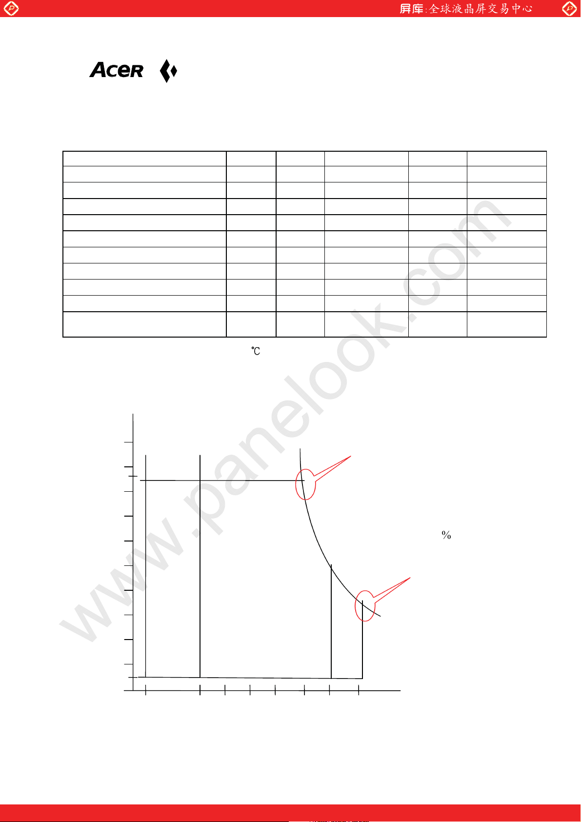
2.1 Display Characteristics
The following items are characteristics summary on the table under 25 ℃ condition:
www.panelook.com
ITEMS Unit SPECIFICATIONS
Screen Diagonal [mm] 338(13.3")
Active Area [mm] 270.336(H) x 202.752(V)
Pixels H x V 1024(x3) x 768
Pixel Pitch [mm] 0.264(per one triad) x 0.264
Pixel Arrangement R.G.B. Vertical Stripe
Display Mode Normally White
Typical White Luminance [cd/m2] 150
Contrast Ratio 200 : 1 Typ.
Optical Rise Time/Fall Time [msec] 30 Typ., 50 Max.
Nominal Input Voltage VDD [Volt] +3.3 V
Typical Power Consumption
(VDD line + VCFL line)
Weight [Grams] 450 Typ.
Physical Size [mm] 284(W) x 214.5(H) x 5.5(D)
Electrical Interface R/G/B Data, 3 Sync, Signals, Clock (4 pairs
Support Color Native 262K colors ( RGB 6-bit data driver )
Temperature Range
Operating
Storage (Shipping)
[Watt] 5.0(w/o Inverter, All black pattern)
LVDS)
o
C]
[
o
C]
[
0 to +50
-20 to +60
(C) Copyright Acer Display Technology, Inc.
October,2000 All Rights Reserved. L133x3-1 Ver.01 5/5
No Reproduction and Redistribution Allowed.
One step solution for LCD / PDP / OLED panel application: Datasheet, inventory and accessory!
www.panelook.com
Page 6
Global LCD Panel Exchange Center
gTyp
p
Display Technology
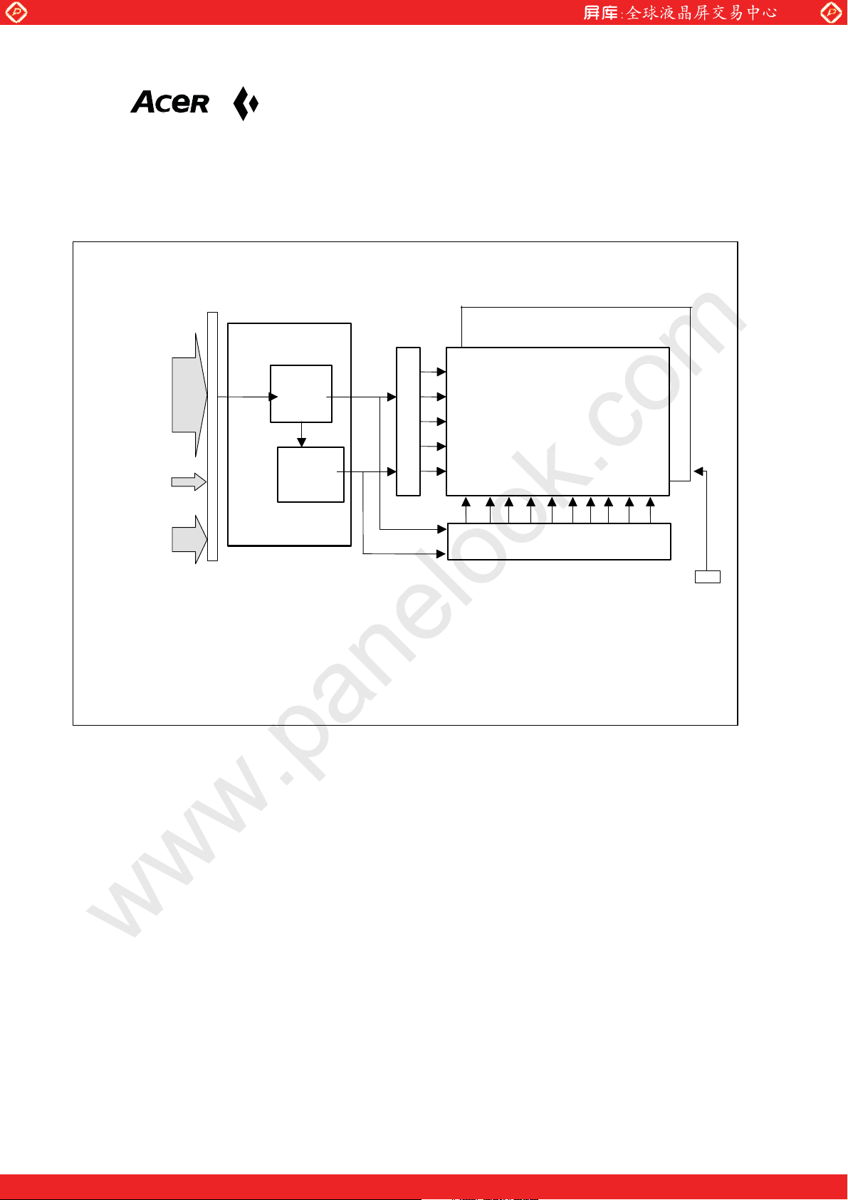
2.2 Functional Block Diagram
www.panelook.com
LCD DRIVE
CARD
6bit color data
for R/G/B
DSPTMG
Vsync
Hsync
(3 pairs LVDS)
DTCLK
(1 pairs LVDS)
VDD
GND
LCD
Controller
DC-DC
Converter
Ref circuit
LCD Connector
JAE JAE FI-AB20S-HF06
Mating Type JAE FI-A20M
Y-Driver
Backlight Unit
TFT
1024(R/G/B) x 3
X-Driver
Connector
Lam
JST BHSR-02VS-1
Matin
e SM02B-BHSS-1
(C) Copyright Acer Display Technology, Inc.
October,2000 All Rights Reserved. L133x3-1 Ver.01 6/6
No Reproduction and Redistribution Allowed.
One step solution for LCD / PDP / OLED panel application: Datasheet, inventory and accessory!
www.panelook.com
Page 7
Global LCD Panel Exchange Center
Display Technology
3.0 Absolute Maximum Ratings
Absolute maximum ratings of the module is as following:
Item Symbol Min Max Unit Conditions
Logic/LCD Drive Voltage VDD Vss-0.3 +4.0
Input Voltage of Signal Vin
CCFL Inrush current ICFLL - 20
CCFL Current ICFL - 7.5
Operating Temperature TOP 0 +50
Operating Humidity HOP 8 95
Storage Humidity HST 8 95
Storage Temperature TST -20 +60
Vibration 1.5 10-200
Shock 50 18
www.panelook.com
180 3
[Volt]
[Volt]
[mA]
[mA] rms
o
C]
[
[%RH]
[%RH]
o
[
C]
G Hz
G ms
G ms
Note 2
Note 1
Note 1
Note 1
Note 1
Rectangle wave
Half sine wave
Note 1 : Maximum Wet-Bulb should be 39Ċ and No condensation.
Note 2 : Duration=50 msec.
Wet bulb temperature chart
Relativive Humidity %
100
Twb=39
℃
T=40℃,H=95%
95
90
80
70
60
50
Storage range
40
Operation range
30
T=50℃,H=55%
T=60℃,H=39%
T=65℃,H=29%
20
Storage range
10
5
0
-20 0 6050
(C) Copyright Acer Display Technology, Inc.
October,2000 All Rights Reserved. L133x3-1 Ver.01 7/7
No Reproduction and Redistribution Allowed.
One step solution for LCD / PDP / OLED panel application: Datasheet, inventory and accessory!
Temperature
o
C
www.panelook.com
Page 8

Global LCD Panel Exchange Center
Display Technology
4.0 Optical Characteristics
The optical characteristics are measured under stable conditions as follows under 25℃ condition:
Item Conditions Min. Typ. Max.
Viewing Angle
K: Contrast Ratio
Contrast ratio
Response Time
Color / Chromaticity Red x
Coordinates (CIE) Red y
White Luminance
CCFL 6mA
www.panelook.com
[degree]
[degree]
[degree]
[degree]
[msec]
[msec]
[cd/m
Horizontal (Right)
K = 10 (Left)
Vertical (Upper)
K = 10 (Lower)
Rising
Falling
Green x
Green y
Blue x
Blue y
White x
White y
2
] 120 150
40
40
10
30
0.537 0.577 0.617
0.308 0.338 0.368
0.280 0.310 0.340
0.533 0.563 0.593
0.128 0.158 0.188
0.117 0.157 0.197
0.283 0.313 0.343
0.299 0.329 0.359
20
35
200
20 30
30 50
(C) Copyright Acer Display Technology, Inc.
October,2000 All Rights Reserved. L133x3-1 Ver.01 8/8
No Reproduction and Redistribution Allowed.
One step solution for LCD / PDP / OLED panel application: Datasheet, inventory and accessory!
www.panelook.com
Page 9

Global LCD Panel Exchange Center
Display Technology
5.0 Signal Interface
5.1 Connectors
Physical interface is described as for the connector on module.
These connectors are capable of accommodating the following signals and will be following components.
www.panelook.com
Manufacturer
Type / Part Number
5.2 Signal Pin
Fr inl
JAE
FI-AB20S-HF06
FI-A20H
JST
BHSR-02VS-1
SM02B-BHSS-1
Pin# Signal Name Pin# Signal Name
1 VDD 2 VDD
3 GND 4 GND
5 Rxin0- 6 Rxin0+
7 GND 8 Rxin1-
9 Rxin1+ 10 GND
11 Rxin2- 12 Rxin2+
13 GND 14 Rxclk15 Rxclk+ 16 GND
17 NC 18 Reserved
19 GND 20 GND
nn
r
(C) Copyright Acer Display Technology, Inc.
October,2000 All Rights Reserved. L133x3-1 Ver.01 9/9
No Reproduction and Redistribution Allowed.
One step solution for LCD / PDP / OLED panel application: Datasheet, inventory and accessory!
www.panelook.com
Page 10

Global LCD Panel Exchange Center
Display Technology
5.3 Signal Description
The module using a LVDS receiver SN75LVDS86DGG(Texas Instruments) or compatible. LVDS is a
differential signal technology for LCD interface and high speed data transfer device. Transmitter shall be
SN75LVDS84DGG(negative edge sampling) or compatible.
Pin# Signal Name Description
1 VDD +3.3V Power Supply
2 VDD +3.3V Power Supply
3 GND Ground
4 GND Ground
5 Rxin0- Negative LVDS differential data input (R0-R5, G0)
6 Rxin0+ Positive LVDS differential data input (R0-R5, G0)
7 GND Ground
8 Rxin1- Negative LVDS differential data input (G1-G5, B0-B1)
9 Rxin1+ Positive LVDS differential data input (G1-G5, B0-B1)
10 GND Ground
11 Rxin2- Negative LVDS differential data input (B2-B5,
12 Rxin2+ Positive LVDS differential data input (B2-B5,
13 GND Ground
14 Rxclk- Negative LVDS differential clock input
15 Rxclk+ Positive LVDS differential clock input
16 GND Ground
17 NC Reserved for future use
18 Reserved Reserved for LVDS MFG test
www.panelook.com
HSYNC,VSYNC,DSPTMG)
HSYNC,VSYNC,DSPTMG)
19 GND Ground
20 GND Ground
Internal circuit of LVDS inputs are as following.
(C) Copyright Acer Display Technology, Inc.
October,2000 All Rights Reserved. L133x3-1 Ver.01 10/10
No Reproduction and Redistribution Allowed.
One step solution for LCD / PDP / OLED panel application: Datasheet, inventory and accessory!
www.panelook.com
Page 11

Global LCD Panel Exchange Center
Display Technology
Signal Input
Pin No.
5
Rxin0-
6
Rxin0+
8
Rxin1-
www.panelook.com
SN75LVDS86DGG or Compatible
9
Rxin1+
11
Rxin2-
12
Rxin2+
14
Rxclk-
15
Rxclk+
The module uses a 100 ohm resistor between positive and negative data lines of each receiver input.
Signal
Description
Name
+RED5
+RED4
+RED3
+RED2
+RED1
+RED0
Red Data 5 (MSB)
Red Data 4
Red Data 3
Red Data 2
Red Data 1
Red Data 0 (LSB)
Each red pixel's brightness data consists of these 6 bits pixel data.
Red-pixel Data
+GREEN 5
+GREEN 4
(C) Copyright Acer Display Technology, Inc.
October,2000 All Rights Reserved. L133x3-1 Ver.01 11/11
No Reproduction and Redistribution Allowed.
Green Data 5 (MSB)
Green Data 4
One step solution for LCD / PDP / OLED panel application: Datasheet, inventory and accessory!
www.panelook.com
Page 12

Global LCD Panel Exchange Center
)
Display Technology
www.panelook.com
+GREEN 3
+GREEN 2
+GREEN 1
+GREEN 0
+BLUE 5
+BLUE 4
+BLUE 3
+BLUE 2
+BLUE 1
+BLUE 0
-DTCLK
DSPTMG
VSYNC
HSYNC
Note: Output signals from any system shall be low or Hi-Z state when VDD is off.
Green Data 3
Green Data 2
Green Data 1
Green Data 0 (LSB)
Green-pixel Data
Blue Data 5 (MSB)
Blue Data 4
Blue Data 3
Blue Data 2
Blue Data 1
Blue Data 0 (LSB)
Blue-pixel Data
Data Clock
Display Timing
Vertical Sync
Horizontal Sync
Each green pixel's brightness data consists of these 6 bits pixel data.
Each blue pixel's brightness data consists of these 6 bits pixel data.
The typical frequency is 65.0 MHz. The signal is used to strobe the pixel
data and DSPTMG signals. All pixel data shall be valid at the falling
edge when the DSPTMG signal is high.
This signal is strobed at the falling edge of -DTCLK. When the signal is
high, the pixel data shall be valid to be displayed.
The signal is synchronized to -DTCLK .
The signal is synchronized to -DTCLK .
5.4 Signal Electrical Characteristics
Each signal characteristics are as follows;
Parameter Condition Min Max Unit
Differential Input
Vth
Vtl
Note: It is recommended to refer the specifications to SN75LVDS86DGG (Texas Instruments) in detail.
High
Voltage(Vcm=+1.2V)
Differential Input Low
Voltage(Vcm=+1.2V
100
-100
[mV]
[mV]
(C) Copyright Acer Display Technology, Inc.
October,2000 All Rights Reserved. L133x3-1 Ver.01 12/12
No Reproduction and Redistribution Allowed.
One step solution for LCD / PDP / OLED panel application: Datasheet, inventory and accessory!
www.panelook.com
Page 13

Global LCD Panel Exchange Center
Display Technology
6.0 Pixel format image
Following figure shows the relationship of the input signals and LCD pixel format.
0 1 1022 1023
www.panelook.com
1st Line
768th Line
R G B R G B
R G B R G B
R G B R G B
R G B R G B
(C) Copyright Acer Display Technology, Inc.
October,2000 All Rights Reserved. L133x3-1 Ver.01 13/13
No Reproduction and Redistribution Allowed.
One step solution for LCD / PDP / OLED panel application: Datasheet, inventory and accessory!
www.panelook.com
Page 14
Global LCD Panel Exchange Center
s
Display Technology
7.0 Backlight Characteristics
7.1 Signal for Lamp connector
1 Lamp High Voltage
www.panelook.com
2
Lamp Low Voltage
7.2 Parameter guide line for CFL Inverter
Symbol Parameter Min D.P
Note 1
(L63) White Luminance 120 150 -
ICFL CCFL current 2.0 6.0 7.5
ICFLL CCFL Inrush current - - 20
fCFL CCFL Frequency 40 50 60
ViCFL CCFL Ignition Voltage
VCFL CCFL Discharge Voltage
(Reference)
PCFL CCFL Power consumption 3.6
601
Max Units Condition
[cd/m
[mA]
rm
[mA]
[KHz] (Ta=25℃)
1220 [Volt]
rms
[Volt]
rms
[Watt] (Ta=25℃)
2
] (Ta=25℃)
(Ta=25℃)
Note 2
Note 3
(Ta= 0℃)
Note 5
(Ta=25℃)
Note 4
Note 4
Note 1: Design Point-2 ; At White Luminance 150 cd/m2, PCFL=3.6W is required.
Note 2: Duration=50 [msec]
Note 3: CCFL Frequency should be carefully determined to avoid interference between inverter and TFT LCD
Note 4: Calculator value for reference (ICFL×VCFL=PCFL)
Note 5: CCFL inverter should be able to give out a power that has a generating capacity of over 880 voltage.
Lamp units need 880 voltage minimum for ignition.
(C) Copyright Acer Display Technology, Inc.
October,2000 All Rights Reserved. L133x3-1 Ver.01 14/14
No Reproduction and Redistribution Allowed.
One step solution for LCD / PDP / OLED panel application: Datasheet, inventory and accessory!
www.panelook.com
Page 15

Global LCD Panel Exchange Center
Display Technology
8.0 Interface Timings
Basically, interface timings described here is not actual input timing of LCD module but output timing of
SN75LVDS86DGG (Texas Instruments) or equivalent.
8.1 Timing Characteristics
Symbol Description Min Typ Max Unit
fdck DTCLK Frequency 65.00 [MHz]
tck DTCLK cycle time 15.38 [nsec]
tx X total time 1206 1344 2047 [tck]
tacx X active time 129 1024 [tck]
tbkx X blank time 90 320 [tck]
Hsync H frequency 48.363 [KHz]
Hsw H-Sync width 2 136 [tck]
Hbp H back porch 1 160 [tck]
Hfp H front porch 0 24 [tck]
ty Y total time 771 806 1023 [tx]
tacy Y active time 768 [tx]
Vsync Frame rate (55) 60 61 [Hz]
Vw V-sync Width 2 6 [tx]
Vfp V-sync front porch 1 3 [tx]
Vbp V-sync back porch 7 29 63 [tx]
www.panelook.com
Note: Hsw(H-sync width) + Hbp(H-sync back porch) should be less than 515 tck.
8.2 Timing Definition
(C) Copyright Acer Display Technology, Inc.
October,2000 All Rights Reserved. L133x3-1 Ver.01 15/15
No Reproduction and Redistribution Allowed.
One step solution for LCD / PDP / OLED panel application: Datasheet, inventory and accessory!
www.panelook.com
Page 16

Global LCD Panel Exchange Center
x
x
Display Technology
www.panelook.com
tx
H-Sync
DSPTM
V-Sync
DSPTM
3t
Hsw
6t
38tx
HbpHfp
tacx
29tx
768tx
(C) Copyright Acer Display Technology, Inc.
October,2000 All Rights Reserved. L133x3-1 Ver.01 16/16
No Reproduction and Redistribution Allowed.
One step solution for LCD / PDP / OLED panel application: Datasheet, inventory and accessory!
www.panelook.com
Page 17

Global LCD Panel Exchange Center
Display Technology
9.0 Power Consumption
Input power specifications are as follows;
Symble Parameter Min Typ Max Units Condition
VDD Logic/LCD Drive
Voltage
PDD VDD Power 1.2 1.3 [Watt] All Black Pattern
PDDmax VDD Power max 1.60 [Watt] Sub-pixel checker
VDDrp Allowable
Logic/LCD Drive
Ripple Voltage
VDDns Allowable
Logic/LCD Drive
Ripple Noise
www.panelook.com
3.0 3.3 3.6 [Volt] Load Capacitance 100uF typ.
100 [mV]
p-p
100 [mV]
p-p
(C) Copyright Acer Display Technology, Inc.
October,2000 All Rights Reserved. L133x3-1 Ver.01 17/17
No Reproduction and Redistribution Allowed.
One step solution for LCD / PDP / OLED panel application: Datasheet, inventory and accessory!
www.panelook.com
Page 18

Global LCD Panel Exchange Center
Display Technology
10. Power ON/OFF Sequence
VDD power and lamp on/off sequence is as follows. Interface signals are also shown in the chart. Signals
from any system shall be Hi-Z state or low level when VDD is off.
www.panelook.com
10ms min.
VDD
10%
0 V
Signals
0 V
Lamp On
0 V
90%
30ms max.
0 min. 0 min.
10% 10%
170ms min. 0 min.
10% 10%
90%
10% 10%
(C) Copyright Acer Display Technology, Inc.
October,2000 All Rights Reserved. L133x3-1 Ver.01 18/18
No Reproduction and Redistribution Allowed.
One step solution for LCD / PDP / OLED panel application: Datasheet, inventory and accessory!
www.panelook.com
Page 19

Global LCD Panel Exchange Center
Display Technology
11.0 Packing dimension
Module weight : less than 480 gm.
Carton dimension: The outside dimension of carton is 390 L mm x 360 Wmm x 455 Hmm
Shipping Weight: less than 8.5 Kg for each carton.
www.panelook.com
UPPER
LABEL
TOP CUSHION
LCD MODULE
BOTTOM
CUSHION
CARTON
(C) Copyright Acer Display Technology, Inc.
October,2000 All Rights Reserved. L133x3-1 Ver.01 19/19
No Reproduction and Redistribution Allowed.
One step solution for LCD / PDP / OLED panel application: Datasheet, inventory and accessory!
www.panelook.com
Page 20

Global LCD Panel Exchange Center
www.panelook.com
One step solution for LCD / PDP / OLED panel application: Datasheet, inventory and accessory!
www.panelook.com
Page 21

Global LCD Panel Exchange Center
www.panelook.com
Display Technology
One step solution for LCD / PDP / OLED panel application: Datasheet, inventory and accessory!
(C) Copyright Acer Display Technology, Inc.
October,2000 All Rights Reserved. L133x3-1 Ver.01 21/21
No Reproduction and Redistribution Allowed.
www.panelook.com
Page 22

Global LCD Panel Exchange Center
www.panelook.com
Display Technology
UL
X X / X X
MADE IN TAIWAN
(C) Copyright Acer Display Technology, Inc.
October,2000 All Rights Reserved. L133x3-1 Ver.01 22/22
No Reproduction and Redistribution Allowed.
One step solution for LCD / PDP / OLED panel application: Datasheet, inventory and accessory!
www.panelook.com
 Loading...