

Page 1

Diamond View Monitor
1786FD2
Service Guide
July 2002
Distributed by
Mitsubishi Electric Australia Pty.Ltd.
A.B.N. 58 001 215 792
348 Victoria Road
RYDALMERE NSW 2116
Australia
Telephone 1300 605 808
Page 2

Copyright
Copyright ã 1996 by the Company. All rights reserved. No part of this publication may be
reproduced, transmitted, transcribed, stored in a retrieval system, or translated into any language or
computer language, in any form or by any means, electronic, mechanical, magnetic, optical,
chemical, manual or otherwise, without the prior written permission of the Company.
Disclaimer
The Company makes no representations or warranties, either expressed or implied, with respect to
the contents hereof and specifically disclaims any warranties, merchantability or fitness for any
particular purpose. Further, the Company reserves the right to reserve this publication and to make
changes from time to time in the contents hereof without obligation of the Company to notify any
person of such revision or changes.
ii
Page 3

Section
Diamond View 1786FD2
Manual Contents
1. Engineering Specifications
2. Circuit Operation Theory
3. Alignment procedure
4. Trouble Shooting
5. Schematic Diagrams
Page 4

MEA 1786FD2 CRT Monitor Service Guide
Engineering Specification
Table of Contents
0. INTRODUCTION :......................................................................................................................................3
1. ELECTRICAL CHARACTERISTICS......................................................................................................3
1.1 POWER SUPPLY....................................................................................................................................3
1.2SIGNALINTERFACE ..............................................................................................................................3
1.3 SCAN RANGE.........................................................................................................................................3
1.4
VIDEO PERFORMANCE ........................................................................................................................4
1.5 TIMINGS .................................................................................................................................................4
2.ENVIRONMENT & RELIABILITY..........................................................................................................5
3.CRT CHARACTERISTICS.........................................................................................................................6
4.FRONT OF SCREEN...................................................................................................................................6
4.1 GEOMETRY............................................................................................................................................6
4.2SHARPNESS CRISPNESS ......................................................................................................................7
4.3 LIGHT QUALITY ...................................................................................................................................7
4.4 IMAGE STABILITY...............................................................................................................................7
5. USER CONTROLS......................................................................................................................................8
5.1 BASIC......................................................................................................................................................8
5.2 ADVANCED............................................................................................................................................8
6. MECHANICAL CHARACTERISTICS....................................................................................................9
6.1 DIMENSION............................................................................................................................................9
6.2 WEIGHT..................................................................................................................................................9
6.3 PLASTIC..................................................................................................................................................9
6.4 CARTON..................................................................................................................................................9
7. PALLET & SHIPMENT ...........................................................................................................................10
7.1 DIMENSION..............................................................................................................................................10
7.2 SHIPPING CONTAINER..............................................................................................................................10
7.3 AIR TRANSPORT CONTAINER...................................................................................................................11
8. CERTIFICATION .....................................................................................................................................11
9. APPENDIX TABLE...................................................................................................................................13
TABLE 1 - DDC TABLE...............................................................................................................................13
1
Page 5

MEA 1786FD2 CRT Monitor Service Guide
Engineering Specification
Table of Contents
TABLE 2 - CRT BLEMISH & SCRATCH SPEC......................................................................................25
TABLE 3 - OSD MENU.................................................................................................................................25
TABLE 4 - GEOMETRY FIG......................................................................................................................26
TABLE 5 - TCO 99 SPEC.............................................................................................................................40
2
Page 6
MEA 1786FD2 CRT Monitor Service Guide
Engineering Specification
0. Introduction :
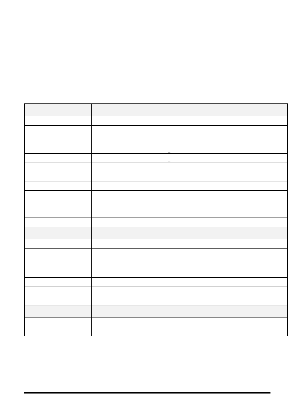
The subject model is designed for a value line 17” color monitor. It has the following figures :
0.25mm dot pitch CRT, 135MHz video bandwidth, 1280x1024 max. resolution.
Low radiation TCO99 standard.
ISO 14000 certificated green design. (Refer Table 5)
1. Electrical Characteristics
1.1 POWER SUPPLY
Voltage Universal input full range 90~264VAC /47~63Hz
Input Current 90 ~ 264VAC 2.0 Arms
Power consumption On < 100 W max
DPMS Standby < 5 W
Suspend < 5 W
Off < 5 W
Condition Spec
OK
N.A
√
√
√
√
√
√
LED : Green
LED : Amber
LED : Amber
LED : Amber
Remark
Inrush Current 110 VAC/50Hz 40 Amp peak
Leakage Current 264 VAC/50Hz < 3.5mA
Hi-Pot 1. 1500VAC, 1 sec
2. Ground test : 30A,
1sec
Power cord Length : 1800 mm Color : Flint Gray
1.2SIGNALINTERFACE
Pin assignment 5V on Pin 9
Video input Level / Impedance 700mV / 75 Ohm
Sync input TTL-Positive/Negative
Impedance 50 Ohm on H-sync cable
Signal Cable D-Sub 1.5M +/- 20mm
BNC
Color Flint Gray
Condition
1.3 SCAN RANGE
w/o damage
< 0.1 ohm
Spec
Spec
√
√
√
√
OK
N.A
√
√
√
√
√
√
√
OK
N.A
cold-start
(in-line test)
(in-lab test)
KC-003
Remark
0.7μs<H-sync width<25% of H period
2μs<V-sync width< 400μs
Remark
Horizontal 31 ~ 86 KHz
Vertical 50~ 120 Hz
3
√
√
Page 7
MEA 1786FD2 CRT Monitor Service Guide
Engineering Specification
VIDEO
1.4
Condition Spec
OK
N.A
Remark
PERFORMANCE
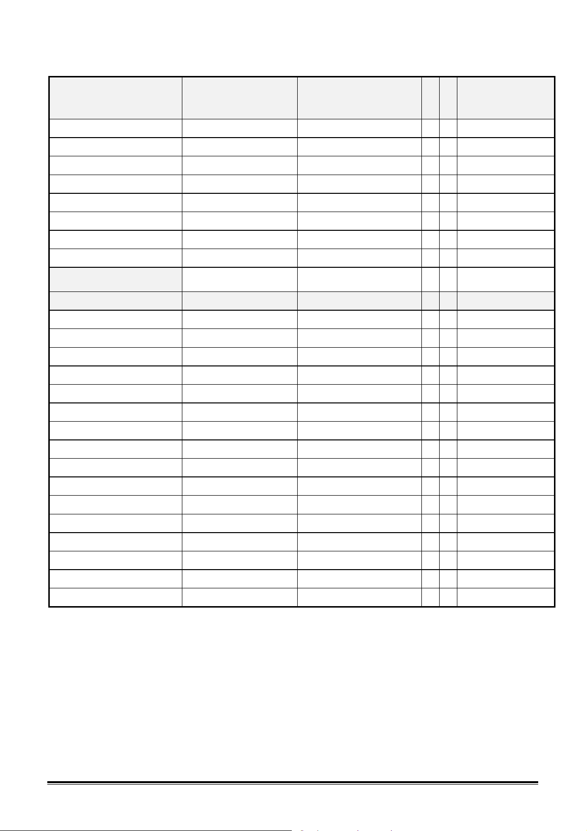
Dot Rate 135 MHz
Max. Resolution 1280 x 1024
Rise time/Fall time 5.5 ns
Video Ringing 5% max
Sag 5% max
Bandwidth -3db 135 MHz
DDC Version DDC1/2B
EDID Ver 2 ,Rev 1, Ver 3
1.5 TIMINGS
Preset
VGA400 640x400 31.47KHz/70Hz
Preset mode No. : 6 User mode No. : 10
Resolution Fh (KHz) / Fv (Hz)
√
√
√
√
√
√
√ see table 1
√
OK
N.A
√
Remark
VGA480 640x480 31.47KHz/59.94Hz
6448A 640X480 37.5KHz/75Hz
6448B
SVGA4 800x600 46.88KHz/75Hz
SVGA3 800x600 48.09KHz/72.01Hz
SVGA5 800x600 53.67KHz/85Hz
Apple 16” 832x624 49.71KHz/74.533Hz
UVGA2 1024x768 56.476KHz/70.069Hz
UVGA7 1024x768 60.023KHz/75.029Hz
Super MAC 19 1024x768 60.24KHz/75Hz
UVGA8 1024x768 68.68KHz/85Hz
VESA-XGA 1280x1024 63.981KHz/60.020Hz
WS7 1280x1024 79.98KHz/75Hz
WS8 1280x1024 91.15KHz/85Hz
VESA1600 1600x1200 93.75KHz/75Hz
640X480 43.269KHz/85Hz
√
√
√
√
√
√
√
√
√
√
√
√
√
√
√
4
Page 8
MEA 1786FD2 CRT Monitor Service Guide
Engineering Specification
2.Environment & Reliability
Condition Spec
O
K
N.A
Remark
2
/Hz
√
Non-condensing
√
Non-condensing
√
Without packing
√
With packing
√
√
√
√
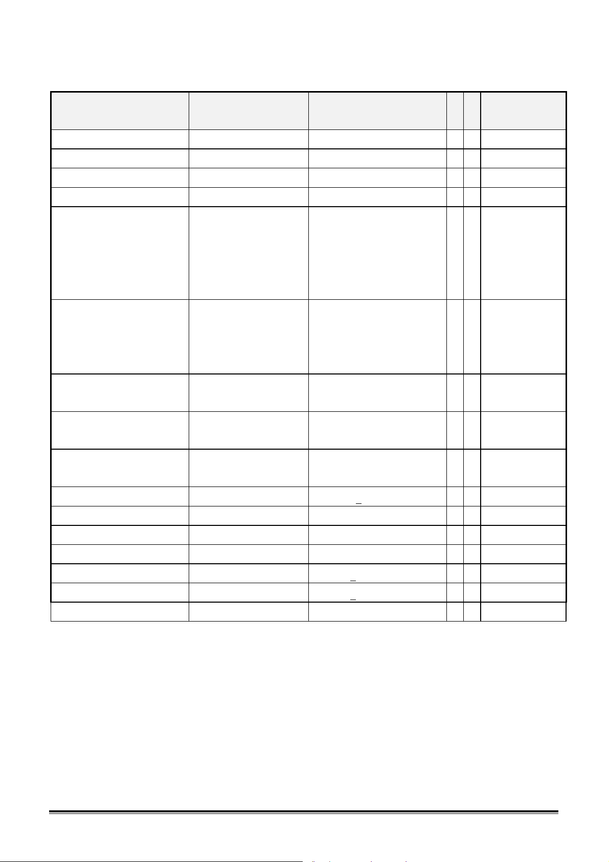
Operation Temp./Humidity +5 ~ +40℃/ 20~90% R.H.
Non- Operation Temp./Humi. -20~ +60℃/ 10~90% R.H.
Altitude Operating condition 0~3048m (10,000ft)
Non-operating condition 0~12,192m (40,000ft)
Vibration
1)Sine Wave Vibration Package, Non-Operating 5 ~ 26.6Hz /0.6g
26.6 ~ 50Hz /0.016”
50~500Hz/ 2.0g
(104 Minutes/Axis for x, y, z)
2)Random Vibration
Non-package,
Drop (With packing) Package, Non-Operating 19.4kg - 61cm Height
Package, Non-Operating 5 ~ 100Hz, 0 dB/Oct.
2
0.015g
100 ~ 200Hz, -6 dB/Oct., ----200Hz, ------ , 0.0038g
Non-Operating
/Hz
20Hz~2000/ 0.0185g2/Hz
1 corner, 3 edges, 6 faces.
Electrostatic Discharge
Acoustical Noise < 40 dB/A
Power Line Transient
IEC1000-4-5 (Surge)
MTBF Demonstration 90% confidence level > 60,000 Hrs
MTBF Prediction
IEC801-4,IEC1000-4-4 Coupling clamp 0 ~ 4KV
MIL-217F
IEC801-2 standard Contact:8KV, Air:15KV
Common:2KV,Differential:1KV
IEC1000-4-12 (100KHz ringwave)
Common:3KV,Differential:1KV
> 40,000 Hrs
CRT Life 78% degradation > 10000 Hrs
√
√
√
√
√
√
√
0.5~8KV tip table no
blanking
Excluding the CRT
Excluding the CRT
√
5
Page 9
MEA 1786FD2 CRT Monitor Service Guide
Engineering Specification
3.CRT Characteristics
Spec
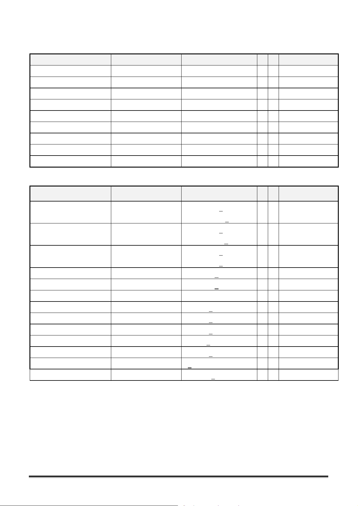
CRT Vender SAMSUNG
Technology FST
Coating Anti-reflection/Anti-static
Dot pitch 0.25mm
Phosphor P22
Light transmittance 52.6%
Viewable size 16”
Deflection angle 90 deg
Blemishes and scratches
1 trio missing, as approval sheet
OK
N.A
√
√
√
√
√
√
√
√
√ see table 2
Remark
4.Front of Screen
4.1 GEOMETRY
OK
N.A
Remark
Magnetic Environment Northern Hemisphere H = 0 + 0.05
V = +0.45 +
Southern Hemisphere H = 0 + 0.05
V = -0.45 +
Equatorial H = 0 + 0.05
V = 0 +
Size Hor. 310 + 4 mm
Ver. 230 + 4 mm
Centering Hor. & Ver. |A-B|,|C-D|< 4 mm
Geometric Distortion
Hor./Ver. Trapezoid < 2 mm
Orthogonal < 2 mm
S-curve < 0.5 mm within 40mm
Linearity Hor. & Ver. < 5 %
Top/Bottom / Side Pincushion
Top/Bottom / Side Barreling
Tilt <
< 2 mm
< 2 mm
1.2 mm
0.05
0.05
0.05
√
√
√
√
√
√ See table 4
√
See table 5 for TCO99
√ “
√
√
√
√
√
(Xmax-Xmin)/( Xmax+Xmin)*100
6
Page 10
MEA 1786FD2 CRT Monitor Service Guide
Engineering Specification
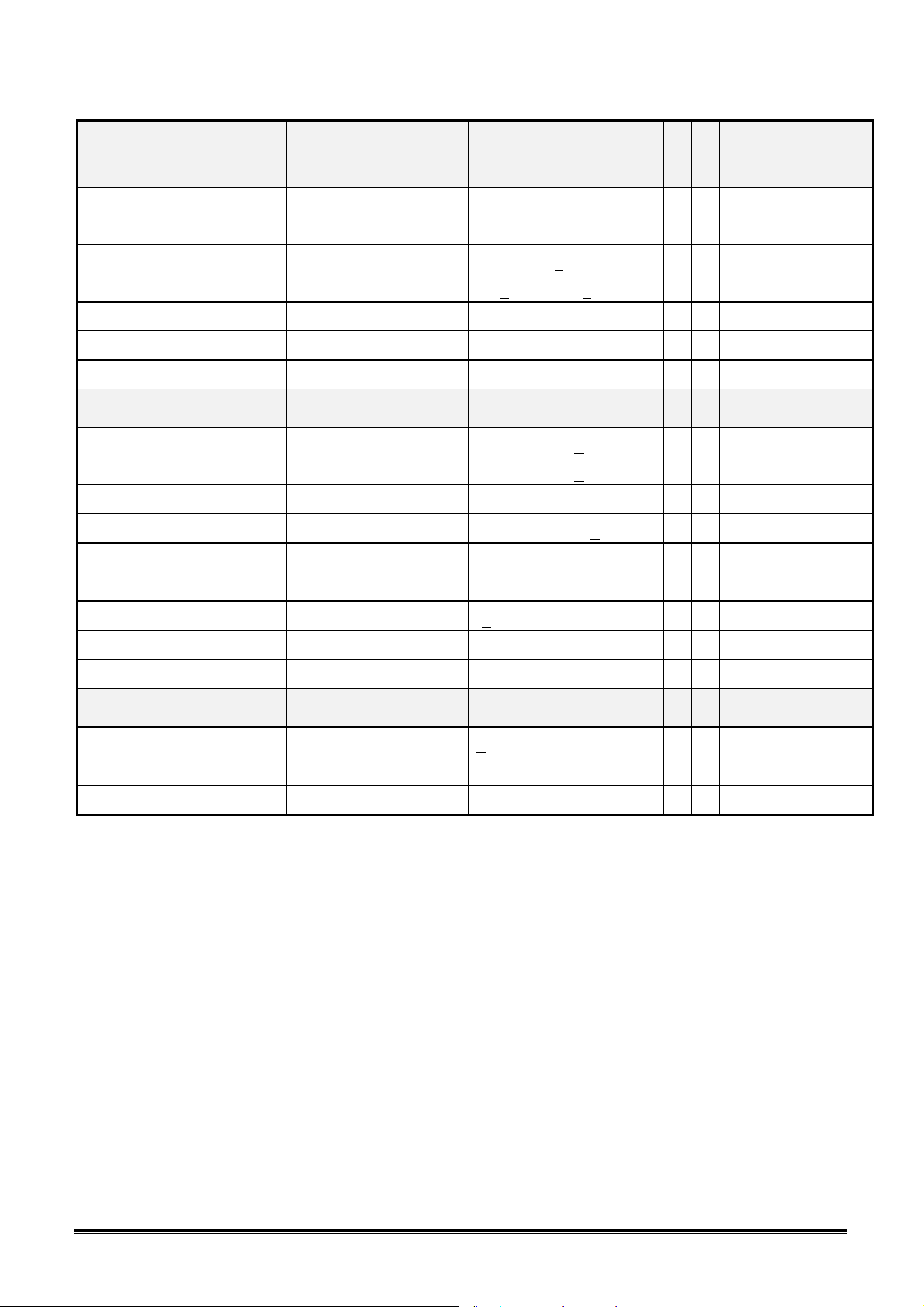
4.2SHARPNESS
OK
N.A
Remark
CRISPNESS
Focus
Mis-convergence Center < 0.15 mm
Moire Over 25Ft-L no visible moire
Swing not permitted
Reverse character(white
background and black characters)
“e,w,m” at cut-off and
1024 x 768 resolution
A <
0.25mm ,B< 0.35mm
Jitter < 2mm
4.3 LIGHT QUALITY
White Balance Full white center
(Brit. cut-off & Cont. max.)
Purity W,R,G,B
X max-X min & Y max-Y min
Condition Spec
x = 0.283 +
y = 0.297 +
< 0.015
0.010
0.010
√
√
√
√
”
The distance of watch is
30cm from eyes to screen
√ ”
OK
N.A
√
√
Remark
@ UVGA8 1024x768
68.68KHz/85Hz
”
Color Tracking
Max Brightness with ABL
Max Brightness no ABL
Brightness Uniformity
Raster light O/P
Contrast ratio
4.4 IMAGE STABILITY
Brightness cut off
Full white pattern
3” Block
Full white pattern
Bright max./Cont. min.
Max/Min
> 70% (center to corner)
x, y (nominal) + 0.015
28Ft-L min.(Cut-off)
40Ft-L min.(Cut-off)
0.5 ~ 1.5Ft-L
5:1
H/V regulation < 1 mm per side at cut-off
Flicker No flicker
Ringing
Video at center
No visible DY Hor. Video ringing
√ ”
√
”
√ ”
√
”
√ ”
√ ”
OK
N.A
Remark
√
√
√
7
Page 11
MEA 1786FD2 CRT Monitor Service Guide
Engineering Specification
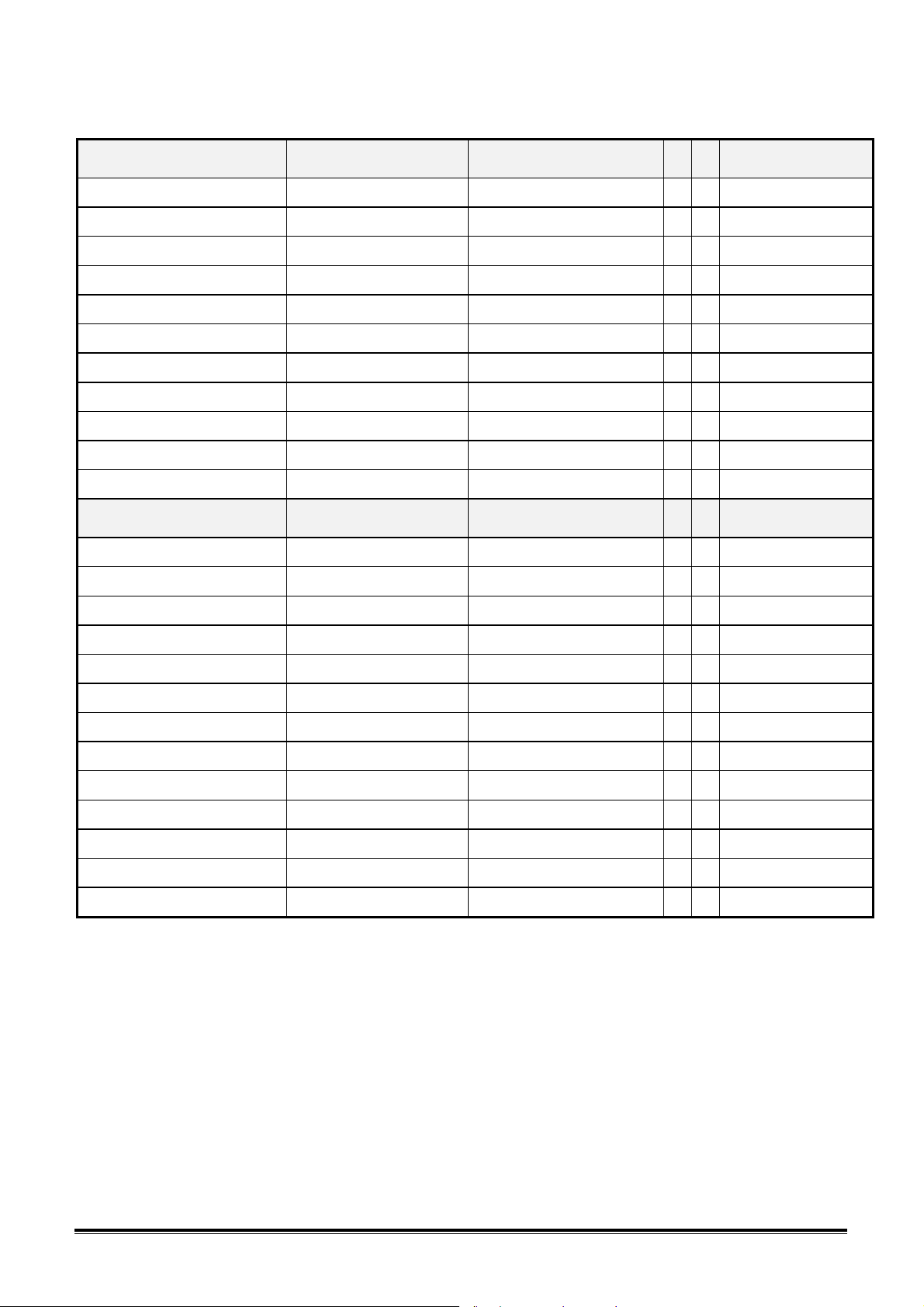
5. User Controls
5.1 BASIC
Function Spec
Power Switch
Contrast
Brightness
H Size
H Position
V Size
V Position
Barrel/Pincushion
Parallelogram
Trapezoid
I-Key
5.2 ADVANCED
Function Spec
OK
N.A
√
√
√
√
√
√
√
√
√
√
√
OK
N.A
Remark
Remark
OSD position
Color Gain
Corner
Pin-balance
Tilt
Color Temp. C1, C2
9300K, 6500K
Manual Degauss
Recall
Languages 5 languages
Mis-convergence adj.
Moire adj.
D-sub/BNC switch
√
See Table 3
√
√
√
√
√
√
√
√
√
√
√
8
Page 12
MEA 1786FD2 CRT Monitor Service Guide
Engineering Specification
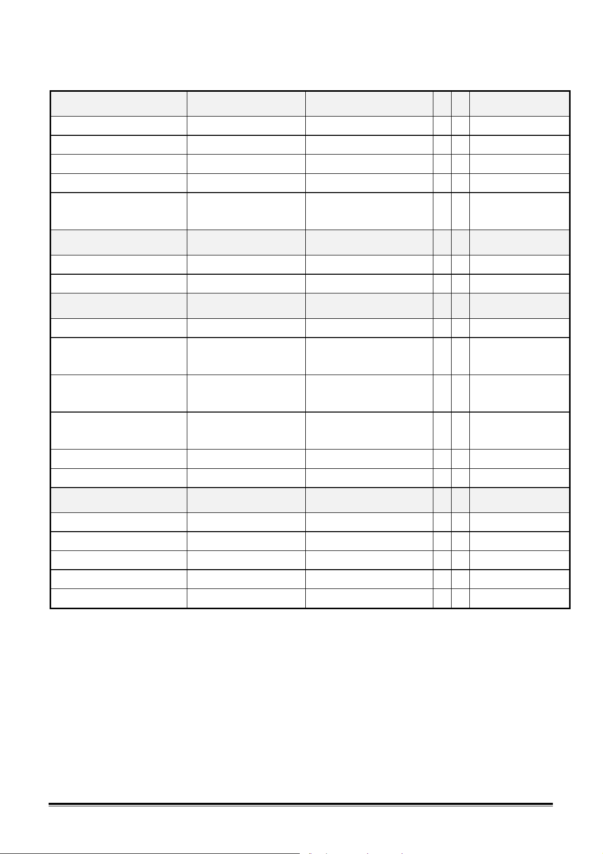
6. Mechanical Characteristics
6.1 DIMENSION
Bezel opening 324.8 x 243.5 mm
Monitor w/o Stand L x W x H mm 417.5x406x371 mm
Monitor w Stand L x W x H mm 417.5x406x422 mm
Carton Box (outside) L x W x H mm 575x540x470 mm
Tilt and Swivel range Tilt : -4/+12 degree
6.2 WEIGHT
Monitor (Net) 16.4 Kg
Monitor w packaging(Gross) 19.4 Kg
6.3 PLASTIC
Flammability UL 94-V0
Spec
Swivel:- 45/ +45 degrees
Spec
Spec
OK
N.A
√
√
√
√
√
OK
N.A
√
√
OK
N.A
√
Remark
Remark
Remark
Heat deflection To ABS
PC + ABS
UV stability ABS
PC + ABS
Resin MPR2 : ABS
Texture RE-6625
Color Light Gray
6.4 CARTON
Color Kraft
Material A B Flute
Compression strength 530 KGF
Burst Strength 23 KGF/cm2
Stacked quantity 5 Layers
Spec
Delta E< 5 after 300Hr Xted test
Delta E< 1.5 after 300Hr Xted test
65 ℃
70 ℃
TCO : PC + ABS
√
√
MPR2 Model
TCO Model
√
√
√
OK
N.A
Remark
√
√
√
√
√
9
Page 13
MEA 1786FD2 CRT Monitor Service Guide
Engineering Specification
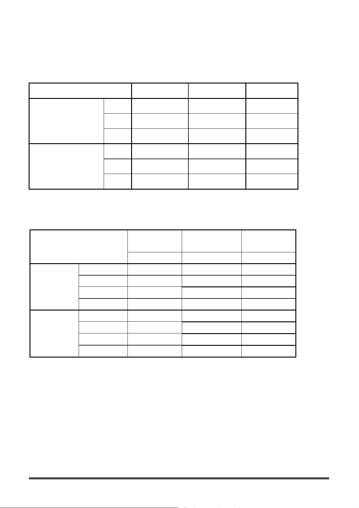
7. Pallet & Shipment
7.1 Dimension
Transport Type Pallet A Pallet B Pallet C
Shipping Pallet Length 1150 X X
Dimension(mm) Width 1080 X X
Height 120 X X
Air Transport Pallet Length 1150 1725 X
Dimension(mm) Width 1080 1080 X
Height 120 120 X
7.2 Shipping Container
Stowing Type Quantity of products
(Every container) (Every Pallet) (Every Container)
20' 160 Pallet A: 16 Pallet A: 10
Pallet B: X Pallet B: X
With pallet 40' 352 Pallet A: 16 Pallet A: 22
Pallet B: X Pallet B: X
20' 160 X X
X X
Without pallet 40' 440 X X
X X
(sets)
Quantity of Products
(sets)
Quantity of pallet
(sets)
10
Page 14
MEA 1786FD2 CRT Monitor Service Guide
Engineering Specification
7.3 Air Transport Container
Container Type Quantity of products
(sets)
(Every container)
Container
3048 * 2286 * 2438
Pallet B: 24 Pallet B: 2
80
Quantity of Products
(sets)
(Every Pallet)
Pallet A: 16 Pallet A: 2
Quantity of pallet
(sets)
(Every Container)
8. Certification
Condition Spec
Environment Green design API Doc. 715-C49
OK
N.A
√
Remark
ISO14000 Requirement
Blue Angel German Standard
E-2000 Switzerland
NUTEK Swedish Standard
EPA USA Standard
EN61000-3-2 Harmonics
TCO92/95
TCO99
PC-Monitor Microsoft Windows PC98/99
DPMS VESA
DDC 1/2B Version 3.0
USB External
Safety UL (USA) UL 1950 3rd edition
CSA (Canada) C22.2 No. 950-M95
DNSF EN60950
IEC950 +A1+A2+A3+A4
EN60950 +A1+A2+A3+A4
√
√
√
√
√
√
√
√
√
√
√
√
√
√
√
√
73/23/EEC
√
11
Page 15
MEA 1786FD2 CRT Monitor Service Guide
Engineering Specification
CB (Nordics)
TUV/GS EN60950
CCEE (China)
EIAJ/JEIDA (Japan)
NOM (Mexico)
IAA (Korea)
EMC CE Mark 89/336/EEC
FCC (USA) Class B
EN55022 Class B
CISPR 22 Class B
VCCI (Japan) Class B
BSMI (Taiwan)
C-Tick (Australia) AS3548
RRL (Korean)
√
√
√
√
√
√
√
√
√
√
√
√
√
√
X- Ray Requirement DHHS (21 CFR) USA X- Ray Standard
DNHW
PTB German X- Ray standard
MPRII(EN50279)
MPRIII
Ergonomics 2 PfG 1041/1299 German ergonomic
ISO 9241-3 -7 & 8
√
√
√
√
√
√
√
12
Page 16
MEA 1786FD2 CRT Monitor Service Guide
Engineering Specification
9. Appendix Table
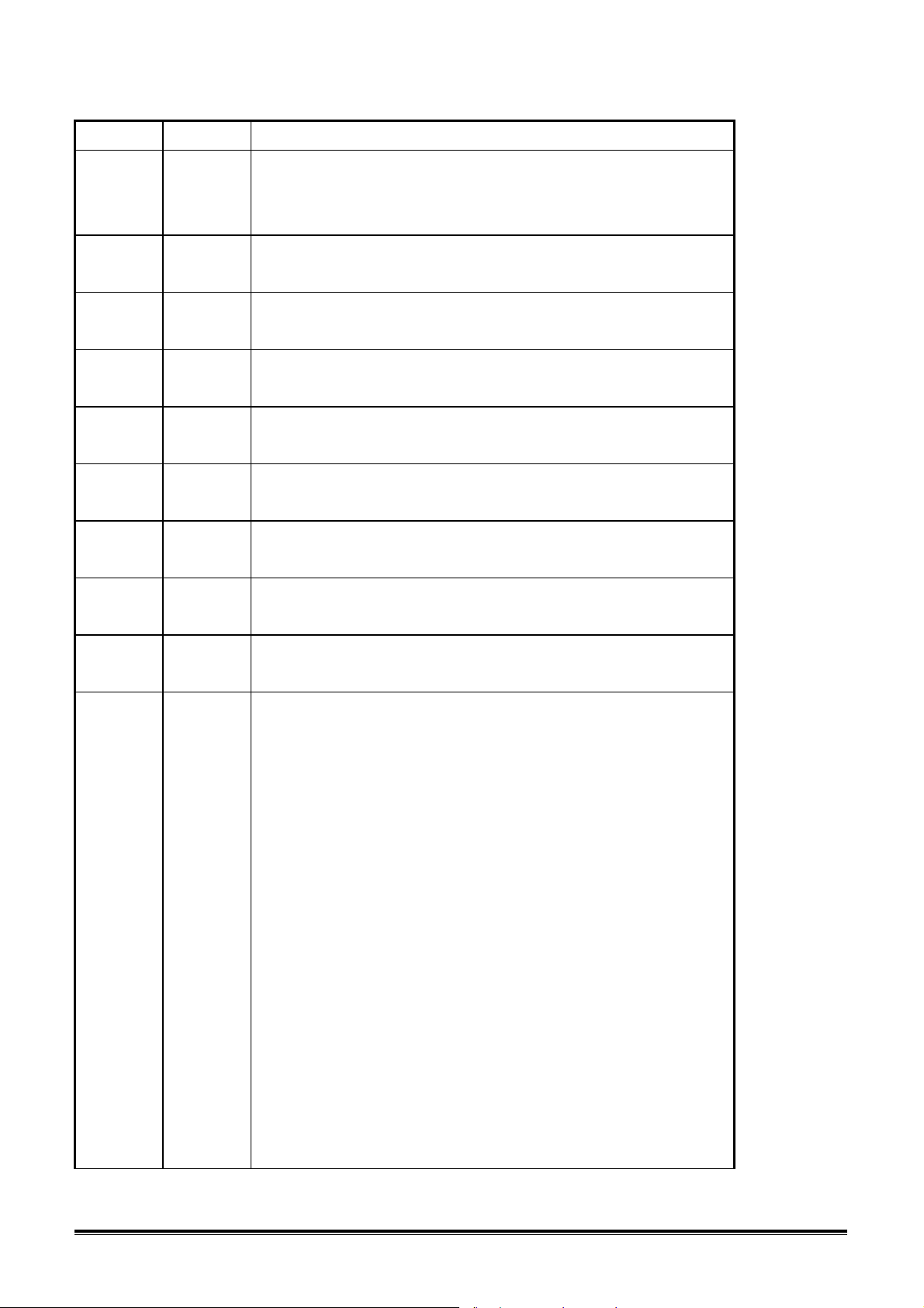
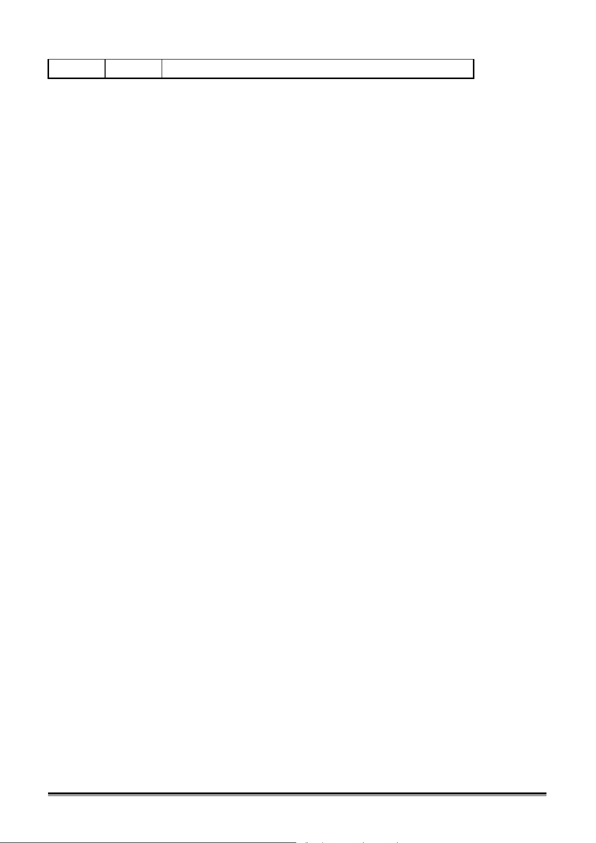
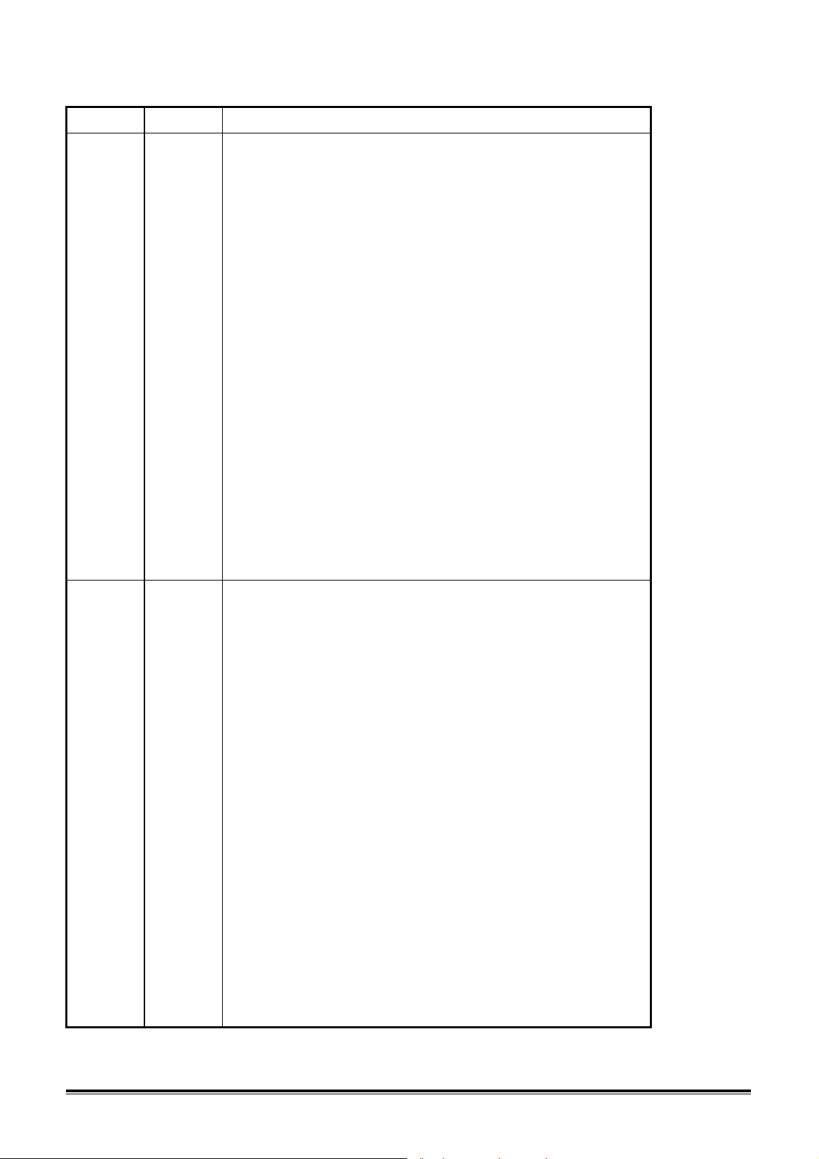
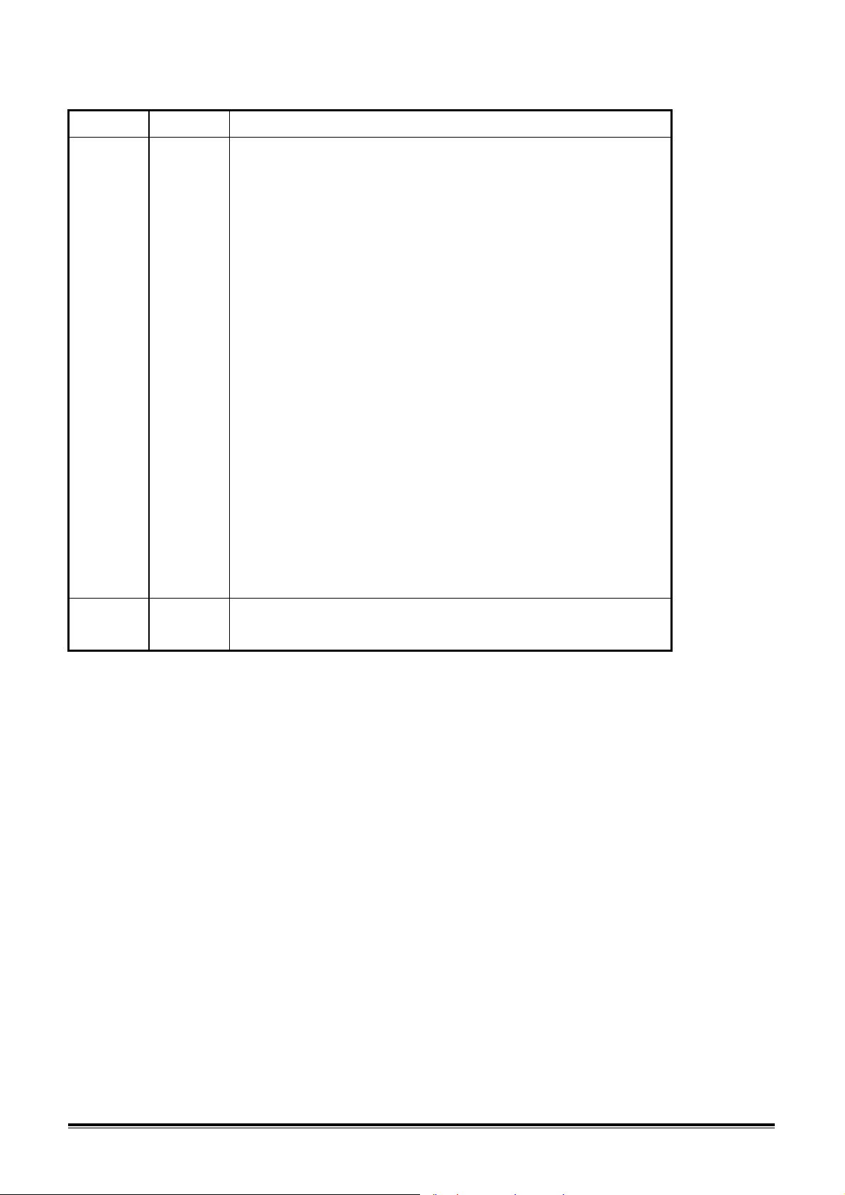
Table 1 - DDC Table
Address Data Description
00 00
01 FF
02 FF
03 FF Header
04 FF
05 FF
06 FF
07 00
08 06 ID Manufacturer Name = API
09 09
0A 05 ID Product Code = G781
0B 98 (Vender Assigned code)
0C * ID Serial Number
0D * 32 bits serial no.
0E * (use 0 if n/a)
0F *
10 * Week of Manufacture (0-53),use 0 if n/a
11 * Year of Manufacture (year - 1990)
12 01 EDID version
13 03 Revision
14 08 Video Input Define
15 1F Max. H. Image Size (cm)
16 17 Max. V. Image Size (cm)
17
18
19
1A
*
EA
*
*
(gamma*100) - 100
DPMS
Red Green Bits Rx1Rx0Ry1Ry0Gx1Gx0Gy1Gy0
Blue White Bits Bx1Bx0By1By0Wx1Wx0Wy1Wy0
1B
1C
1D
1E
1F
20
*
*
*
*
*
*
Red x bit9-2
Red y bit9-2
Green x bit9-2
Green y bits9-2
Blue x bit9-2
Blue y bit9-2
13
Page 17
MEA 1786FD2 CRT Monitor Service Guide
Engineering Specification
21
22
*
*
White x bit9-2
White y bit9-2
14
Page 18
MEA 1786FD2 CRT Monitor Service Guide
Engineering Specification
Address Data Description
23 AF Established Timing I
24 CF Established Timing II
25 00 Established Timing III
26 45 Standard Timing Identification
27 59 #1 800x600 @85Hz
28 61 #2 1024x768 @85Hz
29 59
2A 01 #3
2B 01
2C 01 #4
2D 01
2E 01 #5
2F 01
30 01 #6
31 01
32 01 #7
33 01
34 01 #8
35 01
36 EA Detailed Timing Description # 1
37 24
38 00
39 60
3A 41
3B 00
3C 28
3D 30
3E 30
3F 60
Pixel clock = 94.5Mhz
Hor. Display = 1024 pixels
Hor. Blanking = 352 pixels
Hor. Front porch = 48 pixels
Hor. Back porck = 208 pixels
Hor. Sync pulse = 96 pixels
Hor. Border = 0 pixels
Hor. Size = 310 mm
40 13
41 00
42 36
43 E6
44 10
45 00
46 00
Ver. Display = 768 lines
Ver. Blanking = 40 lines
Ver. Front porch = 1 lines
Ver. Back porch = 36 lines
Ver. Sync pulse = 3 lines
Ver. Border = 0 lines
Ver. Size = 230 mm
15
Page 19
MEA 1786FD2 CRT Monitor Service Guide
Engineering Specification
47 00
16
Page 20
MEA 1786FD2 CRT Monitor Service Guide
Engineering Specification
Address Data Description
48 00
49 00
4A 00
4B FC Monitor name=Acer G781
4C 00
4D 41 A
4E 63 c
4F 65 e
50 72 r
51 20
52 47 G
53 37 7
54 38 8
55 31 1
56 0A
57 20
58 20
59 20
5A 00 SN 00001
5B 00
5C 00
5D FF
5E 00
5F 30
60 30
61 30
62 30
63 31
64 0A
65 20
66 20
67 20
68 20
69 20
6A 20
6B 20
17
Page 21
MEA 1786FD2 CRT Monitor Service Guide
Engineering Specification
Address Data Description
6C 00
6D 00 Range limit
6E 00 V.Freq range 50-120Hz
6F FD H.Freq range 30-86KHz
70 00 Max pix clock 150 MHz
71 32
72 78
73 1E
74 56
75 0F
76 00
77 0A
78 20
79 20
7A 20
7B 20
7C 20
7D 20
7E 00 Extension Flag
7F * Check sum
18
Page 22
MEA 1786FD2 CRT Monitor Service Guide
Engineering Specification
Samsung TCO99 Tube
17
18
19
1A
1B
1C
1D
1E
1F
20
21
22
BE
*
03
94
A5
52
46
97
24
10
48
4C
(gamma*100) – 100
DPMS
Red Green Bits Rx1Rx0Ry1Ry0Gx1Gx0Gy1Gy0
Blue White Bits Bx1Bx0By1By0Wx1Wx0Wy1Wy0
Red x bit9-2
Red y bit9-2
Green x bit9-2
Green y bits9-2
Blue x bit9-2
Blue y bit9-2
White x bit9-2
White y bit9-2
Samsung MPRII Tube
17
BE
(gamma*100) – 100
18
19
1A
1B
1C
1D
1E
1F
20
21
22
*
03
9E
A5
52
46
97
24
10
47
4F
DPMS
Red Green Bits Rx1Rx0Ry1Ry0Gx1Gx0Gy1Gy0
Blue White Bits Bx1Bx0By1By0Wx1Wx0Wy1Wy0
Red x bit9-2
Red y bit9-2
Green x bit9-2
Green y bits9-2
Blue x bit9-2
Blue y bit9-2
White x bit9-2
White y bit9-2
19
Page 23
MEA 1786FD2 CRT Monitor Service Guide
Engineering Specification
Philips MPRII Tube
17
18
19
1A
1B
1C
1D
1E
1F
20
21
22
A7
*
94
AE
9E
58
4A
9C
27
10
47
4F
(gamma*100) – 100
DPMS
Red Green Bits Rx1Rx0Ry1Ry0Gx1Gx0Gy1Gy0
Blue White Bits Bx1Bx0By1By0Wx1Wx0Wy1Wy0
Red x bit9-2
Red y bit9-2
Green x bit9-2
Green y bits9-2
Blue x bit9-2
Blue y bit9-2
White x bit9-2
White y bit9-2
Philips TCO99 Tube
17
A7
(gamma*100) – 100
18
19
1A
1B
1C
1D
1E
1F
20
21
22
*
94
A4
9E
58
4A
9C
27
10
48
4C
DPMS
Red Green Bits Rx1Rx0Ry1Ry0Gx1Gx0Gy1Gy0
Blue White Bits Bx1Bx0By1By0Wx1Wx0Wy1Wy0
Red x bit9-2
Red y bit9-2
Green x bit9-2
Green y bits9-2
Blue x bit9-2
Blue y bit9-2
White x bit9-2
White y bit9-2
20
Page 24
MEA 1786FD2 CRT Monitor Service Guide
Engineering Specification
ChungHwa MPRII Tube
17
18
19
1A
1B
1C
1D
1E
1F
20
21
22
C3
*
EB
2E
A2
55
47
99
25
0F
47
4F
(gamma*100) – 100
DPMS
Red Green Bits Rx1Rx0Ry1Ry0Gx1Gx0Gy1Gy0
Blue White Bits Bx1Bx0By1By0Wx1Wx0Wy1Wy0
Red x bit9-2
Red y bit9-2
Green x bit9-2
Green y bits9-2
Blue x bit9-2
Blue y bit9-2
White x bit9-2
White y bit9-2
Note 1
Bit Bit Description
7 Analog / Digital Signal Level
6 Signal Level Standard (6)
5 Signal Level Standard (5)
4 Setup
3 Sync Inputs Supported (3)
2 Sync Inputs Supported (2)
1 Sync Inputs Supported (1)
0 Sync Inputs Supported (0)
21
Page 25
MEA 1786FD2 CRT Monitor Service Guide
Engineering Specification
Bit Description
7 Analog / Digital Input : Defines usage of the rest if the byte as "analog input" or
digital input". Analog=0, Digital=1 .
If input is described as analog, the following definitions apply to bits 6-0.
6:5 Signal Level Standard (6:5) : Refer to the following bit definitions. Identified by the
level of reference white volts above blank, followed by the level of the sync tips in
volts below
blank.
Bit 6 Bit 5 Operation
0 0 0.700V/0.300V (1.000V p-p)
0 1 0.714V/0.286V (1.000V p-p)
1 0 1.000V/0.400V (1.400V p-p)
1 1 Reserved; TBD
4 Setup: If set, the display is set to expect a blank-to-black setup or pedestal per the
appropriate signal level standard.
3:0 Sync Inputs (See Bit Operation below)
3 Separate Sync
2 Composite Sync (on H Sync line)
1 Sync on Green Video
0 Serration of the V.Sync Pulse is required when composite sync or
sync-ongreen video is used
22
Page 26
MEA 1786FD2 CRT Monitor Service Guide
Engineering Specification
Note 2
Bit 7 Stand-by
Bit 6 Suspend
Bit 5 Active off
Bit
4:3
0,0 - Monochrome/gray scale display
Bit
2:0
Display Type
0,1 - RGB color display
1,0 - Non-RGB multicolor display (example:RGY)
1,1 - Undefined.
Reserved. Set at 00h until defined.
Note 3
SAMSUNG 0.645/0.321 0.274/0.593 0.143/0.064 2.9
CRT Vender Red (x/y) Green (x/y) Blue (x/y) Gamma
23
Page 27
MEA 1786FD2 CRT Monitor Service Guide
Engineering Specification
Note 4
Byte 1 bit Established Timings 1 Source
7 640*400 @ 70Hz (720x400) (VGA, IBM)
6 720*400 @ 88Hz (XGA2, IBM)
5 640*480 @ 60Hz (VGA, IBM)
4 640*480 @ 67Hz (Mac II, Apple)
3 640*480 @ 72Hz (VESA)
2 640*480 @ 75Hz (VESA)
1 800*600 @ 56Hz (VESA)
0 800*600 @ 60Hz (VESA)
Byte 2 bit Established Timings II
7 800*600 @ 72Hz (VESA)
6 800*600 @ 75Hz (VESA)
5 832*624 @ 75Hz (Mac II, Apple)
4 1024*768 @ 87Hz (interlaced) (IBM)
3 1024*768 @ 60Hz (VESA)
2 1024*768 @ 70Hz (VESA)
1 1024*768 @ 75HZ (VESA)
0 1280*1024 @ 75HZ (VESA)
Byte 3 bit Manufacturer's Timings Manufacturer's Specified Timing
7 1152*870 @ 75Hz (Mac II, Apple)
6 640*480 @ 85HZ
5 800*600 @ 85HZ
4 1024*768 @ 85HZ
3 1280*1024 @ 85HZ
2 1600*1200 @ 75HZ
1 1600*1200 @ 85HZ
0 Flag If set = 1,then bits 6 - 1 (inclusive) should be
interpreted as Manufacture Timings as EDID
Ver 1 Rev 0.
24
Page 28
MEA 1786FD2 CRT Monitor Service Guide
Engineering Specification
Table 2 - CRT Blemish & Scratch Spec
The following criteria is applied to high-contrast blemishes.
Blemishes
A 1 trio 1 1 2 --- --B (1) 0 0 0 --- ---
(2) 0 2 2 --- 20 C
(3) 1 2 2 --- 20
D 1 dot
(1) 3 or more consecutive same color phosphor dots.
(2) 2 consecutive same color phosphor dots.
(3) 2 consecutive different color phosphor dots.
Green 3 4
Blue 5 6
Allowable No. of Blemishes Allowable
Zone
A
Red 5 6
Zone
B
Total
(Zones A & B )
6
Minimum
Separation
Zone A Zone B
50
20
Table 3 - OSD Menu
Please refer to Release 001-C01
25
Page 29
MEA 1786FD2 CRT Monitor Service Guide
X5
Engineering Specification
Table 4 - Geometry Fig.
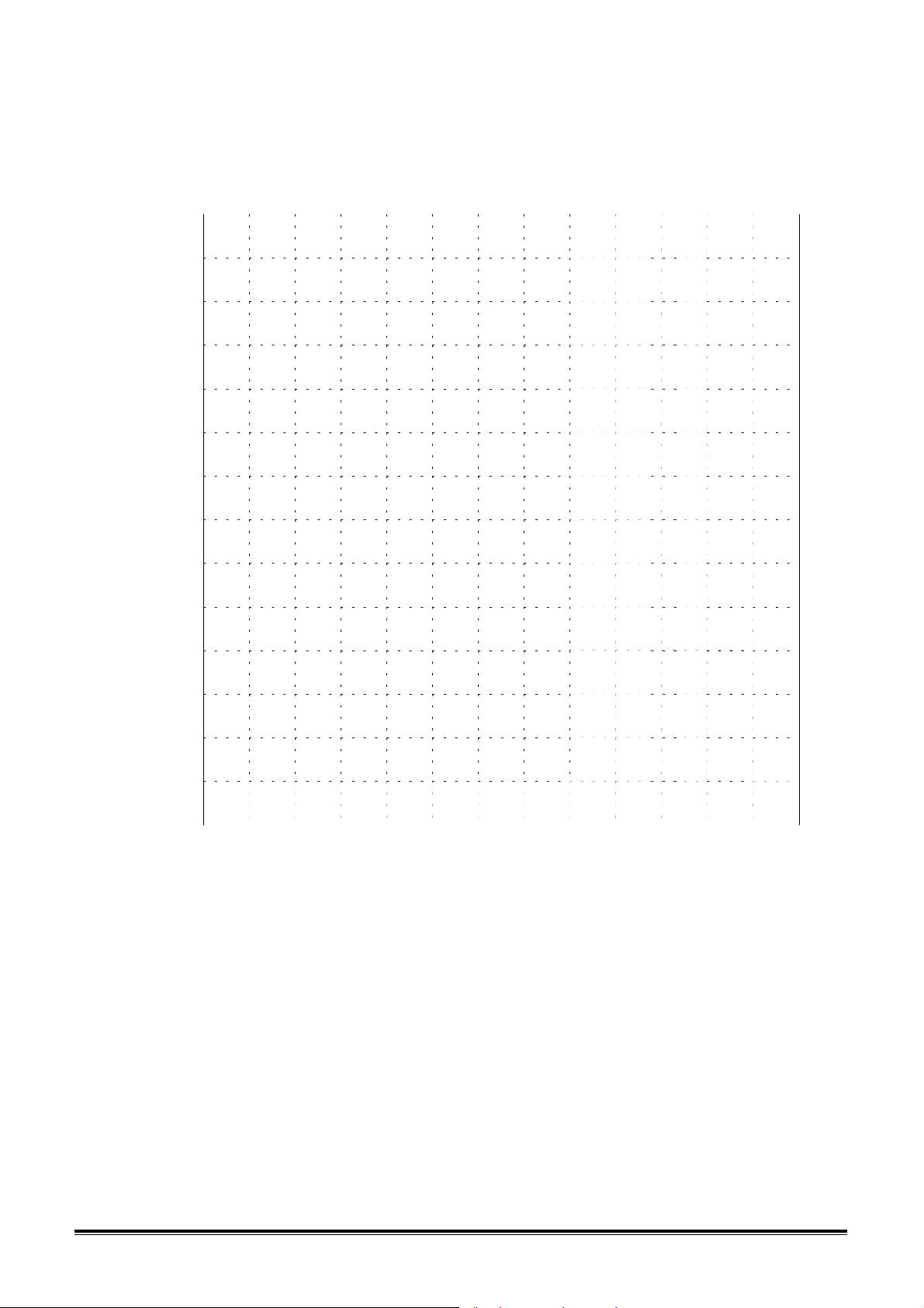
Fig.1 Linearity Measurements
X1 X2 X3 X4 X6 X7 X8 X9 X10 X11 X18
Y0
+ + + + + + + + + + + +
Y1
+ + + + + + + + + + + +
Y2
+ + + + + + + + + + + +
Y3
+ + + + + + + + + + + +
Y4
+ + + + + + + + + + + +
Y5
+ + + + + + + + + + + +
Y6
+ + + + + + + + + + + +
Y7
+ + + + + + + + + + + +
Y8
+ + + + + + + + + + + +
Y9
+ + + + + + + + + + + +
Y10
+ + + + + + + + + + + +
Y11
+ + + + + + + + + + + +
Y12
+ + + + + + + + + + + +
Y13
Xmax - Xmin
------------------- x 100% <= 5%
Xmax + Xmin
Ymax - Ymin
------------------- x 100% < =5%
Ymax + Ymin
26
Page 30
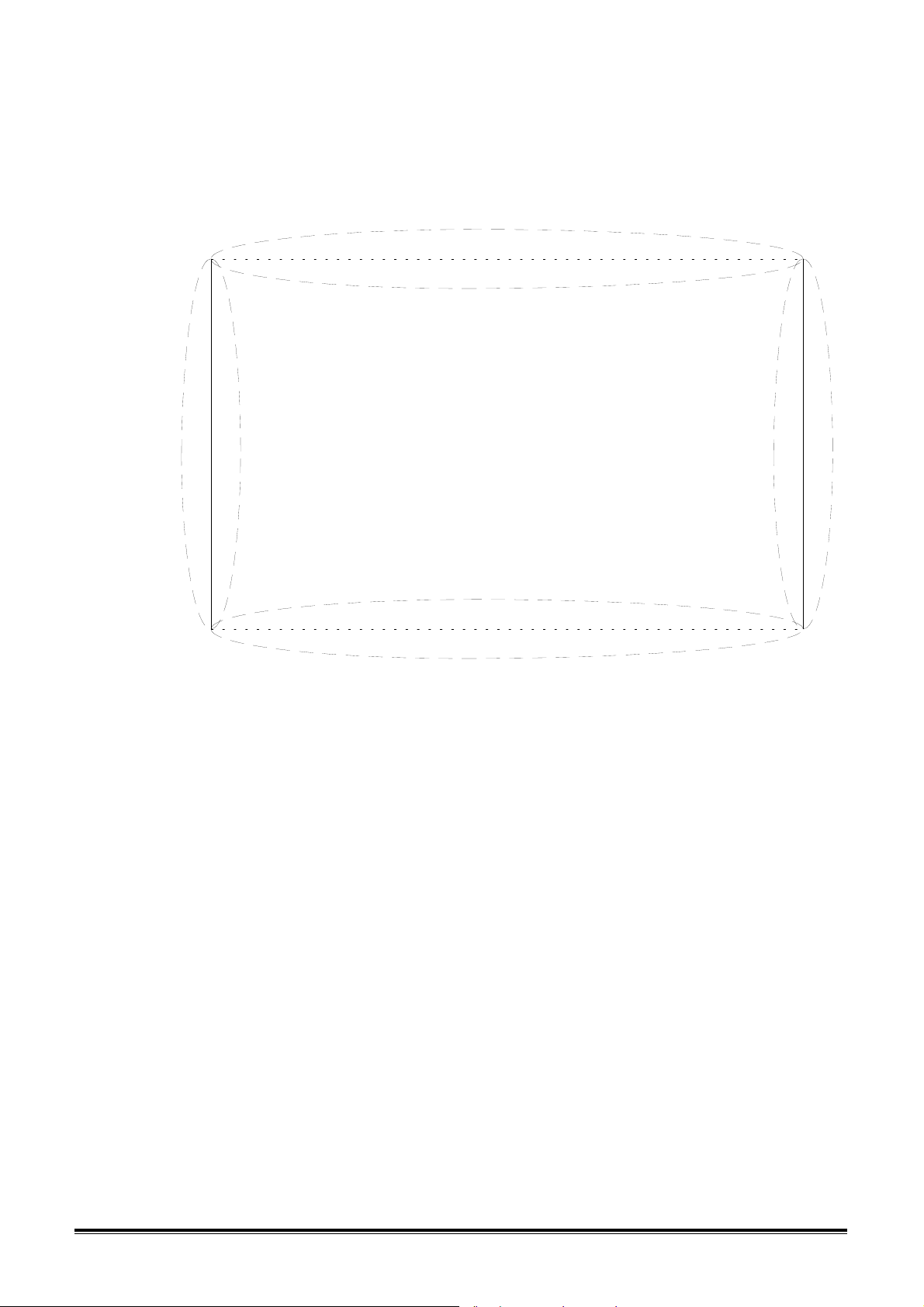
MEA 1786FD2 CRT Monitor Service Guide
Q
Engineering Specification
Fig.2 General Pincushion Measurements
Amm
a1
P
S
Bmm b1
b2
A, B represented as display area width and height
Top/Bottom Pincushion = (a1 or a2)
Side Pincushion = (b1 or b2)
Substituted A by (PS + QR)/2
B by (PQ + RS)/2
a2
R
27
Page 31
MEA 1786FD2 CRT Monitor Service Guide
Engineering Specification
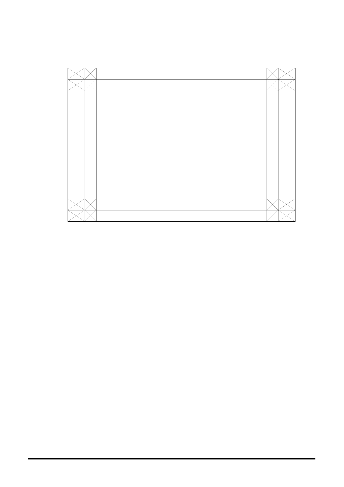
Fig.3 Trapezoid Measurements
2.5
2.5
A
B
2.5
2.5
D
C
2.5
2.5
2.5
2.5
* Each of the 4 corners of picture shall fall within the relevant area (F) illustrated up (hatched)
* ABCD is the picture outlines.
28
Page 32
MEA 1786FD2 CRT Monitor Service Guide
Engineering Specification
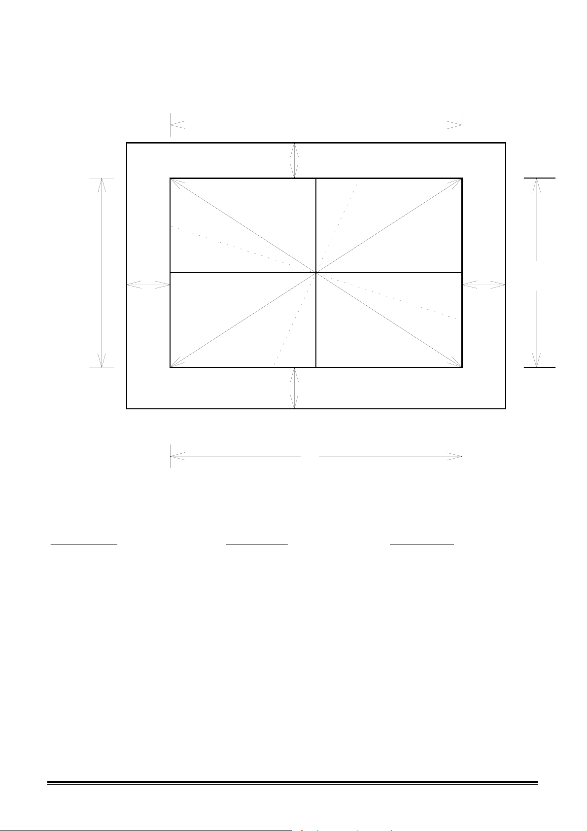
Fig.4 Picture Distortion & Phase Measurements
H1
A
a1
orthogoal
D1
V1
C D
b2
b1
D2
Tilt
V2
a2
B
PeakTotal
H2
]21|
HH
+−HH
02.0
≤
)21(5.0
]21|
VV
+−VV
02.0
≤
)21(5.0
]21|
DD
+−DD
≤
)21(5.0
03.0
29
Page 33
MEA 1786FD2 CRT Monitor Service Guide
G
Engineering Specification
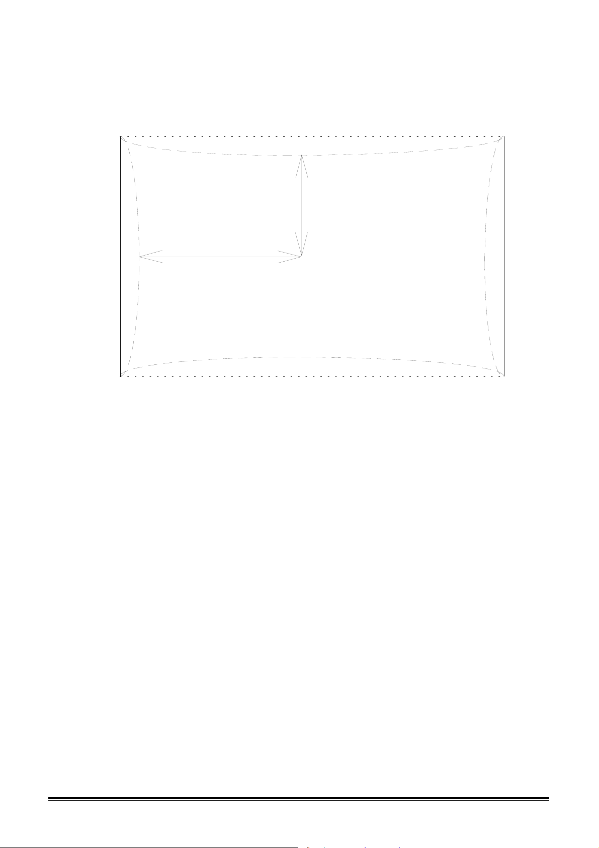
Fig.5 TCO 99 Pincushion Measurements
AC
∆
y1
B
y
x
x1
∆
∆
x2
[AC+EG]/2, [AG+CE]/2 represented as display area width and height
Top/Bottom Pincushion = ∆y1 or ∆y2
Side Pincushion = ∆x1 or ∆x2
Linearity (TCO99) = ∆x1/x or ∆y1/y
∆
y2
E
30
Page 34
MEA 1786FD2 CRT Monitor Service Guide
Engineering Specification
Fig.6 TCO 99 Barreling Measurements
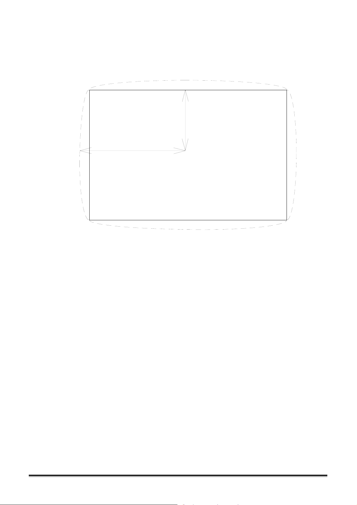
∆
AC
x1
∆
x
y1
y
∆
x2
∆
y2
EG
[AC+EG]/2, [AG+CE]/2 represented as display area width and height
Top/Bottom Pincushion = ∆y1 or ∆y2
Side Pincushion = ∆x1 or ∆x2
Linearity (TCO99) = ∆x1/x or ∆y1/y
Note 5
EDID test (W2K) 8/9/2000 8:34:46 AM
EDID test (W2K): Info retrieved from edidw2k.log by TSHELL
31
Page 35

MEA 1786FD2 CRT Monitor Service Guide
Engineering Specification
Pooltag Disabled
EDID Test Log file opened 08/09/00 - 08:34:38
EDID Dump follows:
******************* CheckSum validation *******************
PASS - Checksum valid - Proceeding with test
***********************************************************
128 bytes EDID Data (Hex):
0 1 2 3 4 5 6 7 8 9
0: 00 FF FF FF FF FF FF 00 06 09
10: 05 98 00 00 0F 00 00 0A 01 03
20: 08 1F 17 BE EA 03 9E A5 52 46
30: 97 24 10 47 4F AF CF 00 45 59
40: 61 59 01 01 01 01 01 01 01 01
50: 01 01 01 01 EA 24 00 60 41 00
60: 28 30 30 60 13 00 36 E6 10 00
70: 00 00 00 00 00 FC 00 41 63 65
80: 72 20 47 37 38 31 0A 20 20 20
90: 00 00 00 FF 00 30 30 30 30 31
100: 0A 20 20 20 20 20 20 20 00 00
110: 00 FD 00 32 78 1E 56 0F 00 0A
120: 20 20 20 20 20 20 00 AA
Monitor Type: CRT
Connector Type: VGA
Testing 17 inch monitor
Decoded EDID data
<---Header--->
veHeader: 00 FF FF FF FF FF FF 00
<-x-Header-x->
<---Vendor/Product Identification--->
32
Page 36

MEA 1786FD2 CRT Monitor Service Guide
Engineering Specification
ID Manufacturer Name:
ID Product Code:
**************** Product Code Validation ****************
PASS - Product code valid.
*********************************************************
ID Serial Number: 000F0000
Week of Manufacture: 0
Year of Manufacture: 2000
<-x-Vendor/Product Identification-x->
<---EDID Structure Version/Revision--->
EDID Version#: 1
EDID Revision#: 3
<-x-EDID Structure Version/Revision-x->
<---Basic Display Parameters/Features--->
Video i/p definition: Analog
Setup: Blank-to-Black not expected
Seperate Syncs. support: Yes
Composite Sync. support: No
Vsync. Pulse: serration not required
Max Horz Image Size: 31 cm.
Max Vert Image Size: 23 cm.
Display Gamma: 2.9
Display Type: RGB color display
Features, Preferred Timing Mode: No
Features, Preferred Timing Mode: In first detailed block
Features, GTF support: No
DPMS Features, Stand-by: Yes
DPMS Features, Suspend: Yes
DPMS Features, Active Off: Yes
33
Page 37

MEA 1786FD2 CRT Monitor Service Guide
Engineering Specification
************************ DPMS Support Check ************************
PASS - DPMS Suspend Supported
PASS - DPMS Active Off Supported
********************************************************************
<-x-Basic Display Parameters/Features-x->
<---Color Characteristics--->
Red x: 0.644531
Red y: 0.320313
Green x: 0.273438
Green y: 0.592773
Blue x: 0.142578
Blue y: 6.34766e-002
White x: 0.280273
White y: 0.310547
<-x-Color Characteristics-x->
<---Established Timings--->
Established Timimgs 1: AF
- 720x400 @70Hz
- 640x480 @60Hz
- 640x480 @72Hz
- 640x480 @75Hz
- 800x600 @56Hz
- 800x600 @60Hz
Established Timimgs 2: CF
- 800x600 @72Hz
- 800x600 @75Hz
- 1024x768 @60Hz
- 1024x768 @70Hz
- 1024x768 @75Hz
34
Page 38

MEA 1786FD2 CRT Monitor Service Guide
Engineering Specification
- 1280x1024 @75Hz
***************** Timing Support Check for 640x480 @75Hz *****************
PASS - 640x480 @75Hz support established
**************************************************************************
***************** Timing Support Check for 800x600 @75Hz *****************
PASS - 800x600 @75Hz support established
**************************************************************************
****************** Timing Support Check for 1024x768 @75Hz *****************
PASS - 1024x768 @75Hz support established
****************************************************************************
Established Timings 3: 00
<-x-Established Timings-x->
<---Standard Timing Identification--->
Standard Timing: 800x600 @85Hz
Standard Timing: 1024x768 @85Hz
<-x-Standard Timing Identification-x->
<---Detailed Timing Descriptions--->
Detailed Timing: 1024x768 @84Hz
Detailed Timing: FC (Monitor name) 'Acer G781'
Detailed Timing: FF (Monitor SN) '00001'
Detailed Timing: FD (Monitor limits)
Vert: 50 - 120 Hz
Horz: 30 - 86 KHz
Clk: 150 MHz
<-x-Detailed Timing Descriptions-x->
Extension Flag: 00
Checksum: AA
************************** EDID Test Report **************************
Congratulations - This Monitor has Passed the EDID Test
35
Page 39

MEA 1786FD2 CRT Monitor Service Guide
Engineering Specification
**********************************************************************
End of EDID Test Log
EDID Test Log file closed 08/09/00 - 08:34:46
Note 6
EDID test (W2K) 8/9/00 8:34:46 AM
EDID test (W2K): Info retrieved from edidw2k.log by TSHELL
Pooltag Disabled
EDID Test Log file opened 08/09/00 - 08:34:38
EDID Dump follows:
******************* CheckSum validation *******************
PASS - Checksum valid - Proceeding with test
***********************************************************
128 bytes EDID Data (Hex):
0 1 2 3 4 5 6 7 8 9
0: 00 FF FF FF FF FF FF 00 06 09
10: 05 98 00 00 0F 00 00 0A 01 03
20: 08 1F 17 BE EA 03 9E A5 52 46
30: 97 24 10 47 4F AF CF 00 45 59
40: 61 59 01 01 01 01 01 01 01 01
50: 01 01 01 01 EA 24 00 60 41 00
60: 28 30 30 60 13 00 36 E6 10 00
70: 00 00 00 00 00 FC 00 41 63 65
80: 72 20 47 37 38 31 0A 20 20 20
90: 00 00 00 FF 00 30 30 30 30 31
100: 0A 20 20 20 20 20 20 20 00 00
110: 00 FD 00 32 78 1E 56 0F 00 0A
36
Page 40

MEA 1786FD2 CRT Monitor Service Guide
Engineering Specification
120: 20 20 20 20 20 20 00 AA
Monitor Type: CRT
Connector Type: VGA
Testing 17 inch monitor
Decoded EDID data
<---Header--->
veHeader: 00 FF FF FF FF FF FF 00
<-x-Header-x->
<---Vendor/Product Identification--->
ID Manufacturer Name:
ID Product Code:
**************** Product Code Validation ****************
PASS - Product code valid.
*********************************************************
ID Serial Number: 000F0000
Week of Manufacture: 0
Year of Manufacture: 2000
<-x-Vendor/Product Identification-x->
<---EDID Structure Version/Revision--->
EDID Version#: 1
EDID Revision#: 3
<-x-EDID Structure Version/Revision-x->
<---Basic Display Parameters/Features--->
Video i/p definition: Analog
Setup: Blank-to-Black not expected
Seperate Syncs. support: Yes
Composite Sync. support: No
Vsync. Pulse: serration not required
Max Horz Image Size: 31 cm.
37
Page 41

MEA 1786FD2 CRT Monitor Service Guide
Engineering Specification
Max Vert Image Size: 23 cm.
Display Gamma: 2.9
Display Type: RGB color display
Features, Preferred Timing Mode: No
Features, Preferred Timing Mode: In first detailed block
Features, GTF support: No
DPMS Features, Stand-by: Yes
DPMS Features, Suspend: Yes
DPMS Features, Active Off: Yes
************************ DPMS Support Check ************************
PASS - DPMS Suspend Supported
PASS - DPMS Active Off Supported
********************************************************************
<-x-Basic Display Parameters/Features-x->
<---Color Characteristics--->
Red x: 0.644531
Red y: 0.320313
Green x: 0.273438
Green y: 0.592773
Blue x: 0.142578
Blue y: 6.34766e-002
White x: 0.280273
White y: 0.310547
<-x-Color Characteristics-x->
<---Established Timings--->
Established Timimgs 1: AF
- 720x400 @70Hz
- 640x480 @60Hz
- 640x480 @72Hz
38
Page 42

MEA 1786FD2 CRT Monitor Service Guide
Engineering Specification
- 640x480 @75Hz
- 800x600 @56Hz
- 800x600 @60Hz
Established Timimgs 2: CF
- 800x600 @72Hz
- 800x600 @75Hz
- 1024x768 @60Hz
- 1024x768 @70Hz
- 1024x768 @75Hz
- 1280x1024 @75Hz
***************** Timing Support Check for 640x480 @75Hz *****************
PASS - 640x480 @75Hz support established
**************************************************************************
***************** Timing Support Check for 800x600 @75Hz *****************
PASS - 800x600 @75Hz support established
**************************************************************************
****************** Timing Support Check for 1024x768 @75Hz *****************
PASS - 1024x768 @75Hz support established
****************************************************************************
Established Timings 3: 00
<-x-Established Timings-x->
<---Standard Timing Identification--->
Standard Timing: 800x600 @85Hz
Standard Timing: 1024x768 @85Hz
<-x-Standard Timing Identification-x->
<---Detailed Timing Descriptions--->
Detailed Timing: 1024x768 @84Hz
Detailed Timing: FC (Monitor name) 'Acer G781'
Detailed Timing: FF (Monitor SN) '00001'
39
Page 43

MEA 1786FD2 CRT Monitor Service Guide
Engineering Specification
Detailed Timing: FD (Monitor limits)
Vert: 50 - 120 Hz
Horz: 30 - 86 KHz
Clk: 150 MHz
<-x-Detailed Timing Descriptions-x->
Extension Flag: 00
Checksum: AA
************************** EDID Test Report **************************
Congratulations - This Monitor has Passed the EDID Test
**********************************************************************
End of EDID Test Log
EDID Test Log file closed 08/09/00 - 08:34:46
Table 5 - TCO 99 Spec
A. Ecology
1 General Criteria
1.1 Manufacturing Processes
1.1.1 Ozone Depleting Substances:
* PCB and any Process shall not use any ozone depleting substance.
1.1.2 Chlorinated Solvent:
* PCB and any Process shall not use any Chlorinated Solvent substance.
1.2 Environmental Hazards
1.2.1 Mercury and Cadmium in Electronic Components:
* None of electronic components contain any mercury or cadmium.
1.2.2 Flame Retardants in Plastic Components:
* Plastic > 25g shall not contain retardants of organically bound Chloride or Bromide.
1.3 Preparation for Recycling:
1.3.1 Labelling of Plastic:
* Plastic > 25g shall be labelled in accordance with ISO11469
1.3.2 Variety of Plastic:
* Plastic >100g shall be made from the same type of plastic material
1.3.3 Painting of Plastic:
* Plastic > 25g shall not be having paint weight >1% of plastic weight.
* Mould decoration (IMD) is not allowed
* All paints, lacquers, vanishes or colour additives used shall be declared by the type and mount.
40
Page 44

MEA 1786FD2 CRT Monitor Service Guide
Engineering Specification
1.3.4 Metallization of Plastic Housing:
*The plastic housing shall have neither internal nor external metallization.
41
Page 45

MEA 1786FD2 CRT Monitor Service Guide
Engineering Specification
B. CRT Display
Part 1: Visual Ergonomic - Legibility
1.3 Linearity: * <= 1%, (See Fig.5 & Fig.6)
1.4 Orthogonality:
* H/V: <= 2%, Diagonal: <= 3%
1.5.1: Display Luminance: * >=100cd/m
1.5.2 Luminance Uniformity: * < 1.5:1
1.5.3 Luminance Contrast: * > 3:1 (test at 5% of corner and center)
1.6 Front Frame Reflectance:
* Diffuse reflectance: > 20%
* Gloss <= 30% gloss unit
1.7.1: Color Temperature Variations:
* Δu'v': <+- 0.01 of White
* 9300
* 7500
* 6500
* 5000
* and actual measured Pre-set of Lower CCT should not exceed Higher CCT
o
K: 8500-10250
o
K: 6980-8100
o
K: 6100-6950
o
K: 4700-5350
o
K
o
K
o
K
o
K
2
(80% Loading)
Reference White Color Spec. in TCO’99
CCT (oK) x,y u’v’
9300 0.283, 0.297 0.189, 0.446
7500 0.299, 0.315 0.194, 0.459
6500 0.313, 0.329 0.198, 0.469
5000 0.346, 0.359 0.209, 0.488
5600
1.7.2: Color Uniformity and Characteristics:
* Δu'v': <= 0.01 (between any two point of display area (White Color))
Part 2: External Alternate Magnetic Fields:
2.1: External Alternating Magnetic Fields: * < 0.1 mm (500 mm Viewing Distance; 80Hz, 200nT.)
42
Page 46

MEA 1786FD2 CRT Monitor Service Guide
Engineering Specification
Part 3: Emission and Energy Saving
3.1 X-Ray : * < 0.5 mR/Hr
3.2 Electrostatic Potential: * <+-0.5KV
3.3 Electric Field (AC):
* Band I < 10V/m (100cd/m
* Band II< 1V/m (100cd/m
Note: Shielded Power Cord is not acceptable
3.4 Magnetic Field (AC):
* Band I < 200 nT (100cd/m
* Band II< 25 nT (100cd/m
Note: Shielded Power Cord is not acceptable
3.5 Energy Saving:
* 1st stage: <15W (recover time: 3 sec.)
2nd stage: <5W
* Single stage: <5W (recover time: <3 sec.)
* Monitor with USB Hub: same as above or single stage < 15W
(recover time < 3sec)
Part 4. Acoustic Noise:
4.1 Acoustic Noise (VDUs with fan):
* Operating: < 5.5 B (bels)
* Idle: < 4.8 B (bels)
2,
, “+” Pattern)
2,
, “+” Pattern)
2,
, “+” Pattern)
2,
, “+” Pattern)
43
Page 47
MEA 1786FD2 CRT Monitor Service Guide
y
g
p Up
p
DEFLECTION CIRCUIT OPERATION THEORY
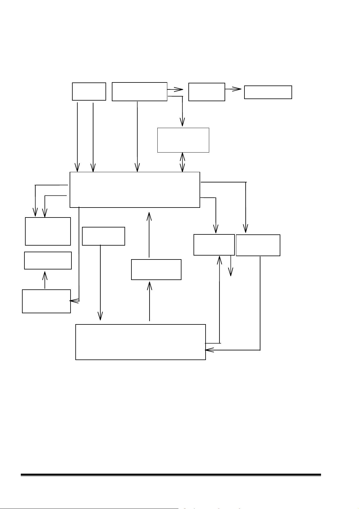
1. The Block Diagram of Deflection :
Circuit Operation Theory
H-sync
nc
V-s
Digital
Controller
Tilt
Circuit
I2C BUS
AutoSync Deflection
Controller
IC TDA4856
Ste
for B+
Dynamic
Focus
-
Shut down
Circuit
G1
Dynamic
ulation
Re
Feedback
Horizontal
Deflection Out
ut
Circuit
1
Page 48
MEA 1786FD2 CRT Monitor Service Guide
Circuit Operation Theory
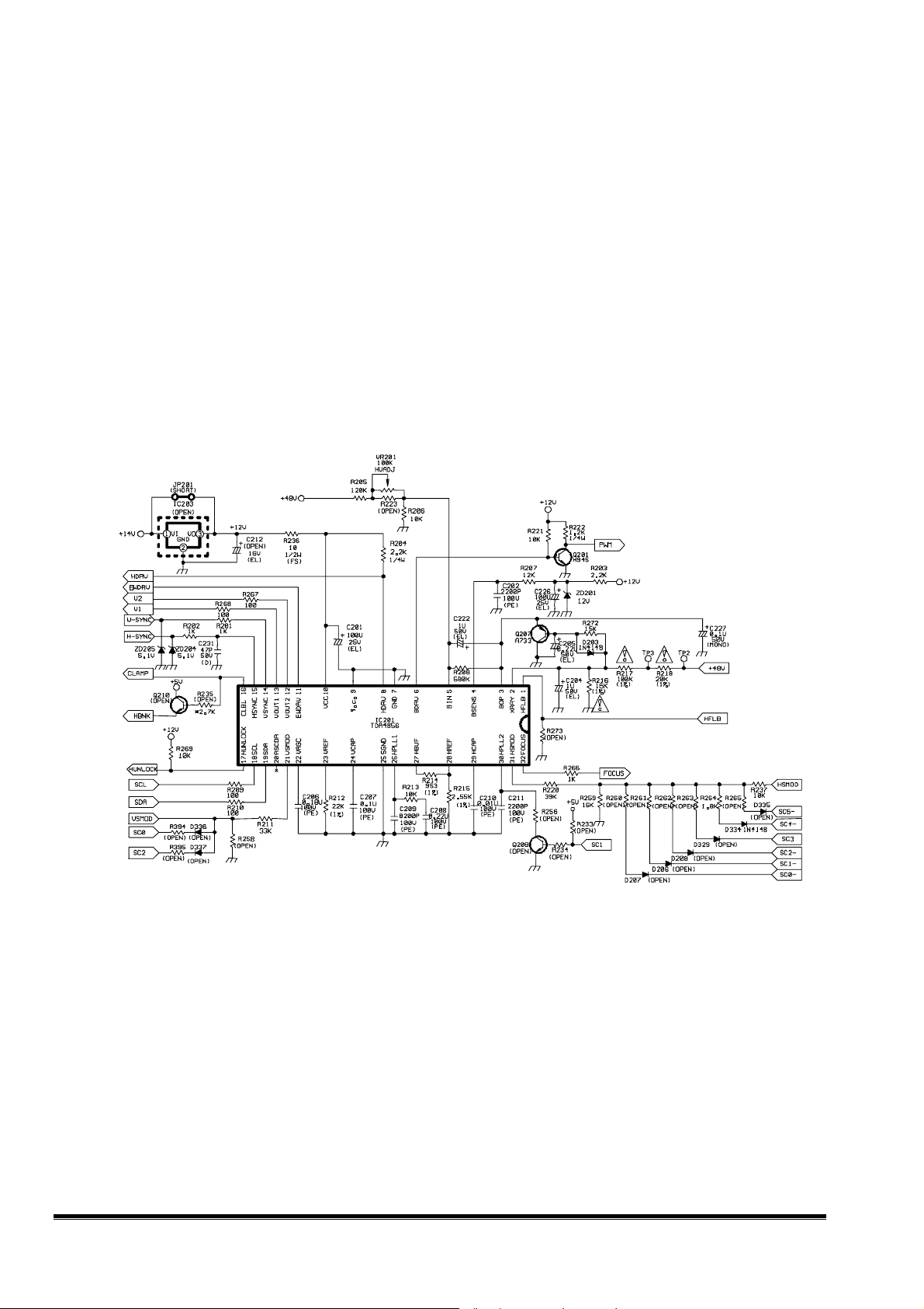
2. Autosync Deflection Controller (TDA4856)
2.1 pin 1 is AFC feedback .
2.2 pin XRAY: if V XRAY > threshold (6.25V typical) switches the whole IC into protection mode.
2.3 pin 3,4,5,6,8 for B+ control function block.
2.4 pin 11(EWDRV) is a parabolic waveform used for pincushion correction
2.5 pin 16 generates video claming & blanking pulse.
2.6 pin 18,19 is I2C data.
2.7 pin 21 V-regulation.
2.8 the resistor from pin 28 (HREF) to ground determines the maximum oscillator frequency.
2.9 the resistor from pin 27 (HBUF) to pin 28 defines the frequency range.
2.10 pin 31 H-regulation.
2.11 pin 32 focus.
Fig 2 Autosync Deflection Controller Circuit
2
Page 49
MEA 1786FD2 CRT Monitor Service Guide
Circuit Operation Theory
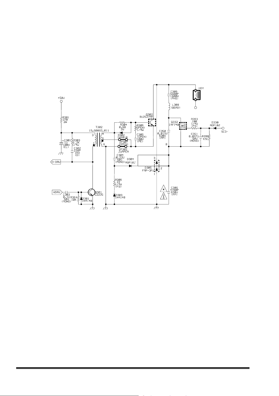
3. H-Driver & Output CKT :
3.1 HDRV signal comes from IC201 pin8 , then goes into Q301, Q301 constitutes an inverting stage
and combines with T302 to drive Q302.
3.2 Q302, C306,C309, D305, C350 constitute the H-output CKT with diode modulator mode.
Fig 3 HDRV & output circuit
3
Page 50
MEA 1786FD2 CRT Monitor Service Guide
Circuit Operation Theory
4. Dynamic focus CKT
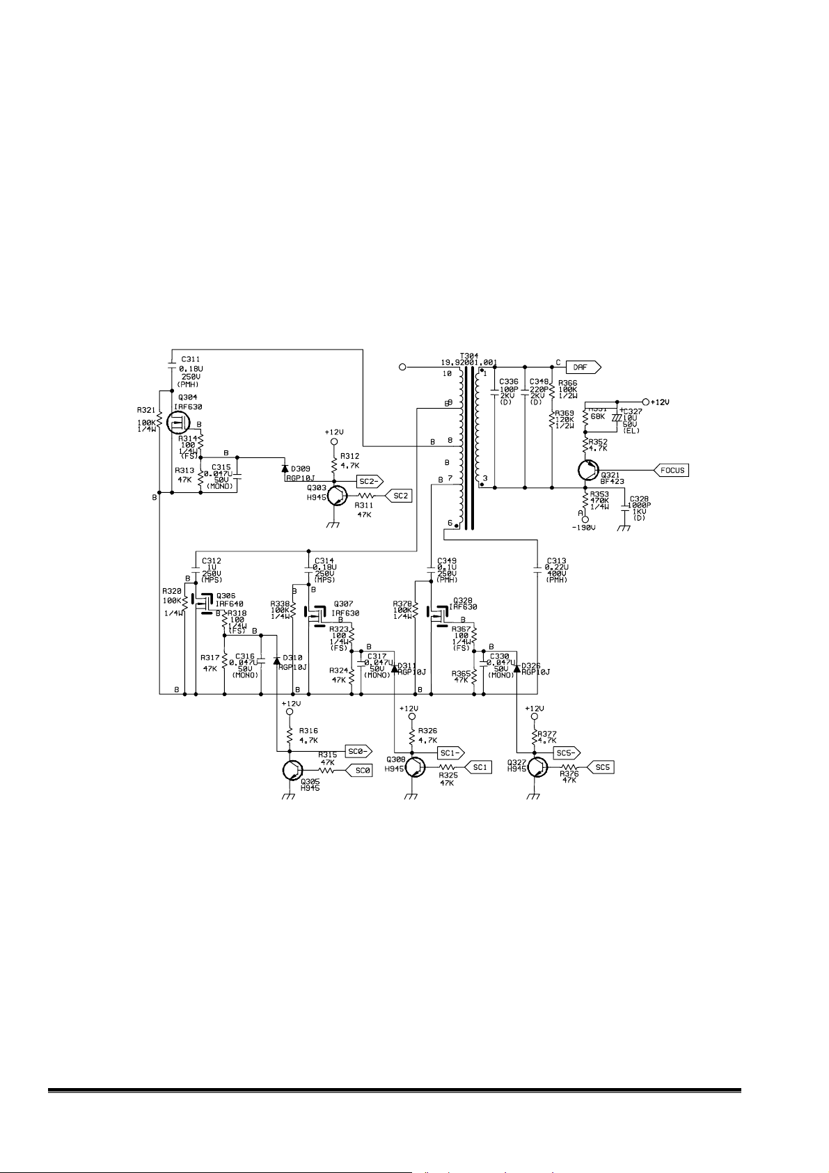
According to the CRT spec
H dynamic focus Vpp = 350 V H dynamic focus Vpp = 150 V
4-1 Vertical dynamic focus
The signal from IC201 (pin 32) is a vertical frequency parabolic waveform.
Q321 : an inverting amplifier stage.
4-2 Horizontal dynamic focus:
The horizontal frequency parabolic waveform is amplified by T304.
Fig 4 Dynamic Focus circuit
5
. Brightness & spot killer CKT.
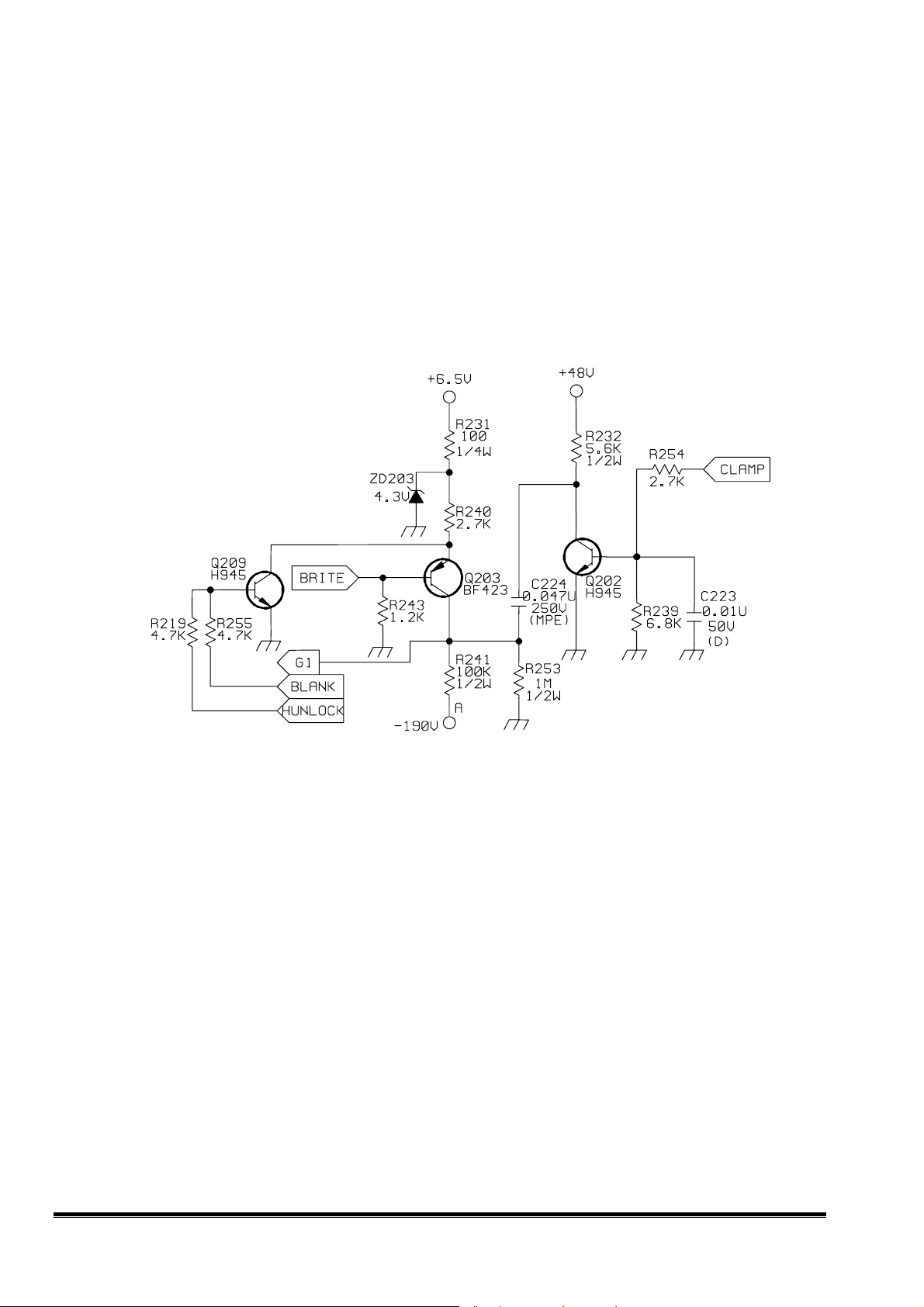
5.1 G1 CKT
The bright control signal from UC controller is about 0 ~ 5V, when the voltage of bright control signal
increases, the current flow through R241 increases and the voltage of G1 decreases.
4
Page 51
MEA 1786FD2 CRT Monitor Service Guide
Circuit Operation Theory
5.2 Blanking CKT
To avoid the disturbed picture display on the screen , we have to blank the monitor in the
following situations.
(1) when display mode is changed.
(2) when the monitor enter the power saving mode.
(3) blank the vertical retrace line
when the " blank" signal becomes "high" Q209 "ON" , Q203 "OFF".G1 voltage is about ( -190 *
R253/(R253+R241)) ≒ -184V. The signal which is IC201 (pin 16) is inverted and amplified by Q202,
and coupling to G1.During the vertical retrace interval , the G1 voltage will be drop down about 48V.
Fig5 Brite & Spotkiller circuit
5
Page 52
MEA 1786FD2 CRT Monitor Service Guide
Circuit Operation Theory
6. BDRV and step-up CKT
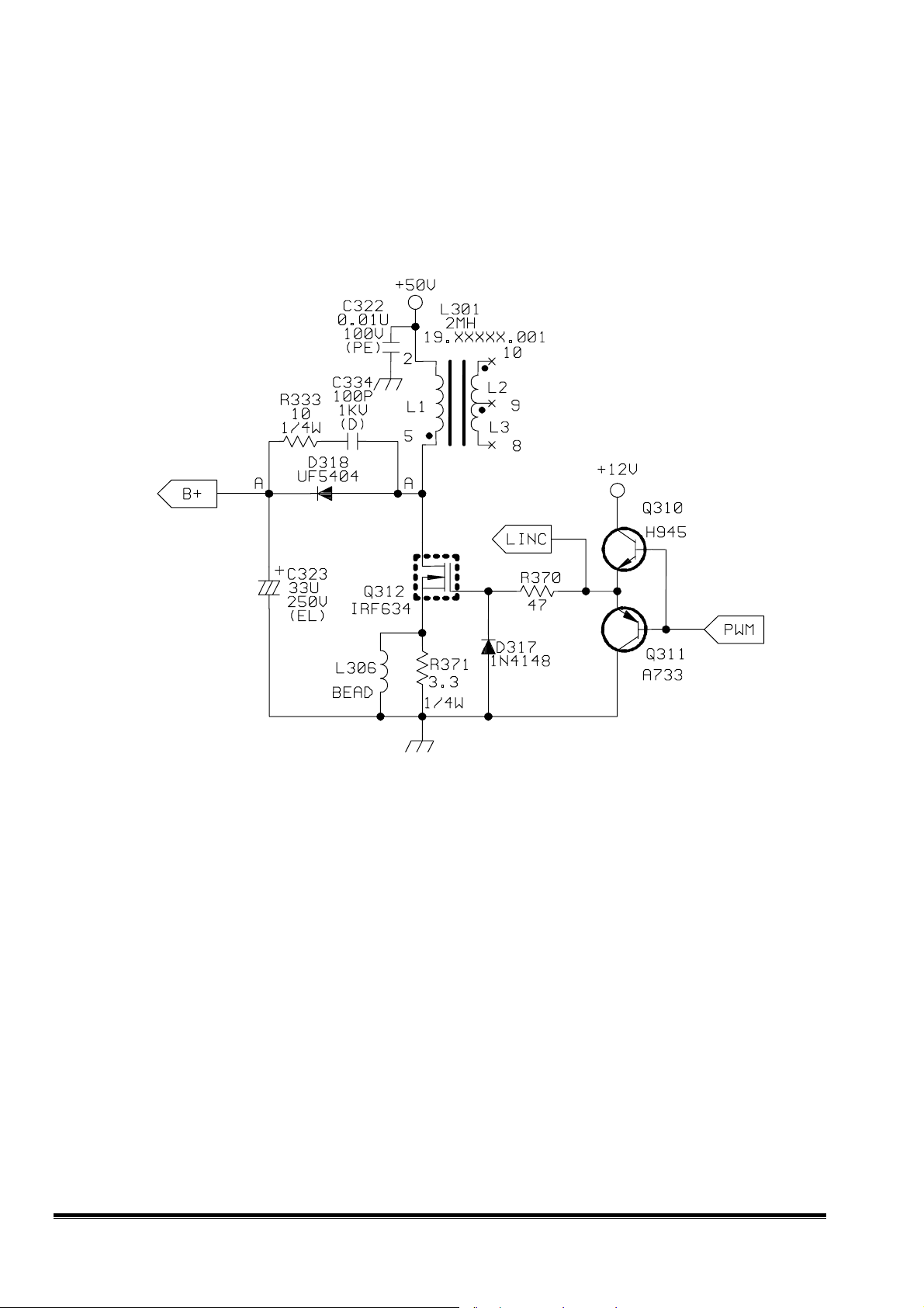
6.1 The "BDRV" signal from TDA4856 pin6 is a square waveform. It is inverted and amplified by
Q201. Q310 and Q311 constitute a buffer stage.
6.2 Q312, L301, D318, C323 is step-up circuit B+ = 50V * ( ton + toff ) / toff.
F
ig 6 BDRV & Step-up circuit
6
Page 53
MEA 1786FD2 CRT Monitor Service Guide
Circuit Operation Theory
7. HV Shutdown Circuit
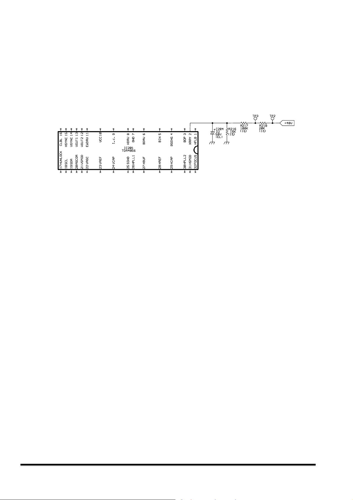
The IC201 pin2 (XRAY) provides a voltage detector with a threshold . If the voltage at pin XRAY
exceeds this threshold (6.25v typical) the pins HDRV, BDRV, VOUT1 and VOUT2 are floating.
When anode voltage increases , the voltage at FBT (pin3) increases. the voltage at IC201 pin2 increases.
The shutdown voltage is about 28KV.
Fig 7 HV- shutdown CKT
7
Page 54
MEA 1786FD2 CRT Monitor Service Guide
Circuit Operation Theory
8.Horizontal linearity CKT
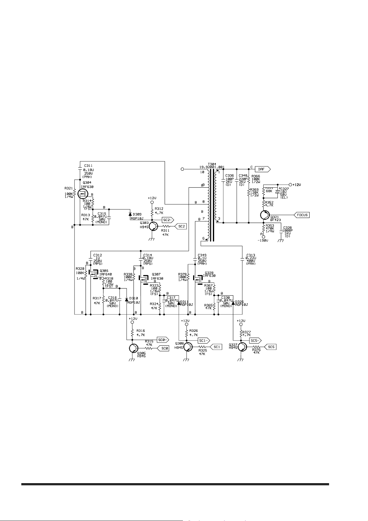
G781 Cs control truth table
Frequency range SC5 SC2 SC1 SC0 Cs Capacitor
Fh< 36K 0 0 0 0 C313 +C349+C311+C314+C312
36K<Fh<40K 1 1 1 0 C313+C312
40K<Fh<51K 0 0 0 1 C313 +C349+C311+C314
51K<Fh<62K 0 0 1 1 C313+C349+C311
62K<Fh<73K 0 1 1 1 C313+C349
73K<Fh<86K 1 1 1 1 C313
8
Fig 8 Linear circuit
Page 55
MEA 1786FD2 CRT Monitor Service Guide
Circuit Operation Theory
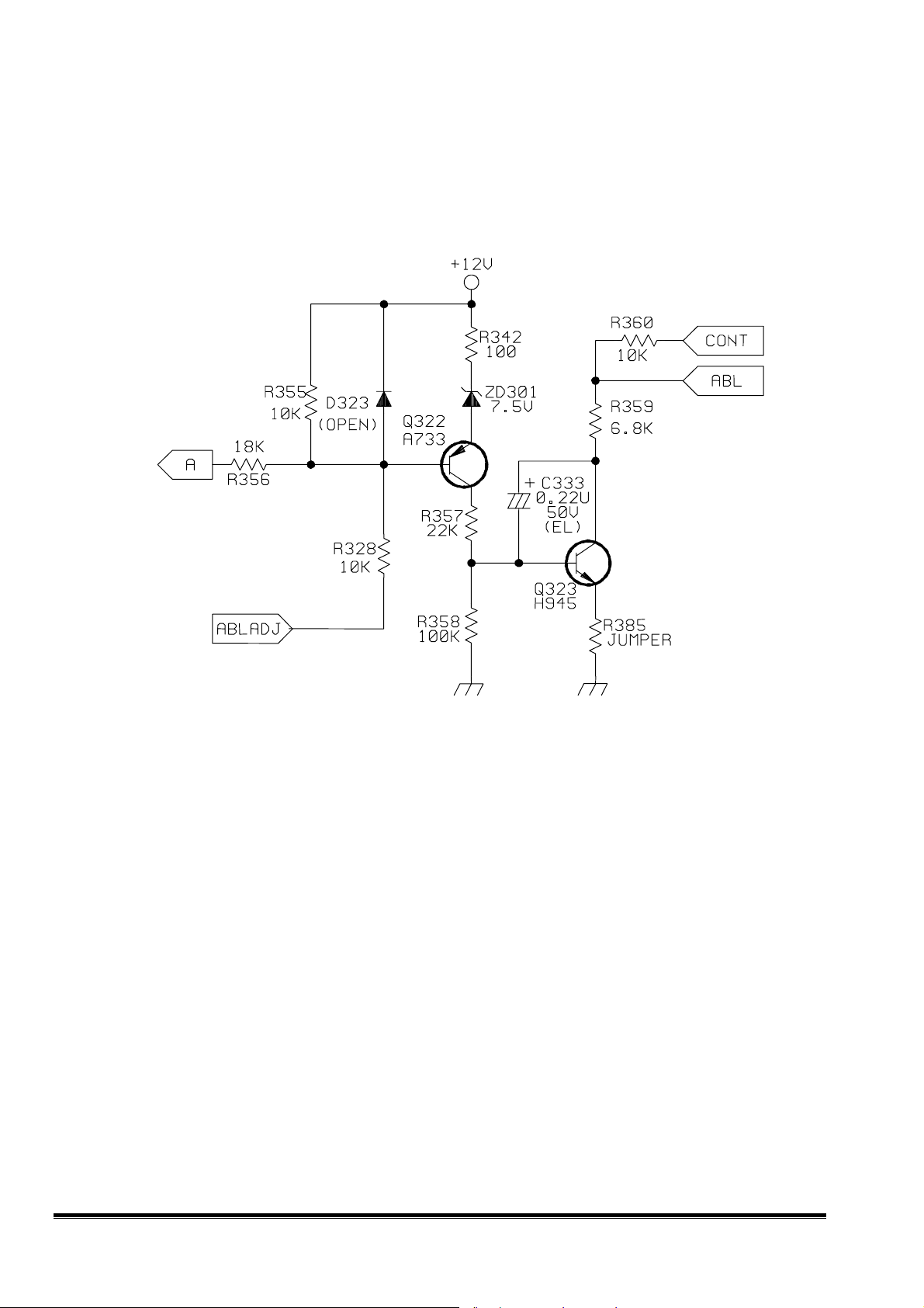
9. ABL CIRCUIT
When the beam current is over the limited current , the ABL circuit will pull down the
voltage of the video preamp (pin 11) to reduce the gain of video amplifier.
Fig 9 ABL circuit
9
Page 56
MEA 1786FD2 CRT Monitor Service Guide
Circuit Operation Theory
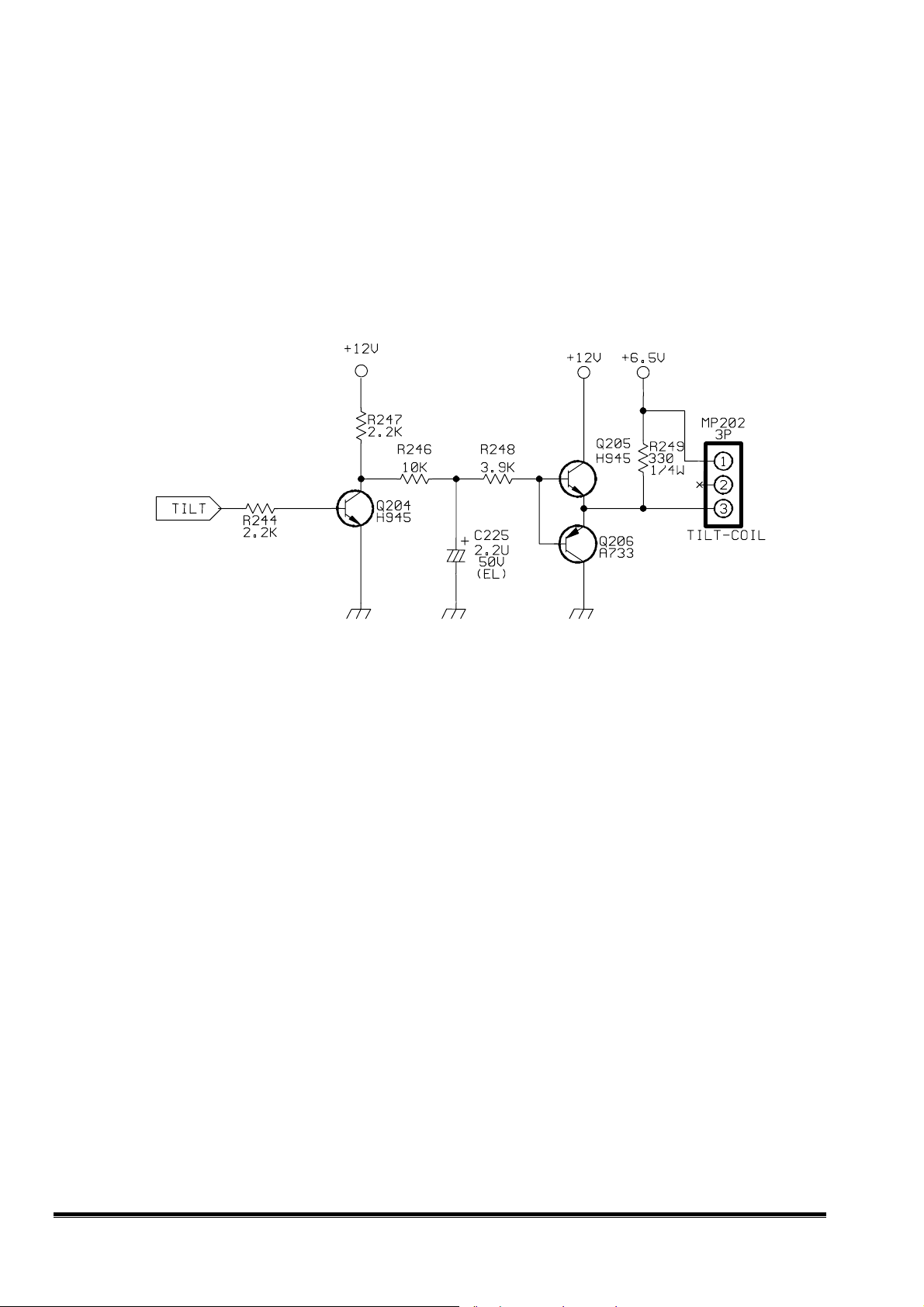
10. TILT CKT
We can rotate raster clockwise or counterclockwise by changing the direction of the current flow
through the tilt coil.
When the voltage of MP202(pin3) is larger than 6.5V, the current flows from Q205 to Tilt coil, other
wise , the current flows from tilt coil to Q206
Fig 10 TILT circuit
10
Page 57
MEA 1786FD2 CRT Monitor Service Guide
Circuit Operation Theory
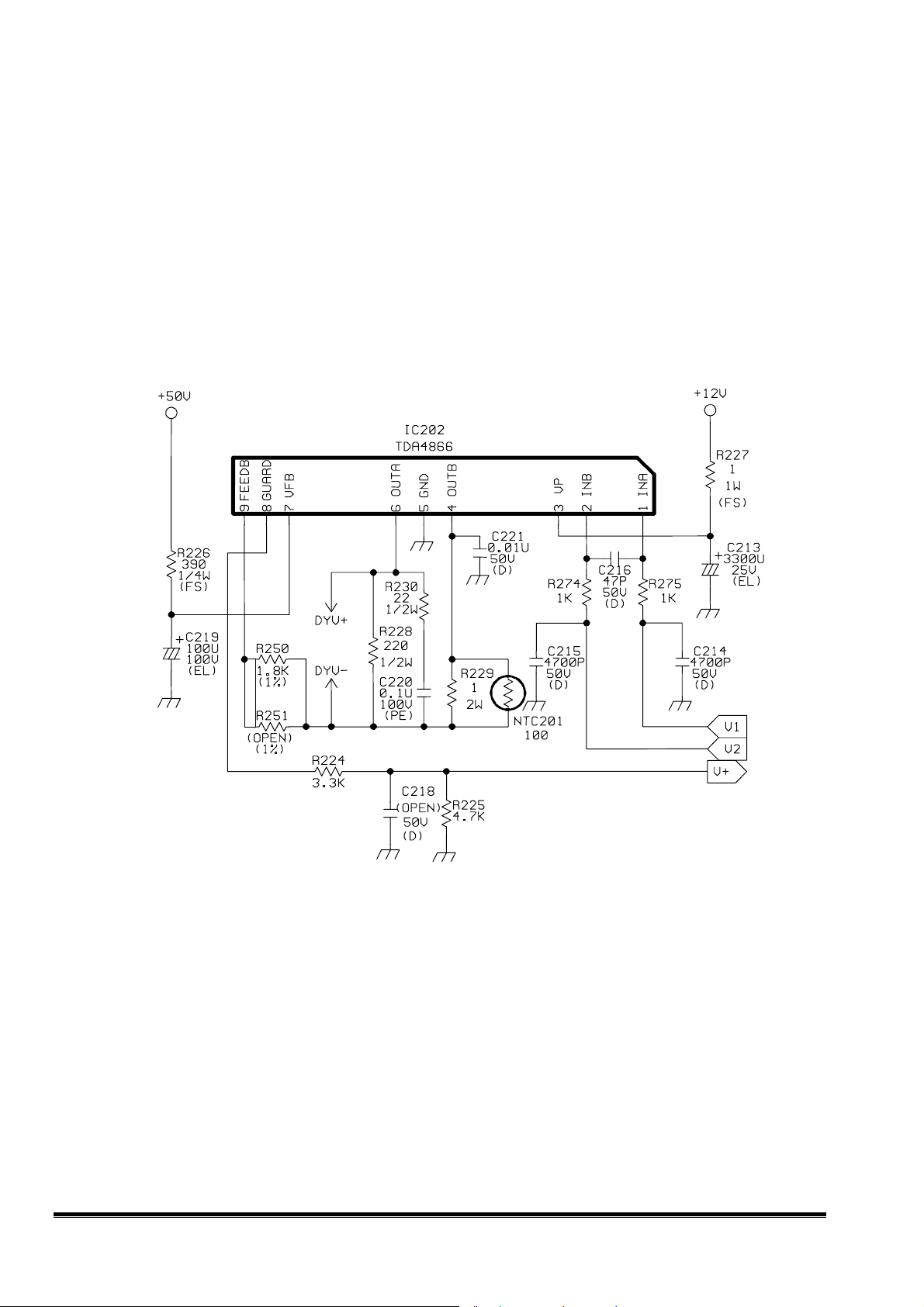
11. Vertical Output Circuit
This vertical driver IC circuit is a bridge configuration
The signals from TDA4856 differential output VOUT1 and VOUT2 are connected to TDA4866
via DC-Coupled.
The vertical deflection coil is connected between the output amplifier (TDA 4866 pin4 and
Pin6 ) ,Which are driven in phase opposite . The TDA4866 can output current to drive vertical
deflection yoke .
PIN8 ( GUARD) is used for vertical blanking.
Fig11 Vertical output circuit
11
Page 58
MEA 1786FD2 CRT Monitor Service Guide
Circuit Operation Theory
Switching Power Supply Operation Theory
1. General Specification
Input Voltage : 90~264VAC (FULL RANGE)
Input Frequency : 47~63Hz
Output Requirement: Output MAX. Load Current
+6.3V 0.7A
+13V 1.0A
+80V 0.15A
+45V 1.0A
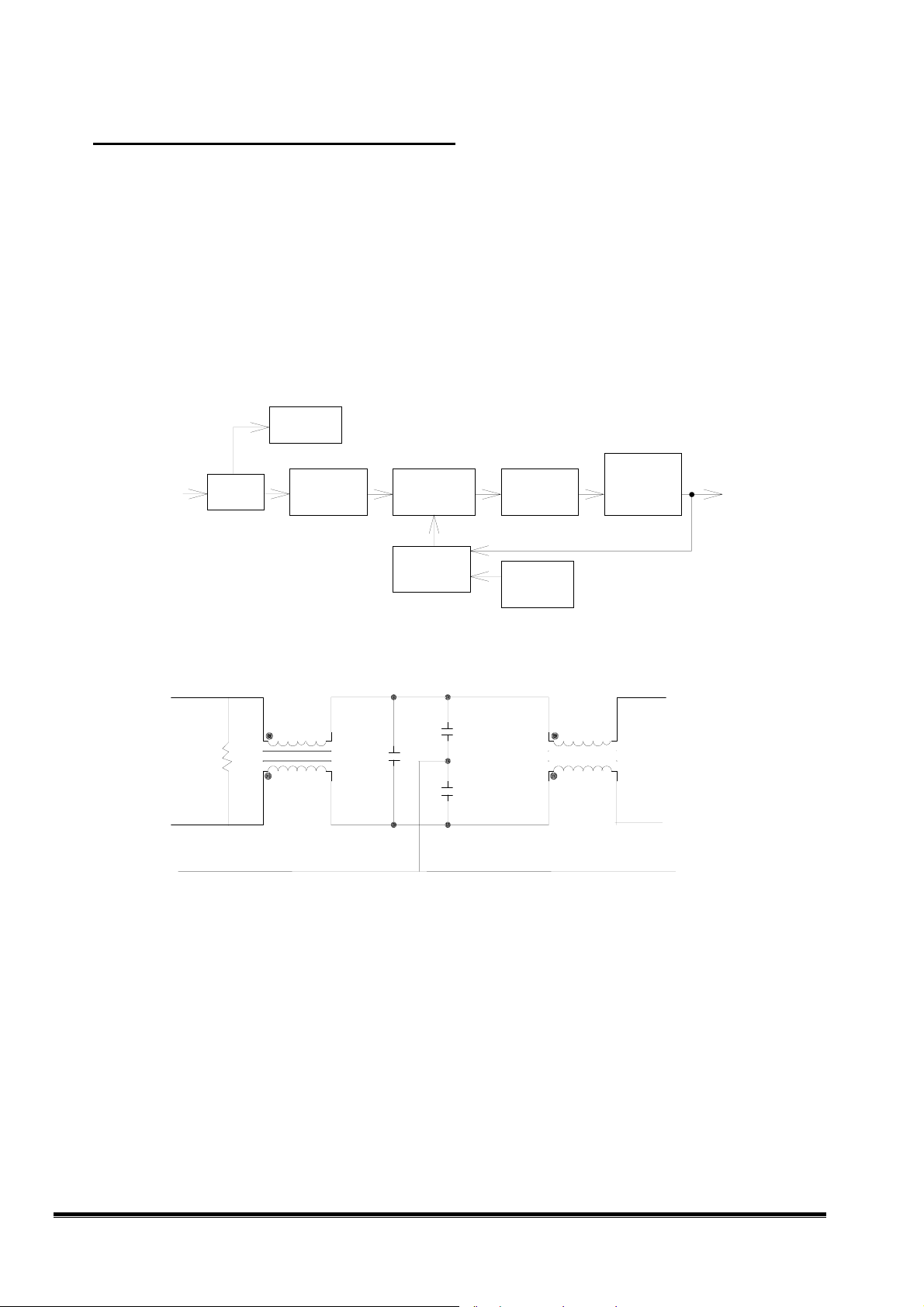
2. Block Diagram
DEGAUSS
CIRCUIT
OUTPUT
AC
INPUT
RFI
FILTER
RECTIFIER
&
FILTER
SWITCHING
ELEMENT
ISOLATION
TRANSFOR
-MER
RECTIFIER
AND
FILTER
OUTPUT
FEEDBACK
CONTROL
CIRCUIT
POWER
SAVING
CONTROL
3. Circuit Operation Theorem
3.1 RFI FILTER
FG
L
L602
34
R601
12
N
C601
0.47U
250V
(X)
C603
2200P
250V
(Y)
C602
2200P
250V
(Y)
L603
L604
This circuit designed to inhibit electric and magnetic interference for meet FCC, VDE, VCCI standard
requirements.
12
Page 59
MEA 1786FD2 CRT Monitor Service Guide
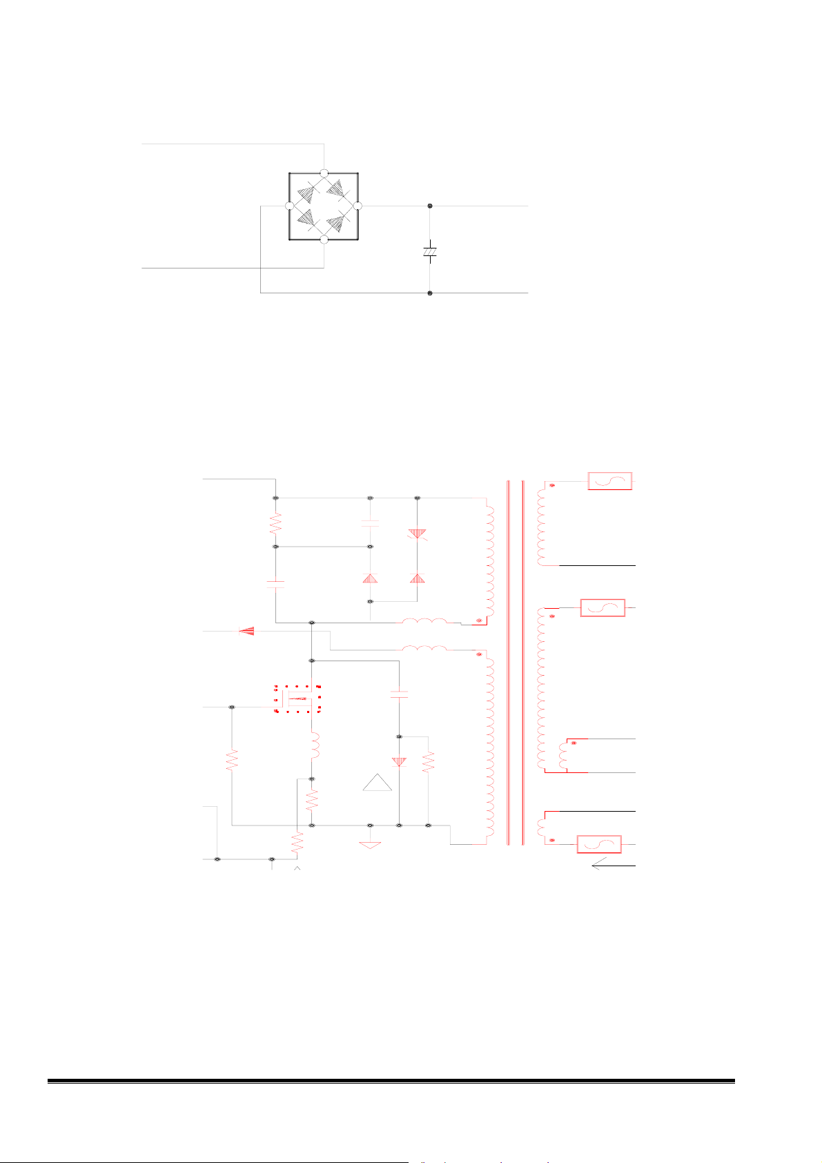
3.2 Rectifier and filter
L
3
~
AC INPUT
4
-+
D602~D605
20D6 * 4
1
Circuit Operation Theory
+
C612
220U
400V
(EL)
DC OUTPUT
~
2
N
When power switch is turn on, the AC voltage is Rectifier and filter by D602~D605, C612. The DC
output voltage will be 1.4*(ac input)
3.3 switching Element and isolation transformer
11
12
10
16
(SHORT)
13
FR701
(SHORT)
FR702
(SHORT)
15
18
FR704
C53
EGP30B
C608
47U
25V
(EL)
R604
C614
(OPEN)
D608
RGP10D
82K
2W
R608
20K
L607
(BEAD)
0.01U
C50
D610
UF4007
FS14SM-12
R611
1K
B61
C613
1KV
(D)
C51
UF4007
R607
0.15
2W
Q602
D614
*
L606
(BEAD)
L608
(BEAD)
C624
220P
T601
6
ZD601
(OPEN)
D613
(OPEN)
1
8
1KV
(D)
R619
470
2W
9
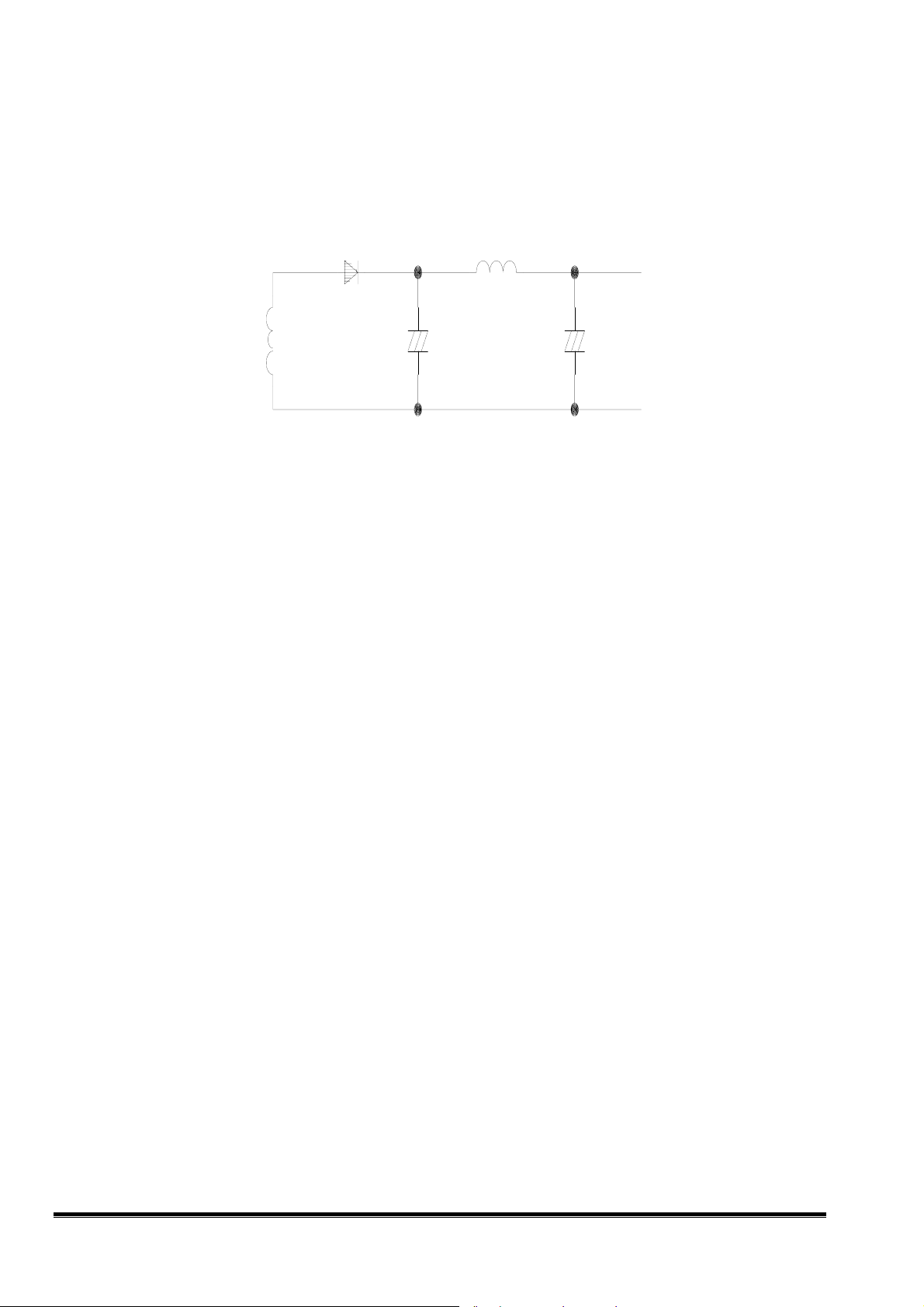
In a flyback converter operated in the discontinuous mode, the energy stored in the flyback
transformer (actually an inductor) must be zero at the beginning and end of each switching
period .
During the "ON" time, energy taken from the input is stored in the transformer when
the switching transistor turn-off, this stored energy is all delivered to the output.
13
Page 60
MEA 1786FD2 CRT Monitor Service Guide
3.4 Output Rectifier and filter
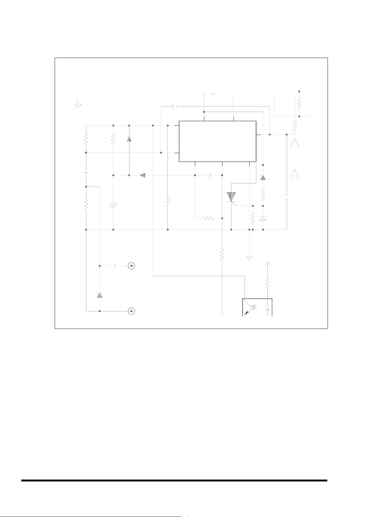
The structure of each output is illustrated as below
Circuit Operation Theory
T601
since the transformer T601 acts as a storing energy inductance, diode D1 and capacitor C1 are to
produce a dc output and additional L1, C2 to suppress high-frequency switching spikes.
D1 L1
+
C1
+
C2
14
Page 61
MEA 1786FD2 CRT Monitor Service Guide
3.5 Control circuit
Circuit Operation Theory
R613
36K
C615
2200P
50V
(PE)
R612
47
1N4004
R614
100K
C616
0.01U
100V
+
C617
4.7U
50V
(EL)
M603
D611
1N4148
D612
1N4148
C625
(OPEN)
8
4
C618
0.01U
50V
(D)
76
VCC OUT
VREF
IC601
UC3842
R/C
C619
0.022U
50V
(D)
R615
51K
R616
10K
IC603
MCR100-3 24V
A
R620
10K
ISSEN
GNDFBCOMP
GK
521
R622
510
3
ZD602
C627
+
10U
50V
(EL)
+6.5VA
R607
0.15
2W
R611
1K
*
*
C620
820P
50V
(D)
(PE)
ZD603
5.1V
4 1
M604
R738
82
1/2W
The current mode control IC UC3842 is used in the switching power supply which function of each
pin
described as follows.
pin 1 : Error amplifier output pin 5 : Ground
pin 2 : Error amplifier reverse input pin 6 : Output
pin 3 : Current sense pin 7 : VCC
pin 4 : OSC sawtooth pin 8 : Reference Voltage:5V
15
Page 62
MEA 1786FD2 CRT Monitor Service Guide
Circuit Operation Theory
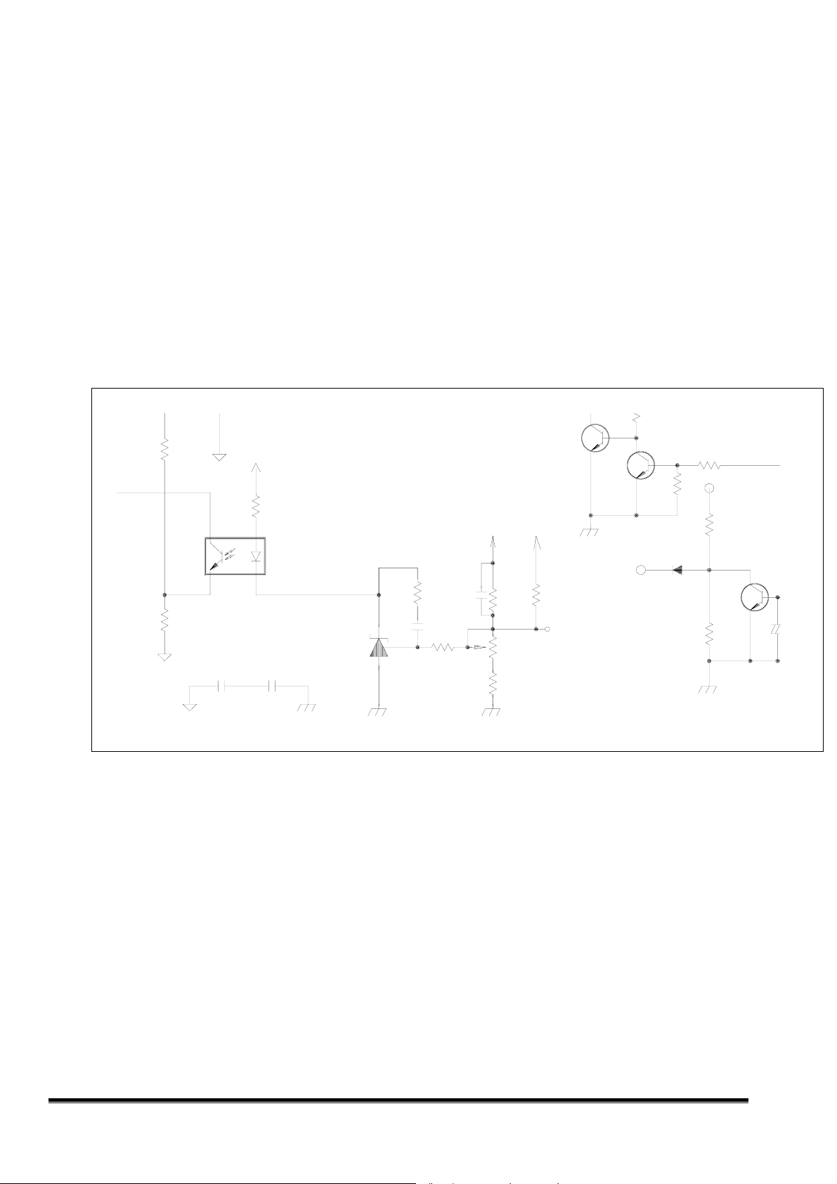
When power is initially applied to the circuit, capacitor C626 charges through R624, R623, ZD601.
When the voltage across C607 reaches a level of 16V, IC601 is turn-on the +5Vdc will be
set up at pin8 then R613, C615 generate a fixed frequency sawtooth wave to pin4, at this time
MOSFET will be drived by pin6 with square wave the pulse width of square wave is decided by
pin2 , pin3 is current feedback control, It will to sense MOSFET current. The D613, D612, R614,
C617 are soft start components to avoid the duty too large when power starts up.
3.6 Feedback circuit
This power supply adopt feedback circuit of +45V and +13V. It used IC702 for voltage regulation
and IC602 for primary-secondary isolation, The output voltage differential signal will be detected
and sensed to the pin2 of UC3842 for comparison then the duty cycle of MOSFET will be decided
to control the output voltage.
(OPEN)
R616
10K
R617
1K
4
3
IC602
TLP721F
3300P
250V
+6.5VA
R738
82
1/2W
1
2
C611C610
3300P
250V
IC702
TL431
R736
(SHORT)
C725
0.47U
50V
K
(D)
A
C730
(OPEN)
R726
R
470
+45V
R734
39K
1/4W
VR701
500
R735
1.2K
Q765
(OPEN)
SGND
+14VA
R737
20K
1/4W
REF
Q766
(OPEN)
REF
R767
(OPEN)
D766
(OPEN)
R766
(OPEN)
R768
(OPEN)
R775
(OPEN)
+6.5VA
Q767
(OPEN)
+
C766
(OPEN)
16
Page 63
MEA 1786FD2 CRT Monitor Service Guide
S
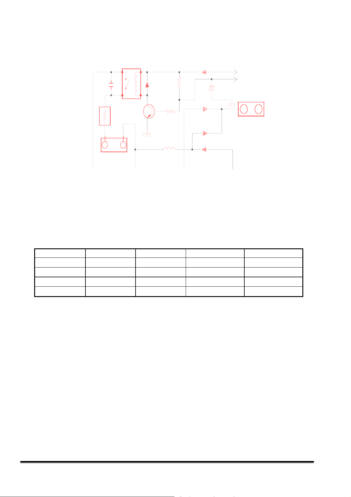
3.7 DEGAUSS CIRCUIT
Circuit Operation Theory
D709
1N4148
D603
20D6
D604
B59
20D6
D605
20D6
C708
+
47U
16V
(EL)
B60
+12V
DEGAUS
CN602
2P
12
B55
C621
2200P
250V
(Y)
213
4
RL601
TR602
2R9M
21
M602
2P
Q706
H945
1N4148
B56
TR601
8D-13
D708
R705
(OPEN)
R706
4.7K
L604
180UH
This circuit has the function of auto degaussing and manual degaussing. When power supply is
switched ON it is auto degaussing stage. When user make the selection of the manual degaussing
function in OSD, the degaussing current will flow through coil to degauss the screen of monitor.
TR602 is a PTCR to control degaussing coil current
3.8 power saving control
Mode H-sync V-sync LED Power Rating
Normal Normal Normal Green
Stand-by None Normal Orange
Suspend Normal None Orange
Off None None Orange
100﹪
≦
5W
≦
5W
≦
5W
When the H-sync or V-sync are none, the power supply +6.3v and+13v output will be cut-off.
The power input will be under 5W.
17
Page 64
MEA 1786FD2 CRT Monitor Service Guide
(
)
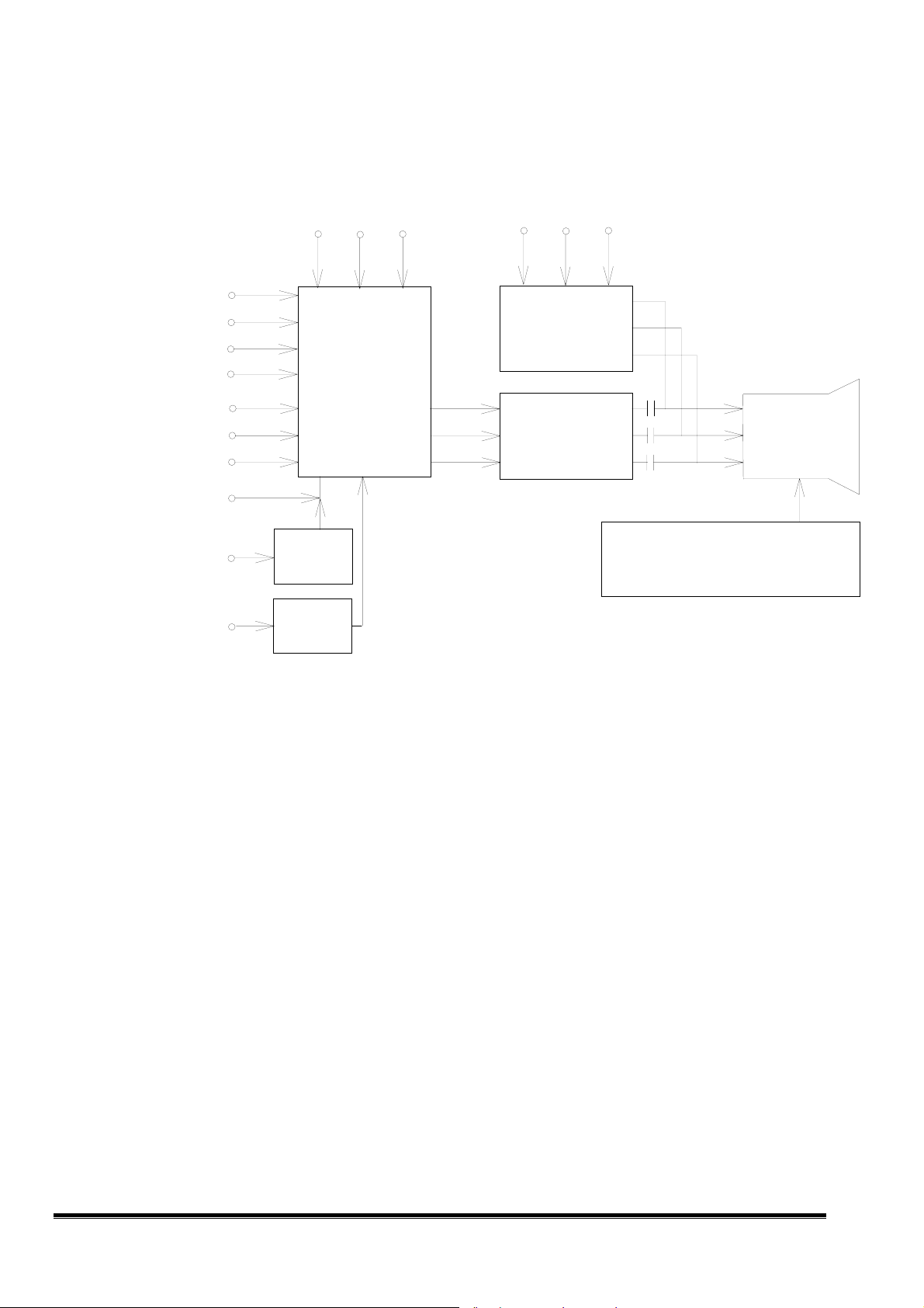
30. Video CKT
VIDEO C.K.T. BLOCK DIAGRAM
DRIVE
(FROM IC1901)
B
G
R
:
BIAS
FROM IC 1901
G
R
Circuit Operation Theory
B
R OSD
(FROM
IC 1901 )
CONTRAST
(FROM IC801)
BEAN CURRENT
(FROM F.B.T.)
H-PULSE
(FROM F.B.T.)
G OSD
B OSD
VIDEO
CUT
PREAMP
CKT
LM1279
R
G
B
IC101
ABL CKT
Q322,323
H-BLANK
CKT
Q320
DC RESTORE
Q121,122
Q141,142
Q161,162
CRT DRIVER
CKT
LM2439
IC102
BRIGHTNESS CKT: Q203
CHANGE MODE BLANK CKT:Q202
V BLANK CKT: Q202
SPOT KILLER CKT: Q202
31. OSD Preamp CKT:
(a) AS shown in the block diagram:
The R/G/B signals will generate an enough amplitude of Vpp to show up on the
CRT screen after the amplification of two amplifiers. The first one, preamp CKT,
process the signal and mix up the OSD, and the second one does the power
amplification.
(b) OSD preamp IC101, LM1279, will output the R.G.B signals seperately. The R.G.B
driver will control the gain of these three guns individually to approach the white
balance of CRT.
R
G
B
G1
(c) The signal H-Blank is to let the output of LM1279 down to 0.2V while non-display
duration. Then the CRT driver CKT will generate a level higher than Black Level. (i.e.
SYNC TIP), therefore the video signal will be blanked in order to prevent the fold over
to occure while adjusting H-phase. Besides, the SYNC TIP is used for
the DC Restoration of cascode CKT.
(d) LM1279 is equipped with OSD mixer. when signal CUT is Low, the output of
LM1279 is video signal when signal CUT goes high, the output will be OSD signal.
32. CRT DRIVER CKT:
18
Page 65

MEA 1786FD2 CRT Monitor Service Guide
Circuit Operation Theory
Output stage adopts CRT driver LM2439 to amplify the signal which has been
recessed by LM1279 to a enough amplitude of Vpp, then display on the CRT. The IC
contains three high input impedance, wide band amplifiers which directly drive the
RGB cathodes of a CRT. The gain of each channel is internally set at -15 and can
drive CRT capacitive loads as well as resistive loads presented by other application
limited only by the package’s power dissipation.
33. DC Restore CKT:
(a) The video signal amplified by the output stage is coupled to CRT by way of AC
coupling. SO DC restoration CKT is needed to do the white balance adjustment.
(b) This DC restoration circuit adopts SYNC TIP CLAMP, In the duration of
SYNC TIP the capacitor charges, and the capacitor discharge in the other time. The
Black Level is kept to the level of DC restoration setted by UC.
34. ABL CKT: (Auto Brightness Limit)
ABL is a protection circuit. When the anode current goes higher than the setting
value of ABL circuit . ABL will pull down the voltage of contrast to limit the anode
current. This is helpful to protect CRT.
35. H-BLANK CKT:
Affair the collect pulse comes from FBT being shaped and inverted, it will be sent
to preamp CKT and used as the H-Blank.
36. Brightness, V-blank, change mode blank, spotkiller CKT:
(a) About the cut off voltage , while the voltage, cathode to G1 , over the cut off ,
voltage, the picture will disappear, If cut off voltage off the CRT G Gru is
setted at 110V and the black level of cathode is 60v, the picture wont show,
the signals higher the black level once the G1 voltage is lower than-50v.
(b) As described above, we may using the voltage control G1 as the brightness
control. Generally the G1 control range is about 10~15V if the raster
brightness is form 0 to 1.5 ft-L.
(c) Similarly, we may overlap a negative pulse of vertical duration on the G1
voltage to prevent the vertical retrace line from showing on the picture , This
is to keep the voltage cathode to G1 over the cut off voltage during the
period of vertical retrace.
(d) In order to avoid the picture occur transiently while change mode, pull
down the G1 voltage and let the voltage cathode to G1 over CUT OFF voltage.
This will make the picture blanking.
(e) While monitor turned off , the discharge speed of high voltage circuit is slow
since there is no deflection scan act on the electronic beam, a spot which will
destroy the phosphor of CRT. So the SPOT KILLER circuit will generate a
19
Page 66

MEA 1786FD2 CRT Monitor Service Guide
Circuit Operation Theory
negative voltage higher than CUT OFF to the G1 to beam this is to protect
the CRT.
20
Page 67
MEA 1786FD2 CRT Monitor Service Guide
(
)
y
p
y
g
g
g
g
p
y
p
y
y
y
g
g
p
(
j
g
prog
p
SCL
SDA
HBNK
VBNK
RGB
Signal
Circuit Operation Theory
MICROCONTROLLER CIRCUIT OPERATION THEORY
1.
Introduction :
This model will support powerful OSD function to help end user fine adjustment. The
Microcontroller circuit can determine what mode it is by detecting the frequency of horizontal
and vertical synchronous and the polarity of horizontal synchronous, and provide DC voltages to
control the picture and save the adjusted value into the EEPROM by using the OSD, "On
Screen Display control", that means the user can get any information of the picture display or
adjust it and save the status values into the EEPROM by choosing and pressing the proper key
according to the indication of the OSD. In addition, user can press i-key to do auto-calibration.
2.
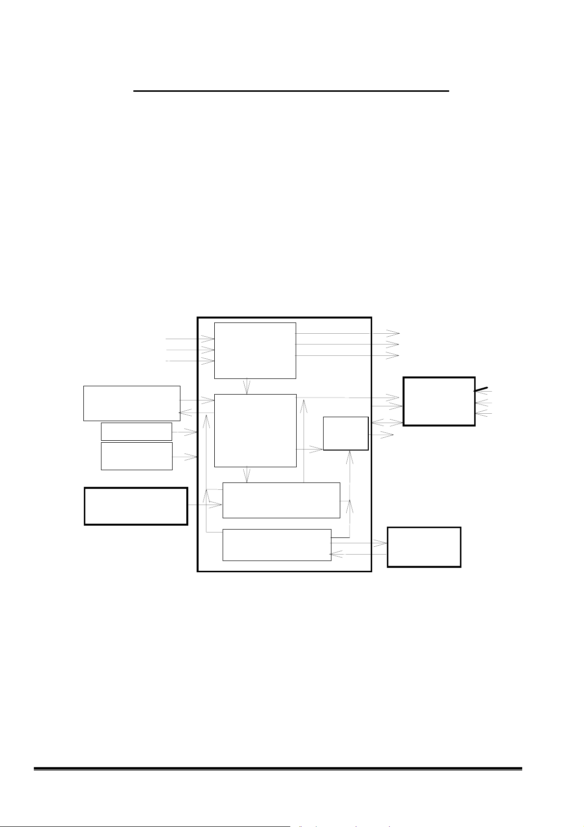
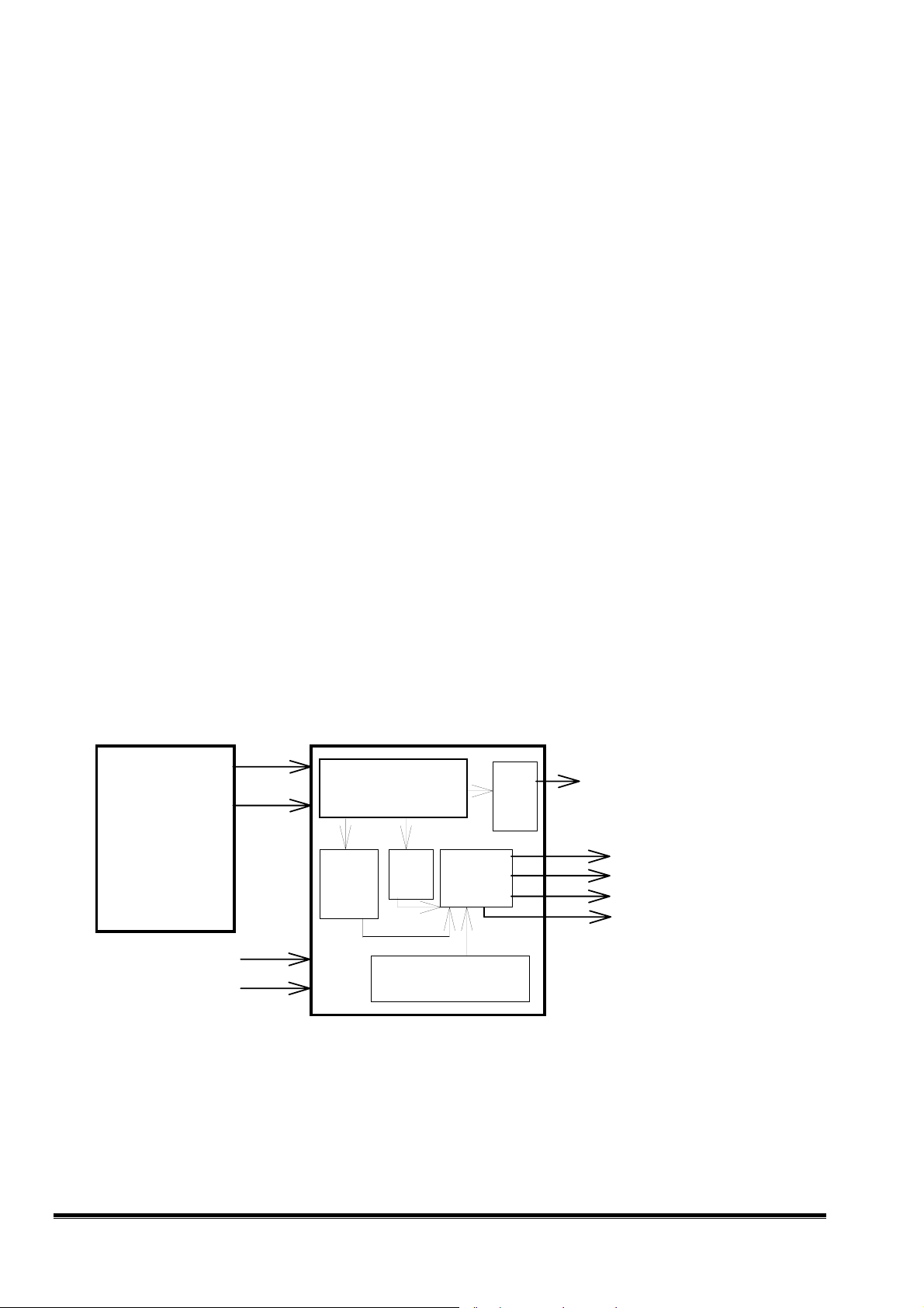
Block diagram :
The major parts of Microcontroller circuit are MCU, EEPROM, OSD IC, and Auto Calibration
Module. The circuit block diagram is shown as below.
MTV112
the
nc &
olarity.
Checking if the
be pressed
function.
ustment
function
PWM
out
ut
Degaussin
Blankin
SC0 - SC2
OSD IC
Display OSD
and out
PWM to video
circuit
To deflection
circuit
PC
RS232
auto ali
nment
ram
ut
Hsync
nc
Vs
H-
olarit
EEPROM
Preset mode
User saved mode
Reset circuit
12MHz Crystal
circuit
Control Panel
5 keys
i-ke
Left,Right,Enter,Ex
MCU
Detectin
in
ut signals
of H,Vs
H-
Searching for
the same saved
mode timin
with the input
nals and
si
et the data.
valid ke
and do ke
UART) External
ad
21
Page 68

MEA 1786FD2 CRT Monitor Service Guide
3.MCU and the peripheral circuit operation theory:
3-1.MCU function:
The MCU is MTV112, it is an 87C51 with PWM output controlled microcontroller, after
power on,the reset circuit output a "High" to "Low" signal(>40mS) and the 12MHz crystal
oscillated circuit working , the MCU begin to manages the following functions,
(1) To detect mode and output proper SC0, SC1 and SC2 to deflection circuit.
(2) To check if there is the same saved mode in the EEPROM and get the data to transfer
into DC voltages by PWM output and RC filter circuits to control the picture, color, contrast
and brightness.
(3) To check if there is the valid key be pressed and do the key function.
(4) To memorize mode timings and any adjustable parameters of the picture into EEPROM.
(5) To output data to OSD IC for making an "on screen display control" menu.
(6) The inner registers and PWM output of MCU can be controlled by the external PC
alignment program.
(7) To calibrate the size, position, and geometry of the picture by pressing i-key. It will be
placed right size and position.
3-2.How to detect mode timing:
Only when the mode timing input is stable, we can adjust the picture and check the
horizontal and vertical sync frequency by the OSD menu, and the mode timing input mean the
horizontal sync signal and the vertical sync signal.
(1) The vertical sync frequency measurement:
We use the base timer, it can generate a count during a fixed time, this fixed time is
12/12MHz and we call it "Time_base", so when the first vertical sync generated, we enable
the base timer,and the next vertical sync generated,we disable the base timer,and we only need
to calculate how many counts are during a vertical sync period. The formula is
Vertical sync frequency
= FV
= 1 / Vertical sync period
= 1 / [ Counts * (Time_base)]
==> Vertical sync frequency = 1000000 / Counts
(2) The horizontal sync frequency measurement:
We use the event counter for calculating how many counts are during a long fixed time,
because the vertical sync period is longer than the horizontal sync period, we can enable the
event counter when the first vertical sync generated and disable the event counter when the
next vertical sync generated, this time,we can get the horizontal sync counts during a vertical
sync period.
The formula is Horizontal sync frequency
= FH
= Horizontal sync counts / Vertical sync period
==> Horizontal sync frequency
= Horizontal sync Counts / Vertical sync period
22
Circuit Operation Theory
Page 69
MEA 1786FD2 CRT Monitor Service Guide
u
3-3.What are the valid key functions for user:
There are Five keys on control panel. They are "i-key, "Left," "Right," "Enter," and
"Exit." The one, i-key, is for auto calibration function, the others are used for OSD
controlling. "Enter" for entering sub-menu of main menu, "Exit" for escaping to main menu
from sub-menu or leaving OSD menu, and "Left," "Right" for adjusting the bar value.
Except the OSD basic key functions, the user can only press "Right" for brightness
adjustment, or "Left" for contrast adjustment.
3-4.How to memorize the timing and adjusted data:
The EEPROM is 24C08, it has 1024 bytes memory size and communicates with MCU
by two wires of I2C bus, one wire is "SCL," the other is "SDA".
The MCU send clock and data to EEPROM to do "Write" function and send clock and
receive data from EEPROM to do "Read" function by these two wires.
We define three parts of storage area. One is for the storage of the factory preset data,
another is for saving user adjusted data, the other is for common settings area where stored
the data of the OSD color temperature settings, contrast and brightness value .
3-5.How to display the OSD menu:
The OSD IC is AP3114/AP315 which is developed by vender, it receives the data of the
OSD fonts and attribute what we want to display on the screen from the MCU by 2 wires of
communication, and exports OSD window data and PWM volume to the VIDEO circuit, the
block diagram is shown as below,
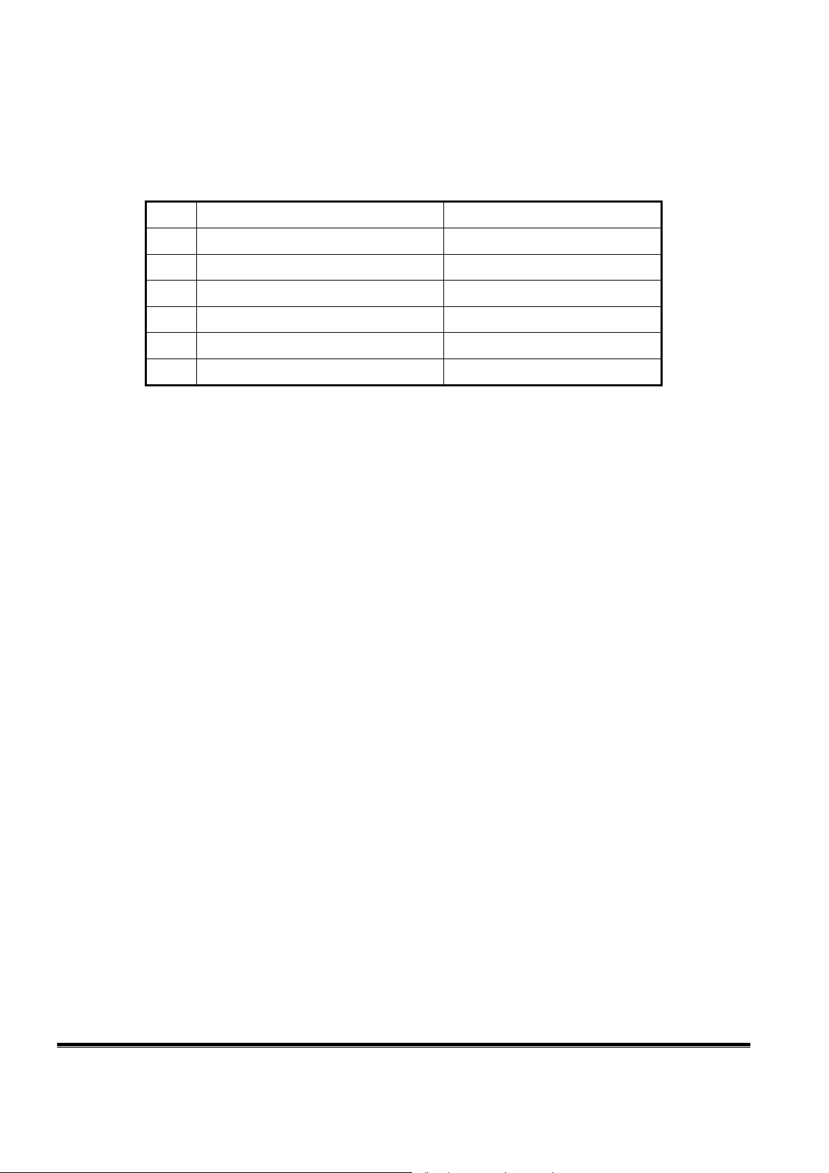
MCU(MTV112)
OSD IC (AP3114)
SDA
(1)Send data to
RAM for OSD
SCL
Shift receiving
register and decoder.
fonts or
attribute.
(2)Send data to
Control
registers
for PWM ouput
Control
register
s
RAM
PWM
output
Fonts
generator
Circuit Operation Theory
Output to
the VIDEO circ
ROUT
GOUT
BOUT
FBKGC
VSYNC
HSYNC
(H-BLANK,HBNK)
3-6.How to execute the auto alignment function:
The MCU MTV112 supports the UART function, it has 2 I/O serious ports, one is the
receiver, the other is the transmitter, they are connected with an interface to PC and PC can
execute alignment program by RS232 communication to send the formatted data to the MCU
for adjusting any adjustable parameters of the picture and saving the adjusted values into
23
VCO circuit
Page 70

MEA 1786FD2 CRT Monitor Service Guide
EEPROM. By this way, we can get the products with the same quality and reduce the
manufacturing time.
Circuit Operation Theory
24
Page 71
MEA 1786FD2 CRT Monitor Service Guide
Alignment Procedure
Preparation for alignment :
(I) Setup unit and keep it warm up at least 30 minutes
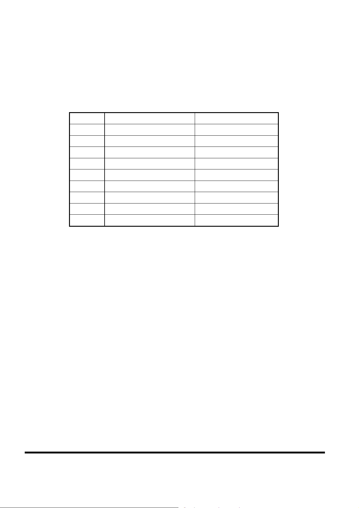
(II) Signal mode
Mode Frequency (H/V) Display
1 31.47k/70Hz (- /+ ) 640 * 400 (VGA400)
2 31.47k/60Hz (- / - ) 640 * 480 (VGA480)
3 53.6 k / 85Hz (+ /+ ) 800 * 600 (SVGA5)
4 60.0 k / 75Hz (+ / + ) 1024 * 768 (UVGA 7)
5 68.6 k/ 85Hz (+/+) 1024 * 768 (UVGA8)
6 79.98k / 75Hz (+/+) 1280 * 1024 (WS7)
1
Page 72

MEA 1786FD2 CRT Monitor Service Guide
Alignment Procedure
1. B﹢Adjustment
a. Input mode 79.98K [WS7] with crosshatch Pattern.
b. Set contrast in OSD to maximal value and brightness in cut off.
c. Adjust main board VR701, let output Voltage : 50 ± 0.2V at D704(near L702).
2. HV Adjustment
a. Input mode 79.98K [WS7] with crosshatch pattern.
b. Adjust VR201to let anode voltage be 26 ± 0.1kV
3. H-size preset :
a. Input mode 31.47K with crosshatch pattern
b. Use OSD to adjust H-size maximum
c. Adjust VR301 to make H-size just over-screen above 16mm
4. Factory setting mode adjustment
1. H-phase : Set picture to the center of screen
2. H-Size : Set picture to 310 ± 2 mm
3. V-center : Set picture to the center of screen
4. V-size : Set picture to 230 ± 2㎜
5. Parallelogram : Set picture to rectangular or balance
6. Trapezoid : Set picture to rectangular or balance of top and bottom
7. Pincushion : Set picture to a real rectangular
8. Tilt : Let top tilt ±1.0mm and bottom tilt ±1.5mm between edge to edge
9. ABL :Let Y=31Ft-L ± 2Ft-L.
2
Page 73

MEA 1786FD2 CRT Monitor Service Guide
Alignment Procedure
5. Focus adjustment
a. Input mode 68.68K [UVGA8] with green crosshatch pattern
b. Adjust V(F2) Focus VR of FBT to make vertical line between center
and corner area of CRT clear
c. Adjust H(F1) to make horizontal line between center and corner area
of CRT clear
d. Repeat step b and c to get the best focus
6. Convergence adjustment
a. Input mode 80K [WS7] with crosshatch patterns
b. Adjust VRs of Yoke and 4-pole , 6-pole to meet specification
7. Color Temperature auto alignment
A. PREPARING ITEMS
a. PC
b. RS232 BOX
c. RS232 CABLE (9P) TO PC
d. RS232 BOX TO MONITOR CABLE (3P)
e. COLOR ANALYZER (CA100)
f. CA100 CABLE TO PC
g. ADJUST PROGRAM (Release NEW Version)
B. Alignment procedure
a. Press "SPACE BAR " to get raster pattern and set contrast and brightness to maximum position,
adjust the G2 VR such that the max. color of R.G.B color bar on the monitor is in the mark region
b. Press "SPACE BAR" to do auto color temperature adjustment and color tracking
C1: 9300K X= 283 ± 15 Y=297 ± 15
C2: 6500K X= 313 ± 15 Y=329 ± 15
c. Press "SPACE BAR" to get full white pattern and set contrast and brightness to maximum position ,
adjust ABL adjustment to let Y = 31ft-l ± 2 ft-l
d. Press "SPACE BAR" to get 3" block and finish the adjustment
3
Page 74
MEA 1786FD2 CRT Monitor Service Guide
Alignment Procedure
8. Clear all of user mode data
After finishing all factory setting , Press enter or exit key to main menu.
Press right or left key to scroll light bar to reset to default and press enter key, then at this time all of user
mode data have been cleared
9. Geometry Specification
ITEM DESCRIPTION SPECIFICATION
1 HORI SIZE 310 ± 2 mm
2 VERT SIZE 230 ± 2 mm
3 SIDE PIN
4 TOP/BOTTOM PIN
5 SIDE BARREL
6 TOP/BOTTOM BARREL
7 TRAPEZOID
8 VIDEO OFFSET
9 PARALLELOGRAM
10. Power Saving Function Check
≦2.0 mm
≦2.0 mm
≦1.5 mm
≦1.5 mm
≦2.0 mm
≦4.0 mm
≦3.5 mm
a. Input mode 31KHz [VGA SIZE] with full white pattern.
b. Press both contrast and brightness keys to maximum position.
c. Remove the horizontal sync signal from input, the unit will go into "Standby" mode.
The picture will disappear, and the LED indicator is amber. The power consumption
should be less than 5W.
d. Remove vertical sync signal from the input, the unit will go into "Suspend" mode. The picture
will disappear, and the LED indicator is amber. The power consumption should be less than 5W.
e. Remove both syncs from input, the unit will go into "Off" mode.
The picture will disappear, and the LED indicator should be amber
The power consumption should be less than 5W in this case.
f. Input H-sync and V-sync signals in case c, d and e, the unit will recover to normal state,
and the LED indicator is green.
g. Disconnect the signal cable from input, the unit will go into "Override" mode.
The raster should be extinguished, and the LED indicator is green. The power
consumption is normal.
h. Re-connect the signal cable in case g, the unit will recover to normal state, and the LED
indicator is green.
4
Page 75

MEA 1786FD2 CRT Monitor Service Guide
Alignment Procedure
11. Eyelet point define
(1). Main board
-C309(*2)
-C612(*2)
-IC202 Heat sink(*2)
-Q602 Heat sink(*2)
-C313(*3)
-L302(*2)
-Q602 “D”(*1)
-L304 pin3, 4(*2)
-M303(*4)
-T301 pin1, 4, 8, 13 and 14(*5)
(2). Video board
-M105 pin5, 9, 11 and focus GND(*4)
12. Touch up point define
(1). Main board
-CN601
-TR602
-IC801 pin1 and pin 21
-IC201 pin 1 and pin 17
-IC202 pin 1 and pin 9
-RL601
-M602
-Q312
-Q302
-D305
-Q318
(2). Video board
-M101 pin 1 and 13
-M102 pin 1 and 11
-M103 pin 1 and 9
5
Page 76
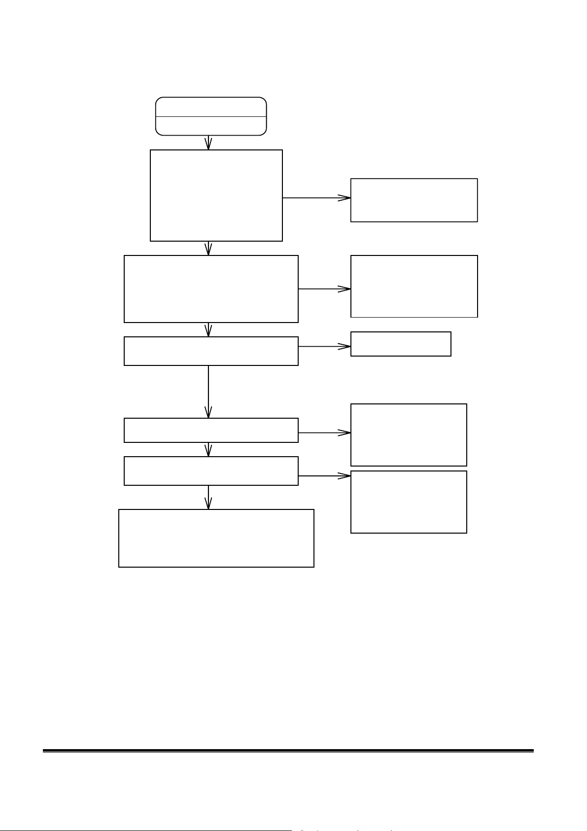
MEA 1786FD2 CRT Monitor Service Guide
Trouble Shooting
Check MCU and OSD for no video output:
Check MCU and OSD
for no video output
Start
Use a preset timing
YES
Check +5V, ok ?
(1) On the Main Board,
(a) IC801 pin40
(b) IC802 pin8
(2) On the Video Board,
IC1901 pin6,19
(OSD IC)
YES
Check F12M=12MHz CLOCK,ok?
(1)On the Main Board
(a) IC801 pin18
(b) Y801 pin1
(2)On the Board, IC1901 pin2,3(OSD IC)
DC level = 1~3V ?
(3)IC1901 pin11 ~ pin18 output PWM ?
YES
Check MCU (IC801)
Reset (pin9) = "H" to "L",ok?
YES
NO
NO
NO
Check +5V power
Check F12M CKT
on the Main Board .
on Main Board,
DC level 1 ~ 3V ?
Check
Reset circuit
Check IC801 (BLANK)= "L",ok?
Check IC802 (EEPROM ),ok?
(1) On the Board
(a) SCL ( IC1901 pin 10)
(b) SDA ( IC1901 pin 9)
YES
YES
NO
NO
Check
(1) "V-FREQ" circuit
(2) "H-FREQ" circuit
(3) IC801 pin 13,15
Check
(1) pin5 (SDA)
(2) pin6 (SCL)
(3) IC802 data
( EEPROM)
(Brightness, Contrast)
1
Page 77
MEA 1786FD2 CRT Monitor Service Guide
Trouble Shooting
Check OSD,MCU for no OSD window:
Check OSD, MCU
for no OSD window
Start
Check +5V, ok?
(1) IC1901(OSD IC) pin,6,19
YES
Check IC1901(OSD IC) pin7(HBNK)&
pin28(V+), ok?
YES
Check SCL, SDA INPUT, ok?
NO
NO
NO
Check +5V power
Check Gnd & +5V
and the R,C CKT
Check HBNK & V+
Check R1906 &
R1907
2.Video board
Caution
destroy the set. There assume that following cases depend on above setup OK. Please follow as below and check it step by step.
Case 1:No video display on screen
•
•
•
•
•
pin6(Blank).
•
•
: Before power on, you must check whether all connectors and components of the set are correct, otherwise it maybe to
Check IC101 pin 10 (Video Contrast). If it is 0 volt, check IC1901 or maybe IC101 pin 10 short.
Check IC101 pin 18,15,13 If they are 0 volts, replace a new IC to IC101.
Check RGB cathode. If anyone pin is 0 volt, replace a new IC to IC102.
Check IC102 output path. It must be right and without short circuit.
Check G1 voltage. If it is lower equal than -182 volts, check spot killer circuit and check IC801
Check CRT heater. If it is dark, check +8v supply voltage of heater.
Replace CRT if it burns out.
2
Page 78
MEA 1786FD2 CRT Monitor Service Guide
Trouble Shooting
Case 2: one or more of R, G, B channel does no display
•
Check IC101 pin 18,15,13. If anyone is 0 volt, replace a new IC to IC101.
•
Check RGB cathode. If anyone pin is 0 volt, replace a new IC to IC102.
•
Check IC102 output path. It must be right and without short circuit.
•
Replace CRT if it burns out.
Case 3: OSD does not display on screen
•
Check IC101 pin 1,19,20. If they are 0 volt, check IC101 and IC1901.
Case 4: No video display on screen, but OSD can display on screen
•
Check IC101 pin 10 (Video Contrast). If it is 0 volt, check IC1901 or maybe IC101 pin 10
short.
Case 5: OSD control cannot adjust Bias
•
Check IC1901.
•
Check DC restore circuit.
Case6: OSD control cannot adjust Drive
•
Check IC101 and IC1901.
Case 7: OSD control cannot adjust Contrast
•
Check IC 101 and IC1901.
Case 8: OSD control cannot adjust Brightness
•
Check brightness control circuit (G1) and IC801 BRITE output.
Case 9: ABL cannot adjust
•
Check ABL circuit.
Case 10: Spot killer function failure
•
Check SG101(300KV spark gap). Replace it if it is inserted error.
•
check spot killer circuit.
Case 11: Picture quality is not so good
•
Check CRT socket. Fix it if it is loose.
•
Check IC101 pin 11(clamp gate). If it has no clamping pulse, check H-clamp pulse switch
circuit.
•
Replace IC102.
Case 12: Moire appears when Y is greater than 18 Ft-l
•
Run auto-alignment procedure to acquire optimum G2 voltage.
•
If necessary, decrease G2 voltage.
Case 13: H-blank function failure
3
Page 79
MEA 1786FD2 CRT Monitor Service Guide
Trouble Shooting
•
Check H-blank circuit
•
Case 14: H-blank phase error
3.NO OUTPUT POWER
NO OUTPUT
Replace F601
D603~D606
Replace
IC601,ZD602
No
No
IC601,ZD602
Check F601
D603~D606
ok?
Yes
Check
ok?
Check
Q602,R607?
Yes
Check
IC601?
Yes
Check
IC603
IC602?
No
No
Replace
Q602,R607
Replace
IC601
Replace
IC603
IC602
Check
FR705,D702
D704,D705?
NoNo
Replace
4
Page 80
MEA 1786FD2 CRT Monitor Service Guide
Trouble Shooting
4. No Raster
CHECK
POWER SUPPLY
CHECK
POWER SAVING
CKT
OK
REPLACE
NG
NG
LED LIGHT
YES
CHECK
Q302
OK
CHECK STEP-UP CKT
Q312, D318
NO RASTER
NO YES
CHECK FR705
=45V
NG
G1 = 0 VDC
REPLACE
NG
HV ABNORMAL
M103 CONNECTOR
LOOSE. (ON V/B)
CHECK G1 VOLTAGE
CHECK IC201
(TDA4856)
OK
CHECK
POWER SUPPLY
5
Page 81
MEA 1786FD2 CRT Monitor Service Guide
Trouble Shooting
5. H.V. ABNORMAL
H.V. ABNORMAL
CORRECT IT!
YES NO
CHECK DRIVER CKT
T302,L301
OK
NG
CHECK C309,C306
YOKE CONNECTOR
LINEAR COIL L304
OK
CHECK FBT PIN2
AT VGA(31K) ABOUT
63V ?
NG
REPLACE
NG
CHECK
Q312,D318
CHECK IC201
OK
CHECK FBT(T301)
OK
6
Page 82
MEA 1786FD2 CRT Monitor Service Guide
NO
Trouble Shooting
6. CHECK IC201(TDA4856)
DEFLECTION OUTPUT
ABNORMAL
OK
CHECK
Q301,Q310,Q311
Q201
OK
CHECK OUTPUT
STAGE
CHECK PIN6,PIN8
OUTPUT
(FREQ & DUTY)
NG
REPLACE
YES
CHECK PIN30
>4.4V ?
CHECK
R215,R214
C210
NG
REPLACE
IC201
NG
YES
YES
CHECK FBT(T301)
CHECK PIN10(VCC)
=12V ?
NO
CHECK
R251,R253
R249,C216
NG
REPLACE
OK
YES
CHECK
SUSPEND SIGNAL
="HIGH"
NG
CHECK
Q702
NO
OK
NO
CHECK +14V
YES
CHECK Q701
EMITTER
=14V
YES
CHECK
Q702
Q701
OK
CHECK +14V
TRACE SHORT?
CHECK
POWER SUPPLY
NG
REPLACE
CHECK
POWER SUPPLY
REPLACE
SHORT
COMPONENTS
7
Page 83
MEA 1786FD2 CRT Monitor Service Guide
Trouble Shooting
7. PINCUSHION NG
TRAPEZOID NG
UNBALANCE NG
PARALLEGRAM NG
H-PHASE NG
GEOMETRIC FUNCTION NG
CHECK MCU,IF OK REPLACE IC201
V-CENTER NG
8. NO VERTICAL OUTPUT &
RETRACE LINE NO BLANKING
NO VERTICAL OUTPUT
CHECK B+ CORRECT ?
PIN 3(+14V) &
PIN 7(+45V)
YES
CHECK IC201 (TDA4856)
PIN12 PIN13 OUTPUT
CORRECT ?
NO
REPLACE
IC201
(TDA4856)
YES
CHECK
R275,R274
IF PIN3 FAILS CHECK FR223
NO
IF PIN7 FAILS CHECK +45V &
FR234
OK
REPLACE
IC202
(TDA4866)
OK
NG
NG
REPLACE
NO VERTICAL BLANKING
CHECK IC202(TDA4866)
PIN8 OUTPUT CORRECT?
CHECK
IC201(TDA4856)
PIN16 OUTPUT
CORRECT ?
CHECK
NG
R254,C223,Q202,R239,
R232
OK
YES
NG
REPLACE
IC202
(TDA4866)
NG
REPLACE
IC201
(TDA4856)
8
Page 84
MEA 1786FD2 CRT Monitor Service Guide
NG
Trouble Shooting
9. SPOT KILLER NG
SPOT KILLER NG
CHECK -190V
CHECK BLANK SIGNAL
UC CKT
CHECK Q203 CIRCUIT
OK
CHECK CONNECTOR
G1 VOLTAGE
G1=0
CHECK
Q202
CHECK
R216,R217,R218
HOLDDOWN CKT
YES
NO
CHECK -190V TRACE
G1< -50VDC
NG
REPLACE
OKOK
CHECK G1 VOLTAGE
IF IT BECOMES
VERY LOW (LESS THAN
-120VDC) WHEN POWER
SWITCH OFF.
YES
CHECK Q202
9
Page 85
MEA 1786FD2 CRT Monitor Service Guide
Trouble Shooting
10. FOCUS NG
FOCUS NG
NG
CHECK IC201 PIN32
WAVEFORM
OK
CHECK FOCUS TRACE CHECK H-PARA SIGNAL
OK
REPLACE
IC201
NG
REPLACE
NG
C329,R327
NG
REPLACE
OK
CHECK CS-1,CS-2
SIGNAL FOIL
TRACE
OK
CHECK Q321 FOCUS
CKT
NG
REPLACE
COMPONENT
10
Page 86
MEA 1786FD2 CRT Monitor Service Guide
Trouble Shooting
11. HORIZONTAL SIZE CAN NOT CONTROL
HORIZONTAL SIZE CAN NOT CONTROL
CHECK Q314,Q315,Q316 REPLACE
CHECK Q317,Q318
YES
CHECK IC201
PIN11 ABOUT
para wave
CHECK +12V
REPLACE
NO
YES
NO
REPLACE
12.BRIGHTNESS CAN NOT CONTROL
NG
YES
CHECK UC CIRCUIT
BRIGHTNESS
CAN NOT
CONTROL
CHECK BRITE SIGNAL
ADJUSTABLE
YES
CHECK C224,Q202
R241,Q203,R232
R231,+48V,+8V
NO
REPLACE
CHECK UC CIRCUIT
11
Page 87
MEA 1786FD2 CRT Monitor Service Guide
Trouble Shooting
13. SIZE REGULATION NG
SIZE REGULATION NG
H SIZE
REGULATION NG
CHECK ABL CIRCUIT
FROM FBT PIN 8
R330
V SIZE
MAIN BOARD
OK
CHECK ABL CIRCUIT
REGULATION NG
REPLACE R329
R258,R211
14.Unstable Vertical Display
Unstable Vertical Display
H & V SIZE
REGULATION NG
H.V. ABNORMAL
H.V.
OK
REPLACE FBT
CHECK REGULATION CIRCUIT
R329,C324,R330,HMOD,VMOD
CKT
REPLACE THE FAILURE
COMPONENTS
N Y
IC201 pin 24
sawtooth genentor
Check IC201
NY
& Ambient
CKT
Check IC202
& Ambient
CKT
IC 202
has output
Check DY
12
Page 88
MEA 1786FD2 CRT Monitor Service Guide
Trouble Shooting
15. No Blanking
No Blanking
IC801 pin 6
has output
Check Q202
& Ambient
CKT
Trace open.
13
Page 89
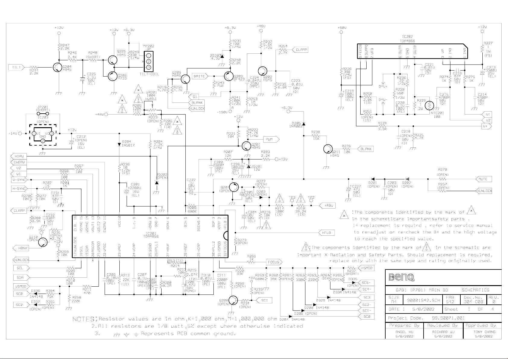
Diamond View 1786FD2 (Main) (1 of 4)
Page 90
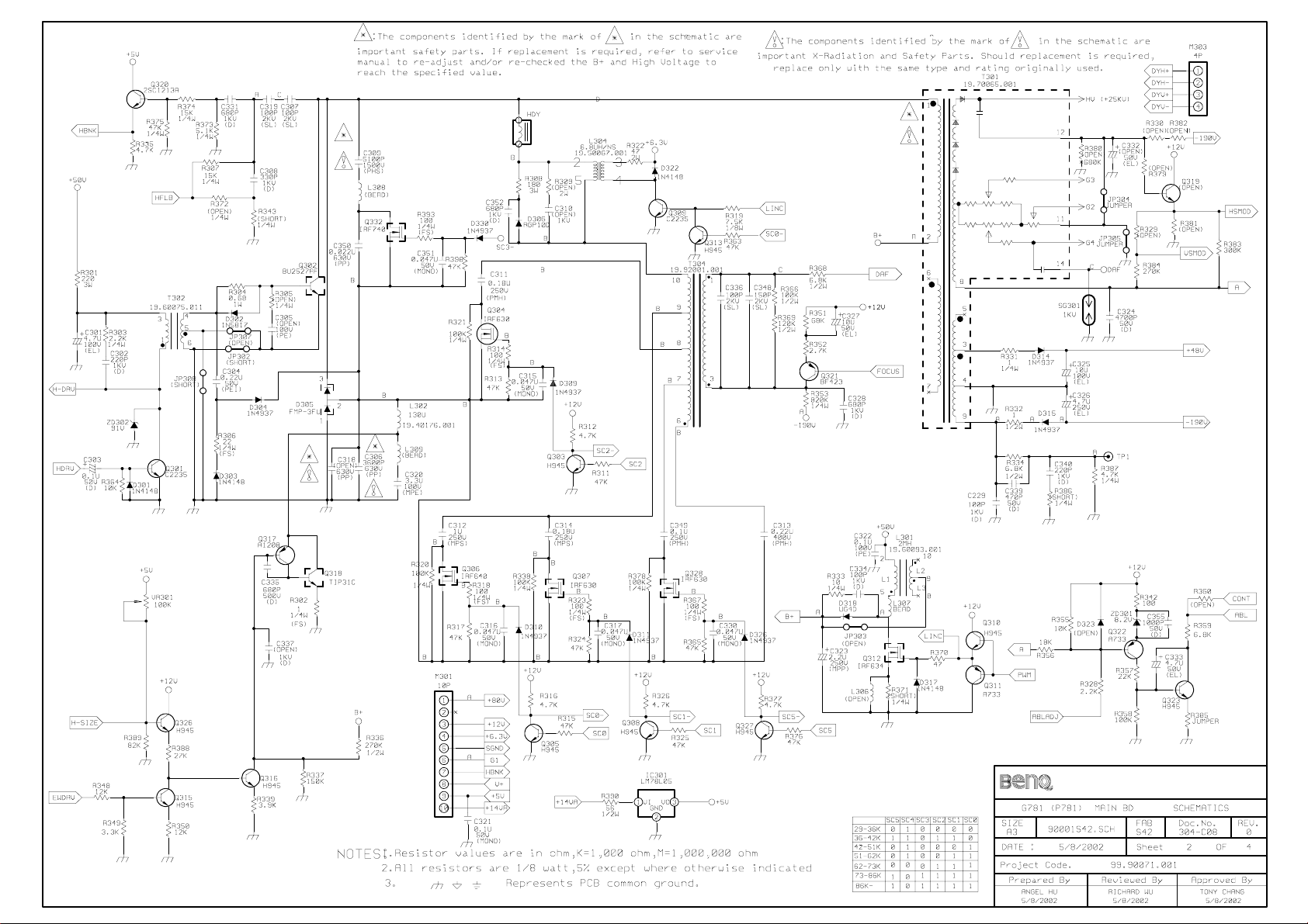
Diamond View 1786FD2 (main) (2 of 4)
Page 91
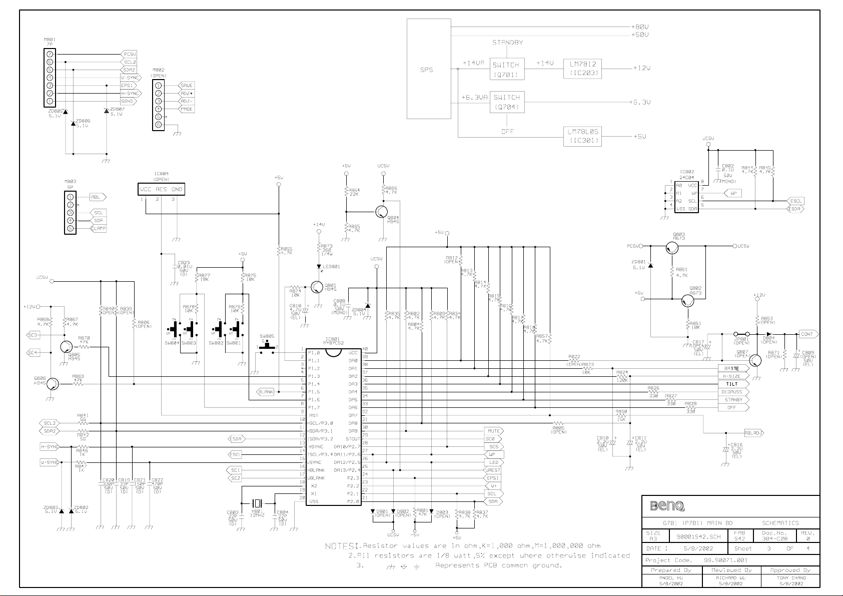
Diamond View 1786FD2 (main) (3 of 4)
Page 92
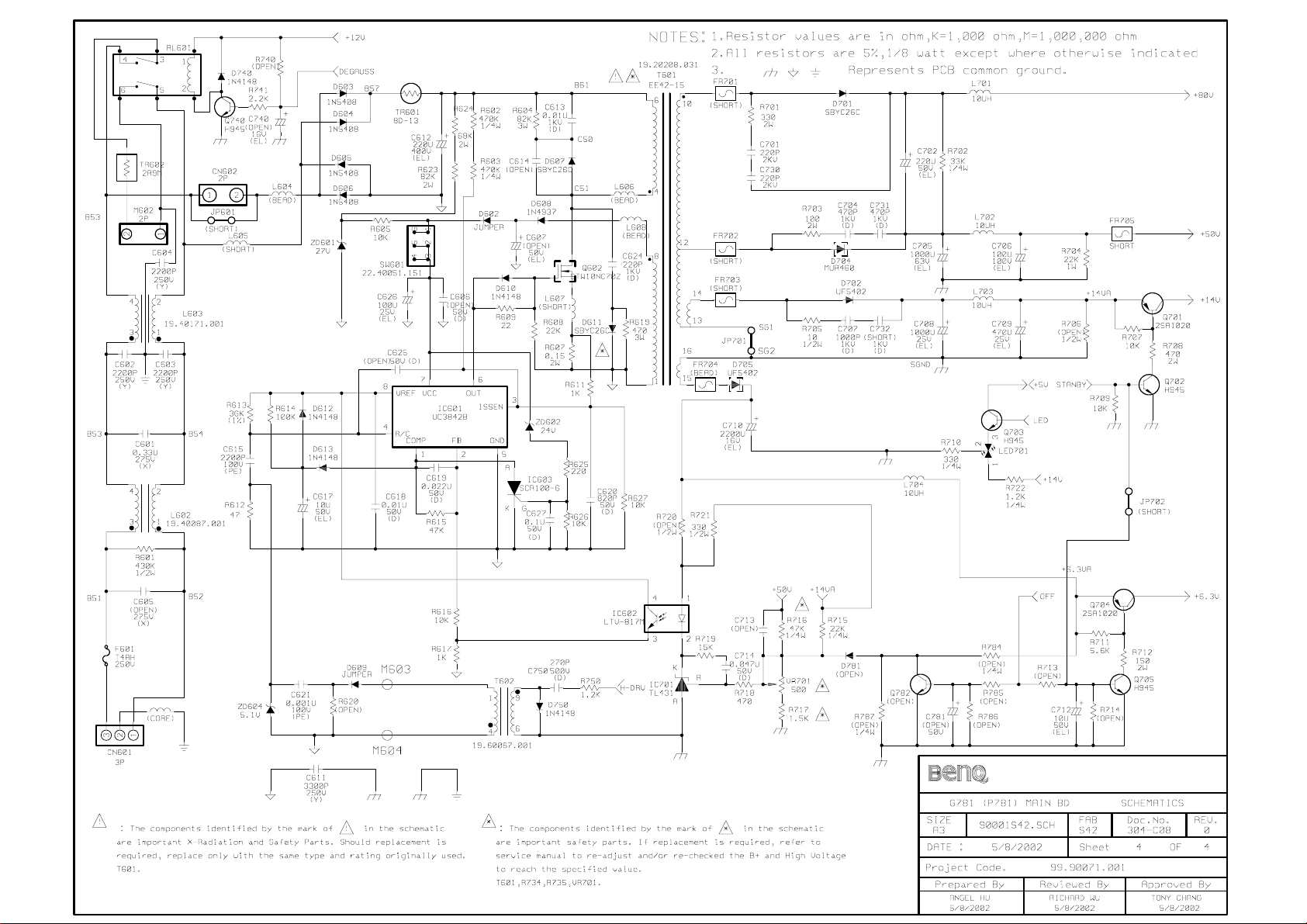
Diamond View 1786FD2 (Main) (4 of 4)
Page 93
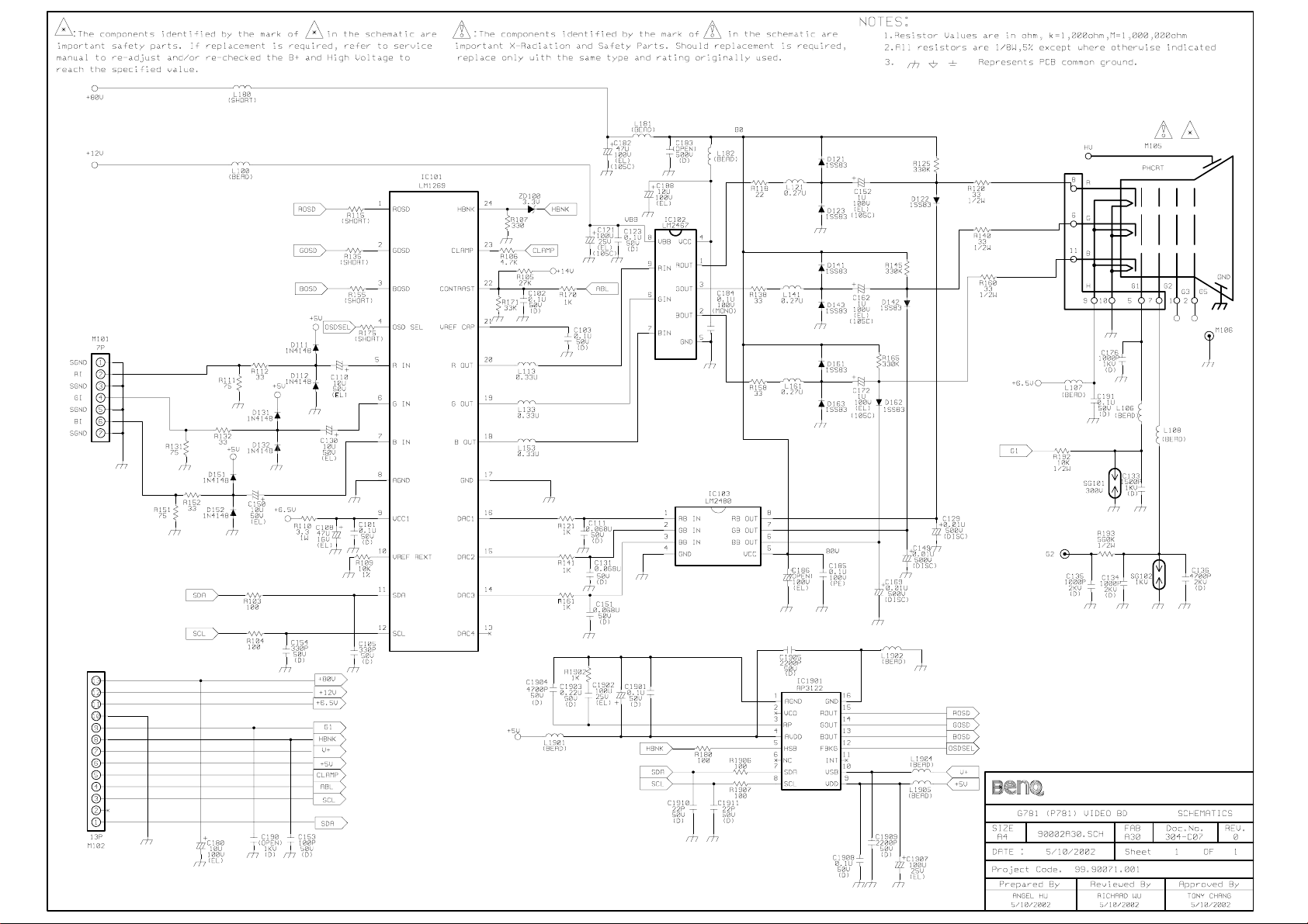
Diamond View 1786FD2 Video PCB
Page 94
Diamond View 1786FD2 Video PCB
 Loading...