

Page 1

Acer AT2645 & AT2646
Service Guide
1
Page 2

Service Guide Version and Revision
Version Date Revision History TPV Model Name
A00 May-15-08 Initial release E268M2NBWAZEN
2
Page 3
Copyright
Copyright 2003 Acer Technology Corp.
All rights reserved.
This manual may not, in whole or in part, be copied, photocopied, reproduced, translated, or converted to any
electronic machine readable form without prior written permission of Acer Technology Corp.
ACER AT2645 & AT2646 Service Manual.
Printed in Fujian.
Disclaimer
The information in this guide is subject to change without notice. Acer Incorporated makes no representations or
warranties, either expressed or implied, with respect to the contents hereof and spe cifically disclaims any warranties
of merchantability or fitness for any particular purpose. Any Acer Incorporated software described in this manual is
sold or licensed "as is". Should the programs prove defective following their purchase, the buyer (and not Acer
Incorporated, its distributor, or its dealer) assumes the entire cost of all necessary servicing, repair, and any
incidental or consequential damages resulting from any defect in the software.
Acer is a registered trademark of Acer Corporation.
Intel is a registered trademark of Intel Corporation.
Pentium and Pentium II/III are trademarks of Intel Corporation.
Other brand and product names are trademarks and/or registered trademarks of their respective holders.
Trademarks
All other trademarks are property of their respective owners.
Conventions
The following conventions are used in this manual:
Screen messages Denotes actual messages that appear on screen.
NOTE Gives bits and pieces of additional information related to the current topic.
WARNING Alerts you to any damage that might result from doing or not doing specific
actions.
CAUTION Gives precautionary measures to avoid possible hardware or software
problems.
IMPORTANT Remind you to do specific actions relevant to the accomplishment of
procedures.
3
Page 4

Preface
Before using this information and the product it supports, please read the following general information.
1. This Service Guide provides you with all technical information relating to the BASIC CONFIGURATION decided
for Acer's "global" product offering. To better fit local market requirements and enhance product competitiveness,
your regional office may have decided to extend the functionality of a machine (e.g. add-on card, modem, or extra
memory capability). These LOCALIZED FEATURES will NOT be covered in this generic service guide. In such
cases, please contact your regional offices or the responsible personnel/channel to provide you with further
technical details.
2. Please note WHEN ORDERING FRU PARTS, that you should check the most up-to-dat e information available on
your regional web or channel. If, for whatever reason, a part number change is made, it will not be noted in the
printed Service Guide. For ACER-AUTHORIZED SERVICE PROVIDERS, your Acer office may have a
DIFFERENT part number code to those given in the FRU list of this printed Service Guide. You MUST use the list
provided by your regional Acer office to order FRU parts for repair and service of customer machines.
Warning: (For FCC Certified Models)
Note: This equipment has been tested and found to comply with the limits for a Class B digital device, pursuant to
Part 15 of the FCC Rules. These limits are designed to provide reasonable protection against harmful interferen ce in
a residential installation. This equipment generates, uses and can radiate radio frequency energy, and if not installed
and used in accordance with the instructions, may cause harmful interference to radio communications. However,
there is no guarantee that interference will not occur in a pa rticular i nstallation. If this equipment does cause harmful
interference to radio or television reception, which can be determined by turning the equipment off and on, the user
is encouraged to try to correct the interference by one or more of the following measures:
1. Reorient or relocate the receiving antenna.
2. Increase the separation between the equipment and receiver.
3. Connect the equipment into an outlet on a circuit different from that to which the receiver is connected.
4. Consult the dealer or an experienced radio/TV technician for help.
Notice:
1. The changes or modifications not expressly approved by the party responsible for compliance could void the
user's authority to operate the equipment.
2. Shielded interface cables and AC power cord, if any, must be used in order to comply with the emission limits.
3. The manufacturer is not responsible for any radio or TV interference caused by unauthorized modification to this
equipment. It is the responsibility of the user to correct such interference.
As ENERGY STAR
®
Partner our company has determined that this product meets the ENERGY STAR
guidelines for energy efficiency.
®
Warning:
To prevent fire or shock hazard, do not expose the monitor to rain or moisture. Dangerous high voltages are
present inside the monitor. Do not open the cabinet. Refer servicing to qualified personnel only.
4
Page 5

Precautions
z Do not use the monitor near water, e.g. near a bathtub, washbowl, kitchen sink, laundry tub, swimming pool or in
a wet basement.
z Do not place the monitor on an unstable trolley, stand, or table. If the monitor falls, it can injure a person and
cause serious damage to the appliance. Use only a trolley or stand recommended by the manufacturer or sold
with the monitor. If you mount the monitor on a wall or shelf, uses a mounting kit approved by the manufacturer
and follow the kit instructions.
z Slots and openings in the back and bottom of the cabinet are provided for ventilation. To ensure reliable
operation of the monitor and to protect it from overheating, be sure these openings are not blocked or covered.
Do not place the monitor on a bed, sofa, rug, or similar surface. Do not place the monitor near or over a radiator
or heat register. Do not place the monitor in a bookcase or cabinet unless proper ventilation is provided.
z The monitor should be operated only from the type of power source indicated on the label. If you are not sure of
the type of power supplied to your home, consult your dealer or local power company.
z The monitor is equipped with a three-pronged grounded plu g, a plug with a third (groun ding) pin. This plug will fit
only into a grounded power outlet as a safety feature. If your outlet does not accommodate the three-wire plug,
have an electrician install the correct outlet, or use an adapter to ground the appliance safely. Do not defeat the
safety purpose of the grounded plug.
z Unplug the unit during a lightning storm or when it will not be used for long periods of time. This will protect the
monitor from damage due to power surges.
z Do not overload power strips and extension cords. Overloading can result in fire or electric shock.
z Never push any object into the slot on the monitor cabinet. It could short circuit parts causing a fire or electric
shock. Never spill liquids on the monitor.
z Do not attempt to service the monitor yourself; opening or removing covers can expose you to dangerous
voltages and other hazards. Please refer all servicing to qualified service personnel
z To ensure satisfactory operation, use the monitor only with UL listed computers which have appropriate
configured receptacles marked between 100 - 240V AC, Min. 5A.
z The wall socket shall be installed near the equipment and shall be easily accessible.
Special Notes On LCD TV Monitors
The following symptoms are normal with LCD TV monitor and do n ot indicate a problem.
Notes
z Due to the nature of the fluorescent light, the screen may flicker during initial use. Turn off the Power Switch and
then turn it on again to make sure the flicker disappears.
z You may find slightly uneven brightness on the screen depending on the desktop pattern you use.
z The LCD TV screen has effective pixels of 99.99% or more. It may include blemishes of 0.01% or less such as a
missing pixel or a pixel lit all of the time.
z Due to the nature of the LCD TV screen, an afterimage of the previous screen may remain after switching the
image, when the same image is displayed for hours. In this case, the screen is recovered slowly by changing the
image or turning off the Power Switch for hours.
5
Page 6

Table Of Contents
Monitor Features
General Specifications ……………………………………… 7
LCD TV Description ……………………………………… 9
Chapter 1
Chapter 2
Chapter 3
Chapter 4 Machine Disassembly
Precautions And Notices ……………………………………… 9
D-SUB PIN Distribution ……………………………………… 10
Factory Preset Display Modes ……………………………………… 11
LCD TV Panel Specification ……………………………………… 12
Panel Features ……………………………………… 12
General Specifications ……………………………………… 12
Mechanical Specifications ……………………………………… 12
Optical Specifications ……………………………………… 13
Connecting Peripherals
Front Panel Controls ………………………………………….. 14
Remote Control & OSD Operating
Instructions
Using The Remote Control ……………………………………… 15
Using The OSD Menus 17
LOGO ……………………………………… 25
……………………………………… 7
……………………………………… 14
…………………………………………………. 15
……………………………………… 26
Chapter 5 Trouble Shooting
Chapter 6 Upgrade Firmware
Chapter 7 White-Balance, Luminance Adjustment
FRU (Field Replaceable Unit) List
Chapter 8
Chapter 9 PCB Layout
Chapter 10 Schematic Diagram
Exploded Diagram ……………………………………… 43
EDID Data ……………………………………… 44
……………………………………… 31
……………………………………… 35
……………………………………… 40
……………………………………… 43
……………………………………… 45
……………………………………… 49
6
Page 7
Monitor Features
Chapter 1
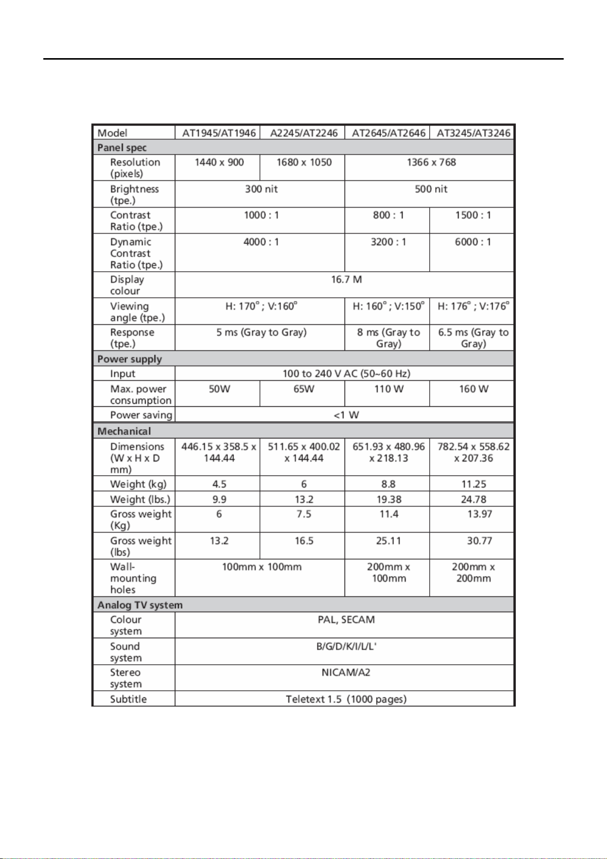
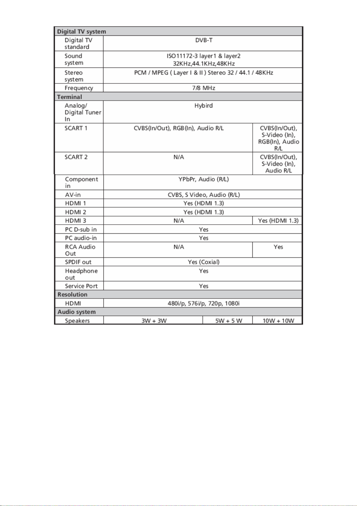
General Specifications
7
Page 8
8
Page 9

LCD TV Description
The LCD TV will contain a main board (include audio), a switching power board, a function keyboard, an IR Board
and a side board. The main board and power board will house the flat panel to control logic I2C bus, DDC,
brightness control logic for LCD panel, DC-DC conversion to supply the appropriate power to the whole board and
transmitting TTL level signals into LCD Module to drive the LCD display circuit.
The inverter board will drive the five CCFLs (Cold Cathode Fluorescent Lamp).
The switching power board will provides the power ON/OFF to control the TV and control LED indicator for DPMS.
The function keyboard and Remote Control will provide the OSD control signal to the Main Board.
Precautions And Notices
1-1 Assembly Precaution
(1) Please do not press or scratch LCD panel surface with anything hard. And do not soil LCD panel surfa ce
by touching with bare hands (Polarize film, surface of LCD panel is easy to be flawed)
In the LCD panel, the gap between two glass plates is kept perfectly even to maintain display
characteristic and reliability. If this panel is subject to hard pressing, the following occurs :
(a) Uniform color (b) Orientation of liquid crystal becomes disorder
(2) Please wipe out LCD panel surface with absorbent cotton or soft cloth in case of it bein g soiled.
(3) Please wipe out drops of adhesive like saliva and water in LCD panel surface immediately.
They might damage to cause panel surface variation and color change.
(4) Do not apply any strong mechanical shock to the LCD panel.
1-2 Operating Precaution
(1) Please be sure to unplug the power cord before remove the back-cover. (be sure the power is turn-off)
(2) Please do not change variable resistance settings in MAIN-BOARD; they are adju sted to the most suitable
value. If they are changed, it might happen LUMINANCE does not satisfy the white balance spec.
(3) Please consider that LCD backlight takes longer time to become stable of radiation characteristic in low
temperature than in room temperature.
(4) Please pay attention to displaying the same pattern for very long-time. Image might stick on LCD.
1-3 Storage Precaution
(1) When you store LCD for a long time, it is recommended to keep the temperature between -20°C - 60°C
without the exposure of sunlight and to keep the humidity less than 85% RH.
(2) Please do not leave the LCD in the environment of high humidity and high temperature such as 60°C,
95%RH.
(3) Please do not operate the LCD in the environment of abnormal temperature, below 0°C.
1- 4 High Voltage Warning
The high voltage was only generated by Power support part, if carelessly conta cted the transformer on this
module, can cause a serious shock.
9
Page 10
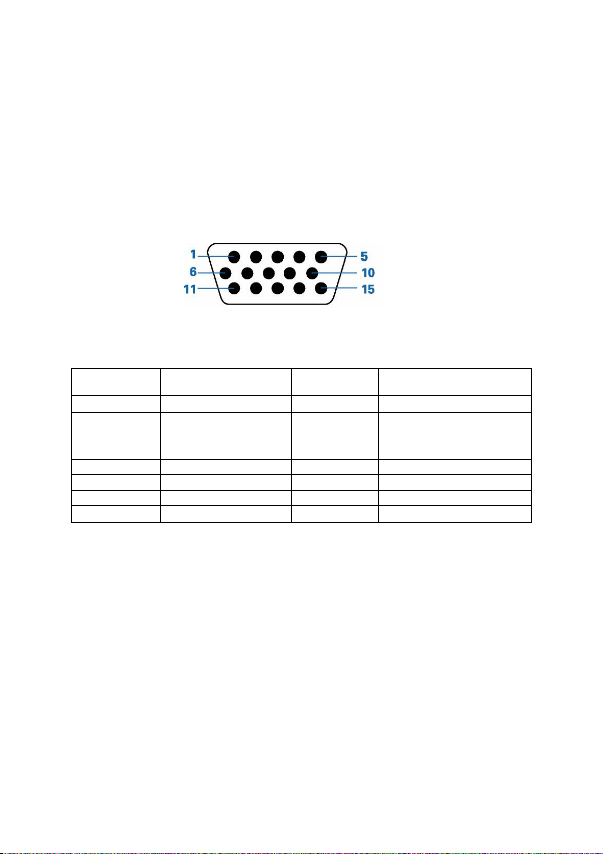
D-SUB PIN Distribution
This procedure gives you instructions for installing and using the LCD TV display.
(1) Position the display on the desired operation and plug the power cord into a convenient AC outlet. Three-wire
power cord must be shielded and is provided as a safety precaution as it connects the chassis and cabinet to
the electrical conduct ground. If the AC outlet in your location does not have provisions for the grounded type
plug, the installer should attach the proper adapter to ensure a safe ground potential.
(2) Connect the 15-pin color display shielded signal cable to your signal system device and lock both screws on the
connector to ensure firm grounding. The connector information is as follow:
15 - Pin Color Display Signal Cable
Pin NO. Description Pin NO. Description
1 Red video input 9 DDC +3.3V (or 5V)
2 Green video input /SOG 10 Logic ground
3 Blue video input 11 GND
4 GND 12 Serial data line (SDA)
5 GND– cable detect 13 H. Sync / H+V
6 Red video ground 14 V. Sync
7 Green video ground 15 Data clock line (SCL)
8 Blue video ground
10
Page 11
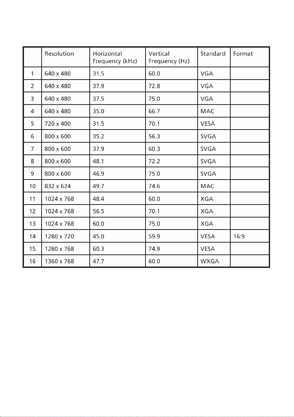
Factory Preset Display Modes:
VGA/HDMI Input Signal Reference Chart
11
Page 12
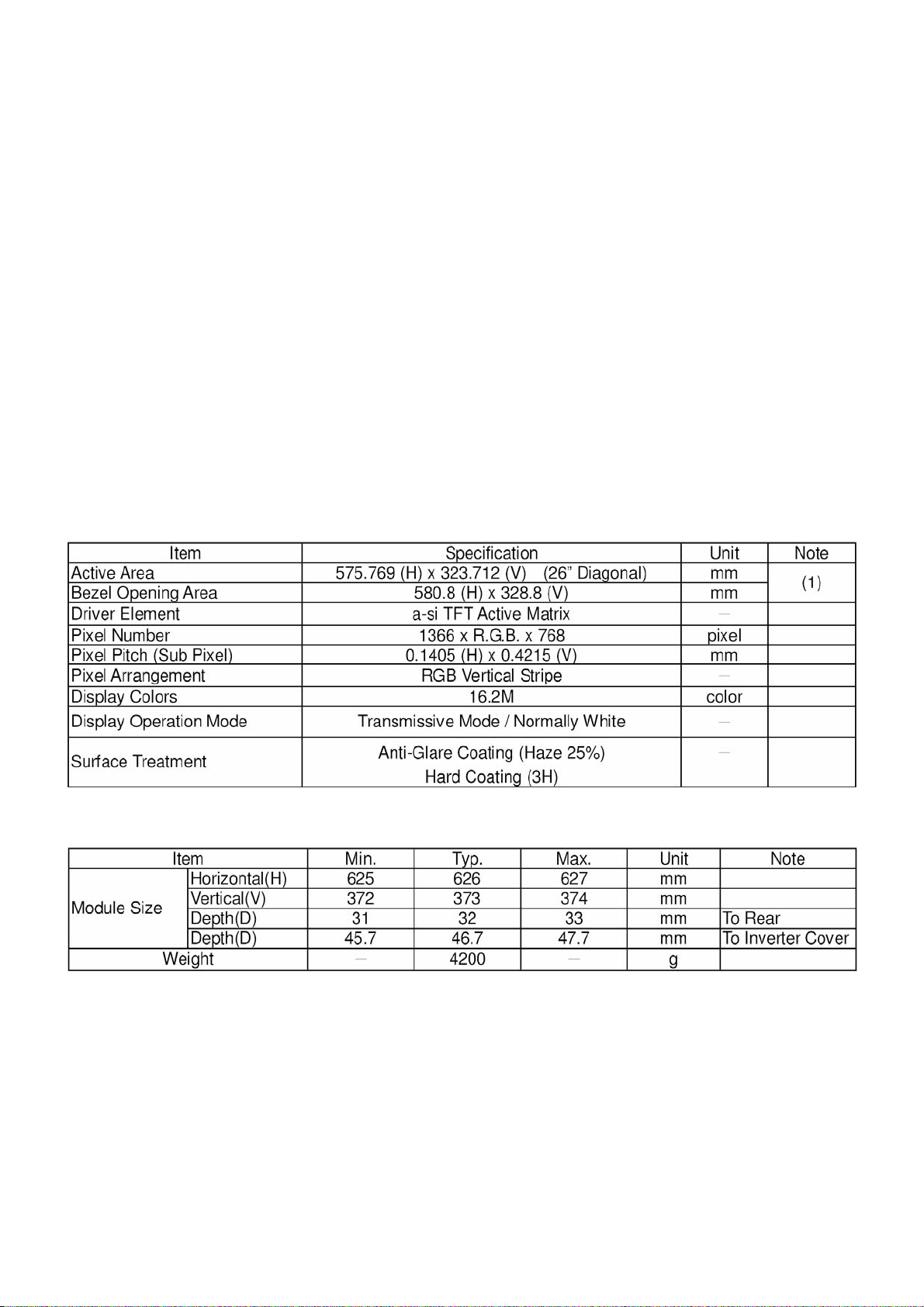
LCD TV Panel Specification
V260B1- L11 is a TFT Liquid Crystal Display module with 5U-CCFL Backlight unit and 1ch-LVDS interface. The
display diagonal is 26”. This module supports 1366 x 768 WXGA format and can display 16.2M colors (6-bit+FRC
colors). The inverter module for backlight is built-in.
Panel Features
- Excellent Brightness 500nits
- Contrast Ratio (800:1)
- Fast Response Time (8ms)
- Color Saturation NTSC 72%
- WXGA (1366 x 768 pixels) Resolution
- DE (Data Enable) Only Mode
- LVDS (Low Voltage Differential Signaling) Interface
- Viewing Angle: 160(H)/150(V) (CR>10) TN Technology
-Color Reproduction (Nature Color)
General Specifications
Mechanical Specification
12
Page 13
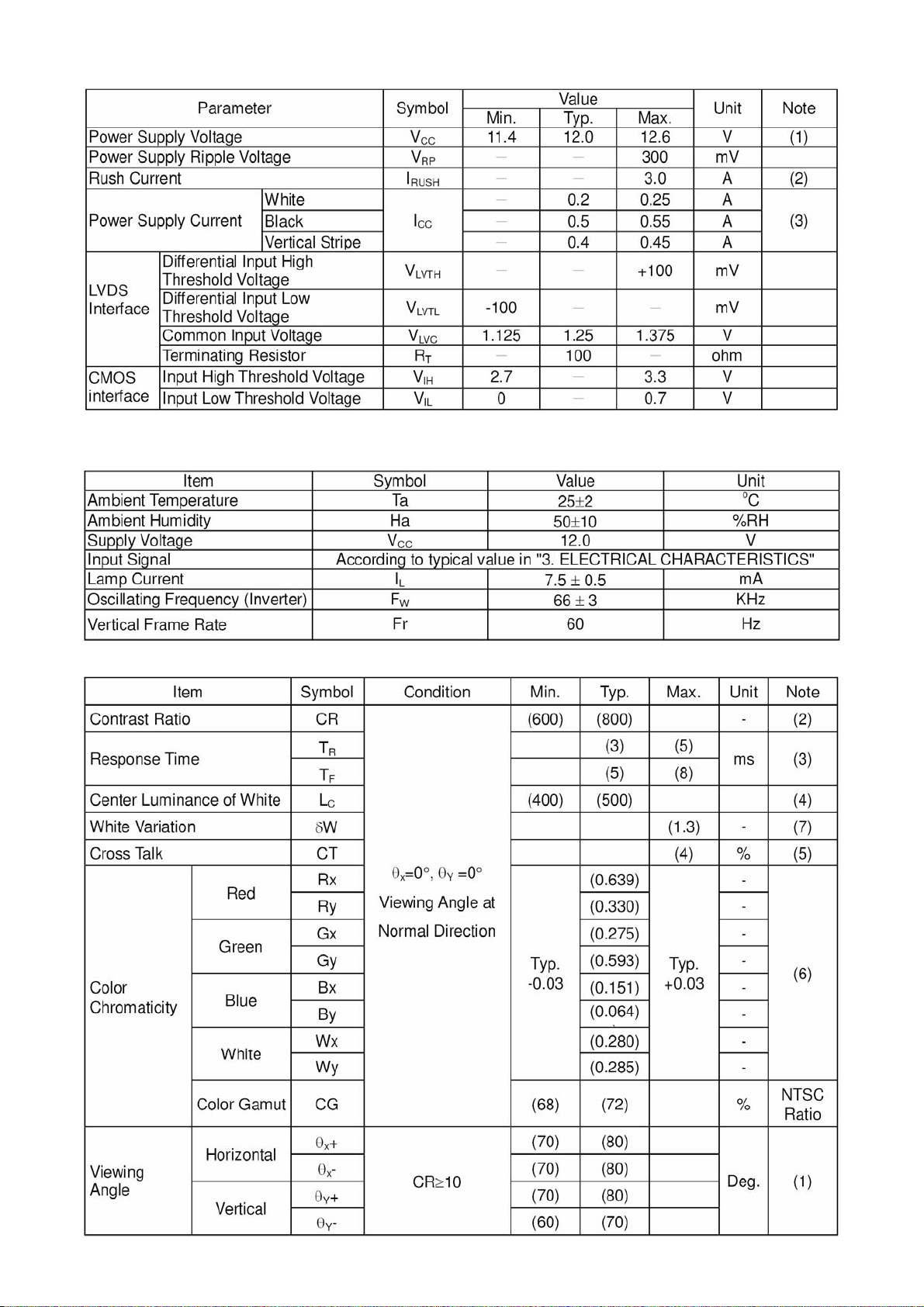
Electrical Characteristics
Optical Specifications
Test Conditions
Optical Specifications
13
Page 14
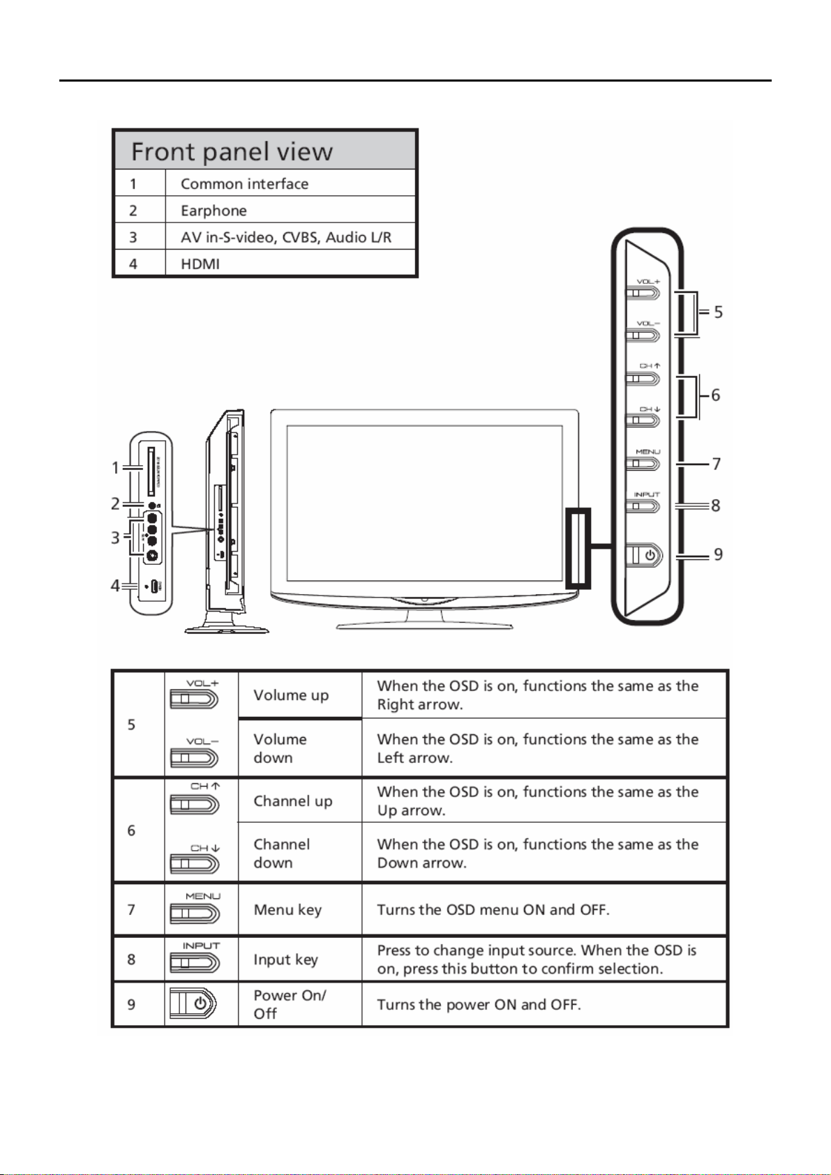
Connecting Peripherals
Front panel controls
Chapter 2
14
Page 15
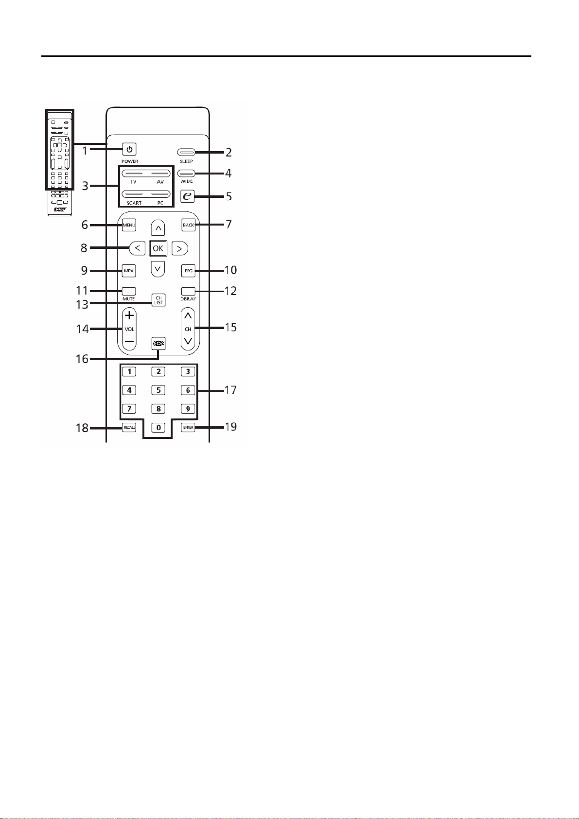
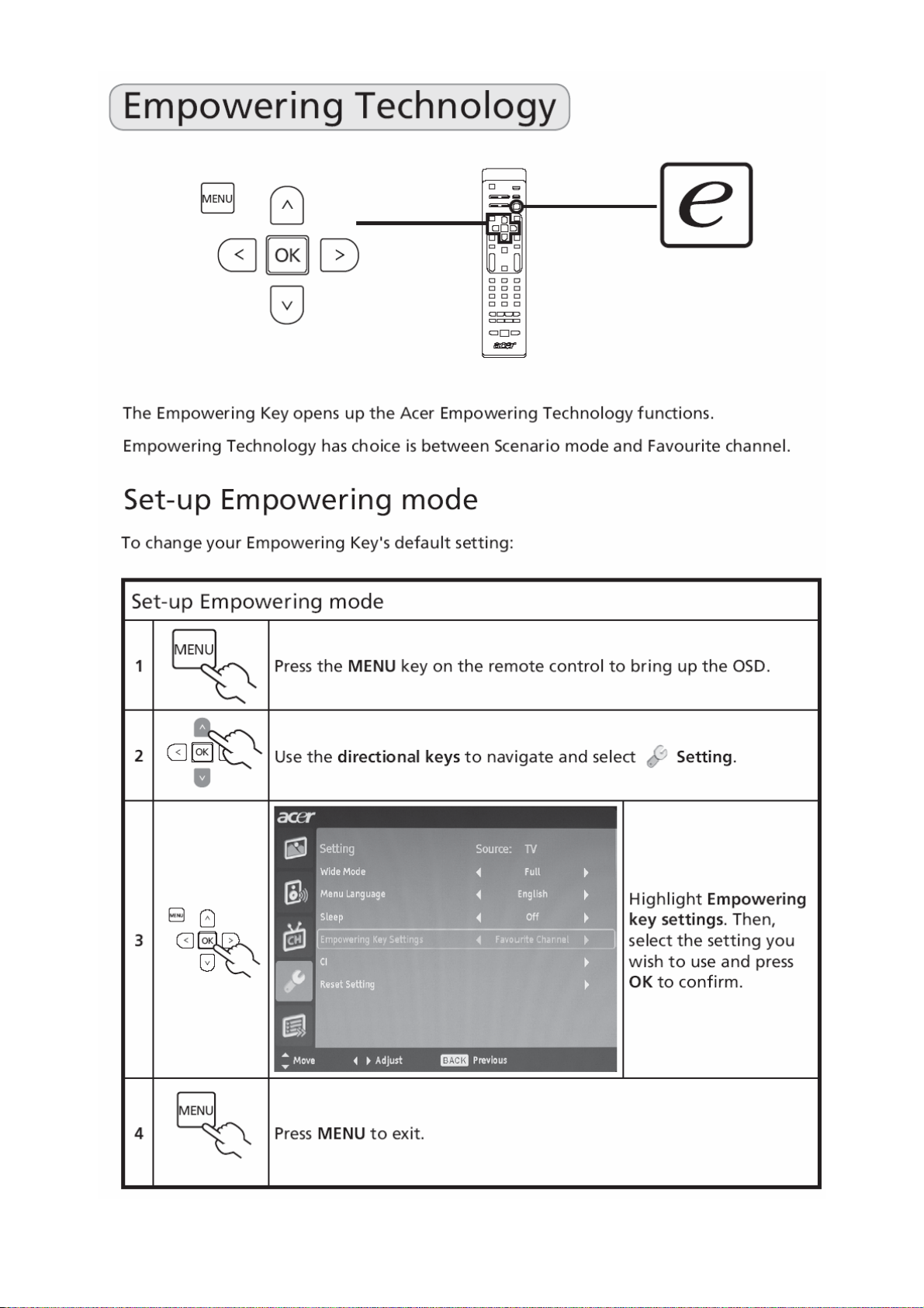
Remote Control & OSD Operating instructions
Chapter 3
Using the Remote Control
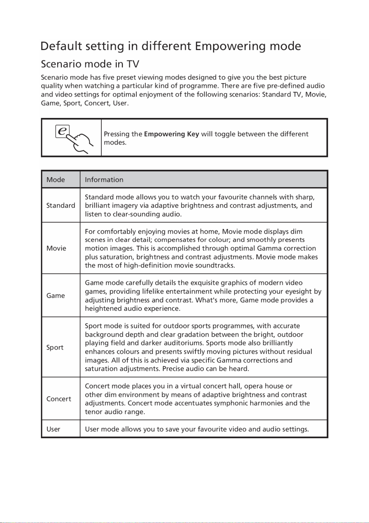
5 e (Empowering Technology)
Press to activate Acer Empowering
Technology.
6 MENU
Press to open or close the Menu.
7 Back
Press to back to previous Menu.
8 Directional keys/OK
9 MPX
Press to select the audio type,
displayed in the top right-hand
corner(mono, stereo, bilingual).
10 EPG
Press to launch Electronic Programme
Guide (EPG) mode
(Digital TV mode only).
11 MUTE
Press to toggle audio on and off.
12 DISPLAY
Press to display or change input/
channel information (dependent on
input/source type).
13 CH LIST
.
1 POWER
Press to turn your TV on/off.
2 SLEEP
Press to set a time period after which
the TV will switch itself to standby
(5, 30, 45, 60, 90 or 20 minutes).
3 Input buttons (TV/AV/SCART/PC)
Press to select correct input mode.
4 WIDE
Press to toggle scaling mode
between Wide detect, 4:3, 6:9,
Full*, Panorama and Letterbox , 2, 3
modes.
Press to launch the channel list. See
page 40.
14 VOL (+/-)
Press to increase or decrease the
volume.
15 CH (up/down)
Press to sequentially select the TV
channel.
16 Sound
Press to turn audio mode to Surround
mode.
17 Number keys.
18 RECALL
Press to return to the previous channel.
19 ENTER
Press to confirm channel number
selection.
PS: The 26" and 32" models does not support Full mode.
15
Page 16
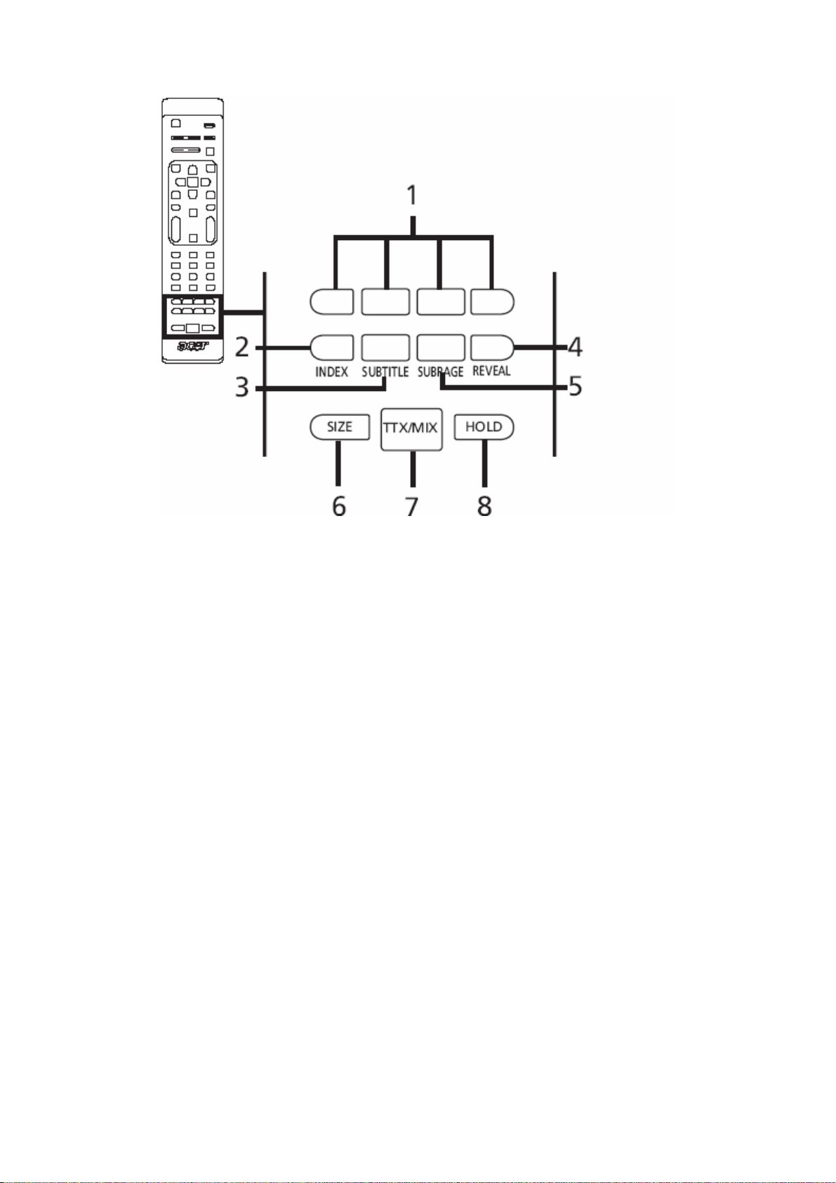
Teletext
1 Color buttons (R/G/Y/B)
Operates corresponding button on the teletext page.
2 INDEX
Press to go to the index page.
3 SUBTITLE
Press to view subtitles on the screen.
4 REVEAL
Press to reveal hidden teletext information.
5 SUBPAGE
Press to access the teletext’s subpages directly.
6 SIZE
Press once to zoom teletext page to 2X.
Press again to resume.
7 TTX/MIX (TELETEXT/MIX)
Press to switch from TV/AV to Teletext mode.
Press to overlay teletext page on the TV image.
8 HOLD
Press to pause the current teletext page in multi-page viewing mode.
16
Page 17
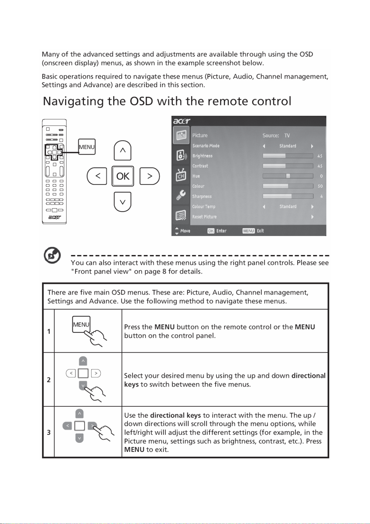
Using the OSD Menus
17
Page 18
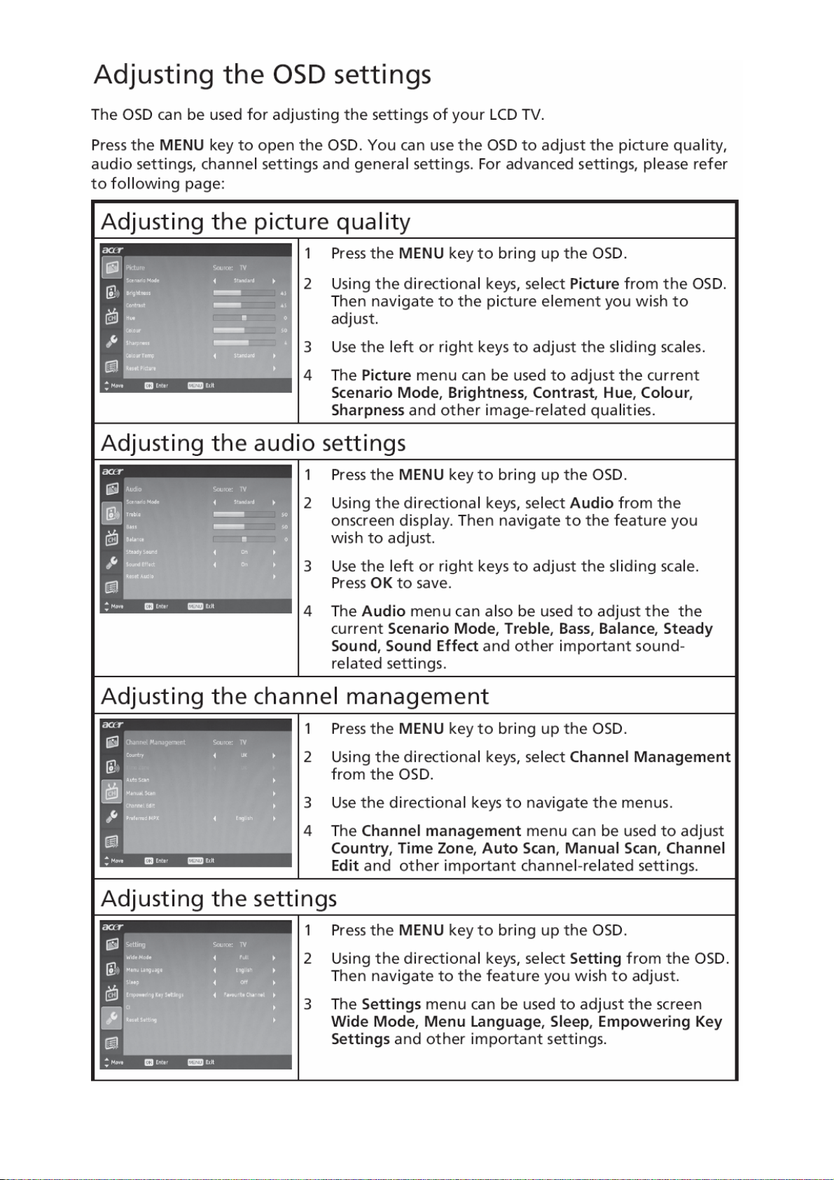
18
Page 19

19
Page 20
20
Page 21
21
Page 22

22
Page 23

23
Page 24

24
Page 25

Logo
When the monitor is power on, the LOGO will be showed in the center, and disappear slowly.
How To Optimize The DOS-Mode
Plug And Play
Plug & Play DDC2B Feature
This monitor is equipped with VESA DDC2B capabilities according to the VESA DDC STANDARD. It allows the
monitor to inform the host system of its identity and, depending on the level of DDC used, communicate additional
information about its display capabilities.
The DDC2B is a bi-directional data channel based on the I²C protocol. The host can request EDID information over
the DDC2B channel.
This monitor will appear to be non-functional if there is no video input signal. In order for this monitor to
operate properly, there must be a video input signal.
This monitor meets the Green monitor standards as set by the Video Electronics Standards Association (VESA)
and/or the United States Environmental Protection Agency (EPA) and The Swedish Confederation Employees
(NUTEK). This feature is designed to conserve electrical energy by reducing power consumption when there is no
video-input signal present. When there is no video input signals this monitor, following a time-out period, will
automatically switch to an OFF mode. This reduces the monitor's internal power supply consu mption. Af ter the video
input signal is restored, full power is restored and the display is automatically redrawn. The appearance is similar to
a "Screen Saver" feature except the display is completely off. The display is restored by p re ssing a key on the
keyboard, or clicking the mouse.
Using The Right Power Cord
The accessory power cord for the Northern American region is the wallet plug with NEMA 5-15 style and is UL listed
and CSA labe led. The voltage rating for the power cord shall be 125 volts AC.
Supplied with units intended for connection to power outlet of personal computer: Please use a cord set co nsisting of
a minimum No. 18 AWG, type SJT or SVT three conductors flexible cord. One end terminates with a grounding type
attachment plug, rated 10A, 250V, CEE-22 male configuration. The other end terminates with a molded-on type
connector body, rated 10A, 250V, having standard CEE-22 female configuration.
Please note that power supply cord needs to use VDE 0602, 0625, 0821 approval power cord in European cou nties.
25
Page 26

Machine Disassembly
Chapter 4
This chapter contains step-by-step procedures on how to disassemble the monitor for
maintenance.
The tools listed as below are that we may use during this procedure:
1. A proper screwdriver
2. A pair of glove
3. A pliers
4. A plastic knife
Disassembly Procedure
1. Remove the 3 screws to remove the stand.
2. Remove 9 screws to remove the rear cover.
26
Page 27

3. Remove 2 screws to remove the bkt-vesa.
4. Release the connectors.
27
Page 28

5. Remove the speakers.
6. Remove the main board, power board
28
Page 29

7. Remove the BKT-PCB-holder a nd BKT-panel-support.
8. Release the IR board.
9. Remove the bezel.
29
Page 30

10. Remove the 4 screws to release the panel.
30
Page 31

Trouble Shooting
Chapter 5
No picture (LED orange)
Check main board Standby power supply
Check key board/IR board
Check 24V power supply
No picture
OK
NG
Change key board/IR board
OK
NG
Check the power supply circuit
OK
NG
Change U902
OK
Check U401 Change U401
OK
Check I2C bus
NG
NG
Check I2C communication
31
Page 32

Abnormal display
Check the source
Check signal filter circuit
Check LVDS cable
Check panel
No sound
OK
OK
Check input
OK
OK
NG
NG
NG
Reset source
NG
Replace the filter or resistance
RF signal
Replace LVDS cable
Replace panel
OK
Check TV system setup
OK
Check Tuner
OK
Replace Tuner
Check the source
OK
Check if mute
OK
Check input signal
Check U401
OK
Check U601
OK
Check speaker
NG
OK
NG
NG
NG
Reset source
TV SIF
Check TU701
Change U401
Change U601
Change speaker
NG
Check TV
system
Change TU701
NG
Reset TV system
32
Page 33

No Power (No LED indicator)
Check power cord and board interface
OK
Check F901, BD901, C910
OK
Check D902, C920
OK
Check T901
NG
OK
Check D950, C952, C953, C954
No display (LED indicator green)
NG
NG
Replace T901
NG
NG
Plug in power cord and interface
Replace F901 or BD901 or C910
Replace D902 or C920
Replace D950 or C952 or C953 or C954
Check the source
OK
Check LVDS cable
NG
OK
Check 24V power supply
OK
Check BL ON/OFF signal
OK
Check C999 (+) 12V
NG
OK
Check IC903, IC970, IC971, IC904
OK
Check Q921, IC951, IC901
Reset source
Reset LVDS cable
NG
NG
Check B+ voltage, T902, D970, C975
Check U409
Replace C999
NG
NG
Replace IC903, IC970, IC971, IC904
Replace Q921, IC951, IC901
OK
Check U401
OK
Check panel
NG
NG
Replace U401
Replace panel
33
Page 34

Key Board
g
OSD is unstable or not workin
Is Key Pad Board connecting normally?
N
Connect Key Pad Board
Y
Is Button Switch normally?
Y
Is Key Pad Board Normally?
Y
Check Main Board
N
N
Replace Button Switch
Replace Key Pad Board
34
Page 35

Upgrade Firmware
Step 1: Install USB driver to your computer from the ISP board USB Driver file.
ISP board USB driver include three files:
Chapter 6
1. PL-2303 Driver InstallerV2021.exe
2. ser2pl.sys
3. UTS2pl.sys
4. Install PL-2303 Driver InstallerV2021.exe
Push "Next".
35
Page 36

Push "Finish".
5. ser2pl.sys & UTS2pl.sys two files should copy to C:\WINDOWS\system32\drivers & replace original files.
36
Page 37

Step 2: Connect to ISP Board.
Use USB port connecting PC & MT537x (or MT5335) Board via ISP board(Code number: 715G537XL2).
USB Cable
Use Desktop PC or Notebook USB Port
Step 3: Update TV.
I. Open the MtkTool to Load .bin file (Example: F3_dbg_image.bin) & Set Auto Set Flash BaudRate
37
Page 38

38
Page 39

II. Set COM port resource that used by USB Port.
III. Set Baud rate 115200 & High speed item Enable. & MT537x(MT5335).
39
Page 40

IV. Click "Upgrade" button.(Waiting for "Finished!" message.)
V. Main board Power Off _ On.
40
Page 41

White-Balance, Luminance Adjustment
Approximately 30 minutes should be allowed for warm up before proceeding white balance adjustment.
Chapter 7
YPbPr Mode display adjustment
White balance adjustment (B)
General set-up :
Equipment Requirements: Minolta CA-110 or Equivalent Color analyzer
Quantum Data Pattern Generator 802G , 802BT or equivalent instrument
Input requirements:
Input Signal Type: YPbPr signal
1. 720P mode, TVBar100 pattern by 802G or 8 02BT.
2. Select Smart picture to User mode and check the x, y data.
Input Signal Strength: 1 Vpp for Y signal; 700 mVpp for Pb & Pr signal
Input Injection Point: YPbPr (RAC jack)
720P, TVBar100 pattern
Alignment method:
Initial Set-up:
1. Select source as “Component”.
2. Set Smart picture as “User” and to be Contrast =50(TBD) (CMO), Brig htness=50(TBD) (CMO), at normal menu
mode.
3. Apply “TVBar100” pattern with color bar pattern by signal generator.
4. Enter factory mode menu: press “MENU+ “234” then enter FAC mode.
Alignment:
1. At FAC mode menu, select FACTORY->Picture ->ADC -> Auto Colour item. Then press “>” key to adjust
ADC_GAIN_R, ADC_GAIN_G, ADC_GAIN_B and ADC_OFFSET_R, ADC_OFFSET_G, ADC_OFFSET_B. Then
store those values to NVM.
White- Balance alignment :
1. Select source as “HDMI1”
2. Apply Flat pattern (100% white pattern) , at FAC mode menu, select Factory -> Picture -> Colour Temp item
3. Set color temperature to “Standard”.
4. Adjust the R Gain
those values to NVM.
5. Set color temperature to “Warm”.
6. Adjust the R Gain
those values to NVM.
7. Set color temperature to “Cold”.
8. Adjust the R Gain
those values to NVM.
, G_Gain, B_Gain values to meet “St andard” color coo rdinates spe cification below. Then store
, G_Gain, B_Gain values to meet “Warm” color coordinates specification below. Then store
, G_Gain, B_Gain values to meet “Cold” color coordinates specification below. Then store
41
Page 42

Color temperature Standard/Warm/Cold (x, y) co-ordinates specification:
Note:
1. Use Minolta CA-110 for color coordinates and luminance check.
2. Luminance > 400 cd/m
3. Reset AV setting, smart picture shall be recalled to be “Standard” and Contrast= (TBD) (CMO),
Brightness=(TBD) (CMO)
Picture Mode x Y
Normal (10000oK) 0.281±0.003 0.288±0.003
Warm (8000oK) 0.295±0.003 0.305±0.003
Cold (13000oK) 0.269±0.003 0.274±0.003
Table: Reading with Minolta CA-110.
2
in the center of the screen when Brightness control at 100; Contrast control at 100
PC mode display adjustment
WHITE-D adjustment (B)
General set-up:
Equipment Requirements: Minolta CA-110 or Equivalent Color analyzer
Chroma 2250 or equivalent PC signal generator
Input requirements:
Input Signal Type: PC VGA signal
1024X768/60Hz PC mode with PGCWRGB pattern. (see pattern-1)
Input Signal Strength: 0 .7 Vp-p linear voltage.
Input Injection Point: PC D-SUB input
Pattern-1
Alignment method:
Initial Set-up:
1. Select source as “VGA”.
2. Set Contrast = 50 (CMO) and Brightness=50 (CMO) , at Standard menu mode.
3. Apply “PGCWRGB”(pattern-1) pattern by VGA pattern generator.
4. Enter factory mode menu: press “MENU+ “234” then enter FAC mode
Alignment:
1. At FAC mode menu, select FACTORY->Picture ->ADC -> Auto Colour item. Then press “>” key to adjust
ADC_GAIN_R, ADC_GAIN_G, ADC_GAIN_B and ADC_OFFSET_R, ADC_OFFSET_G, ADC_OFFSET_B. Then
store those values to NVM.
42
Page 43

FRU (Field Replaceable Unit) List
This chapter gives you the FRU (Field Replaceable Unit) listing in global configurations of AT2645 & AT2646.Refer
to this chapter whenever ordering for parts to repair or for RMA (Return Merchandise Authorization).
NOTE: Please note WHEN ORDERING FRU PARTS, that you should check the most up-to-date information
available on your regional web or channel (http://aicsl.acer.com.tw/spl/). For whatever reasons a part number
change is made, it will not be noted in the printed Service Guide. For ACER AUTHORIZED SERVICE PROVIDERS,
your Acer office may have a DIFFERENT part number code from those given in the FRU list of this printed Service
Guide. You MUST use the local FRU list provided by your regional Acer office to order FRU parts for repair and
service of customer machines.
NOTE: To scrap or to return the defective parts, you should follow the local government ordinance or regulations on
how to dispose it properly, or follow the rules set by your regional Acer office on how to return it.
Chapter 8
43
Page 44

Exploded Diagram (Model: AT2645 & AT2646)
44
Page 45

EDID Data
DDC DATA for For D-SUB Input
EDID data (128 bytes)
**********************************************************************
45
Page 46

PCB Layout
Main Board Layout
Chapter 9
46
Page 47

Power Board
47
Page 48

Key Board
48
Page 49

Schematic Diagram
Main Board
NEARLY VGA CON.
GRN
GRN_GND
BLU R194
BLU_GND
RED
RED_GND
L111
1 2
80 OHM
C187
ZD121
5pF
1 2
C190
5pF
1 2
C194
5pF
UDZSNP5.6B
L112
80 OHM
ZD124
UDZSNP5.6B
L101
80 OHM
ZD126
UDZSNP5.6B
R191
1 2
R195
1 2
R200
1 2
Change to 75 OHM 1/8W
HDMIED_WP14,20
VGASCL_IN
VGASDA_IN
75 OHM +-1% 1/8W
75 OHM +-1% 1/8W
75 OHM +-1% 1/8W
C102
NC/5pF
R192
0 OHM 1/10W
C106
NC/5pF
R196
0 OHM 1/10W
C103
NC/5pF
R201
0 OHM 1/10W
R248
10K OHM 1/10W
R205 100 OHM 1/10W
R207 100 OHM 1/10W
ZD129
ZD128
1 2
1 2
UDZSNP5.6B
UDZSNP5.6B
CN109
PHONEJACK
CN108
DB15
HSYNC#
VSYNC#
1
VGAL_IN
2
VGAR_IN
3
1 2
C192
5pF
1 2
C196
5pF
ZD131
ZD130
1 2
1 2
VPORT0603100KV05
1
9
2
10
3
11
4
12
5
13
6
14
7
15
8
L113
80 OHM
ZD125
UDZSNP5.6B
L114
80 OHM
ZD127
UDZSNP5.6B
R218
1K OHM 1/10W
R219
1K OHM 1/10W
VPORT0603100KV05
RED
GRN
BLU
VGASDA_IN
HSYNC#
RED_GND
VSYNC#
GRN_GND
VGASCL_IN
BLU_GND
1 2
1 2
C181 470pF
R222
VGA_PLUGPWR
R198
2.2K OHM 1/10W
R203
2.2K OHM 1/10W
100K OHM 1/ 10W
C182 470pF
R244 NC
R245 NC
R220
3K OHM 1/10W
R221
3K OHM 1/10W
100K OHM 1/ 10W
R223
R224
C107
NC/5pF
C109
NC/5pF
30K OHM 1% 1/10W
U0RX 12
U0TX 12
HSYNC 4,13
VSYNC 4,13
R225
C135 33pF
30K OHM 1% 1/10W
C120
C122
10uF/10V
10uF/10V
C136 33pF
R204
20K OHM 1/10W
R206
20K OHM 1/10W
AIN0_L 10
AIN0_R 10
R188
0 OHM 1/10W
R189
39 OHM +-1% 1/10W
R193
100 OHM 1/10W
39 OHM +-1% 1/10W
R197
100 OHM 1/10W
R199
39 OHM +-1% 1/10W
R202
100 OHM 1/10W
VGA_PLUGPWR
Q102
MMBT3904
H : WP ENABLE
L : WP DISABLE
NEARLY IC
C101 4700pF
C186 0.01uF/25V
C188 0.01uF/25V
C189 0.01uF/25V
C191 0.01uF/25V
C193 0.01uF/25V
C195 0.01uF/25V
+5VSB
4.7KOHM +-5% 1/16W
1
2
3
4
2
1
RN101
SOG 4
GP 4
GN 4
BP 4
BN 4
RP 4
RN 4
D101
3
BAT54C
8
7
6
5
R165
NC
Chapter 10
C197
0.1UF16V
U105
VCC
E0
E1
WC
E2
SCL
VSSSDA
M24C02-WDW6P
1
2
3
45
8
7
6
T P V ( Top Victory Electronics Co . , Ltd. )
Date
T2848-H-X-X-2-032408
VGA IN/L/R
絬 隔 瓜 絪 腹
Key Component
49
OEM MODEL Size
AT2645 B
TPV MODEL
TV2668W-AED C
PCB NAME
715T2848-H
Sheet
322Friday, April 11, 2008
of
Rev
称爹
<
称爹
>
Page 50

CN105
JACK
CN106
JACK
NEARLY YPBPR CONNECTOR
PR0_IN
2
PB_GND
1
PB0_IN
4
PB_GND
3
Y0_IN
6
Y_GND
5
2
1
4
3
Y0_IN
Y_GND
PB0_IN
PB_GND
PR0_IN
R175
1K OHM 1/10W
R176
1K OHM 1/10W
ZD120
ZD119
1 2
1 2
VPORT0603100KV05
VPORT0603100KV05
L108
1 2
80 OHM
C171
100pF
L109
1 2
80 OHM
C172
100pF
C173
100pF
L110
1 2
80 OHM
C198 470pF
ZD116
UDZSNP5.6B
ZD117
UDZSNP5.6B
ZD118
UDZSNP5.6B
Change to 75 OHM 1/8W
YPBPR0L_IN
YPBPR0R_IN
R177
100K OHM 1/ 10W
R129
3K OHM 1/10W
R130
3K OHM 1/10W
R178
C199 470pF
100K OHM 1/ 10W
Y0_IN_OUT
R209
75 OHM +-1% 1/8W
PB0_IN_OUT
R210
75 OHM +-1% 1/8W
R211
75 OHM +-1% 1/8W
PR0_IN_OUT
R105
0 OHM 1/10W
R106
68 OHM 1/10W
R107
100 OHM 1/10W
R108
68 OHM 1/10W
R110
100 OHM 1/10W
R111
68 OHM 1/10W
NEARLY MT5335
R243
C208 33pF
30K OHM 1/ 10W
C131 10uF/10V
C132 10uF/10V
R242
C209 33pF
30K OHM 1/ 10W
C104 4700pF
C105 0.01uF/25V
C108 0.01uF/25V
C111 0.01uF/25V
C114
C116 0.01uF/25V
R246
20K OHM 1/10W
R247
20K OHM 1/10W
SOY1
Y1P
Y1N
PB1P
PBR1N
PR1P
AIN1_L 10
AIN1_R 10
SOY06
Y0P6
Y0N6
PB0P6
PBR0N6
PR0P6
SOY1
Y1P
Y1N
PB1P
PBR1N
PR1P
SOY0
Y0P
Y0N
PB0P
PBR0N
PR0P
TP101
TP106
AV12
AV12
AV12
107
108
109
114
115
116
118
119
120
121
122
123
112
111
FB101
BEAD
FB107
BEAD
FB108
BEAD
U401E
SOY0
Y0P
Y0N
PB0P
PBR0N
PR0P
SOY1
Y1P
Y1N
PB1P
PBR1N
PR1P
TN1
TP1
MT5335PKU
DVDD12_VGA
AVSS12_RGBADC
AVDD12_RGBADC
AVSS12_RGBFE
AVDD12_RGBFE
VSYNC
HSYNC
SOG
DVDD12_VGA
C174
1uF/16V
AVDD12_RGBADC
C176
10uF/10V
AVSS12_RGBADC
AVDD12_RGBFE
C179
1uF/16V
AVSS12_RGBFE
RP
RN
BP
BN
GP
GN
117
113
110
105
101
104
106
98
99
102
103
96
97
100
C175
0.1UF16V
C177
0.1UF16V
C180
0.1UF16V
DVDD12_VGA
AVSS12_RGBADC
AVDD12_RGBADC
AVSS12_RGBFE
AVDD12_RGBFE
RP 3
RN 3
BP 3
BN 3
GP 3
GN 3
VSYNC 3,13
HSYNC 3,13
SOG 3
ASPDIF10
R183
100 OHM 1/10W
C119
100pF
R184
1 2
30 OHM
R185
100 OHM 1/10W
R186
NC
C183
0.1UF16V
C185
100pF
SPDIF_OUT
12
ZD101
VPORT0603100KV05
---><---|>
CN107
2
1
JACK
OEM MODEL Size
TPV MODEL
PCB NAME
AT2645 B
TV2668W-AED C
715T2848-H
Sheet
of
422Friday , April 11, 2008
Rev
称爹
<
称爹
>
50
T P V ( Top Victory Electronics Co . , Ltd. )
絬 隔 瓜 絪 腹
Key Component
T2848-H-X-X-2-032408
YPbPR/L/R & SPDIF
Date
Page 51

SC1_IN
CN103
4
2
6
DIN JACK
CN104
7
9
8
4
6
5
1
3
JACK
2
Near Connector
AV1R_IN
AV1L_IN R170
R226 1K OHM 1/10W
R227 1K OHM 1/10W
ZD114
ZD113
1 2
1 2
VPORT0603100KV05
VPORT0603100KV05
SY1_IN
3
1
5
AV1_IN
AV1L_IN
AV1R_IN
R232
3K OHM 1/10W
C200 470pF
R228
R229
C201 470pF
100K OHM 1/ 10W
100K OHM 1/ 10W
SY1_IN
SC1_IN
R233
3K OHM 1/10W
C202 33pF
30K OHM 1/10W
R230
NEARLY AV CONNECTOR
R162 27 OHM 1/10W
R164
ZD111
UDZSNP5.6B
R166 27 OHM 1/10W R167
ZD112
UDZSNP5.6B
C157 2.2uF/16V
C160 2.2uF/16V
C203 33pF
R231
30K OHM 1/10W
47 OHM 1/10W
R168
47 OHM 1/10W
R169
20K OHM 1/10W
20K OHM 1/10W
C152
47pF
C156
47pF
NEARLY MT5380
R163
100 OHM 1/10W
100 OHM 1/10W
AIN2_R 10
AIN2_L 10
CVBS018
C151 0.047uF
C154 0.047uF
Close to MT5382p
R179
100 OHM 1/10W
R182
NC
SY1
SC1
C117
0.047uF
U401F
132
CVBS0
CVBS1
SY06
SC06
SY1
SC1
D2SA
TP105
AV25
AV25
AV25
130
129
128
127
126
125
136
FB103
BEAD
FB104
BEAD
C161
4.7uF/10V
FB105
BEAD
CVBS1
CVBS2
SY0
SC0
SY1
SC1
D2SA
MT5335PKU
DVDD25_VADC
DVSS25_VADC
GND_TUNER
GD_CVBS
GND_SV
AVDD25_VADC
AVSS25_VADC
AVDD25_REF
AVSS25_REF
AVDD25_VFE
AVSS25_VFE
DVDD25_VADC
C158
1uF/16V
DVSS25_VADC
AVDD25_VADC
C162
1uF/16V
AVSS25_VADC
AVDD25_REF
C165
1uF/16V
AVSS25_REF
139
140
133
131
124
141
142
137
138
135
134
C159
0.1UF16V
C163
0.1UF16V
C166
0.1UF16V
DVDD25_VADC
DVSS25_VADC
GND_CVBS
GND_SV
AVDD25_VADC
AVSS25_VADC
AVDD25_REF
AVSS25_REF
AVDD25_VFE
AVSS25_VFE
GND_TUNER 18
C118
1uF/16V
GND_SV 6
AV25
AV1_IN
R171
27 OHM 1/10W
UDZSNP5.6B
ZD115
R173
47 OHM 1/10W
C167
47pF
R174
0 OHM 1/10W
R172
100 OHM 1/10W
C164 0.047uF
C168 1uF/16V
51
CVBS1
GND_CVBS
T P V ( Top Victory Electronics Co . , Ltd. )
Date
T2848-H-X-X-2-032408
S-video/CVBS/L/R
絬 隔 瓜 絪 腹
Key Component
FB106
BEAD
OEM MO D E L Si ze
TPV MODEL
PCB NAME
AVDD25_VFE
C169
1uF/16V
AVSS25_VFE
AT2645 B
TV2668W-AED C
715T2848-H
of
522Friday , April 11, 2008
Sheet
C170
0.1UF16V
Rev
称爹
<
称爹
>
Page 52

NEARLY IC
R143
100 OHM 1/10W
R146
68 OHM 1/10W
R149
100 OHM 1/10W
R150
68 OHM 1/10W
R153
100 OHM 1/10W
R156
68 OHM 1/10W
R215
100 OHM 1/10W
3K OHM 1/10W
R241
30K OHM 1/ 10W
C138 0.047uF
C140 1uF/16V
C141 0.01uF/25V
C143 0.01uF/25V
C144 0.01uF/25V
C146 0.01uF/25V
C148 0.01uF/25V
C134 0.047uF
R237
C205 33pF
R240
30K OHM 1/ 10W
C204 33pF
SY0 5
GND_SV 5
Y0P 4
Y0N 4
PB0P 4
PBR0N 4
PR0P 4
SC0 5
C149 2.2uF/16V
C150 2.2uF/16V
C113
560pF
C115
560pF
SCT1_AUR_IN
SCT1_AUL_IN
SCT1_FS_IN
SCT1_FB_IN
SCT1_AV_IN
CN102
2
4
6
8
10
12
14
16
18
20
SCART
Full SCART
SCT1_FB_IN
ZD109
UDZSNP5.6B
SCT1_FS_IN
ZD110
RLZ13B
R158
33K OHM 1/10W
1 2
1
3
5
7
9
11
13
15
17
19
21
R155
0 OHM 1/10W
R157
75 OHM 1/10W
1000pF/25V
SCT1_AUR_OUT
SCT1_AUL_OUT
SCT1_B_IN
SCT1_G_IN
SCT1_R_IN
SCT1_AVO_GND
SCT1_AV_OUT
SOY0 4
SCART_FS_IN 9
R161
10K OHM 1/10W
C112
C110
1000pF/25V
SCT1_AUR_OUT 16
SCT1_AUL_OUT 16
SCT1_AVO_GND 18
SCT1_AV_OUT 18
NEARLY CONNECTOR
SCT1_AV_IN
SCT1_G_IN
SCT1_B_IN
SCT1_R_IN
SCT1_AUR_IN
SCT1_AUL_IN
R142 27 OHM 1/10W
ZD105
UDZSNP5.6B
L105
1 2
80 OHM
ZD106
UDZSNP5.6B
L106
1 2
80 OHM
ZD107
UDZSNP5.6B
ZD108
L107
UDZSNP5.6B
1 2
80 OHM
Change to 75 OHM 1/8W
ZD132
1 2
R144
47 OHM 1/ 10W
R147
75 OHM 1/ 8W
R151
75 OHM 1/ 8W
R154
75 OHM 1/ 8W
R238 1K OHM 1/10W
R239 1K OHM 1/10W
ZD133
VPORT0603100KV05
1 2
VPORT0603100KV05
C207
EMI
C139
47pF
C142
15pF/50V
C145
15pF/50V
C147
15pF/50V
NC/470pF
R234
R145
0 OHM 1/10W
R148
0 OHM 1/10W
R152
0 OHM 1/10W
C206
100K OHM 1/ 10W
EMI
R236
3K OHM 1/10W
NC/470pF
R235
100K OHM 1/ 10W
NEARLY MT5335
R159
20K OHM 1/10W
R160
20K OHM 1/10W
Audio In 1V
AIN3_R 10
AIN3_L 10
52
T P V ( Top Victory Electronics Co . , Ltd. )
絬 隔 瓜 絪 腹
Key Component
T2848-H-X-X-2-032408
SCART connec t or
Date
OEM MO D E L Size
TPV MO D E L
PCB NAME
AT2645 B
TV2668W-AED C
715T2848-H
Sheet
of
622Friday , April 11, 2008
Rev
称爹
称爹
>
<
Page 53

For 26" Panel
LVDS 12V
DV33
L301
NC
L302
12V
1 2
BEAD
+5V
L303
NC/BEAD
LVDSVDD_EN9
HI = > L V DS POW ER ON
LO = > LVDS POWER OFF
A0N
A0P
A1N
A1P
A2N
A2P
CK1N
CK1P
A3N
A3P
A4N
A4P
A5N
A5P
A6N
A6P
CK2N
CK2P
A7N
A7P
3A
R306
51K OHM 1/10W
U401C
244
243
242
241
240
239
237
236
235
234
233
232
231
230
228
227
226
225
224
223
222
221
A0N
A0P
A2N
A2P
CK1N
CK1P
A3N
A3P
A4N
A4P
A5N
A5P
A6N
A6P
A7N
A7P
CK2N
CK2P
A8N
A8P
A9N
A9P
MT5335PKU
AVDD33_LVDSA
AVDD33_LVDSB
AVDD33_LVDSC
AVDD33_VPLL
LVDS OUT
+
C310
220uF/16V
T1= 0.74ms>0.47ms
R307
1M OHM 1/10W
C311
0.1UF16V
C301
1uF6.3V
TP2
TN2
C312
NC/1uF/16V
R305
10K OHM 1/10W
Q301
2N7002 SOT-23
220
229
238
217
218
219
R302
100K OHM 1/1 0W
AVDD33_LVDS
AVDD33_LVDS
AVDD33_LVDS
AVDD33_VPLL
CI_POCE1# 20
U301
1
S
2
3
4
AO4449 -7A/-30V
D
S
D
S
D
G
D
8
7
6
5
+
C308
NC/100uF/16V
LVDSVDD
C309
0.1UF16V
AV33
C303
1uF/16V
AV33
1 2
+
C305
100uF/16V
FB301
BEAD
FB302
BEAD
CK1P
22 OHM 1/10W
CK2P
22 OHM 1/10W
DV33
AVDD33_LVDS
C302
10uF/10V
1206
AVDD33_VPLL
C306
1uF/16V
NC FOR FFC Board
LVDSVDD
A0N
A1N
A2N
R308
R310
A3P
A4P
A5N
A6P
A7P
FB303
BEAD
SELLVDS 3.3V
C304
0.1UF16V
C307
0.1UF16V
33T8027 30 GP
CN301
12
34
56
78
910
11 12
13 14
15 16
17 18
19 20
21 22
23 24
25 26
27 28
29 30
NC/CONN
LVDSVDD
A0P
A1P
A2P
A3N
A4N
A5P
A6N
A7N
CK1N
R309
22 OHM 1/10W
CK2N
R311
22 OHM 1/10W
T P V ( Top Victory Electronics Co . , Ltd. )
絬 隔 瓜 絪 腹
Key Component
Date
T2848-H-X-X-2-032408
LVDS OU T
53
OEM MO D E L Si ze
TPV MO DE L
PCB N AME
Sheet
AT2645 A4
TV2668W-AED C
715T2848-H
722Friday, April 11, 2008
of
Rev
称爹
<
称爹
>
Page 54

AV12
FB411
BEAD
C502
AV33
1uF/16V
FB401
BEAD
U401D
TP409
TP410
157
158
68
65
66
67
69
USB_VRT
USB_DM
USB_DP
AVDD33_USB
AVDD12_USB
TP0
TN0
MT5335PKU
AVDD12_ADCPLL
AVDD12_TVDPLL
AVDD12_HDMIPLL
AVDD12_SYSPLL
AVDD12_DTDPLL
AVDD12_APLL
AVDD12_DMPLL
USB_VRT
USB_D-12
USB_D+12
USB_DUSB_D+
AVDD33_USB
AVDD12_USB
160
155
153
161
159
156
154
AVDD12_PLL
AVDD12_PLL
AVDD12_PLL
AVDD12_PLL
AVDD12_PLL
AVDD12_PLL
AVDD12_PLL
AVDD12_PLL
C503
4.7uF/10V
AVDD33_USB
C506
4.7uF/10V
C504
0.01uF/25V
C507
0.1UF16V
C505
0.1UF16V
TS_VALIDO20
TS_C KO20
USB_VRT
MPX0P18
MPX0N18
RX0_CB15
RX0_C15
RX0_0B15
RX0_015
RX0_1B15
RX0_115
RX0_2B15
RX0_215
R470 5.1K OHM 1/10W
U401H
164
SIFP
166
167
194
79
80
81
82
83
84
85
86
SIFN
AF
TUNER_CLK
MT5335PKU
U401K
RX0_CB
RX0_C
RX0_0B
RX0_0
RX0_1B
RX0_1
RX0_2B
RX0_2
MT5335PKU
RX0_CB
RX0_C
RX0_0B
RX0_0
RX0_1B
RX0_1
RX0_2B
RX0_2
TP411
AVDD25_SADC
AVSS25_SADC
RF_AGC
IF_AGCTUNER_DATA
EXT_RES
OPWR0_5V
AVDD33_HDMI
AVDD12_CVCC
AVDD25_SADC
163
165
AVSS25_SADC
193
192195
77
73
AVDD33_H
78
AVDD12_CVCC
74
TP401
TS_DATAO 20
TS_SYNCO 20
HDMI_5V
AV12
AV25
AV33
AV12
FB412
BEAD
C508
10uF/10V
FB413
BEAD
C511
1uF/16V
FB414
BEAD
C517
1uF/16V
FB415
BEAD
C518
1uF/16V
AVDD12_USB
C509
4.7uF/10V
AVDD25_SADC
C512
4.7uF/10V
AVSS25_SADC
AVDD33_H
C515
4.7uF/10V
AVDD12_CVCC
C519
4.7uF/10V
C510
0.1UF16V
C513
0.01uF/25V
C516
0.1UF16V
C520
0.1UF16V
C514
0.1UF16V
T P V ( Top Victory Electronics Co . , Ltd. )
絬 隔 瓜 絪 腹
Key Component
Date
T2848-H-X-X -2-032408
MT5335 HDMI/ P LL
54
OEM MO DE L S i ze
TPV MO DE L
PCB NAME
Sheet
AT2645 A4
TV2668W-AED C
715T2848-H
822Friday , April 11, 2008
of
Rev
称爹
<
称爹
>
Page 55

BL_DIM21
+3V3SB
+3V3SB
+3V3SB
R446
+
C488
TUR N_ON
STANDBY
KEY113
3.9K OH M 1/1 0W
NC/220uF/ 10V
R449
NC/220 OH M 1/10W
R450
NC/ 47K OH M 1/10W
C452
NC/1000pF/25V
KEY1
KEY2
R458
+3V3SB_uP
4.7K OHM 1/10W
4.7K OHM 1/10W
R493
R492
OPWM120
KEY2
EDID_PRT
FB408
BEAD
FB410
BEAD
MTK_IC_RESET20
R488 33 OHM 1/10W
SCART_FS_IN6
POWER_ON/OFF21
10K OHM 1/10W
HDMI_INT13
AVCC_SRV
C494
1uF/16V
AVDD33_XTAL
C500
1uF/16V
OSDA0
OSDA013,19
OSCL0
OSCL013,19
OSDA115
OSCL115
OPWM212, 20
OXTALO
OXTALI
AVCC_SRV
AVDD33_XTAL
KEY1_MT5335
PWRDET
AVDD33_REG
C_XREG
ORESET#
+3V3SB
+3V3SB
Q403
C501
0.1UF16V
R445
10K OHM 1/10W
+3V3SB
R444
MMBT3904
R420 NC
R461 10K OHM 1/10W
R463
10K OHM 1/10W
C495
0.1UF16V
204
205
63
62
191
202
203
146
143
144
147
145
152
151
150
149
148
88
87
72
R456
10K OHM 1/10W
FB409
BEAD
U401B
OSDA0
OSCL0
OSDA1
OSCL1
OPWM0
OPWM1
OPWM2
VCXO
XTALO
XTALI
AVDD33_SR V
AVDD33_XTAL
ADIN4
ADIN3
ADIN2
ADIN1
ADIN0
AVDD33_R EG
C_XREG
OPWRSB
MT5335PKU
DV33
Q406
MMBT3904
AVDD33_REG
C498
1uF/16V
R459
33 OHM 1/10W
OSCL0
OSDA0
R464
C499
0.1UF16V
GPIO_3
GPIO_4
GPIO_5
GPIO_6
GPIO_7
GPIO_8
GPIO_9
GPIO_10
GPIO_11
GPIO_12
GPIO_13
OPCTRL0
OPCTRL1
OPCTRL2
OPCTRL3
OPCTRL4
OPCTRL5ORESET_
NC/ 10K OH M 1/10W
CEC13,14
8
7
6
4.7K OHM 1/10W
4.7K OHM 1/10W
R465
DV33
207
208
209
59
60
210
211
212
214
215
216
92
91
76
75
90
8971
R426
4.7K OHM 1/ 10W
+3V3SB
R486
NC/MMBT3904
U405
1
NC
VCC
2
NC
WC
3
NC
SCL
45
VSSSDA
M24C 16
IIC ADDRESS "A0"
KEY1_MT5335
+3V3SB
Q408
R495
NC
DV33
CI_PDD3 20
CI_PDD4 20
CI_PDD5 20
CI_PDD6 20
CI_PDD7 20
CI_POWE# 20
CI_OEB 20
CI_ALE 20
CI_CLE 20
LVDSVDD_EN 7
CI_INT 20
AMP_MUTE 17
BL_ON/OFF 21
EDID_PRT
+3V3SB
R487
NC/10K OH M 1/10W
C492
1uF/16V
SCS140V
D403
KEY1
12
DV33
R448
1K OHM 1/10W
PWRDET
D401
NC/LL4148
Adjust the power on timing
R454
C_XREG
1 OHM +-5% 1/10W
C491
4.7uF/ 10V
The divider only for A version IC
TURN_ON13
uP default High
High ON Low OFF
STANDBY13
uP default High
High ON Low OFF
For OTS pull high
R447
NC/ 1K OH M 1/ 10W
ORESET#
Q404
NC/MMBT3904
+5VSB
+3V3SB
R497
NC
3.344V
ORESET#
Low Reset (Low--> High 3.3V)
56T 643 35 MAX809STRG(140ms)
56T 643 5B G690H293T73UF(140ms)
For OTS
+5V
47K OHM 1/10W
R427
3K OHM 1/10W
C441
NC/1000pF/25V
+3V3SB_uP
C493
4.7uF/ 10V
+3V3SB_uP
R489
3.9K OH M 1/1 0W
C497
C496
1000pF
1000pF
3
U408
2
RESET
MAX809STRG
1
R462
R453
NC/0 OH M 1/10W
R455
NC/0 OHM 1/10W
R452
+5VSB
+3V3SB_uP
Keypad
power
R466 0 OHM 1/10W
R467 0 OHM 1/10W
NC/ 470K OH M 1/10W
R498
820 OHM 1% 1/10W
R499
1.8K OHM 1% 1/ 10W
VCC
FOR SPARK TEST
GND
+3V3SB_uP
R460
1K OHM 1/10W
Q405
MMBT3906
0 OHM 1/10W
+3V3SB_uP
R468
OXTALI
NC
Y401
TXC
12
60MHz
C489
10pF
Third-Tone Crystal
+5V
R428
1K OHM 1/10W
Pull high
潮伐
LED
CN404
1
2
3
OIRI12,13
4
5
6
7
8
9
10
11
CONN
ZD410
UDZSNP5.6B
R469
NC/ 470K OH M 1/10W
1 2
OXTA LO
C490
10pF
Lock Type
ZD411
UDZSNP5.6B
1 2
L401
0.82UH
C401
1000pF
T P V ( Top Victory Electronics Co . , Ltd. )
T2848-H-X-X-2-032408
絬 隔 瓜 絪 腹
Key Component
MT5335 Control/IR/LED/Key
Date
55
OEM MO D EL Size
AT2645 A3
TPV MODEL
TV2668W-AED C
PCB NAME
715T2848-H
Sheet
of
922Friday , A pril 11, 2008
Rev
称爹
>
称爹
<
Page 56

U401G
AIN0_L3
AIN0_R3
AIN1_L4
AIN1_R4
AIN2_L5
AIN2_R5
AIN3_L6
AIN3_R6
AVDD33_AADC
AVSS33_AADC
VIMD_AADC
REFP_AADC
REFN_AADC
177
176
175
174
173
172
171
170
169
181
179
180
178
MT5335PKU
AIN0_L
AIN0_R
AIN1_L
AIN1_R
AIN2_L
AIN2_R
AIN3_L
AIN3_R
AVDD33_AADC
AVSS33_AADC
VMID_AADC
REFP_AADC
REFN_AADC
ASPDIF
AOMCLK
AOLRCK
AOSDATA0
ADAC_VCM
AVDD33_DIG
AOBCK
AL1
AR1
AL2
AR2
AVDD33_ADAC0
AVDD33_ADAC1
AVSS33_ADAC0
AVSS33_ADAC1
201
AOMCLK
198
AOLRCK
199
AOBCK
200
MT5133_RESET
196
186
185
189
187
AVDD33_ADAC0
190
AVDD33_ADAC1
182
AVSS33_ADAC0
188
AVSS33_ADAC1
184
ADAC_VCM
183
AVDD33_DIG
168
ASPDIF 4
TP402
AOLRCK 12
AOBCK 12
MT5133_RESET 19
AL1O 16
AR1O 16
AL2O 16
AR2O 16
ADAC_VCM
+
C472
10uF/16V
C473
0.1UF16V
AV33
FB403
BEAD
+
C474
100uF/16V
FB406
AV33
BEAD
AV33
FB407
BEAD
T P V ( Top Victory Electronics Co . , Ltd. )
絬 隔 瓜 絪 腹
Key Component
T2848-H-X-X - 2-032408
MT5335 Audio In/Out
Date
AVDD33_AADC
C475
1uF/16V
AVSS33_AADC
REFP_AADC
C482
1uF/16V
REFN_AADC
AVDD33_ADAC0
C484
1uF/16V
AVSS33_ADAC0
AV33
FB404
BEAD
C476
0.1UF16V
AV33
FB405
BEAD
C483
0.1UF16V
C485
0.1UF16V
OE M MOD EL Size
TPV MO DE L
PCB N AME
Sheet
C479
4.7uF/10V
AT2645 A4
TV2668W-AED C
715T2848-H
of
10 22Friday , April 11, 2008
AVDD33_ADAC1
C477
1uF/16V
AVSS33_ADAC1
AVDD33_DIG
C480
1uF/16V
AVSS33_DIG
VIMD_AADC
C486
4.7uF/10V
C487
0.1UF16V
C478
0.1UF16V
C481
0.1UF16V
Rev
称爹
称爹
>
<
56
Page 57

RDQS0
RDQM0
RDQ0
RDQ1
RDQ2
RDQ3
RDQ4
RDQ5
RDQ6
RDQ7
RDQS1
RDQM1
RDQ8
RDQ9
RDQ10
RDQ11
RDQ12
RDQ13
RDQ14
RDQ15
MEM_VRE F
RCS#
MEM_AD DR12
MEM_AD DR11
MEM_AD DR9
MEM_AD DR8
MEM_AD DR7
MEM_AD DR6
MEM_AD DR5
MEM_AD DR4
MEM_WE#
MEM_CAS#
MEM_RAS#
MEM_CS#
MEM_BA0
MEM_BA1
MEM_AD DR10
MEM_AD DR0
MEM_AD DR1
MEM_AD DR2
MEM_AD DR3
DDRV
+
U401A
11
RDQS0
13
RDQM0
9
RDQ0
8
RDQ1
7
RDQ2
6
RDQ3
5
RDQ4
4
RDQ5
3
RDQ6
2
RDQ7
17
RDQS1
15
RDQM1
19
RDQ8
20
RDQ9
21
RDQ10
22
RDQ11
23
RDQ12
24
RDQ13
25
RDQ14
26
RDQ15
53
RVREF0
46
RCS_
MT5335PKU
RN406 47 OHM 1/16W
5
6
7
8
RN408 47 OHM 1/16W
5
6
7
8
RN409 47 OHM 1/16W
5
6
7
8
RN410 47 OHM 1/16W
5
6
7
8
RN415 47 OHM 1/16W
5
6
7
8
RWE_
RBA0
RBA1
RRAS_
RA10
RCAS_
RA12
RCKE
RA11
RCLK0_
RCLK0
4
3
2
1
4
3
2
1
4
3
2
1
4
3
2
1
4
3
2
1
Add serial resistors for DRAM
C440
4.7uF/10V
C435
0.1UF 16V
C433
100uF/16V
RA0
RA7
RA6
RA5
RA8
RA4
RA9
RA3
RA1
RA2
For EMI
U402A
47
RA0
36
RA7
40
RWE#
43
RBA0
37
RA6
44
RBA1
38
RA5
42
RRAS#
35
RA8
45
RA10
39
RA4
41
RCAS#
32
RA12
31
RCKE
33
RA11
34
RA9
51
RA3
49
RA1
50
RA2
28
RCLK0#
29
RCLK0
RA12
RA11
RA9
RA8
RA7
RA6
RA5
RA4
RWE#
RCAS#
RRAS#
RCS#
RBA0
RBA1
RA10
RA0 MEM_DQ11
RA1
RA2
RA3
FB416
BEAD
C448
0.01uF/25V
C450
0.01uF/25V
FB417
BEAD
C434
0.1UF16V
C436
0.1UF16V
C437
0.1UF16V
C439
0.1UF16V
MEM_ADD R 12
MEM_ADD R 11
MEM_ADD R 10
MEM_ADD R 9
MEM_ADD R 8
MEM_ADD R 7
MEM_ADD R 6
MEM_ADD R 5
MEM_ADD R 4
MEM_ADD R 3
MEM_ADD R 2
MEM_ADD R 1
MEM_ADD R 0
MEM_BA1
MEM_BA0
MEM_R AS #
MEM_C AS #
MEM_W E#
MEM_D QM1
MEM_D QM0
MEM_C LK0#
MEM_C LK0
MEM_C LKEN
C438
0.1UF16V
DDRV_BEAD2
C451
0.01uF/25V
DDR SDRAM
42
RES(A12)
41 2
A11 DQ0
28
A10
40
A9
39
A8
38
A7
37
A6
36
A5
35
A4
32
A3
31
A2
30
A1
29
A0
27
BA1
26
BA0
23
RAS
22
CAS
21
WE
47
UDM
20 51
LDM UDQS
46
CK
45
CK
HY5DU121622DTP-D43
RCKE
R432
22 OHM 1/10W
R433
RCLK0
22 OHM 1/10W
R439
RCLK0#
22 OHM 1/10W
DDRV_BEAD1
C951
0.1UF16V
DQ1
DQ2
DQ3
DQ4
DQ5
DQ6
DQ7
DQ8
DQ9
DQ10
DQ11
DQ12
DQ13
DQ14
DQ15
LDQS
CSCKE
C449
0.01uF/25V
4
5
7
8
10
11
13
54
56
57
59
60
62
63
65
16
2444
DDR#1
MEM_DQ0
MEM_DQ1
MEM_DQ2
MEM_DQ3
MEM_DQ4
MEM_DQ5
MEM_DQ6
MEM_DQ7
MEM_D Q8
MEM_DQ9
MEM_DQ10
MEM_D Q1 1
MEM_D Q1 2
MEM_DQ13
MEM_DQ15
MEM_DQ14
MEM_DQS1
MEM_DQS0
MEM_CS#
MEM_CLKEN
MEM_CLK0
MEM_CLK0#
MEM_VR EF
VTT
R434
100 OHM 1/10W
C443
0.1UF 16V
C465
0.1UF 16V
MEM_ADD R 13
MEM_VR EF
Swap for layout
MEM_VRE F
C444
0.1UF16V
+1V3D
C466
0.1UF16V
C445
4.7uF/10V
C467
0.1UF16V
U402B
DDR SDRAM
(PWR)
14
NC1
17
NC2
19
NC3
25
NC4
43
NC5
50
NC6
53
NC7
49
VREF
HY5D U121622DTP-D43
+1V3D
C471
4.7uF/10V
1
VDD1
18
VDD2
33
VDD3
3
VDDQ1
9
VDDQ2
15
VDDQ3
55
VDDQ4
61
VDDQ5
34
VSS1
48
VSS2
66
VSS3
6
VSSQ1
12
VSSQ2
52
VSSQ3
58
VSSQ4
64
VSSQ5
RDQ0
RN411 47 OHM 1/16W
RDQ1
RDQ2
RDQ3
RN413 47 OHM 1/16W
RDQ4
RDQ5
RDQ6
RDQ7
RDQS0
R435 47 OHM 1/16W
R437 47 OHM 1/16W
RDQM0
RDQM1
R440 47 OHM 1/16W
R442 47 OHM 1/16W
RDQS1
RDQ8
RN416 47 OHM 1/16W1
RDQ9
RDQ10
RDQ11
RDQ12
RN418 47 OHM 1/16W1
RDQ13
RDQ14
RDQ15
C457
C458
0.1UF16V
0.1UF16V
DDRV_BEAD1
DDRV
DDRV_BEAD1
DDRV_BEAD2
5
6
7
8
5
6
7
8
8
7
6
5
8
7
6
5
C459
0.1UF 16V
75 OHM/NC
75 OHM/NC
4
3
2
1
4
3
2
1
2
3
4
2
MEM_D Q1 4
3
MEM_D Q1 5
4
MEM_W E#
MEM_C AS #
MEM_R AS #
MEM_C S#
MEM_BA0
MEM_BA1
MEM_ADD R 10
+1V3D
MEM_ADD R 4
MEM_ADD R 5
MEM_ADD R 6
MEM_ADD R 7
MEM_C LKEN
MEM_ADD R 12
MEM_ADD R 11
MEM_ADD R 9
MEM_ADD R 8
MEM_ADD R 0
MEM_ADD R 1
MEM_ADD R 2
MEM_ADD R 3
MEM_ADD R 13
MEM_DQ0
MEM_DQ1
MEM_DQ2
MEM_DQ3
MEM_DQ4
MEM_DQ5
MEM_DQ6
MEM_DQ7
MEM_DQS0
MEM_DQM0
MEM_DQM1
MEM_DQS1
MEM_DQ8
MEM_DQ9
MEM_DQ10
MEM_DQ12
MEM_DQ13
MEM_DQ15
MEM_DQ14
Swap for layout
C461
C460
0.1UF 16V
0.1UF16V
RN402 8P4R 75 OH M +-5% 1/16W1
8
2
7
3
6
4
5
RN403 8P4R 75 OH M +-5% 1/16W1
8
2
7
3
6
4
5
RN404 8P4R 75 OH M +-5% 1/16W1
8
2
7
3
6
4
5
R430 NC
RN405 8P4R 75 OH M +-5% 1/16W
RN407 8P4R 75 OH M +-5% 1/16W1
R431 NC
RN412 8P4R 75 OH M +-5% 1/16W1
RN414 8P4R 75 OH M +-5% 1/16W1
RN417 8P4R 75 OH M +-5% 1/16W1
RN419 8P4R 75 OH M +-5% 1/16W1
C462
0.1UF16V
4
5
3
6
2
7
1
8
8
2
7
3
6
4
5
8
2
7
3
6
4
5
8
2
7
3
6
4
5
R436 75 OHM 1/10W
R438 75 OHM 1/10W
R441 75 OHM 1/10W
R443 75 OHM 1/10W
8
2
7
3
6
4
5
8
2
7
3
6
4
5
C952
C463
0.1UF16V
4.7uF/10V
+
+1V3D
+1V3D
C447
100uF/16V
+5V
C942
1uF/16V
IC G9084T43U TO-252
U909
3 2
VIN VOUT
C943
C944
22uF/10V
ADJ
1
+
10uF/10V
R7928
110 OHM 1/10W
R7930
120 OHM 1/10W
C936
0.1UF16V
1.25 x (1+1 20/110) = 2.6V
DDRV
Low ESR
+
C7931
470uF/10V
0.1UF16V
MEM_VR EF
C946
C948
0.1UF16V
VTT
R931 4.7K OHM 1/10W
C949
1uF/16V
U910
1
GND
SD
PVIN
VSENSE
AVIN
VREF VDDQ
HS
G2996F1Uf
9
VTT
2
3
4 5
DDRV
8
7
6
C950
0.1UF16V
T P V ( Top Victory Electronics Co . , Ltd. )
T2848-H-X-X-2-032408
絬 隔 瓜 絪 腹
Key Component
DD R 1 ME MOR Y
Date
AT2645 A3
OEM MOD EL Size
TPV MO D E L
TV2668W-AED C
PCB NAME
715T2848-H
Sheet
of
11 22Friday , April 11, 2008
Rev
<
称爹
>
称爹
57
Page 58

DV33
POCE0#
POOE#
PDD0
PDD1
CI_RB20
CI_PDD220
OIRI_MT5335
U401J
252
POCE0_
251
POOE_
250
PDD0
249
PDD1
245
PARB_
248
PDD2
MT5335PKU
+3V3SB
R457
10K OHM 1/10W
R485 N C / 0 OH M 1/10 W
+3V3SB
5
VCC
NC/SN74LVC1G08DCKR
+3V3SB
2N7002 SOT-23
GNDY
Q407
U407
U0RX
U0TX
OIRI
JTMS
JTRST_
JTCK
JTDO
JTDI
95
94
93
253
1
256
255
254
U0RX
U0TX
OIRI_MT5335
JTMS
JTRST#
JTCK
JTDO
JTDI
U0RX 3
U0TX 3
PDD1
PDD0
POOE#
POCE0#
FRESET#
R412
4.7K OHM 1/10W
DV33
R411
0 OHM 1/10W
DV33
R422
10K OHM 1/10W
C406
0.1UF16V
U404
SPI FLASH
15
D
8
Q
16
C
9
W
1
HOLD
2
Vcc
MX25L3205DMI-12G
C407
0.1UF16V
32M bit
NC1
NC2
NC3
NC4S
NC5
NC6
NC7NC8
GND
3
4
5
67
11
12
1314
10
JTRST#
JTDI
JTMS
JTCK
R482 33 OHM 1/10W
R483 33 OHM 1/10W
R491 33 OHM 1/10W
R496 33 OHM 1/10W
R416 33 OHM 1/10W
JTDO
10KOHM +-5% 1/16W
4
RN401
5
R417
10K OHM 1/10W
123
876
R418
10K OHM 1/10W
R413
1K OHM 1/10W
TVTREF#1
JTAG_DBGRQ
JTAG_DBGACK
R419
10K OHM 1/10W
CN401
2
4
6
8
10
12
14
16
18
20
2*10 2.54mm
1
3
5
7
9
11
13
15
17
19
Debug Only
33A800920A
+3V3SB
OIRI
OIRI 9,13
1
A
2
B
34
USB_D-8
USB_D+8
OIRI
USB_DUSB_D+
ZD402
ZD408
+5VSB
ZD404
ZD403
CN405
1
2
3
4
5
NC/CONN
R414
4.7K OHM 1/10W
U0TX
U0RX
ZD407
R415
4.7K OHM 1/10W
ZD409
CN406
1
2
3
NC/CONN
ACER 26" TV Code Updated
TX, RX Same Define Changed
U0TX
U0RX
ZD406
ZD405
CN407
1
2
3
CONN
For OTS
UDZW 5.6B
UDZW 5.6B
NC/UDZSNP5.6B
NC/UDZSNP5.6B
NC/UDZSNP5.6B
NC/UDZSNP5.6B
NC/UDZSNP5.6B
NC/UDZSNP5.6B
Old: 1.Rx 2.Tx 3.Gnd
DV33
DV10
14
48
57
58
61
70
162
213
206
246
VCCK
VCCK
VCCK
VCCK
VCCK
DVDD10
DVDD10
VCCK
VCCK
VCCK
MT5335PKU
VCC2IO
VCC2IO
VCC2IO
VCC2IO
VCC2IO
VCC2IO
VCC2IO
VCC2IO
VCC2IO
VCC2IO
VCC3IO_3
VCC3IO_3
VCC3IO_3
E-PAD
C408
DDRVU401I
10
12
16
18
27
30
52
54
55
56
DV33
64
197
247
257
DV33
R424
4.7K OHM 1/10W
Trap Mode
Normal mode
ICE mode
Trap Mode
Core Reset 1 us
OPWM2
AOBCK
AOLRCK
OPWM2 9,20
AOBCK 10
AOLRCK 10
OPWM2
0
0
OPCTRL5
0(AMP_MUTE)
R421
4.7K OHM 1/10W
R423
4.7K OHM 1/10W
R425
NC
AOBCK
0
0
AOLRCK
0
1
OPCTRL4
1 (HPDIN)
58
DV10
DDRV
C413
4.7uF/10V
C424
4.7uF/10V
C415
C414
1uF/16V
C425
1uF/16V
T P V ( Top Victory Electronics Co . , Ltd. )
絬 隔 瓜 絪 腹
Key Component
Date
C416
0.1UF16V
0.1UF16V
C427
C426
0.1UF16V
0.1UF16V
T2848-H-X-X-2-032408
FLASH/JTAG/UAR T/IR/TRAP
C418
C417
0.1UF16V
0.1UF16V
CORE BYPASS Near IC
C429
C428
0.1UF16V
0.1UF16V
DDR BYPASS Near IC
OEM MOD EL Size
TPV MO D E L
PCB NAME
Sheet
C409
0.1UF16V
0.1UF16V
I / O BYPASS
C419
C420
0.1UF16V
0.1UF16V
C430
C431
0.1UF16V
0.1UF16V
AT2645 A3
TV2668W-AED C
715T2848-H
12 22Friday , April 11, 2008
of
C410
0.1UF16V
C421
0.1UF16V
C432
0.1UF16V
C411
4.7uF/10V
C422
0.1UF16V
C412
1uF/16V
C423
0.1UF16V
Rev
称爹
<
称爹
>
Page 59

NC/ 10K OH M 1/ 10W
3V3SB_EN21
HSYNC3,4
VSYNC3,4
R401 NC/0 OH M 1/10W
R475 NC/33 OH M 1/10W
R476 NC/33 OH M 1/10W
Pag e 7 ,DVDTXRX 33 ohm
Page 3 ; H , V have ESD protect
CEC9,14
R429
For ACER NC
+3V3SB_uP
12
D402
NC/UDZSNP5.6B
R472
NC/ 27K OH M 1/ 10W
R409
NC/ 100 OH M 1/ 10W
ZD401
NC/UDZSNP5.6B
1 2
+3V3SB_uP
NC
R404
R480
NC
R479
CEC_IRQ
NC
R478
+3V3SB_uP
NC
NC
R477
CEC_IRQ
R405
NC/ 10K OH M 1/10W
OSCO
1
OSCI
2
4
5
6
7
8
9
10
C405
NC/4.7uF/10V
32KOSCO
32KOSCI
NRST
PWM1/GPIOC1
RXD/IRQ3/GPIOB7
TXD/IRQ2/GPIOB6
HIN/GPIOB5
VIN/GPIOB4
IRQ1/P1.3GPIOB3
C404
NC/0.1UF16V
19
VDD
VDD_RTC
GPIOA0/AD0
GPIOA3/AD3/IR
GPIOA3/SCL3/P1.0
GPIOA3/SDA3/P1.1
GPIOA6/SCL1
GPIOA7/SDA1
GPIOB0/SCL2
GPIOB1/SDA2
VSS
NC/6702F_OG200WT
3
U406
FB402
NC/BEAD
+
C403
NC/10uF/16V
20
18
17
16
15
14
13
12
11
+3V3SB_uP
+3V3SB_uP
NC
R471
R451
R484
NC/ 10K OH M 1/10W
NC/ 10K OH M 1/10W
R490 33 OHM 1/10W
R481 NC/33 OHM 1/10W
R406 NC/33 OHM 1/10W
R407 NC/33 OHM 1/10W
R408 NC/33 OHM 1/10W
R410 NC/33 OHM 1/10W
NC/ 10K OH M 1/10W
KEY1 9
OIRI 9,12
PS_ON_SW 21
HDMI_INT 9
TUR N_ON
STANDBY
For ACER NC
+3V3SB_uP
R402
R403
NC/ 10K OH M 1/10W
OSCL0_SB
OSDA0_SB
TUR N_ON 9
STANDBY 9
DV33
Q401
NC/ 2N 7002 S OT-23
DV33
Q402
NC/ 2N 7002 S OT-23
C402
0.1UF16V
OSCL0 9,19
OSDA0 9,19
+3V3SB_uP
CN402
1
2
3
4
NC/CONN
ISP PORT
OPTION for CEC Stand by Functi on
R473
OSCO
NC/ 33 OH M 1/ 10W
T P V ( Top Victory Elec tr onic s Co . , Lt d. )
Date
T2848-H-X-X-2-032408
CEC uP
絬 隔 瓜 絪 腹
Key Component
59
Y402
NC/ 32. 768 K H Z
1 2
C446
NC/20PF
OSCI
C442
NC/20PF
OEM MO D E L Size
TPV MO D EL
PCB NAME
AT2645 B
TV2668W-AED C
715T2848-H
13 22Friday , April 11, 2008
Sheet
of
Rev
称爹
<
称爹
>
Page 60

+5V_HDMI0
DSDA_0
DSCL_0
HPD0_OUT
CEC_A
DSDA_1
DSCL_1
HPD1_OUT
CEC_B
CN501
26
SHELL7
25
SHELL6
24
SHELL5
23
SHELL4
22
SHELL3
HDMI
LAYOUT: Place chokes and E SD clamp s as c l o se
as possible to HDMI connector.
100ohm differential impedance for TMDS traces.
Track TMDS traces straight under RClamp0524P.
CN502
21
SHELL2
23
SHELL4
DDC DATA
CE Remote
22
SHELL3
20
SHELL1
PCB LAYOUT: P CB
footp r int for H DMI
connector should
support
connectors from
JAE, Mo l e x, and
Acon
HDMI
SHELL2
SHELL1
HP DET
+5V
GND
DDC DATA
DDC CLK
NC
CE Remote
CK-
CK Shield
CK+
D0-
D0 Shield
D0+
D1-
D1 Shield
D1+
D2-
D2 Shield
D2+
PORT 0
HP DET
+5V
GND
DDC CLK
NC
CK-
CK Shield
CK+
D0-
D0 Shield
D0+
D1-
D1 Shield
D1+
D2-
D2 Shield
D2+
PORT 1
21
20
19
18
17
16
15
14
13
12
11
10
9
8
7
6
5
4
3
2
1
19
18
17
16
15
14
13
12
11
10
9
8
7
6
5
4
3
2
1
+5V_HDMI0
+5V_HDMI1
CEC_A
CEC_B
HPD0_OUT
HPD1_OUT
HPD0_OUT
HPD1_OUT
ZD501 UDZSNP5.6B
R516
100K OHM 1/10W
ZD502 UDZSNP5.6B
R520
100K OHM 1/10W
R529
0 OHM 1/10W
R530
0 OHM 1/10W
R517 NC
R519 NC
R543 0 OHM 1/10W
R548 0 OHM 1/10W
R541
NC/ 1K OH M 1/10W
R542
NC
+5V_HDMI1
R546
NC/ 1K OHM 1/10W
R547
NC
CEC 9,13
HPD0 15
HPD1 15
HPDIN 15,20
HPDIN2 20
R544
NC/4. 7 K OHM 1/10W
Q507
NC/MMBT3904
R545
0 OHM 1/10W
U503 RClamp0524P.TCT
1
IN1
2
IN2
4
IN3
5 6
IN4 OUT4
U504 RClamp0524P.TCT
1
IN1
2
IN2
4
IN3
5 6
IN4 OUT4
R549
NC/4. 7 K OHM 1/10W
Q508
NC/MMBT3904
R550
0 OHM 1/10W
U505 RClamp0524P.TCT
1
IN1
2
IN2
4
IN3
5 6
IN4 OUT4
8
U506 RClamp0524P.TCT
1
IN1
2
IN2
4
IN3
5 6
IN4 OUT4
8
DSCL_1
DSDA_1
1 2
DSDA_0 15
DSCL_0 15
RR0XC- 15
RR0XC+ 15
RR0X0- 15
RR0X0+ 15
RR0X1- 15
RR0X1+ 15
RR0X2- 15
RR0X2+ 15
+5V_HDMI1
+5V_HDMI0
D503
VPORT0603100KV05
R507 100K OH M 1/10W
R508 100K OH M 1/10W
D502
1 2
VPORT0603100KV05
HPD0_OUT
DSDA_0
DSCL_0
CEC_A
L502 90 ohm1
2
L503 90 ohm1
2
L504 90 ohm1
2
L505 90 ohm1
2
HPD1_OUT
HDMI1_SDA
HDMI1_SCL
CEC_B
L506 90 ohm1
2
L507 90 ohm1
2
L508 90 ohm1
2
L509 90 ohm1
2
HDMI1_SCL
HDMI1_SDA
4
3
4
3
4
3
4
3
4
3
4
3
4
3
4
3
RR1XC- 15
RR1XC+ 15
RR1X0- 15
RR1X0+ 15
RR1X1- 15
RR1X1+ 15
RR1X2- 15
RR1X2+ 15
10
OUT1
9
OUT2
7
OUT3
GND
GND
3
8
10
OUT1
9
OUT2
7
OUT3
GND
GND
3
8
10
OUT1
9
OUT2
7
OUT3
GND
GND
3
10
OUT1
9
OUT2
7
OUT3
GND
GND
3
R537
0 OHM 1/10W
R538
0 OHM 1/10W
D504
1 2
HDMI1_SCL
HDMI1_SDA
R540
1 2
VPORT0603100KV05
HDMI_PLUGPWR0
DSCL_0
DSDA_0
R539
HDMI_PLUGPWR1
R52347K OHM 1/10W
NC
HDMI1_SCL
HDMI1_SDA
U508
1
NO
2
GND
3 4
NC COM
TS5A3157DCKRE4
D505
VPORT0603100KV05
R51447K OHM 1/10W
R51347K OHM 1/10W
R5154.7K OHM 1/ 10W
NC
C5320.1UF16V
R5254.7K OHM 1/ 10W
R52447K OHM 1/10W
R526 100 OHM 1/10W
R527 100 OHM 1/10W
10K OHM 1/10W
Q506
MMBT3904
+5V
6
IN
5
V+
D506
1 2
VPORT0603100KV05
3
C5310.1U F16V
R521 100 OHM 1/10W
R522 100 OHM 1/10W
10K OHM 1/10W
Q505
MMBT3904
D510
3
R510
Q503
NC/2N 7002 SOT-23
C533
0.1UF16V
1 2
D501
1
BAT54C
2
R528
1
+5V_HD MI1
BAT54C
2
+5VSB
U507
8
VCC
7
WC
6
SCL
M24C02-WDW6P
HDMIED_WP 3,20
Q502
NC/ 2N7002 SOT-23
R501
1K OHM 1/10W
HDMI_5V
D507
VPORT0603100KV05
+5V_HD MI0
+5VSB
8
7
6
HDMIED_WP 3,20
VSSSDA
1 2
U501
VCC
E0
E1
WC
E2
SCL
VSSSDA
M24C02-WDW6P
1
E0
2
E1
3
E2
45
R505
R503
NC
NC
HDMI_SEL 15, 20
D508
VPORT0603100KV05
1
2
3
45
DSCL_1 15
DSDA_1 15
D509
1 2
VPORT0603100KV05
SILICON IM A GE CONFIDENTIAL
Preliminary Schematic s - Advance In formation
Please contact Silicon Image prior to starting a design based o n these schematics
Subject to change without notice - Sept. 14, 2006
60
T P V ( Top Victory Electronics Co . , Ltd. )
T2848-H-X-X-2-032408
絬 隔 瓜 絪 腹
Key Component
HDMI INPUT INTERFACE
Date
AT2645 Custom
OEM MO D EL Size
TPV MO D EL
TV2668W-AED C
PCB NAME
715T2848-H
14 22Friday , April 11, 2008
Sheet
of
Rev
称爹
>
称爹
<
Page 61

DV33
RR1XC-
R551
NC/1K OHM 1/10W
RR0XC-
R552
NC/1K OHM 1/10W
L501
120 OHM
10UF16V
C522
+5V
IDC=200mA
+
1 2
SCS140V
0.1UF16V
D511
0.1UF16V
DSDA_014
DSCL_014
RR0XC-14
RR0XC+14
RR0X0-14
RR0X0+14
RR0X1-14
RR0X1+14
RR0X2-14
RR0X2+14
C523
C521
HPD014
C524
0.1UF16V
DSDA_114
DSCL_114
RR1XC-14
RR1XC+14
RR1X0-14
RR1X0+14
RR1X1-14
RR1X1+14
RR1X2-14
RR1X2+14
C525
0.1UF16V
HPD114
C526
0.1UF16V
49
VDD
50
HPD2
51
SDA2
52
SCL2
53
RX2C
54
RX2C
55
Vcc
56
RX20
57
RX20
58
GND
59
RX21
60
RX21
61
Vcc
62
RX22
63
RX22
64
NC
HDMI_3V3
C528
RX11
GND
RX11
VccNCNC
C529
0.1UF16V
Vcc
RX10
RX10
GNDNCNC
RX1C
RX1C
0.1UF16V
36373839404142434445464748
SCL1
VccNCNC
C527
0.1UF16V
0.1UF16V
Vcc
RX12
RX12
NCNCGNDNCNC
123456789101112131415
C530
EQ
SDA1
HPD1
HPD_SINK
SDA_SINK
SCL_SINK
GND
R512 2. 2K OH M 1/ 10W
R511 2. 2K OH M 1/ 10W
R504 NC
333435
S2
32
S1
31
30
29
28
GND
27
TXC
26
TXC
25
Vcc
24
TX0
23
TX0
22
GND
21
TX1
20
TX1
19
Vcc
18
TX2
17
TX2
VSADJ
U502
16
TMDS251PAGR
HPD_SINK
HPD_SINK
R509
NC
R532
RX0_CB 8
RX0_C 8
RX0_0B 8
RX0_0 8
RX0_1B 8
RX0_1 8
RX0_2B 8
RX0_2 8
HDMI_3V3
R533
4.7K OH M 1/ 10W
4.7K OH M 1/ 10W
R534
4.7K OH M 1/10W
HPDIN 14,20
R502
2.2K OH M 1/10W
HDMI_SEL 14,20
OSDA1 9
OSCL1 9
R535
3.6K OHM 1/10W
T P V ( Top Victory Electronics Co . , Ltd. )
絬 隔 瓜 絪 腹
Key Component
Date
T2848-H-X-X-2-032408
TMDS251 HD MI 2:1 Switc h
61
R536
120 OHM 1/10W
OE M MO DE L Si ze
TPV MO DE L
PCB NAME
Sheet
AT2645 A4
TV2668W-AED C
715T2848-H
of
15 22Friday, April 11, 2008
Rev
称爹
<
称爹
>
Page 62

R629
DV33
R630
Q608
2SD1757K
Q609
2SD1757K
47K OHM 1/10W
R633
0 OHM 1/10W
C631
NC
C638
NC
R642
0 OHM 1/10W
R638
47K OHM 1/10W
C681
C680
For ACER
C625
HP-L
C635
HP-R
10uF/10V
C639
AL1O
AL1O10
10K OHM 1/10W
AR1O
AR1O10
10K OHM 1/10W
10uF/10V
C642
10uF/10V
470 OHM 1/10W
R647
470 OHM 1/10W
R651
10uF/10V
R687
R686
R632
36K OHM 1% 1/10W
R641
36K OHM 1% 1/10W
C641
0.0022uF
C646
0.0022uF
OP_PWRH
R618
+
C673
10uF/16V
10uF/10V
1K OHM 1/10W
R637
R671
47K OHM 1/10W
R672
47K OHM 1/10W
R639
1K OHM 1/10W
10uF/10V
C623
NC
47K OHM 1/ 1 0W
R620
47K OHM 1/ 10W
C633
NC
R646
10K OHM 1/10W
OFF_MUTE 17
R649
10K OHM 1/10W
C626 220uF/10V
123
45
IN1-
VSSIN2+
IN1+
OUT1
IN2-
OUT2
VDD
678
C636 220uF/10V
+
100 OHM 1/10W
U602
PT2308-S(L)
OP_PWRH
+
100 OHM 1/10W
R681
33K OHM 1/10W
R684
5.1K OHM 1/10W
C675
0.0015uF
C674
0.0015uF
R683
5.1K OHM 1/10W
R682
33K OHM 1/10W
R636
R645
OPAVREF
OPAVREF
R634
20 OHM 1/10W
R643
20 OHM 1/10W
C679
100pF
45
V-B +IN PU T
A +INPUT
B -INPUT
678
C678
100pF
U703
5
S1
6
D1
NDC7002N
C640 10uF/10V
HP-L
HP-R
C643 10uF/10V
EarMuteB
G2D2
S2
G1
EarMuteB17
C682
10uF/10V
123
U604
NJM4580V
A -INPUT
A OUTPUT
12V-OP
B OUTPUT
V+
C683
10uF/10V
HPDET#17
34
2
1
HPDET#
FB607 300 OH M
FB608 300 OH M
HEADPHONE_R
HEADPHONE_L
SPK_L 17
SPK_R 17
R601
0 OHM 1/10W
0.1UF16V
C627
12V
9V
12V-OP
+
C684
10uF/25V
1K OHM 1/10W
1K OHM 1/10W
10K OHM 1/10W
C629
C628
0.0022uF
0.0022uF
12V 锣 9V TO-252
C676
0.1uF/25V
R648
R650
1 2
U605
BA17809FP-E2
1 3
IN OUT
GND
2
OPAVREF
C644
1uF/16V
ZD601
VPORT0603100KV05
OPAVREF
1 2
ZD602
12V-OP
+
C645
1uF/16V
VPORT0603100KV05
C677
470uF/25V
CN601
1
7
6
2
3
4
5
PHONEJACK
R652
33K OHM 1/10W
R657
R665
R653
470 OHM 1/10W
0.0022uF
R661
470 OHM 1/10W
0.0022uF
C648 10uF/ 10V
AL2O
AL2O10
10K OHM 1/10W
C654 10uF/10V
AR2O
AR2O10
10K OHM 1/10W
C651
C658
C649
10uF/10V
C655
10uF/10V
0.1UF16V
R654
10K OHM 1/10W
R662
10K OHM 1/10W
+5V
C620
C652
0.001uF
C657
0.001uF
FB601
BEAD
R655
5.1K OHM 1/ 10W
R663
5.1K OHM 1/ 10W
R660
33K OHM 1/10W
10 OHM 1/10W
+
C621
220uF/16V
R628
OPAVREF
OPAVREF
OP_PWRH
C647
100pF
C653
100pF
C622
0.1uF
Q601
2SD1757K
Q610
2SD1757K
FB605
150 OHM
FB606
150 OHM
SCT1_AUL_OUT 6
SCT1_AUR_OUT 6
OEM MOD EL Size
AT2645 A3
TPV MO D EL
TV2668W-AED C
PCB NAME
715T2848-H
Sheet
of
16 22Friday , Apri l 11, 2008
Rev
称爹
>
称爹
<
C650
10uF/10V
100K OHM 1/10W
123
45
V-B +INPUT
U603
A -INPUT
A +INPUT
NJM4580V
A OUTPUT
12V-OP
B -INPUT
B OUTPU T
V+
678
C656
10uF/10V
100K OHM 1/10W
R656 10 OHM 1/10W
R658
R664 10 OHM 1/10W
R666
62
LINE_MUTE17
C685
0.1UF16V
LINE_MUTE17
C686
0.1UF16V
絬 隔 瓜 絪 腹
Key Component
R659
1K OHM 1/10W
R673
47K OHM 1/10W
R667
1K OHM 1/10W
R674
47K OHM 1/10W
T P V ( Top Victory Electronics Co . , Ltd. )
T2848-H-X-X-2-032408
LINE OUT/HP
Date
Page 63

OFF_MUTE
47K OHM 1/10W
R675
1K OHM 1/10W
R676
24V
R668 0 OHM 1/10W
Q611
MMBT3904
For ACER 26" TV
+24V
1 2
12V
AMP_POWER
R602
10 OHM +-1% 1/4W
C671
+
470uF/35V
SPK_L16
SPK_R16
FB603
BEAD
FB604
NC/BEAD
1206
FB602
BEAD
R603 4.7K OH M 1/10W
R604 4.7K OH M 1/10W
VPA
C605
0.47uF
R605 4.7K OH M 1/10W
R606 4.7K OH M 1/10W
AMP_POWER
3A
AMP_12V
6A
VPA
+
C604
0.1uF
Second Source
67T215S4716KV
C601 1uF/25V
C602 1uF/25V
R607 47K OHM 1/10W
VOL_MUTE
C672
470uF/35V
Q602
MMBT3904
C611 1uF/25V
C612 1uF/25V
5W
R608
7.5K OHM 1/10W
R609
12K OHM 1/10W
R610 39K OHM 1/10 W
C608
+
47uF/25V
R611
7.5K OHM 1/10W
5W
AMP_12V
R612
6.8K OHM 1/10W
R614
33K OHM 1/10W
+5V
R616
10K OHM 1/10W
C607 0.1uF /25V
C609
0.1uF
Q604
MMBT3904
R621
NC
C603
330pF
C606
330pF
Q605
MMBT3906
C610
0.1uF
R613
10K OHM 1/10W
3K OHM 1/10W
R617
0 OHM 1/10W
VPA
R615
4.24V
+
1
2
3
4
5
6
7
8
9
10
11
12
13
14
15
16
C619
330uF/16V
U601
VSSD/HW
VSSD/HW
IN1P
IN1N
DIAG
ENGAGE
POWER UP
CGND
VDDA
VSSA
OSCREF
HVPREF
INREF
TEST
IN2N
IN2P
VSSD/HW
OSCIO
VDDP1
BOOT1
VSSP1
STAB1
STAB2
VSSP2
BOOT2
VDDP2
VSSD/HW
TH1
TDA8932BTW
33
R626 0 OHM 1/ 10W
D602 LL4148
Q603
MMBT3904
D604 LL4148
HVP1
OUT1
OUT2
HVP2
DREF
32
31
30
29
28
27
26
25
24
23
22
21
20
19
18
17
LINE_MUTE 16
R627
NC
R625
100K OHM 1/10W
C614 0.1uF/25V
HVP1
AMP_POWER
C616 0.015uF
C617 0.1uF
C660 0.015uF
HVP2
AMP_POWER
C663
0.1uF
AMP_MUTE9
C615 0.1uF
R622
10 OHM 1/4W
R623
C662 0.1uF
C664
0.1uF
R619
1K OHM 1/10W
OFF_MUTE
10 OHM 1/4W
D603
LL4148
0 OHM 1/10W
47K OHM 1/10W
C618 470pF
C661 470pF
AMP_SHUT20
R677
R678
L602
22uH +-25%
R669 NC
R670 NC
L601
22uH +-25%
HPDET#16
OFF_MUTE 16
AMP_12V
R679
4.7K OHM 1/10W
EarMuteB
Q606
MMBT3904
R685
1K OHM 1/10W
R680
NC
C665
NC
C666
NC
R624
NC
To SPK_L
0.68uF/63V
C668
0.68uF/63V
To SPK_R
D606
LL4148
D605
LL4148
C630
1uF/16V
C667
VOL_MUTE
EarMuteB 16
C669
+
680uF/25V
C670
+
680uF/25V
HVP1
HVP2
FB609
1 2
70 OHM
12
FB610
70 OHM
12
FB611
70 OHM
FB612
1 2
70 OHM
CN602э
CN602
4
3
2
1
CONN
フ
堵
堵
T P V ( Top Victory Electronics Co . , Ltd. )
T2848-H-X-X-2-032408
絬 隔 瓜 絪 腹
Key Component
AUDIO AMP CLASS D
Date
63
OEM MOD EL S i ze
AT2645 A3
TPV MOD E L
TV2668W-AED C
PCB NAME
715T2848-H
Sheet
of
17 22Friday , April 11, 2008
Rev
称爹
>
称爹
<
Page 64

TU701
25
TH4
24
TH3
TUNER_CVBS
DIF2
DIF1
V3
V4
IF_AGC_OUT
SIF
V2
V1
10pF/NC
C773
NC
C774
NC
10pF/NC
SDA
SCL
DIF2
DIF1
IF_AGC_OU T
R701
0 OHM 1/10W
15pF/NC
SDA
L705 2.2uH
SCL
L701 2.2uH
R761 100 OHM 1/10W
R758 100 OHM 1/10W
R762 4.7K OHM 1/10W
C770
0.01uF
NEARLY MT5335
SIF_2
C776
NC
4.7K OHM 1/10W
C775 0.01uF
C777 0.01uF
R759
+5V_TUNER
+5V_TUNER
FAT_IN- 19
FAT_IN+ 19
IF_AGC 19
MPX0P 8
MPX0N 8
R760
4.7K OHM 1/10W
TUNER_SDA1 19
TUNER_SCL1 19
C786
0.1UF16V
C788
0.1UF16V
C790
0.1UF16V
V1
V2
V3
V4
L707
NC
+5V_TUN ER
L708
BEAD
C785
10uF/10V
L709
BEAD
C787
10uF/10V
L710
BEAD
C789
10uF/10V
+5V_TUN ER
+5V_TUN ER
+5V_TUN ER
Panasonic TUNER
ENG37E14KF
Tuner
21
VIDEO OUT
20
AFT OUT
19
IF T OU T 2
18
NC
17
IFD OUT 1
16
VB
15
+B
14
NC
13
NC
12
IF AGC
11
SIF OU T
10
AUDIO OU T
9
SDA
8
NC
7
NC
6
SCL
5
BB
4
BT Monitor
3
NC
2
AGC Monitor
+B activ e ANT
TUNER
1
23
TH2
22
TH1
ふ ň瞜糷
AS_TUNER
AS_IF
TU702
TH4
TH4
TH3
TH3
24
CVBS
23
AS_IF
22
NC
21
SIF2
20
SIF1
19
+5V IF
18
NC
17
DIF2
16
DIF1
15
IF_AGC
14
NC
13
SDA
12
SCL
11
AS_TUNER
10
NC
9
GND
8
VT
7
+5V_TUN
6
GND
5
RF_AGC
4
NC
3
GND
2
AntPwr
1
RF_IO
TH2
TH2
TH1
TH1
NC/NXP F QD1116ME
R729 NC
R730 NC
R731
0 OHM 1/10W
TUNER_CVBS
AS_IF
R791 NC/ 330 OHM 1/10W
R732 NC/ 330 OHM 1/10W
IF_AGC_OUT
SDA
SCL
AS_TUNER
V2
V1
V2
+5V_TUNER
DIF1
SIF_2
R792 NC/ 330 OH M 1/10W
L704 NC
C791
NC
C797
DIF1
NC/3.3pF
TUNER_CVBS
SIF_2
+5V_TUNER
C792
NC
DIF2
C779 22uF/10V
+
R767 NC
0 OHM/NC
64
+5V_TUN ER
R765
R769
3.3K OHM 1/ 10W
10K OHM 1/ 10W
R766
10 OHM 1/10W
1206
R772
10 OHM 1/10W
1206
C778 0. 1UF16V
Q707
MMBT 3904
R770
75 OHM 1/4W
+5V_TUN ER
C781 0. 1UF16V
Q708
MMBT 3904
R775
75 OHM 1/4W
AVCVBS0
R778
0 OHM 1/10W
R773
75 OHM 1/10W
NEARLY SCART Connector
R768
+
C780
470uF/10V
0 OHM 1/10W
R771
0 OHM 1/10W
Close to Tuner
CVBS0 5
R776
C783
NC
47pF
R777
0 OHM 1/10W
GND_TUNER 5
SCT1_AV_OUT 6
SCT1_AVO_GND 6
R776 75 OHM for NXP Tuner
T P V ( Top Victory Electronics Co . , Ltd. )
T2848-H-X-X-2-032408
絬 隔 瓜 絪 腹
Key Component
EU Tuner Interf ac e
Date
AT2645 A3
OEM MOD EL Si ze
TPV MOD EL
TV2668W-AED C
PCB NAME
715T2848-H
Sheet
of
18 22Friday , April 11, 2008
Rev
称爹
>
称爹
<
Page 65

FAT_IN-18
FAT_IN+18
L703
NC/0.22uH
C701 1000pF
C737
NC
C736 1000pF
C769
22pF
C761
22pF
Y701
27.000MHz
TS0INDATA7
TS0INDATA6
TS0INDATA5
TS0INDATA4
TS0INCLK
R753
1M OHM 1/10W
1 2
R779 100 OHM 1/16W
R780 100 OHM 1/16W
R781 100 OHM 1/16W
R782 100 OHM 1/16W
C729
10pF
TS0I NDATA3
TS0I NDATA2
TS0I NDATA1
TS0I NDATA0
TS0I NVALID
TS0I NSY NC
30 OHM
FB710
C762
27PF J 50V NPO
C764
27PF J 50V NPO
12
C767
10pF
C744
0.22uF10V
C755
0.22uF10V
XTALI
XTALO
AVDD33
DVDD12
DVDD33
16
R783 100 OHM 1/16W
R784 100 OHM 1/16W
R785 100 OHM 1/16W
R786 100 OHM 1/16W
R787 100 OHM 1/16W
R788 100 OHM 1/16W
R789 100 OHM 1/16W
R790 100 OHM 1/10W
C768
NC
U704
1
AGND
2
AGND
3
XTALI
4
XTALO
5
AVDD33
6
RSSI_IN
7
VDD1. 2
8
DGND
9
TSDATA7
10
TSDATA6
11
TSDATA5
12
VDD3. 3
C745
0.22uF10V
REFTOP
REFBOT
VCMEXT
ADVDD33_1
48
49
GND
AVDD33
VCMEXT
REF_TOP
MT5133
TSDATA4
TSDATA3
TSDATA2
1314151617181920212223
TUN ER _SCL
TUN ER _SDA
DVDD12
AVDD33
TUNER_SCL
TUNER_SDA
3738394041424344454647
INP
INN
AGND
DGND
VDD12
AVDD33
REFBOT
TSDATA1
TSDATA0
RF_AGC
TUNER_SCL
TUNER_SDA
IF_AGC
/RESET
XTAL_SEL1
XTAL_SEL0
HOST_SDA
HOST_SCL
TSERR
TSVAL
TSSYNC
TSCLK
VDD33
DGND
VDD12
24
DVDD33
DVDD12
VDD33
GPIO0
DGND
VDD33
VDD12
36
35
34
33
32
31
30
29
28
27
26
25
R750
0 OHM 1/10W
R751
0 OHM 1/10W
MT5131_IF_AGC
DVDD33
DVDD12
SIF_SDA
SIF_SCL
TUNER_SCL1 18
TUNER_SDA1 18
CLOSE TO MT5133
R752
1K OHM 1/10W
DVDD33
DVDD33
R712
NC
R715 10K OHM 1/10W
R756 0 OHM 1/10W
R757 0 OHM 1/10W
IF_AGC
C747
0.047uF
DVDD33
C763
0.1UF16V
R713
100 OHM 1/10W
OSDA0 9,13
OSCL0 9,13
IF_AGC 18
MT5133_RESET
MT5133_RESET 10
DV12_DM
DV33
AV33
AV33
FB706
BEAD
FB707
BEAD
FB708
BEAD
FB709
BEAD
Digital 1.8V Bypas s Caps
C738
10uF/10V
Digital 3.3V Bypas s Caps
C748
10uF/10V
Analog 3.3V B ypas s Caps
C756
10uF/10V
ADVDD33_1
C765
0.1UF16V
DVDD12
C743
C742
C741
C740
C739
0.1UF16V
C751
0.1UF16V
C757
0.1UF16V
C760
10uF/10V
0.1UF16V
0.1UF16V
DVDD33
C753
C752
0.1UF16V
0.1UF16V
AVDD33
C758
0.1UF16V
0.1UF16V
0.1UF16V
C754
0.1UF16V
TS0INDATA[0..7]20
TS0I NSY NC20
TS0I NVALID20
TS0INCLK20
TS0INDATA[0..7]
TS0I NSY NC
TS0INVALID
TS0INCLK
TS FROM MT5133
T P V ( Top Victory Electronics Co . , Ltd. )
T2848-H-X-X-2-032408
絬 隔 瓜 絪 腹
Key Component
MT5133 ASIC
Date
65
AT2645 A3
OEM MODEL Size
TPV MODEL
TV2668W-AED C
PCB NA ME
715T2848-H
19 22Friday , April 11, 200 8
Sheet
of
Rev
称爹
<
称爹
>
Page 66

Thermal Resistor
10K OHM/NC
CI_VCC
R709
NC
CI_INPACK#
R718
10K OHM 1/10W
CI_DV33
C707
10uF/10V
CI_DV33
C722
10uF/10V
FB703
BEAD
10K OHM/NC
CI_VCC
C708
10uF/10V
CLOSE TO CI CONNECTOR
CI_VCC
R704
R710
10K OHM 1/10W
NC
CI_IREQ#
CI_IOI S16#
+5V
R719
R721
10K OHM 1/10W
10K OHM 1/10W
CI_CD1#
CLOSE TO MT8295
C710
10uF/10V
C724
0.1UF16V
C711
0.1UF16V
C712
0.1UF16V
C709
10uF/10V
C723
1uF/16V
CI_AV33
CI_VCC
R705
NC
CI_VS2#
+5V
R722
10K OHM 1/10W
CI_VS1#
C713
0.1UF16V
C714
0.1UF16V
CI_VCC
R706
10K OHM 1/10W
CI_WAIT#
+5V
R723
10K OHM 1/10W
CI_CD2#
C715
0.1UF16V
C716
0.1UF16V
CI_DV18
CI_DV18
CLOSE TO CI CONNECT OR
+5V
C702
10uF/10V
R720
CI_VCC_EN
10K OHM 1/10W
R728
10K OHM 1/10W
C719
C720
C718
C717
0.1UF16V
0.1UF16V
10uF/10V
10uF/10V
CI_AV18
FB701
C725
10uF/10V
BEAD
1uF/16V
C727
C726
0.1UF16V
C703
0.1UF16V
R711
10K OHM 1/10W
R716
47K OHM 1/10W
Q703
MMBT3904
L702
NC/BEAD
Q702
ME2301
C704
0.1uF/25V
R795
NC/100K OH M 1/10W
61T 56A050 WT
TH701
0 OHM 1/4W
U705
2
VIN1
OUT1
3
VIN2
OUT2
4
EN
OUT3
5
OC
1
GND
NC/TPS2051BDR
TS0IN DA TA[ 0.. 7]19
TS0IN SY NC19
TS0IN VAL ID19
CI_VPP
CI_VCC
6
FB702
7
8
0 OHM 1/8W
R714
100K OHM 1/10W
TS0INCLK19
TS_DATAO8
TS_SY NC O8
TS_VA LID O8
TS_CK O8
CI_POCE1#7
CI_POWE#9
CI_OEB9
CI_ALE9
CI_CLE9
CI_PDD212
CI_PDD39
CI_PDD49
CI_PDD59
CI_PDD69
CI_PDD79
CI_RB12
CI_INT9
NAND FLASH I NTERFACE WITH MT 538X
TS FROM MT5131
TS TO MT5335
TS0IN DA TA[ 0.. 7]
TS0IN SY NC
TS0IN VAL ID
TS0INCLK
TS_DA TAO
TS_SY NC O
TS_VA LID O
TS_CK O
CI_POCE1#
CI_POWE#
CI_OEB
CI_ALE
CI_CLE
CI_PDD2
CI_PDD3
CI_PDD4
CI_PDD5
CI_PDD6
CI_PDD7
CI_RB
CI_INT
HPDIN2
R794
NC/4.7K OHM 1/10W
CLOSE TO MT8295
C730 10pF
TS_SYNCO
CI_DV33
R793
NC/4.7K OHM 1/10W
AMP_SHUT17
CI_GPIO0
CI_GPIO1
HDMIED_WP3,14
HPDIN14,15
CI_DV33
TS0INCLK
TS0IN SY NC
TS0IN VAL ID
TS0IN DA TA0
GND
TS0IN DA TA1
TS0IN DA TA2
TS0IN DA TA3
TS0IN DA TA4
CI_DV18
TS0IN DA TA5
TS0IN DA TA6
TS0IN DA TA7
HDMI_SEL14, 15
HPDIN2
HPDIN214
GND
CI_CD1#
CI_D3
CI_OUTDATA3
C706
0.1UF16V
CI_D4
CI_OUTDATA4
CI_D5
CI_OUTDATA5
CI_D6
CI_OUTDATA6
CI_D7 CI_OUTCLK
10
11
12
13
14
15
16
17
18
19
20
21
22
23
24
25
26
27
28
29
30
31
32
1
2
3
4
5
6
7
8
9
U702
GPIO0
GPIO1
GPIO2
GPIO3
VCC33
T0CLK (I)
T0SY NC (I )
T0VALID(I)
T0DA TA0(I )
GND33
T0DA TA1(I )
T0DA TA2(I )
T0DA TA3(I )
T0DA TA4(I )
VCC18
T0DA TA5(I )
T0DA TA6(I )
T0DA TA7(I )
GPIO4
GPIO5
GPIO6
GND18
CD1#
D3
D11
D4
D12
D5
D13
D6
D14
D7
TP703
TP702
R724 33 OH M 1/ 10W
CI_GPIO14
CI_GPIO13
GND
125
126
127
128
GND33
GPIO13
GPIO14
TS_SYNCO
CE1#
VCC33
D15
CE2#
35373941444648
33
343638
CI_DV33
CI_CE1#
CI_CE2# CI _TS_SYNCO
CI_OUTDATA7
CLOSE TO MT8295
C731
27PF J 50V NPO
27PF J 50V NPO
TS_DATAO
TS_CKO
R726 33 OH M 1/ 10W
R725 33 OH M 1/ 10W
CI_TS_CKO
CI_TS_DATAO
123
124
TS_CKO
TS_DATAO
R743
TS_VALIDO
1M OHM 1/10W
1 2
Y702
27.00MHZ
TP706
TP705
R727 33 OH M 1/ 10W
CI_PDD3
CI_TS_VALIDO
CI_POWE#
CI_DV33
CI_PDD5
CI_PDD4
CI_XTALO
CI_XTALI
CI_AV18
GND
GND
118
119
120
121
122
VCC33
GPIO11
GPIO12
TS_VALIDO
CI_AV33
115
116
114
117
110
109
108
111
112
113
XTALI
XTALO
CI_INT
GPIO10
CI_OEB
CI_DATA1
CI_DATA0
AVSS18_PLL
AVDD18_PLL
AVSS33_XTAL
MT8295
A10
OE#
A11A9A8
A13
A14
GND33
VS1#
IORD#
IOWR#
4042454749515460565861
CI_IOWR#
CI_IORD#
CI_A10
CI_A11
CI_OE#
CI_VS1#
VCC33
A17
A18
A19
A20
50
43
GND
5355575962
52
CI_DV33
CI_A9
CI_A8
CI_INDATA2
CI_INDATA1
CI_A14
CI_A13
CI_WE#
CI_INDATA0
CI_INSYNC
CI_IN CLK
100 OHM 1/10W
C732
CI_ALE
GND
CI_RES ET#
CI_CLE
104
105
106
107
103
CI_RB
GND33
CI_CLE
RESETB
AVDD33_XTAL
WE#
READY
A16
A21
A22
CI_INVALID
CI_IREQ# CI_OEB
CI_INDATA5
CI_INDATA4
CI_INDATA3
R703
CI_INT
CI_POCE1#
100
101
102
CI_ALE
CI_DATA6
CI_DATA5
CI_DATA4
CI_DATA3
A15
A12
GND33
A23
A24
GND
CI_INDATA6
CI_A12
CI_DV33
R737
4.7K OHM 1/10W
R744
CLOSE TO MT8295
R745
0 OHM 1/10W
R707
4.7K OHM 1/10W
CI_DV33
CI_RB
989997
96
CI_WEB
VCC33
95
CI_DATA2
94
CI_DATA7
CI_CEB
93
GPIO9
92
GPIO8
91
GPIO7
90
GND18
89
WP
88
CD2#
87
D2
86
D10
85
D1
84
D9
83
D0
82
VCC18
81
D8
80
A0
79
BVD1
78
A1
77
BVD2
76
GND33
75
A2
74
REG#
73
A3
72
INPACK#
71
A4
70
WAIT#
69
A5
68
VCC33
67
RESET
66
A6
65
VS2#
A7
A25
64
63
CI_A7
CI_INDATA7
CI_GPIO0
CI_GPIO1
R740
4.7K OHM 1/10W
CLOSE TO MT5335
DV33
R741
NC
10K OHM 1/10W
OPWM1 9
OPWM2 9,12
CI_DV33
CI_PDD2
CI_PDD6
CI_PDD7
CI_VCC _EN
CI_VPP33_EN
TP708
CI_VPP5_EN
TP704
GND
CI_IOI S16#
CI_CD2#
CI_D2
CI_OUTDATA2
CI_D1
CI_OUTDATA1
CI_D0
CI_DV18
CI_OUTDATA0
CI_A0
CI_OUTSYNC
CI_A1
CI_OUTVALID
GND
CI_A2
CI_REG#
CI_A3
CI_INPACK#
CI_A4
CI_WAIT#
CI_A5
CI_DV33
CI_RES ET
CI_A6
MTK_IC_RESET 9
C705
0.1UF16V
CI_CE1#
R735
R736 100 OHM 1/10W
CI_OE#
R738
CI_WE#
IC G1117-18T63Uf 1A/3.3V
DV33
CI_DV33
FB704
BEAD
3.3V: 0.2W (60mA)
1.8V: 0.2W
(100mA)
100 OHM 1/10W
100 OHM 1/10W
3 2
C734
10uF/10V
C794
10pF
C795
10pF
C796
10pF
U701
VI VO
CN702
CI_VCC
CI_VPP
CI_D3
CI_D4
CI_D5
CI_D6
CI_D7
CI_A10
CI_A11
CI_A9
CI_A8
CI_A13
CI_A14
CI_IREQ#
CI_INVALID
CI_INCLK
CI_A12
CI_A7
CI_A6
CI_A5
CI_A4
CI_A3
CI_A2
CI_A1
CI_A0
CI_D0
CI_D1
CI_D2
CI_IOIS16#
0 OHM/NC
R749
NC
1
GND
2
D3
3
D4
4
D5
5
D6
6
D7
7
CE1#
8
A10
9
OE#
10
A11
11
A9
12
A8
13
A13
14
A14
15
WE#
16
RDY/BSY
17
VCC
18
VPP1
19
A16
20
A15
21
A12
22
A7
23
A6
24
A5
25
A4
26
A3
27
A2
28
A1
29
A0
30
D0
31
D1
32
D2
33
WP
34
GND
PORT PCMCIA DUAL
PCMCIA
CD1#
CE2#
RFSH
VPP2
RESET
WAIT#
REG#
BVD2
BVD1
CD2#
35
GND
CI_CD1#
36
CI_OUTDATA3
37
D11
CI_OUTDATA4
38
D12
CI_OUTDATA5
39
D13
CI_OUTDATA6
40
D14
CI_OUTDATA7
41
D15
CI_CE2#
42
43
CI_VS1#
44
RFU
45
RFU
CI_INSYNC
46
A17
CI_IN DATA0
47
A18
CI_IN DATA1
48
A19
49
CI_IN DATA2
A20
CI_IN DATA3
50
A21
51
VCC
52
53
CI_IN DATA4
A22
CI_IN DATA5
54
A23
55
CI_IN DATA6
A24
CI_IN DATA7
56
A25
CI_VS2#
57
RFU
CI_RESE T
58
59
CI_WAIT#
R748 NC
60
RFU
CI_REG#
61
62
CI_OUTVALID
CI_OUTSYNC
63
64
CI_OUTDATA0
D8
65
CI_OUTDATA1
D9
66
CI_OUTDATA2
D10
CI_CD2#
67
68
GND
CI_VCC
CI_VPP
R702 100 OHM 1/10W
CI_INPACK#
C728
10pF
C749
10pF
0 OHM/NC
R733 100 OHM 1/ 10W
R734 100 OHM 1/ 10W
C793
10pF
CI_OUTCLK
CI_IORD#
CI_IOWR#
CLOSE TO MT8295
CI_DV18
GND
1
C735
4
10uF/10V
4
OEM MOD E L Size
T P V ( Top Victory Electronics Co . , Ltd. )
T2848-H-X-X-2-032408
絬 隔 瓜 絪 腹
Key Component
MT8295/CI CARD
Date
AT2645 A2
TPV MOD E L
TV2668W-AED C
PCB NAME
715T2848-H
Sheet
20 22Friday , April 11, 2008
of
Rev
<
称爹
>
称爹
66
Page 67

CN901 For 26" TV
CN901
CN902
1
2
3
4
5
6
7
8
9
10
11
12
NC/CONN
CONN
33T3278 15
(2.5mm Pitch)
+5V
C910
0.1uF/25V
1
2
3
4
5
6
7
8
9
10
11
12
13
14
15
R921
Dimming
PS_ON
BL_EN
+5VSB
+12VSB
+24V
DV33
+
C914
10K OHM 1/ 10W
470uF/16V
L901
10uH
C7915
0.1uF/25V
C902
NC/1uF/16V
+5V
R934
0 OHM 1/10W
PS_ON
D7902 LL4148
C907 0. 47uF
D903
SM340A
R7904
0 OHM 1/10W
26" TV 5V
Q907
NC/MMBT3904
1
2
3
4 5
Q902
MMBT3904
U903
BST
SYNC
IN
COMP
SW
GND EN
SC4519S.TRT
R7905
1K OHM 1/10W
DV33
R910
10K OHM 1/10W
+5V
R941
NC
R942 NC
Q909
NC/MMBT3904
9
PAD
8
7
6
FB
DV33
R7907
4.7K OHM 1/10W
Q904
MMBT3904
R913
4.7K OHM 1/10W
C7901 0.0082uF
C7908 0.1uF/25V
R7918 5.6K OHM 1/10W
R7919 10K OHM 1/10W
BL_DIM 9
+3V3SB
Pull high 3.3V
R935
NC
R939
10K OHM 1/10W
BL_ON/OFF 9
PS_ON_SW 13
R915 10K OHM 1/10W
DV33
C7903
100uF/16V
+5VSB
+
CEC uP
3V3SB_EN13
AV25
+
C934
100uF/16V
AME8810AEGTZ
600mA/3.3V
U902
AME8810-AEGTZ 0.6A/3. 3V
VOUT(heat sink )VI N
GND
4
1234
NC/ 10K OH M 1/10W
3V3SB_EN
NC/1uF/16V
G1117T63Uf
U908
G1117T63Uf
3
VIN
C939
0.1uF/25V
R7903
C933
VOUT
GND
124
R901
0 OHM 1/10W
C904
10uF/10V
TH
+3V3SB_uP
+5VSB
For OTS
FB903
1 2
220 OHM
Q908
NC/ME2301
P-MOS
C7905
0.1uF/25V
R940
NC/ 10K OH M 1/10W
Q910
NC/MMBT3904
uP default High
AV12
C940
1uF/16V
R7929
100 OHM 1/ 10W
1.25 x (1+0/100) = 1.25V
10% tolerance
C941
0.1uF/25V
+3V3SB
R947
200 OHM 1W
+
C935
100uF/16V
ACER:R909,R912,R923 10K ohm ;
R922,R906 NC
Philips:R909,R912,R923 NC ;
R922,R906 10K ohm
Q7901
R912
R7922
R7902
R7914
R923
R906
1
2
3
4
AP9435GM -5.3A/-30V
47K OHM 1/ 10W
1
2
3
4
47K OHM 1/ 10W
S
S
S
G
C7906
1uF/16V
Q905
S
S
S
G
AO4449 -7A/-30V
+5VSB
C7933
4.7UF10V
+3V3SB
R909
10K OHM 1/10W
POWER_ON /OFF9
CEC uP
+12VSB
CEC uP
3V3SB_EN
3V3SB_EN
10K OHM 1/10W
NC/ 10K OH M 1/10W
C7934
10uF/25V
NC/ 10K OH M 1/10W
10K OHM 1/10W
D
D
D
D
C7916
1uF/16V
D
D
D
D
8
7
6
5
R7908
8
7
6
5
+5V
7.5K OHM 1/ 10W
Q7903
MMBT3904
R7920
15K OHM 1/ 10W
Q906
MMBT3904
12V
G1084-33T43Uf 5A/3.3V
+5V
+
C7919
100uF/16V
AME8815BEGT250Z
DV33
3 2
+
C7932
100uF/16V
U906
U901
VI VO
G1117T63Uf
U907
G1117T63Uf
3
+
C7921
100uF/16V
R943 20K OHM 1/10W
R944 2K OHM 1/10W
+
C913
0.1uF/25V
VIN
VOUT
GND
TH
124
R933
0 OHM 1/10W
R932
C909
1uF/25V
270 OHM 1/ 10W
DV12_DM
C7922
C926
0.1uF/25V
10uF/10V
0.8 x (1+ 10K/1.3K) = 7V
U904
1
FB
VSS
2
EN
VSS
3
OCSET
OUTPUT
4 5
VCC OUTPUT
AP1510SA
+5V
R926
100K OHM 1/10W
R7927 3K OH M 1/ 10W
+
C7930
0.1uF/25V
C7927
470uF/10V
D7904
SM240A
L903
27uH
Low ESR
C956
NC
8
7
6
C923
NC
100nF/NC
R946 1.3K OHM 1% 1/10W
R945
10K OHM 1/10W
+
C955
470uF/10V
C911
100uF/25V
DV33
12V
AV33
23
VOUTVIN
+
C925
C7920
GND
1
GND
4
1
4
100uF/16V
AV25
C938
0.1uF/25V
0.1uF/25V
0.8 x (1+ 0.75K/2K) = 1. 1V
C7917
1uF/16V
U905
1
FB
VSS
2
EN
VSS
3
OCSET
OUTPUT
4 5
VCC OUTPUT
AP1513SA
7V
C7912
0.1uF/25V
T P V ( Top Victory Electronics Co . , Ltd. )
絬 隔 瓜 絪 腹
Key Component
Date
D7901
SM340A
T2848-H-X-X-2-032408
POWER
8
7
6
L902
27uH
Low ESR
AZ1117D-5.0-E1 TO-252
7V
U911
OUTPUTINPUT
1
ADJ/GND
AZ1117D-5. 0-E1
R924 2K OHM 1/10W
C918
R7925
NC
+
C7924
470uF/10V
23
+TUNER_5V
1.02K OHM 1/10W 1%
C928
0.1uF/25V
FB902
BEAD
C953
0.1uF/25V
Low ESR
0 OHM 1/8W
C7929
0.01uF/25V
2A
FB901
+5V_TUNER
+
C954
470uF/10V
FB904
0 OHM 1/8W
C957
0.01uF/25V
Closed to Tuner
OEM MODEL Size
AT2645 A3
TPV MOD EL
TV2668W-AED C
PCB NAME
715T2848-H
Sheet
of
21 22Friday, A pril 11, 2008
DV10
Rev
<
称爹
>
称爹
67
Page 68

Power board
3
C903
330pF/250V
R903
330K OHM 1/4W
330pF/250V
1
4
L902
124
13mH
C904 0.047UF
R902
330K OHM 1/4W
2
1
C907
RV901
NC
3
CN901
SOCKET
FB901
1 2
BEAD
C913
0.1uF
BD901
BU1006A-E3/45
+
-
3
3
L901
10.0mH
4
C901
0.047UF
C908
330pF/250V
12
220K OHM 1/10W
VCC
56K OHM 1/10W
2
C902
330pF/250V
R901
330K OHM 1/4W
NR901
NTCR
C910
1uF/450V
R910
+
C914
47uF/50V
R917
D901
1N4007-E3/73
R904
680K OHM +-1% 1/4W
R928
100K OHM 1/8W
F901
FUSE
2
1679
R911
8.2K OHM 1% 1/10W
C916
NC
680K OHM +-1% 1/4W
B+_390V
R924
680K 1/8W
R925
680K 1/8W
R926
680K 1/8W
R985
680K 1/8W
R927
270K OHM 1/8W
10
L906
300uH
73T 174124 L
678
OUT
VCC
GND
INV
COMP
MOT
123
R918 10K OHM 1/10W
C917
0.047uF
R905
ZD920
RLZ5.6B
C922
1uF
FB904
1 2
BEAD
R912
10 OHM 1/8W
R913 22 OHM 1/8W
C912
82pF
IC901
FAN7529MX
CS ZCD
4 5
R909
680K OHM +-1% 1/4W
KTB1124B
12
D902
FMXA-1106S
D911
LL4148
R915
470 OHM 1/10W
C918
0.22uF
C921
10uF/50V
Q925
R929
10K OHM 1/10W
Q924
DTC144WKA
C943
10K OHM 1/10W
C905
0.001uF/250V
C915
NC
+
R936
(NC)0 OH M 1/ 8W
R935
1K OHM 1/8W
4.7K OHM 1/8W
R914
10K OHM 1/8W
ZD901
RLZ 2.4BTE-11
R906
120K OHM 1/10W
VCC
R938
R941
10K OHM 1/4W
R942
10K OHM 1/10W
FB903
1 2
BEAD
C919
1000pF
12
FB902
BEAD
Q901
2SK4085LS
R916
0.15 OHM 2W
61T152M15852T
R919
470pF
12
R907
100K OHM 1/10W
R937
4.7K OHM 1/8W
IC903
1
LUVP
VSTR
2
Latch/Plimit
NC
3
CS/FB
VCC
4 5
GND OUT
FAN7602BMX
C911
(nc)10nF
R920
0 OHM 1/4W
VCC
R921
680K OHM +-1% 1/4W
R922
680K OHM +-1% 1/4W
R984
680KOHM1/4W
R923
13K OHM 1% 1/10W
100K OHM 1/8W
Q922
PMBS3904
C942
0.1uF
8
7
6
1K OHM 1% 1/10W
C944
220pF
6.2K OHM 1/10W
+
C920
100uF/450V
67T 40Z10115K
R908
B+_390V
22 OHM 1/8W
R945
R947
+
D941
LL4148
R943
B+_390V
C941
10uF/50V
C938
1uF/25V
Q923
PMBS3904
R944
10K OHM 1/8W
+
C937
10uF/50V
C940
2200pF
R949
0 OHM 1/4W
Q921
KTD1624C
ZD930
RLZ15B
R940
100K OHM 2W
61T152M10452T
D940
SARS01-V1
Q903
2SK4101LS
R946
0.27 OHM 2W
061G152M27852T
1 2
7
6
5
R948
0 OHM 1/4W
R939
10K OHM 1/10W
IC902
TNY 277 PN- TL
8
7
6
T902
POWER X'FMR
80TL26T 6 L
43
C909
1000UF250V
B+_390V
S
EN/UV
S
BP/M
S
12
13
14
8
9
10
R974
1K OHM 1/2W
12
IC970
EL817MC
10K OHM 1/10W
IC971
AZ431AZ-AE1
22 OHM 1/4W
+
DS
R976
100uF/50V
1
2
45
R934
C931
16.8K OHM 1/8W
R975
3.9KOHM +-5% 1/8W
R970
NC
D970
3
DIODE FMXA-2202S 20A/200V TO-220F
93T 52 57
2
C973
1
1000uF 35V
C976
0.33UF 50V
65T0805334 32
C930
2200pF
D930
SARS01-V1
R932
C934
0.1uF
A24V
R933
22 OHM 1/4W
C970 NC
12
R930
100KOHM +-5% 1WS
R931
47 OHM 1/4W
ZD931
RLZ18B
1 2
+
C933
10uF/50V
C971
NC
+
C974
1000uF 35V
R977
NC
C977
NC
D931
AU02Z
ZD932
+
T901
POWER X'FMR
1
NC
80TL26T 7 L
9
R950
47 OHM 1/4W
R952
47 OHM 1/4W
3
1
R956
0 OHM 1/10W
C990
0.47UF /25V
ZD990
RLZ10B
D950
SBT15006JST
2
R955
1K OHM 1/10W
+
C991
470uF/35V
1uF/25V
1 2
R951
47 OHM 1/4W
R953
47 OHM 1/4W
+
C952
1000uF 25V
R959
NC
+24V
R962
8.2K OHM 1/10W
C960
C950
1000pF
C951
1000pF
R957
10K OHM 1% 1/10W
R958
10K OHM 1% 1/10W
Q990
PMBS3906
R963
10K OHM 1/10W
47K OHM 1/10W
L950
L
R969
(nc)220K OHM 1/10W
C992
0.01uF
IC904
1
BS
SS
2
IN
EN
3
SW
COMP
4 5
GND FB
SI-8105QL
R964
47K OHM 1/10W
10K OHM 1/10W
R966
47K OHM 1/8W
R967
8
7
6
+
43
+24V
A24V
PMBS3904
R965
C961
2.2uF/25V
C954
470uF/16V
12
C993
0.001uF
C994
NC
R991
1K OHM 1/10W
Q991
D991
LL4148
R960
1K OHM 1/10W
IC951
EL817MC
Q950
PMBS3904
D992
LL4148
R961
10K OHM 1/4W
61T1206103
C956
0.1uF
ZD970
RLZ27B
12
Q970
PMBS3904
D990
SR54
R968
(nc)47K OHM 1/10W
C906
0.001uF/250V
C972
NC
L980
L
10
2
6
7
3
4
5
R954
47 OHM 1/4W
12
43
IC950
EL817MC
C955
0.1uF
IC952
AZ431AZ-AE1
+
C975
470uF/35V
R978
13K OHM 1% 1/8W
R979
R980
NC
1.5K OHM 1% 1/10W
D971
LL4148
10K OHM 1/10W
C995
0.22uF
+5V
PS_ON
R983
C978
0.1uF
L990
20uH
R999
47 OHM 1/4W
C996
470pF/50V
Panel DIM
R981
56 OHM +-1% 1/10W
R982
62K OHM 1% 1/10W
Panel ON/OFF
+12V
+24V
PS_ON
+5V
+24V
R996
110K OHM 1% 1/10W
R997
8.2K OHM 1% 1/10W
R998
4.99K OHM 1/10W 0.5%
CN902
1
2
3
4
5
6
7
8
9
10
11
12
CONN
CN903
1
2
3
4
5
6
7
8
9
10
11
12
13
CONN
+12V
+
C999
C998
470uF/25V
1uF
68
T P V ( Top Victory Electronics Co . , Ltd. )
絬 隔 瓜 絪 腹
Key Component
02.POWER
Date
OEM MODEL Size
TPV MODEL
PCB NAME
715T2907 1
Sheet
11Thursday, January 24, 2008
of
D
Rev
A
称爹
>
称爹
<
Page 69

Key board
NOTE
Pull up R = 3.9K ohm to 3.3V
CN001
1
2
3
4
CONN
LOCK TYPE
KEY1
C001
0.1uF/25V
KEY2
C002
0.1uF/25V
SOURCE
2.44V
SW001
5
2 1
POWER
2.44V
SW005
5
2 1
34
R001
11KOHM1/10W
34
MENU
1.73V
5
2 1
CH-
1.73V
5
2 1
1.04V
34
SW002
R002
4.3K OH M 1% 1/10W
1.04V
34
SW006
VOL-
34
SW003
5
2 1
R003
1.8K OH M 1% 1/10W
CH+
34
SW007
5
2 1
VOL+
0.35V
5
2 1
34
SW004
R004
470 OHM 1% 1/10W
PCB key location
Power
Source
Menu
CH-
( Front )
Vol-
CH+
Vol+
R005
11KOHM1/10W
R006
4.3K OH M 1% 1/10W
R007
1.8K OH M 1% 1/10W
69
Page 70

Reset
source
IR Board
CN101
CONN
Lock Type
1
2
3
4
5
6
Amber
Amber
White
3.3V
C105
0.1uF
R106
IR5V
33 OHM 1/10 W
LED103
LED
1 2
C102
100pF/50V
IR5V
10 OHM 1/10W
White
R104
5.6K OH M 1/10W
R105
NC
Q103
NC
C101
NC
For Light Delay
R110 10 OHM 1/10W
R107 33 OHM 1/10W
R108 2. 7K OH M 1/10W
IR5V
R109 NC
R103
+
C103
10uF/10V
12
LED101
LED
Q101
PMBS3904
R101
120 OHM 1/10W
C104
0.1uF
12
LED102
LED
Q102
PMBS3904
R102
120 OHM 1/10W
U101
1
VOUT
2
GND
3
VCC
KSM-603TM2E
White
T P V ( Top Victory Electronics Co . , Ltd. )
絬 隔 瓜 絪 腹
Key Component
Date
T2992-A-X-X-1-080325
MT5335 I R / LED
OE M MO DEL Si ze
TPV MOD EL
PCB N AME
Sheet
70
AT2645 A
TV2668W-AED 1.0
715T2992-A
22Tuesday, March 25, 2008
of
Rev
称爹
<
称爹
>
 Loading...