

Page 1

Aspire T600/AcerPower FV
Service Guide
Service guide files and updates are available
on the AIPG/CSD web; for more information,
please refer to http://csd.acer.com.tw
PRINTED IN TAIWAN
Page 2

Revision History
Please refer to the table below for the updates made on Aspire T600/AcerPower FV service guide.
Date Chapter Updates
II
Page 3

Copyright
Copyright © 2004 by Acer Incorporated. All rights reserved. No part of this publication may be reproduced,
transmitted, transcribed, stored in a retrieval system, or translated into any language or computer language, in
any form or by any means, electronic, mechanical, magnetic, optical, chemical, manual or otherwise, without
the prior written permission of Acer Incorporated.
Disclaimer
The information in this guide is subject to change without notice.
Acer Incorporated makes no representations or warranties, either expressed or implied, with respect to the
contents hereof and specifically disclaims any warranties of merchantability or fitness for any particular
purpose. Any Acer Incorporated software described in this manual is sold or licensed "as is". Should the
programs prove defective following their purchase, the buyer (and not Acer Incorporated, its distributor, or its
dealer) assumes the entire cost of all necessary servicing, repair, and any incidental or consequential
damages resulting from any defect in the software.
Acer is a registered trademark of Acer Corporation.
Intel is a registered trademark of Intel Corporation.
Pentium 4 and Celeron are trademarks of Intel Corporation.
Other brand and product names are trademarks and/or registered trademarks of their respective holders.
III
Page 4

Conventions
The following conventions are used in this manual:
Screen messages
NOTE Gives bits and pieces of additional
WARNING Alerts you to any damage that might
CAUTION Gives precautionary measures to
IMPORTANT Reminds you to do specific actions
Denotes actual messages that appear
on screen.
information related to the current
topic.
result from doing or not doing specific
actions.
avoid possible hardware or software
problems.
relevant to the accomplishment of
procedures.
IV
Page 5

Preface
Before using this information and the product it supports, please read the following general information.
1. This Service Guide provides you with all technical information relating to the BASIC CONFIGURATION
decided for Acer's "global" product offering. To better fit local market requirements and enhance product
competitiveness, your regional office MAY have decided to extend the functionality of a machine (e.g.
add-on card, modem, or extra memory capability). These LOCALIZED FEATURES will NOT be covered
in this generic service guide. In such cases, please contact your regional offices or the responsible
personnel/channel to provide you with further technical details.
2. Please note WHEN ORDERING FRU PARTS, that you should check the most up-to-date information
available on your regional web or channel. If, for whatever reason, a part number change is made, it will
not be noted in the printed Service Guide. For ACER-AUTHORIZED SERVICE PROVIDERS, your Acer
office may have a DIFFERENT part number code to those given in the FRU list of this printed Service
Guide. You MUST use the list provided by your regional Acer office to order FRU parts for repair and
service of customer machines.
V
Page 6

Table of Contents
Chapter 1 System Specifications 1
Overview . . . . . . . . . . . . . . . . . . . . . . . . . . . . . . . . . . . . . . . . . . . . . . . . . . . .1
Features . . . . . . . . . . . . . . . . . . . . . . . . . . . . . . . . . . . . . . . . . . . . . . . . . . . .2
Aspire T600 Front Panel . . . . . . . . . . . . . . . . . . . . . . . . . . . . . . . . . . . . . . . . 4
Aspire T600 Rear Panel . . . . . . . . . . . . . . . . . . . . . . . . . . . . . . . . . . . . . . . . 5
Acer Power FV Front Panel . . . . . . . . . . . . . . . . . . . . . . . . . . . . . . . . . . . . . 6
AcerPower FV Rear Panel. . . . . . . . . . . . . . . . . . . . . . . . . . . . . . . . . . . . . . . 7
System Peripherals . . . . . . . . . . . . . . . . . . . . . . . . . . . . . . . . . . . . . . . . . . . . 8
MainBoard Layout . . . . . . . . . . . . . . . . . . . . . . . . . . . . . . . . . . . . . . . . . . . . 10
Block Diagram . . . . . . . . . . . . . . . . . . . . . . . . . . . . . . . . . . . . . . . . . . . . . . . 11
Hardware Specifications and Configurations . . . . . . . . . . . . . . . . . . . . . . . 12
Power Management Function (ACPI support function) . . . . . . . . . . . . . . . 20
Chapter 2 System Utilities 21
Entering Setup . . . . . . . . . . . . . . . . . . . . . . . . . . . . . . . . . . . . . . . . . . . . . . 22
Product Information . . . . . . . . . . . . . . . . . . . . . . . . . . . . . . . . . . . . . . . . . . 23
Standard CMOS Features . . . . . . . . . . . . . . . . . . . . . . . . . . . . . . . . . . . . . 24
Advanced BIOS Features . . . . . . . . . . . . . . . . . . . . . . . . . . . . . . . . . . . . . . 26
Advanced Chipset Features . . . . . . . . . . . . . . . . . . . . . . . . . . . . . . . . . . . . 28
Integrated Peripherals . . . . . . . . . . . . . . . . . . . . . . . . . . . . . . . . . . . . . . . 30
Power Mangement Setup . . . . . . . . . . . . . . . . . . . . . . . . . . . . . . . . . . . . . 32
PnP/PCI Configuration . . . . . . . . . . . . . . . . . . . . . . . . . . . . . . . . . . . . . . . . 34
PC Health Status . . . . . . . . . . . . . . . . . . . . . . . . . . . . . . . . . . . . . . . . . . . . . 35
Frequency Control . . . . . . . . . . . . . . . . . . . . . . . . . . . . . . . . . . . . . . . . . . . . 36
Set Supervisor Password . . . . . . . . . . . . . . . . . . . . . . . . . . . . . . . . . . . . . . 37
Save and Exit Setup . . . . . . . . . . . . . . . . . . . . . . . . . . . . . . . . . . . . . . . . . . 38
Exit Without Saving . . . . . . . . . . . . . . . . . . . . . . . . . . . . . . . . . . . . . . . . . . . 39
Chapter 3 Machine Disassembly and Replacement 40
General Information . . . . . . . . . . . . . . . . . . . . . . . . . . . . . . . . . . . . . . . . . . 40
Before You Begin . . . . . . . . . . . . . . . . . . . . . . . . . . . . . . . . . . . . . . . . . . . .40
Disassembling the Aspire T600. . . . . . . . . . . . . . . . . . . . . . . . . . . . . . . . . .42
Opening the Housing . . . . . . . . . . . . . . . . . . . . . . . . . . . . . . . . . . . . . . 42
Removing the Front Panel . . . . . . . . . . . . . . . . . . . . . . . . . . . . . . . . . .42
Removing the CD-ROM/FDD/HDD . . . . . . . . . . . . . . . . . . . . . . . . . . .43
Removing the System Fan. . . . . . . . . . . . . . . . . . . . . . . . . . . . . . . . . .43
Removing the Cables. . . . . . . . . . . . . . . . . . . . . . . . . . . . . . . . . . . . . .43
Removing the Power Supply . . . . . . . . . . . . . . . . . . . . . . . . . . . . . . . .44
Removing the TV Card. . . . . . . . . . . . . . . . . . . . . . . . . . . . . . . . . . . . .44
Removing the Modem Card . . . . . . . . . . . . . . . . . . . . . . . . . . . . . . . . .45
Removing the Memory . . . . . . . . . . . . . . . . . . . . . . . . . . . . . . . . . . . . .45
Removing the Heatsink and CPU . . . . . . . . . . . . . . . . . . . . . . . . . . . .45
Removing the MainBoard. . . . . . . . . . . . . . . . . . . . . . . . . . . . . . . . . . .46
Removing the Daughter Board . . . . . . . . . . . . . . . . . . . . . . . . . . . . . .46
Disassembling the AcerPower FV . . . . . . . . . . . . . . . . . . . . . . . . . . . . . . . . 47
Opening the Housing . . . . . . . . . . . . . . . . . . . . . . . . . . . . . . . . . . . . . .47
Removing the Front Panel . . . . . . . . . . . . . . . . . . . . . . . . . . . . . . . . . . 47
Removing the Cables . . . . . . . . . . . . . . . . . . . . . . . . . . . . . . . . . . . . . .48
Removing the CD-ROM, FDD and HDD . . . . . . . . . . . . . . . . . . . . . . .49
Removing the System Fan . . . . . . . . . . . . . . . . . . . . . . . . . . . . . . . . . . 49
Removing the Power Supply . . . . . . . . . . . . . . . . . . . . . . . . . . . . . . . . 49
Removing the TV Card . . . . . . . . . . . . . . . . . . . . . . . . . . . . . . . . . . . . . 50
Removing the Modem Card . . . . . . . . . . . . . . . . . . . . . . . . . . . . . . . . .50
VII
Page 7

Table of Contents
Removing the Cables . . . . . . . . . . . . . . . . . . . . . . . . . . . . . . . . . . . . . .50
Removing the Memory . . . . . . . . . . . . . . . . . . . . . . . . . . . . . . . . . . . . . 50
Removing the Heatsink and CPU . . . . . . . . . . . . . . . . . . . . . . . . . . . . .51
Removing the Mainboard . . . . . . . . . . . . . . . . . . . . . . . . . . . . . . . . . . . 51
Removing the Daughter Board . . . . . . . . . . . . . . . . . . . . . . . . . . . . . . . 51
Chapter 4 Troubleshooting 52
Power-On Self-Test (POST) . . . . . . . . . . . . . . . . . . . . . . . . . . . . . . . . . . . . 53
POST Error Messages List . . . . . . . . . . . . . . . . . . . . . . . . . . . . . . . . . . . . . 59
Error Symptoms List . . . . . . . . . . . . . . . . . . . . . . . . . . . . . . . . . . . . . . . . . . 61
Undetermined Problems . . . . . . . . . . . . . . . . . . . . . . . . . . . . . . . . . . . . . . . 66
Chapter 5 Jumper and Connector Information 67
Checking Jumper Settings . . . . . . . . . . . . . . . . . . . . . . . . . . . . . . . . . . . . . 67
Setting Jumpers . . . . . . . . . . . . . . . . . . . . . . . . . . . . . . . . . . . . . . . . . . . . . 67
Checking Jumper Settings . . . . . . . . . . . . . . . . . . . . . . . . . . . . . . . . . . . . . 68
Connecting Case Components. . . . . . . . . . . . . . . . . . . . . . . . . . . . . . . . . . 69
Connecting Optional Components . . . . . . . . . . . . . . . . . . . . . . . . . . . . . . . 72
Chapter 6 FRU (Field Replaceable Unit) List 75
Aspire T600 Exploded Diagram. . . . . . . . . . . . . . . . . . . . . . . . . . . . . . . . 76
AcerPower FV Exploded Diagram . . . . . . . . . . . . . . . . . . . . . . . . . . . . . . 77
Appendix A Model Definition and Configuration 78
Appendix B Test Compatible Components 79
Microsoft WinXP Home Environment Test . . . . . . . . . . . . . . . . . . . . . . . . 80
Appendix C Online Support Information 85
VIII
Page 8

System Specifications
Overview
All the new Socket-T motherboards come with a socket protector that has to be removed before you fit the
CPU. This is to prevent damage to the pins inside the CPU socket before the chip is inserted.
The new CPU socket is known as Socket-T and the new processors will be of LGA775 type. LGA stands
forLand Grid Array and means that there are no pins on the bottom of the CPU, although there are still
contact surfaces - no less 775 of them. The CPU interface has been moved to the motherboard socket and
this is a way for Intel to get fewer returns in terms of damaged CPUs due to bent or broken pins.
Aspire T600/AcerPower FV are versatile, high-power system, supporting Intel LGA775 CPUs. The computer
uses Peripheral Component Interface (PCI) and Accelerated Graphics Port (AGP) design. This improves
system efficiency and helps the system support varied multimedia and software applications.
Below will introduce K5 (Aspire T600/AcerPower FV) outline :
T Use Intel on die VGA chipset to lower the overall platform cost
T Provide the most time-to-market spec.
T Support Intel 775 pin mainstream CPU up to P4 3.4GHz/FSB 800
T On Board Intel VGA performace great graphic power than previous AGP 8X
T Aspire T600 will be the product name for consumer market
T AcerPower FV will be the product name for commercial market
Chapter 1
Chapter 1 1
Page 9

Features
Form Factor
T Expected PCB size: ATX (244*244mm)
T PCB Layer : 4 Layers
CPU
T Supports Inte Pentium 4 Prescott 775/FSB 533/800 NMHz
T Supports Intel Celeron Prescott 775/FSB 533 MHz
T CPU Socket Type with LGA 775 pins socket
Chipset
T Northbridge: Intel 915GV
T Southbridge: Intel ICH6
Memory
T 4 DDR DIMM memory slots (supports up to 4GB memory)
T Supports 256Mb/512Mb/1Gb DDR technologies for x8 and x16 non-ECC DDR devices
T Supports dual channel DDR 400/333 DIMM
T Registered DIMM not supported
T Supports 2.6V DDR DIMM
Slots
T 1 PCI Express x1 slot
T LAN on Board Realtek RTL8100C
IDE Connections
T Slot Type : 40 pin PATA IDE Slot
T Slot Quantity : 1
T Transfer Rate support :
-- PIO Mode : 0/1/2/3/4
-- ATA Mode : 33/66/100
T Device Type Support are HDD/CD-ROM/CD-RW/DVD-ROM/Combo/DVD burner
T Connector Type : SATA IDE Connector
T Connector Quantity : 2
T Storage Type Support is HDD
FDD Connections
T Slot Quantity : 1
T Support 1.44MB 3.5” Devices
2 Chapter 1
Page 10

Onboard LAN
T Controller : Intel ICH6
T LAN Chip : Realtek 8100C (10/100M LAN)
T One RJ 45
Audio
T Controller : ICH6
T Realtek ALC880 CODEC
T UAJ(Universal Audio Jack) support (rear only) (with this feature users won’t have the worries
about how to install speakers correctly).
T Connectors Support:
T Lin-In/Lin-Out (rear)
T Microphone In (rear) / Microphone In (front -- default)
T Headphone Out (front --default) / Headphone In (rear)
All On-board Connectors
T Rear I/O Connectors
T 1 PS/2 Keyboard Port, 1 PS/2 Mouse Port
T 1 Parallel Port, 1 Serial Port
T 1 VGA Port
T 1 LAN Port
T 4 USB Ports
T 6 Ports Jack Support HD audio output
T On-board Connectors
T 1 CPU Socket
T 4 Memory DIMM
T 1 PCI Express x1 Slot
T 1 FDD Slot
T 1 PATA IDE Slot
T 2 SATA IDE Slots
T 1 2*5 pin Intel FPIO Specification USB pin Connectors
T 2 1*5 pin USB pin Connector
T 1 Serial Port pin Connector
T 1 Aux in 4 pin Connector (CD-ROM Audio Input)
T 1 3pin or 4 pin CPU Fan Connector
T 1 24pin and 4 pin ATX Interface PS3/PS2 SPS Connector
T 1 2*4pin Intel FPIO Specification Power Switch/Power State
T LED/HDD Active LED
T 1 2pin LAN Activity Monitor Connector
T 2 Reserved 2pin GPIO Connector
T Color Management for On Board Connector
Chapter 1 3
Page 11
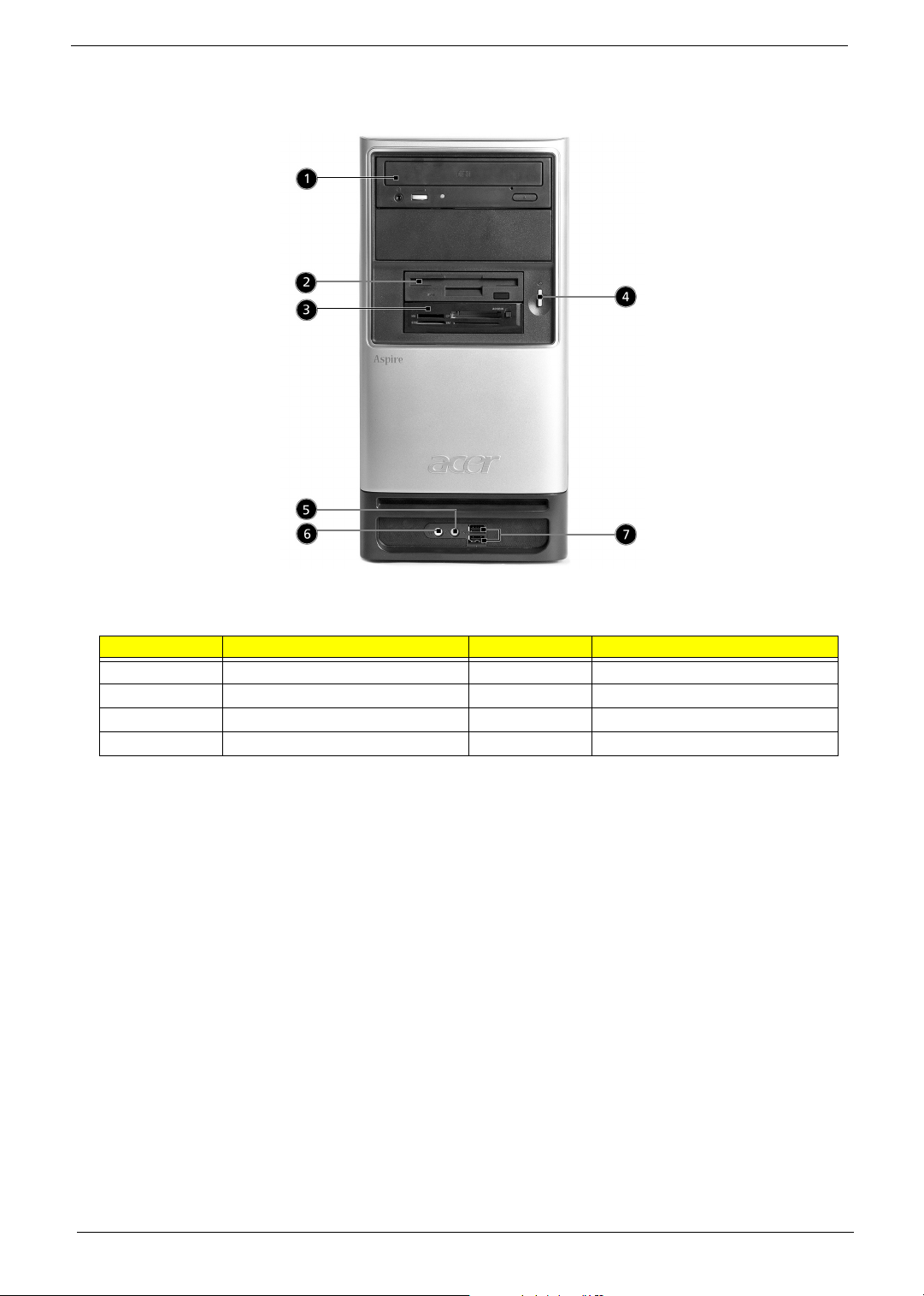
Aspire T600 Front Panel
No. Description No. Description
1 Optical Device 2 Floppy Drive
3 Multimedia Card Reader 4 Power Button
5 Microphone Jack 6 Speaker or Headphone Jack
7 USB 2.0 Ports
4 Chapter 1
Page 12
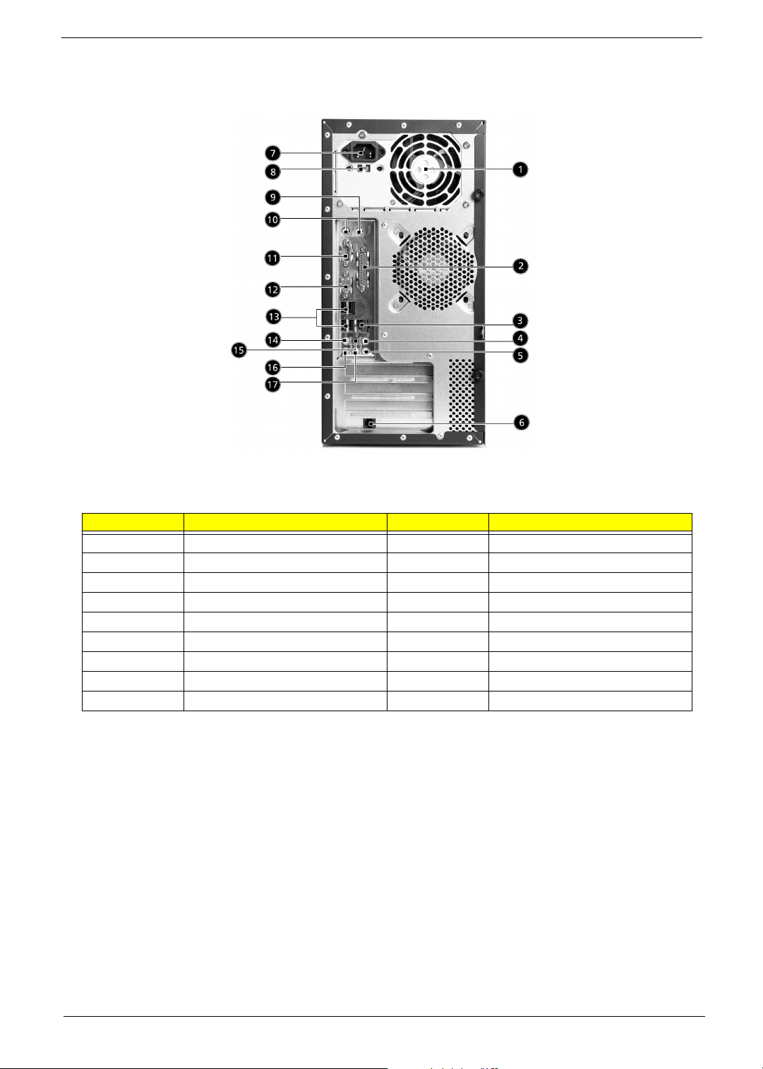
Aspire T600 Rear Panel
No. Description No. Description
1 Fan Aperture 2 Printer Connector
3 RJ-45 Ethernet Connector 4 Center-Surround/Subwoofer Jack
5 Line-in Jack 6 Modem Card (Optional)
7 Power Cord Socket 8 Voltage Selector Switch
9 Ps/2 Mouse Connector 10 PS/2 Keyboard Connector
11 Serial Port 12 VGA Port
13 USB 2.0 Ports 14 Side-surround Jack
15 Rear-surround Jack 16 Microphone-in Jack
17 Line-out / Front-surround Jack
Chapter 1 5
Page 13
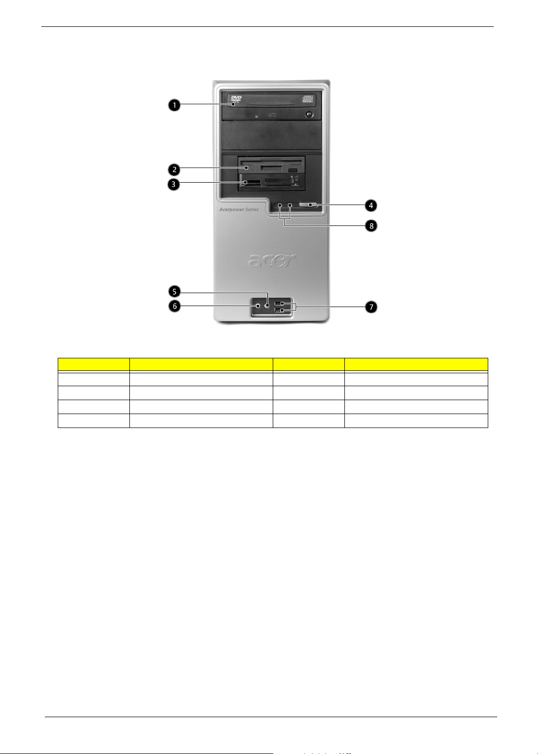
AcerPower FV Front Panel
No. Description No. Description
1 Optical Drive 2 Floppy Drive
3 Multimedia Card Reader (Optical) 4 Power Button
5 Microphone Jack 6 Speaker or Headphone Jack
7 USB 2.0 Ports 8 Indicator
6 Chapter 1
Page 14
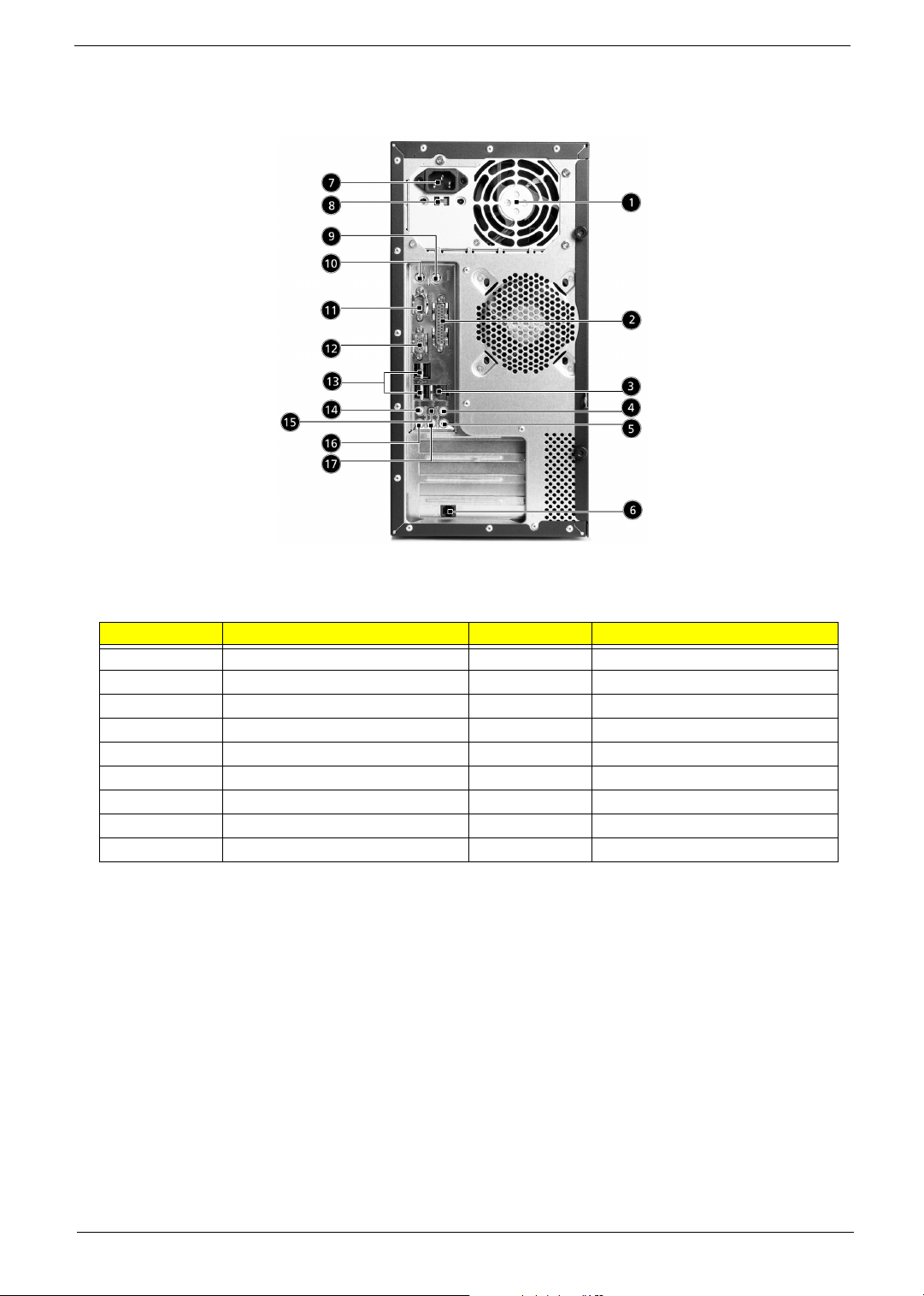
AcerPower FV Rear Panel
No. Description No. Description
1 Fan Aperture 2 Printer Connector
3 RJ-45 Ethernet Connector 4 Center-Surround/Subwoofer Jack
5 Line-in Jack 6 Modem Card (optional)
7 Power Cord Socket 8 Voltage Selector Switch
9 PS/2 Mouse Connector 10 PS/2 Keyboard Connector
11 Serial Port 12 VGA Port
13 USB 2.0 Ports 14 Side-Surround Jack
15 Rear-Surround Jack 16 Microphone-In Jack
17 Line-out / Front-Surround Jack
Chapter 1 7
Page 15
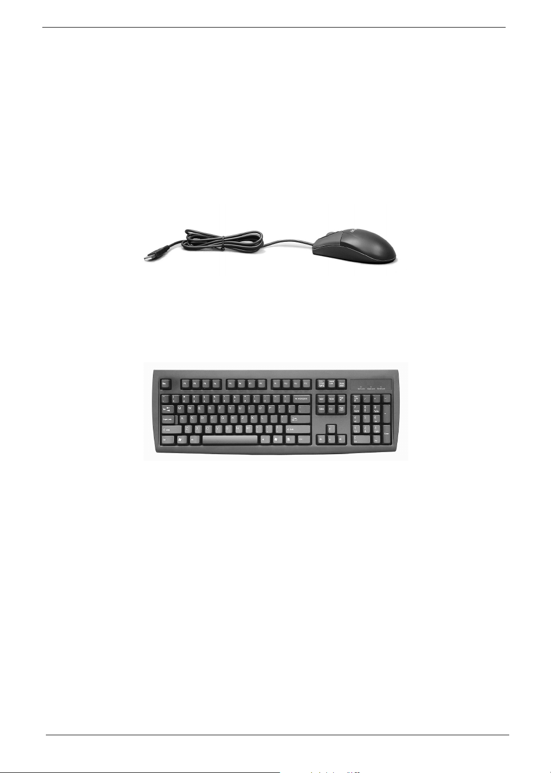
System Peripherals
The Aspire T600 and AcerPower FV computers consist of the system itself, and system peripherals, like a
mouse, a keyboard and a set of speakers (optional). This section provides a brief description of basic
system peripherals.
Mouse (PS/2 or USB, Manufacturing Option)
The included mouse is a standard two-button wheel mouse. Connect the mouse to the PS/2 mouse port
or USB port on the back panel of the system.
Keyboard (PS/2 or USB, manufacturing option)
Connect the keyboard to the PS/2 keyboard port or USB port on the back panel of the system.
8 Chapter 1
Page 16

Speakers
Note:
For systems bundled with speakers, before powering on the system, connect the speaker cable to the
audio-out (external speaker) port on the back panel of the system.
NOTE: Speakers are optional and the appearance might be different, depending on the actual product.
Chapter 1 9
Page 17
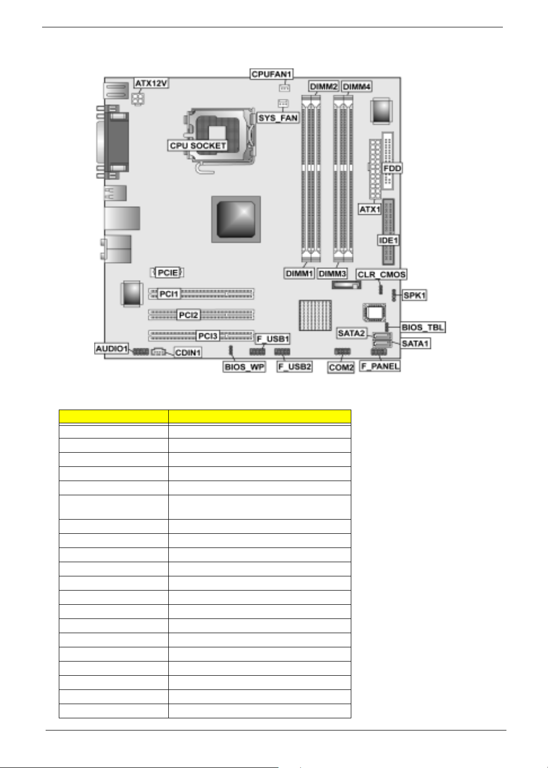
MainBoard Layout
Item Description
ATX1 Standard 24-pin ATX power connector
ATX12V ATX12V power connector
AUDIO1 Front panel audio header
BIOS_TBL BIOS TBL jumper
BIOS_WP BIOS flash protect jumper
CDIN1 Primary CD-in connector/ Auxiliary Audio input
connector
CLR_CMOS Clear CMOS jumper
COM2 Onboard serial port header
CPU SOCKET LGA775 socket for Pentium 4 CPUs
CPUFAN1 CPU cooling fan connector
DIMM1~ DIMM4 Four 184-pin DDR SDRAM slots
FDD Floppy disk drive connector
F_PANEL Front Panel switch/LED header
F_USB1 ~ F_USB2 Front panel USB headers
IDE 1 Primary IDE connector
PCI1 ~ PCI3 Three 32-bit add-on card slots
PCIE PCI Express x1 slot
SATA1 ~ SATA2 Two Serial ATA connectors
SPK1 Speaker Header
SYS_FAN System Fan Controller
10 Chapter 1
Page 18
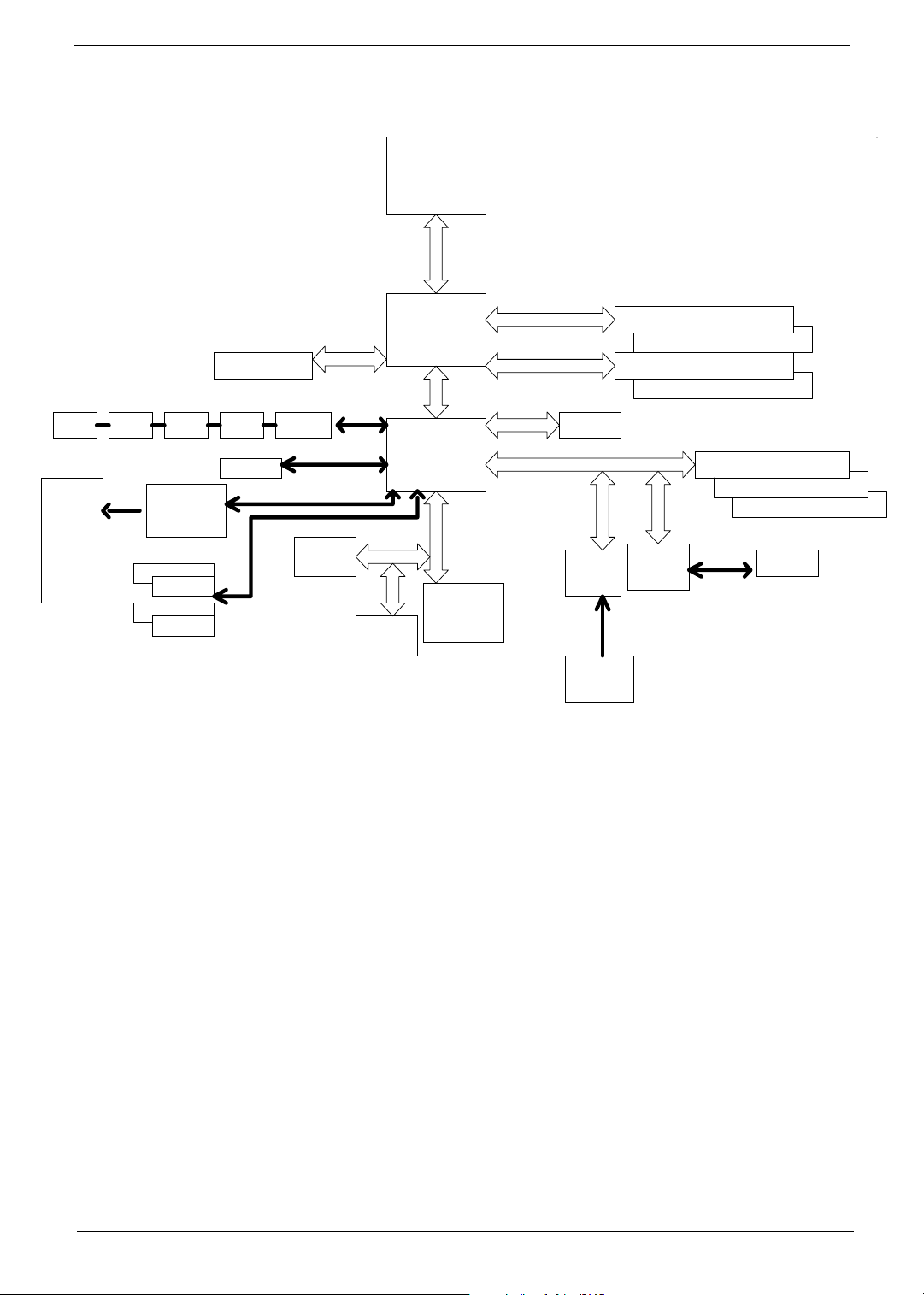
Block Diagram
y
INTEL
P4 Processor
PSC, Tejas -
LGA 775 pin
Analong Display
RAMDAC: 400MHz
Resolutions Up To 2048x1536@75Hz
USB1
2 ports
Line in
Line out
Mic in
Center/Bass out
Surround
Side-Surround
USB2
2 ports
USB3
2 ports
Audio Codec
ALC880
SATA1 7Pin
SATA2 7pin
SATA3 7Pin
SATA4 7pin
BW : 4.1GB/s @ FSB : 533MHz & Freq : 133MHz
BW : 6.4GB/s @ FSB : 800MHz & Freq : 200MHz
i915GV
VGA (G only)
USB4
2 ports
IDE1 40pin
AC' 97 & Lan I/F
BW : 150MB/s
USBLAN
8 ports
Up to Ultra ATA/100
Two IDE Channel
intel
FWH
32pin PLCC
1210pin FC-BGA
USB V2.0
INTEL
ICH6
609pin EBGA
LPC bus
TPM 1.1
INTEL
BW : 2GB/s (Support Lsoch)
Super I/O
W83627THF
128pin PQFP
SIZE : Min 128MB (ONE 256Mb X 16 Single-Sided DEVICES)
SIZE : Max 4GB (Four 512Mb X 8 Double-Sided DEVICES)
BW : 8.5GB/s @ DDR2 :400/533MHz
BW : 6.4GB/s @ DDR : 333/400MHz
DDIMM1: DDR Socket 184P
DDIMM3: DDR Socket 184P
PCIEx1
BW : 133MB/s @Freq : 33MHz
VIA 1394
(OPTION)
CONN/
HEADER
DDIMM2 : DDR Socket 184P
DDIMM4 : DDR Socket 184P
PCI1 Slot 120pin @ AD17
PCI2 Slot 120pin @ AD18
PCI3 Slot 120pin @ AD19
10/100
Lan
USBLAN
RJ45
Chapter 1 11
Page 19
Hardware Specifications and Configurations
System Board Major Chip
Item Specification
System Core Logic Intel 915GV
ICH6
Super I/O Controller W83627THF
LAN Controller ICH6
Memory Controller Build in Intel 82915GV(Champ North Bridge)
E-IDE Controller Build in ICH6 (champion South Bridge)
Audio Codec Azalia (ALC880)
LPC Controller WINBOND (W83627THF-AW)
LAN Realtek 8100C (10/100M LAN)
Keyboard Controller WINBOND (W83627THF-AW)
Processor
Item Specification
Vendor/Type Intel/Prescott and Tejas Processor
CPU Socket Type Socket-T (LGA 775)
Speed Depends on CPU, which is local configured
Bus Frequency 533/800 MHz
Voltage Processor voltage can be detected by any system without
setting any jumper
BIOS
Item Specification
BIOS code programmer AMI
BIOS ROM type Q Flash ROM
BIOS ROM size 4MB
BIOS ROM package 32-pin PLCC package
Support protocol PCIX 1.0,PCI 2.2,APM 1.2,VESA/DPMS (VBE/PM V1.1),
SMBIOS 2.3, E-IDE 1.1, ACPI 1.0b,ESCD1.03, PnP 1.0a,
Bootable CD-ROM 1.0, USB 1.1~ USB 2.0, UHCI 1.0, ANSI
ATA 3.0 ATAPI
Boot from CD-ROM feature Yes
Support to LS-120 drive Yes
Support to BIOS boot block feature Yes
BIOS Password Control Yes
NOTE: The BIOS can be overwritten/upgraded by using “AFLASH” utility (AFLASH.EXE).
12 Chapter 1
Page 20
BIOS Hotkey List
Hotkey Function Description
c Enter BIOS Setup Utility Press while the system is booting to
enter BIOS Setup Utility.
System Memory
Item Specification
Memory Slot(s) Number 4
Supported Memory Size per Slot 256 MB/ 512 MB / 1GB DDR for x8 and x16 non-ECC
DDR type module support
Supported Maximum Memory Size 4GB
Supported Memory Speed 333/400 MHz
Supported memory voltage 2.6 V
Support memory module package 184-pin DIMM
Support to parity check feature Yes
Support to Error Correction Code (ECC)
feature
Support to Registered DIMM No
Support maximum bandwidth 6.4GB/s in dual-channel interleaved mode using DDR
No
400MHz
Bus Architecture
Item Description
PCI Express 1X 1 PCS
PCI Slot 3 PCS
LAN on Board REALTEK RTL8100C
Cache Memory
Item Specification
First-Level Cache Configurations
Cache function control Enable/Disable by BIOS Setup
Second-Level Cache Configurations
The information below is only applicable to system installed with a Pentium 4 processor
Tag RAM Location On Processor
L2 Cache RAM Location On Processor
L2 Cache RAM type PBSRAM (Pipelined-burst Synchronous RAM)
L2 Cache RAM size Depends on CPU, which is local configured
L2 Cache RAM speed Full of the processor core clock frequency (Advanced Transfer Cache)
L2 Cache function control Enable/Disable by BIOS Setup
L2 Cache scheme Fixed in write-back
Chapter 1 13
Page 21
LAN Interface
Item Specification
LAN Controller Intel ICH6
LAN Chip Realteck 8100C
LAN Controller Resident Bus PCI Bus
LAN Port ONE RJ-45 on board
Design Criteria Design be worked under 10/100 Mbs environment
Function Control Reserved disable function on both hardware & BIOS side. Default is
enabled
IDE Interface
Item Specification
IDE Controller Built-in ICH6
IDE Controller Resident Bus PCI bus
Number IDE Channel 2
Supported IDE Interface E-IDE (up to PIO mode-4, DMA mode 2 and Ultra DMA-33), ANSIS
ATA rev. 3.0, ATAPI
Supports LS-120 Yes
Supports bootable CD-ROM Yes
Function Control Enable/Disable by BIOS setup
Diskette Drive Interface
Item Specification
Diskette Drive Controller W83627THF
Diskette Drive Controller Resident Bus LPC Bus
Supported Diskette Drive Formats 1.44MB, 2.88MB format and slim type diskette drive
Function Control Supports Automatic Write Protection via Software
Serial Port
Item Specification
Serial port controller W83627THF
Serial port controller resident bus LPC Bus
Number of serial port 2
Serial port location CON1,CN2
16C550 UART support Yes
Connector type 9-pin D-type female connector
Optional serial port I/O address
(via BIOS Setup)
Optional serial port IRQ
(via BIOS Setup)
3F8h
2F8h
3E8h
2E8h
IRQ4
14 Chapter 1
Page 22
System LED Definition
LED Definition
Power State LED
S0 Green Steady
S1/S3 Amber Steady
S4/S5 Off
HDD State LED
IDE Active Green Blinking
IDE Idle Off
LAN State LED
LAN Active Green Blinking
LAN Idle Off
USB Port
Item Specification
USB Controller ICH6
Connectors Quantity 8
T Rear Connectors 4
T On-board Header 4
T 2 for front daughter board (Pin: 2x5 Intel FPIO)
T 1 for Media card reader (Pin: 1*5)
Data Transfer Rate Support USB 2.0/1.1
Universal HCI USB 2.0 ports for serial transfers at 480Mbits/Sec. Max. Legacy
Keyboard and Mouse support
Memory Address Map
Address Size Function
0000000 - 009FFFF 640 KB System Memory Onboard DRAM
00A0000-00BFFFF 128 KB Video RAM Reserved for Graphics Display
Buffer
Non-Cacheable
00C0000-00CFFFF 32 KB I/O Expansion ROM Reserved for ROM on I/O
Adapters
00D0000-00D3FFF 16 KB I/O Expansion ROM Reserved for ROM on I/O
Adapters
00D4000-00D7FFF 16 KB I/O Expansion ROM Reserved for ROM on I/O
Adapters
00D8000-00DBFFF 16 KB I/O Expansion ROM Reserved for ROM on I/O
Adapters
00DC000-00DFFFF 16 KB I/O Expansion ROM Reserved for ROM on I/O
Adapters
00E0000-00E7FFF 32 KB for SCSI BIOS Reserved for SCSI BIOS
00E8000-00EFFFF 32 KB Reserved Onboard
00F0000-00FFFFF 64 KB BIOS System ROM BIOS (ROM)
System RAM BIOS (DRAM)
Chapter 1 15
Page 23
Dual Channel
Aspire T600/AcerPower FV support the Dual Channel Technology. After operating the dual channel
technology, the bandwidth of memory bus will add double up to 6.4GB/s.
Aspire T600/AcerPower FV inculde 4 DIMM sockets, and each channel has two DIMM sockets as following:
T Channel A : DDR1, DDR2
T Channel B : DDR3 , DDR4
If you want to operate the Dual Channel Technology, please note the following explanations due to
the limitation of Intel chipset specifications.
Memory Number Description
1 Only one DDR memory module is
installed ?
2 Two DDR memory modules are
installed ( the same memory size and
type) ?
3 Three DDR memory modules are
installed ?
4 Four DDR memory modules are
installed ?
The Dual Channel Technology can’t operate when only one DDR
memory module is installed.
The Dual Channel Technology will operate when two memory
modules are inserted individually into Channel A and B. If you
install two memory modules in the same channel, the Dual
Channel Technology will not operate.
Pleae note that the Dual Channel Technology will not operate
when three DDR memory modules are installed; part of them will
not be detected.
If you install four memory modules at the same time, the Dual
Channel Technology will operate only when those modules have
the same size and type.
NOTE: We strongly recommend user to slot two DDR memory modules into the DIMMs with the same color in
order for Dual Channel Technology to work.
The following tables include all memory-installed combination types:
Dual Channel Technology (DS: Double Side, SS: Single Side)
DDR1 DDR2 DDR3 DDR4
2 memory modules DS/SS X DS/SS X
X DS/SS X DS/SS
4 memory modules DS/SS DS/SS DS/SS DS/SS
Don’t operate Dual Channel Technology (DS:Double Side, SS: Single Side)
DDR1 DDR2 DDR3 DDR4
DS/SSXXX
X DS/SS X X
1 memory module
2 memory module DS/SS DS/SS X X
3 memory module
XXDS/SSX
XXXDS/SS
XXDS/SSDS/SS
DS/SS DS/SS DS/SS X
DS/SS DS/SS X DS/SS
DS/SS X DS/SS DS/SS
X DS/SS DS/SS DS/SS
16 Chapter 1
Page 24

Memory Address Map
Address Size Function
0100000-0F9FFFF System Memory Onboard DRAM
0FA0000-0FFFFFF 384 KB I/O Card Memory Reserved for Memory Map
I/O Card
Non-Cacheable
1000000-FFFFFFF System Memory Onboard DRAM
PCI INTx# and IDSEL Assignment Map
PCI INTx # PCI Devices Device IDSEL: ADxx
INTA# ADIMM-slot N
INTB# PCI-Slot1 AD16
INTC# PCI-Slot2 AD17
PCI Slot IRQ Routing Map
PCI INTX# INTA INTB INTC INTD Bus Mastering
PCI slot 1 INTE INTCD INTC INTA Enabled
PCI slot 2 INTD INTC INTA INTE Enabled
PCI slot 3 INTFJ INTGJ INTHJ INTEJ Enabled
I/O Address Map
Hex Range Devices
000-01F
020-021
040-043
060-060
061-061
070-071
080-08F
0A0-0A1
0C0-0DF
0F0-0FF
170-177
1F0-1F7
278-27F
2F8-2FF
378-37F
3F0-3F5
3F6-3F6
3F7-3F7
3F8-3FF
0CF8
0CFC
778-77A
DMA Controller-1
Interrupt Controller-1
System Timer
Keyboard Controller 8742
System Speaker
CMOS RAM Address and Real Time Clock
DMA Page Register
Interrupt Controller-2
DMA Controller-2
Math Co-Processor
Secondary IDE
Primary IDE
Parallel Printer Port 2
Serial Asynchronous Port 2
Parallel Printer Port 1
Floppy Disk Controller
Secondary IDE
Primary IDE
Serial Asynchronous Port 1
Configuration Address Register
Configuration Data Register
Parallel Printer Port 1
Chapter 1 17
Page 25
IRQ Assignment Map
IRQx System Devices Add-On-Card Devices
IRQ0 Timer N
IRQ1 Keyboard N
IRQ2 Reserved N
IRQ3 Serial Port 2 Reserved
IRQ4 Serial Port 1 Reserved
IRQ5 Reserved Reserved
IRQ6 Floppy Disk Reserved
IRQ7 Parallel Port Reserved
IRQ8 Real Time Clock N
IRQ9 N Reserved
IRQ10 N Reserved
IRQ11 N Reserved
IRQ12 PS/2 Mouse Reserved
IRQ13 Numeric Processor N
IRQ14 Embedded Hard Disk Reserved
IRQ15 Reserved Reserved
NOTE: N - Not be used
DRQ Assignment Map
DRQx System Devices Add-On-Card Devices
DRQ0 N Reserved
DRQ1 N Reserved
DRQ2 FDD N
DRQ3 N Reserved
DRQ4 Cascade N
DRQ5 N Reserved
DRQ6 N Reserved
DRQ7 N Reserved
NOTE: N - Not be used
Environmental Requirements
Item Specifications
Temperature
Operating
Non-operating
o
C to +35oC
+5
-20oC ~ +60°C (Packed) -10oC~+60oC (un-packed)
Humidity
Operating 15% to 80% RH, non-condensing
Non-operating
10% to 90% RH, non-condensing at 40
o
C
Vibration
18 Chapter 1
Page 26

Environmental Requirements
Item Specifications
Vibration unpacked 5~500 Hz, 2.20g RMS random, 10 minutes per axis in all 3 axes
Vibration packed 5~500 Hz, 1.09g RMS random, 1 hour per axis in all 3 axes
Shock operating Half sine, 2 g 11m seconds
Mechanical Specifications
Item Specification
Dimensions(main footprint) 180(w)x360(H)x420(D)mm
Chapter 1 19
Page 27

Power Management Function (ACPI support function)
Device Standby Mode
T Independent power management timer for hard disk drive devices
(0-15 minutes, time step=1 minute).
T Hard disk drive goes into Standby mode (for ATA standard interface).
T Disable V-sync to control the VESA DPMS monitor.
T Resume method: device activated (Keyboard for DOS, keyboard & mouse for Windows).
T Resume recovery time: 3-5 sec.
Global Standby Mode
T Global power management timer (2-120 minutes, time step=10 minute).
T Hard disk drive goes into Standby mode (for ATA standard interface).
T Disable H-sync and V-sync signals to control the VESA DPMS monitor.
T Resume method: Return to original state by pushing external switch button, modem ring in,
keyboard and mouse for APM mode.
T Resume recovery time: 7-10 sec.
Suspend Mode
T Independent power management timer (2-120 minutes, time step=10 minutes) or pushing external
switch button.
T CPU goes into SMM.
T CPU asserts STPCLK# and goes into the Stop Grant State.
T LED on the panel turns amber colour.
T Hard disk drive goes into SLEEP mode (for ATA standard interface).
T Disable H-sync and V-sync signals to control the VESA DPMS monitor.
T Ultra I/O and VGA chip go into power saving mode.
T Resume method: Return to original state by pushing external switch button, modem ring in,
keyboard and mouse for APM mode.
T Return to original state by pushing external switch button, modem ring in and USB keyboard for
ACPI mode.
ACPI
T ACPI specification 1.0b.
T S0, S1, S3 and S5 sleep state support.
T On board device power management support.
T On board device configuration support.
20 Chapter 1
Page 28
Chapter 2
System Utilities
BIOS (Basic Input and Output System) includes a CMOS SETUP utility which allows user to
configure required setting or to active certain system features.
The CMOS SETUP saves the configuration in the CMOS SRAM of the mainboard. When the power is turned
off, the battery on the mainboard supplies the necessary power to the CMOS SRAM.
When the power is turned on, pushing the <Del> button during the BIOS POST (Power-On Self Test) will take
you to the CMOS SETUP screen. When setting up BIOS for the first time, it is recommended that you save
the current BIOS to a disk in the event that BIOS needs to be reset to its original settings.
Q-Flash allows the user to quickly and easily update or backup BIOS without entering the operating system.
BIOS is a Window s-based utility that doesn’t required users to boot to DOS before upgrading BIOS but
directly download and update BIOS from the Internet.
Control Keys
Item Description
wxyz Move to selection
e Main Menu: Quit and not save changes into CMOS Status Page Setup
Menu and Option Page Setup Menu, Exit current page and return to
Main Menu.
{ Increase the numeric value or make changes
} Decrease the numeric value or make changes
l Displays a screen that describes all key functions
t Loads an optimized setting for better performance
u Saves the current configuration and exits setup
Chapter 2 21
Page 29

Entering Setup
Once enter Award BIOS CMOS Setup Utility, the Main Menu (as figure below) will appear on the screen.
Use arrow keys to select among the items and press <Enter> to accept or enter the sub-menu.
Parameter Description
Product Information To introduce the Product Name, System P/N and Mainboard ID...etc
Standard CMOS Features This setup page includes all the items in standard compatible BIOS
Advanced BIOS Features This setup page includes all the items of Award special enhanced
features
Advacned Chipset Features The values for the chipset can be changed through this menu, and the
system performance can be optimized
Integrated Peripherals This setup page includes all onboard peripherals
Power Management Setup This setup page includes all the items of Green function features
PnP/PCI Configuration This setup page includes all configurations of PCI&PnP ISA resources
PC Health Status This setup page is the System auto detect Temperature, voltage, fan
and speed
Frequency Control Frequency and voltage settings can be loaded through this menu
Set Supervisor Password Change, set or disable password. It allows you to limit access to the
system and Setup, or just to Setup
Load Default Settings These parameter settings can be loaded through this menu, however,
the stable default values may be affected
Save & Exit Setup Save CMOS value settings to CMOS and exit setup
Exit Without Saving Abandon all CMOS value changes and exit setup
22 Chapter 2
Page 30

Product Information
The screen below appears if you select Product Information from the main menu.
The Product Information menu contains gerenal data about the system, such as the product name, serial
number, BIOS version, etc. These information is necessary for troubleshooting (maybe required when
asking for technical support).
Parameter Description
Product Name Displays the model name of your system
System S/N Displays your system’s serial number
Main Board ID Displays the main board’s indentification number
System BIOS Version Specifies the version of BIOS utility
SMBIOS Version The System Management Interface (SM) BIOS allows you to check the system
hardware components without actually opening the system. Hardware checking
is done via software during start up. This parameter specifies the version of the
SMBIOS utility installed in your system
BIOS Release Date MM/DD/YYYY
Chapter 2 23
Page 31

Standard CMOS Features
Select Standard CMOS Features from the main menu to configure some basic parameters in your system.
The following screen shows the Standard CMOS Features menu:
The following table describes the parameters found in this menu:
Parameter Description Options
Date Lets you set the date following the weekday-
month-day-year format
Time Lets you set the time following the hour-minute-
second format
ATA/IDE Configuration The ATA/IDE option can be configured as “Disabled”, “Compatible (default)” and “Enhanced” in
the BIOS configuration. Windows* 98SE and Windows* Me operating systems do not support
Enhanced mode IDE/Serial ATA resources for more than four devices. If the ATA/IDE option is
set to Enhanced mode, the operating installation will not be able to recognize the drive, and the
installation will fail. Before installing 98SE or Me, the ATA/IDE configuration must be changed
from Enhanced to Legacy mode.
Week : from Sun. to Sat., determined by
BIOS and is display only
Month : from Jan. through Dec.
Day : from 1 to 31 ( or the maximum allowed
in the month)
Year : from 1999 to 2098
The items format is <hour>
<minut><second>. The time is calculated
base on the 24-hour military-time clock. For
example, 1 p.m. is 13:00:00
24 Chapter 2
Page 32

Parameter Description Options
Legacy IDE Channels Use this item to set up the primary and
secondary sequence of IDE channels and SATA
channel. If set ATA/IDE Configuration to
Compatible mode and IDE channels to SATA Pri/
PATA Sec, users can only plug in SATA devices
on SATA1 and SATA2; if set ATA/IDE
Configuration to Compatible mode and IDE
channels as SATA Sec/PATA Pri, users can only
plug in SATA devices on SATA3 and SATA4
Primary/Second IDE
Master/Slave
Drive A Allows you to configure you floppy drive A 360K, 5.25” : 5.25 inch PC type standard
Allows you to configure the hard disk drive
connected to the master or slave port of IDE
channel. To enter the IDE Primary/Secondary
Master/Slave setup, press [Enter] .
N/A
N/A
drive ; 360Kbyte capacity
1.2M, 5.25” : 5.25 inch AT-type high-density
drive; 1.2M byte capacity (3.5 inch when 3
Mode is Enabled)
720K, 3.5” : 3.5 inch double-sided drive;
720Kbyte capacity
1.44M, 3.5” : 3.5 inch double-sided drive;
1.44Mbyte capacity
2.88M, 3.5” : 3.5 inch double-sided drive;
2.88Mbyte capacity
Chapter 2 25
Page 33

Advanced BIOS Features
The following screen shows the Advanced BIOS Features:
Parameter Description Options
Virus Warning When enabled, this item provides protection
against viruses that try to write to the boot
sector and partition table of your hard disk drive.
You need to disable this item when installing an
operating system. We recommend that you
enable this item as soon as you have installed
an operating system.
Silent Boot This is to switch 1st screen logo (default Acer’
logo)
Configuration Table This is to select if system configuration shown
Quick Power on Self Test Enable this item to shorten the power on testing
First / Second / Third Boot
Device
Boot Other Device When enabled, the system searches all other
Boot Up NumLock Status This item defines if the keyboard Num Lock key
APIC Mode This option enables/disables APIC (Advanced
by 2nd screen or not.
(POST) and have your system start up faster.
You might like to enable this item after you
areconfident that your system hardware is
operating smoothly.
The items allow you to set the sequence of boot
device where BIOS attempts to load the disk
operating system
possible locations for an operating system if it
fails to find one in the devices specified under
the First, Second, and Third boot devices.
is active when your system is started.
Programmable Interrupt Controller)
functionality. The APIC is an Intel chip that
provides symmetric multiprocessing (SMP) for
its Pentium systems.
Diabled
Enabled
Disabled
Enabled
Disabled
Enabled
Disabled
Enabled
Floppy, LS120, Hard Disk, CD-ROM,
ZIP, USB-FDD, USB-ZIP, USbCDROM, USB-HDD, LAN, Disabled
Disabled
Enabled
On
Off
Disabled
Enabled
26 Chapter 2
Page 34

Removable Drives
Chapter 2 27
Page 35

Advanced Chipset Features
The advanced chipset features setup option is used to change the values of the chipset registers. These
registers control most of the system options in the computer.
Parameter Description
DRAM Frequency This item determines frequency of DRAM memory.
Configure DRAM Timing by
SPD
DRAM CAS# Latency This item determines the operation of DRAM memory CAS (column address
DRAM RAS# to CAS# Delay This field lets you insert a timing delay between the CAS and RAS strobe
DRAM RAS# Precharge Select the number of CPU clocks allocated for the Row Address Strobe (RAS#)
DRAM RAS# Activate to
Precharge
Enables you to select the CAS latency time in HCLKs of 2, 2.5, or 3. The value
is set at the factory depending on the DRAM installed. Do not change the values
in this field unless you change specifications of the installed DRAM or the
installed CPU.
strobe). It is recommended that you leave this item at the default value. The 3T
setting requires faster memory that specifically supports this mode. Please be
noted that the item would be hidden when set Configure DRAM Timing by SPD
to Enabled.
signals, used when DRAMis written to, read from, or refreshed. Disabled gives
faster performance; and Enabled gives more stable performance. Please be
noted that the item would be hidden when set Configure DRAM Timing by SPD
to Enabled.
signal to accumulate its charge before the DRAM is refreshed. If insufficient
time isallowed, refresh may be incomplete and data lost. Please be noted that
the item would be hidden when set Configure DRAM Timing by SPD to Enabled.
The precharge time is the number of cycles it takes for DRAM to accumulate its
charge before refresh. Please be noted that the item would be hidden when set
Configure DRAM Timing by SPD to Enabled.
28 Chapter 2
Page 36

Parameter Description
Init Display First Use this item to specify whether your graphics adapter is installed in one of the
PCI slots or is integrated on the mainboard
VGA Share Memory This item shows the VGA memory size borrowed from main memory capacity.
Aperture Size Select This item defines the size of the aperture if you use an AGP graphics adapter.
PEG Port This item enables or disables the PCI Express Graphics port function.
The AGP aperture refers to a section of the PCI memory address range used for
graphics memory. We recommend that you leave this item at the default value.
Chapter 2 29
Page 37

Integrated Peripherals
Parameter Description Options
USB 2.0 Controller Enable this item if the system supports USB 2.0 Enabled : Enable USB 2.0
Controller
Disabled : Disable USB 2.0
Controller
USB Function This item is used to enable or disable the on-chip
USB
Legacy USB Support This item allows you to enable or disable Legacy
USB support.
Onboard AUDIO Function Enabling the on-die audio if no add-on PCI audio
device
Onboard LAN Function Enables and disables the onboard LAN Enabled
LAN Boot ROM Support This function decide whether to invoke the boot
ROM of the onboard LAN chip
Serial Port 1/2 Address This option is used to assign the I/O address and
interrupt request (IRQ) for onboard serial port 1
or 2
Enabled
Disabled
Enabled
Disabled
Enabled
Disabled
Disabled
Enabled : Enable this function
Disabled : Disable this function
Auto : BIOS will automatically
setup the port 1 or 2 address
3F8/IRQ4
2F8/IRQ3
3E8/IRQ4
2E8/IRQ3
Diabled : Disable onboard Serial
port 1 or 2
30 Chapter 2
Page 38

Parameter Description Options
Parallel Port Address Use this item to enable or disable the onboard
Parallel port, and to assign a port address.
Parallel Port Mode Enables you to set data transfer protocol for your
parallel port.
There are four options: SPP (Standard Parallel
Port),
EPP(Enhanced Parallel Port), ECP(Extended
Capabilities Port) and ECP+EPP.
SPP allows data output only.
Port (ECP) and Enhanced Parallel Port (EPP)
are bi-Extended Capabilities directional modes,
allowing both data input and output. ECP and
EPP modes are only supported with EPP and
ECP aware peripherals.
ECP Mode DMA Channel When the onboard parallel port is set to ECP
mode,the parallel port can use DMA 3 or DMA 1.
Parallel Port IRQ This item assigns either IRQ 5 or 7 to the parallel
port
N/A
SPP
EPP
ECP
ECP+EPP
1
3
N/A
Chapter 2 31
Page 39

Power Management Setup
The Power Management menu lets you configure your system to most effectively save energy while operating
in a manner consistent with your own style of computer use.
The following screen shows the Power Management parameters and their default settings:
Parameter Description Options
ACPI Suspend Type This item specifies the power saving modes for ACPI
function. S1(POS): The S1 sleep mode is a low power
state. In this state, no system context (CPU or chipset)
is lost and hardware maintains all system context. S3
(STR): The S3 sleep mode is s power-down state in
which power is supplied only to essential components
such as main memory and wake-capable devices and
all system context is saved to main memory. The
information stored in memory will be used to restore
the PC to the previous state when an wake-up event
occurs.
Video Off In Suspend This option defines if the video is powered down when
the system is put into suspend mode.
HDD Power Down This option lets you specify the IDE HDD idle time
before the device enters the power down state. This
item is independent from the power states previously
described in this section (Standby and Suspend).
Soft-off by PWR-BTTN This feature allows users to configure the power button
function.
S1 (POS) : Set ACPI suspend
type to S1/POS(Power On
Suspend).
S3 (STR) : Set ACPI suspend
type to S3/STR
Disabled
Enabled
Disabled
1~15 Mins
Instand-off : Press down
button then power off instantly
Delay 4 Sec. : Press power
button 4 sec. to power off.
Enter suspend if button is
pressed less than 4 sec.
32 Chapter 2
Page 40

Parameter Description Options
POWER After PWR-Fail This item enables your computer to automatically
restart or return to its former operating status after
power returns from a power failure.
Power On by Ring An input signal on the serial Ring Indicator (RI) line (in
other words, an incoming call on the modem) awakens
the system from a soft off state.
Wake-Up by PCI Card This option determines the system wakup by PCI card Disabled
USB KB Wake UP from S3 USB Keyboard wakeup from S3 (tandyb status) Disabled
PS/2 Keyboard Wakeup Set this via keyboard to power on the system Password : Enter from 15
PS/2 Mouse Wakeup Set this via mouse to power on the system Disabled : Disable this
Resume by Alarm You can set “Resume by Alarm” item to enabled and
key in Data/Time to power on system
Former-Sts
Disabled : Disable Power On
by Ring function
Enabled : Enable Power On
by Ring function
Enabled
Enabled
characters to set the
Keyboard Power On
Password
Disabled : Disable this
function
Keyboard 98 : If your
keyboard have “Power Key”
button, you can press the key
to power on the system
function
Double Click : Double click on
PS/2 mouse left button to
power on the system
Disabled : Disable this
function
Enabled : Enable alarm
function to Power On system
If RTC Alarm Lead To Power
On is Enabled.
Date (of Month) Alarm :
Everyday, 1~31
Time (hh:mm:ss) Alarm:
(0.~23):(0~59):(0~59)
Chapter 2 33
Page 41

PnP/PCI Configuration
Parameter Description Options
PCI/VGA Palette Snoop Disabled - Data read or written by the CPU
is only directed to the PCI VGA device’s
palette registers.
Enabled - Data read or written by the CPU is
directed to both the PCI VGA device’s
palette registers and the ISA VGA device’s
palette registers,permitting the palette
registers of both VGA devices to be
identical.
Disabled
Enabled
34 Chapter 2
Page 42

PC Health Status
The following table describes the parameters found in this menu:
Parameter Description
CPU Shutdown Temperature Enables you to set the maximum temperature the
system can reach before powering down.
Current CPU Temperature Detect CPU Temperature automatically
Current SYSTEM Temperature Detect SYSTEM Temperature automatically
Current CPU / SYSTEM FAN Speed
(RPM)
Detect CPU/SYSTEM Fan Speed status automatically
o
C/140o F
60
o
65
C/149oF
o
70
C/158o F
Disabled
Chapter 2 35
Page 43

Frequency Control
The following table describes the parameters found in this menu:
Parameter Description Option
Ratio CMOS Setting This item sets the ratio between CPU Core Clock
and the FSB Frequency. Users please note that if
a invalid ratio has been entered to this field, BIOS
will restore it to previous state.
Auto Detect DIMM / PCI Clk When this item is enabled, BIOS will disable the
clock signal of free DIMM and PCI slots.
Spread Spectrum If you enable spread spectrum, it can significantly
reduce the EMI (Elector Magnetic Interference)
generated by the system.
14
Enabled
Disabled
Enabled
Disabled
36 Chapter 2
Page 44

Set Supervisor Password
When this function is selected, the following message appears at the center of the screen to assist you in
creating a password.
Type the password, up to eight characters, and press <Enter>. The password typed now will clear any
previously entered password from CMOS memory. You will be asked to confirm the password. Type the
password again and press <Enter>. You may also press <Esc> to abort the selection.
To disable password, just press <Enter> when you are prompted to enter password. A message will confirm
the password being disabled. Once the password is disabled, the system will boot and you can enter BIOS
Setup freely.
If you have selected “System” in “Security Option” of “BIOS Features Setup” menu, you will be prompted for
the password every time the system reboots or any time you try to enter BIOS Setup.
If you have selected “Setup” at “Security Option” from “BIOS Features Setup” menu, you will be prompted for
the password only when you enter BIOS Setup.
Supervisor Password has higher priority than User Password. You can use Supervisor Password when
booting the system or entering BIOS Setup to modify all settings.
Chapter 2 37
Page 45

Save & Exit Setup
Highlight this item and press <Enter> to save the changes that you have made in the Setup Utility and exit the
Setup Utility.
When the Save and Exit dialog box appears, press <Y> to save and exit, or press <N> to return to the main
menu.
38 Chapter 2
Page 46

Exit Without Saving
Highlight this item and press <Enter> to discard any changes that you have made in the Setup Utility and exit
the Setup Utility.
When the Exit Without Saving dialog box appears, press <Y> to discard changes and exit, or press <N> to
return to the main menu.
NOTE: If you have made settings that you do not want to save, use the "Exit Without Saving" item and press
<Y> to discard any changes you have made.
Chapter 2 39
Page 47

Machine Disassembly and Replacement
This chapter contains step-by-step procedures on how to disassemble the Aspire T600/AcerPower FV
desktop computer for maintenance and troubleshooting.
NOTE: The screws for the different components vary in size. During the disassembly process, group the
screws with the corresponding components to avoid mismatches when putting back the components.
Chapter 3
Chapter 3 40
Page 48

General Information
Before You Begin
Before proceeding with the disassembly procedure, make sure that you do the following:
1. Turn off the power to the system and all peripherals.
2. Unplug the AC adapter and all power and signal cables from the system.
Chapter 3 41
Page 49

Disassembling the Aspire T600
Opening the Housing
This section tells you how to open the housing cover when you need to install additional components inside
the system unit.
CAUTION: Before you proceed, make sure that you have turned off the system and all peripherals connected
to it.
Opening the Housing
1. Place the system unit on a flat, steady surface..
2. Turn the housing back, and remove the two screws as shown here.
3. Slide the both side doors out. Then remove it.
Removing the Front Panel
1. Remove the front panel as the picture shows carefully.
.
42 Chapter 3
Page 50

Removing the CD-ROM/FDD/HDD
1. Push on black track, and pull out CD-ROM as shown here.
2. Push on black track, and pull out FDD as shown here.
3. Push on black track, and pull out HDD as shown here..
Removing the System Fan
1. Remove the four screws as red circle shown. Then remove the system fan.
Removing the Cables
1. Disconnect the CD-ROM power cables, IDE cable.
2. Disconnect the IDE cable and power cables from the rear the FDD.
3. Disconnect the power cable and Serial ATA cable from the HDD.
Chapter 3 43
Page 51

4. Disconnect system fan cable (as highlight in red) and CPU fan cable (as highlight in yellow).
5. Disconnect the floppy cable.
6. Disconnect the IDE cable.
7. Disconnect the Serial ATA cable.
8. Disconnect the Power/HDD LED Cable and Power Switch Cable.
Removing the Power Supply
1. Remove the main power connector as shown here.
2. Remove the CPU power connector as shown here.
3. Remove the four screws as red circle shown. Then remove power supply.
Removing the TV Card
1. Pull out the CD-IN from TV card.
2. Remove the screws as shown here. then pull out the TV card.
44 Chapter 3
Page 52

Removing the Modem Card
1. Remove the screws as shown here, pull out the modem card.
Removing the Memory
1. Pull out the memory1, memory2, memory3 and memory4. Then remove it as shown here. .
Removing the Heatsink and CPU
1. Remove the four screws as shown here, then remove heatsink module.
2. Pull the CPU bar up to 90 degrees and remove the CPU then press down the CPU bar to the end.
Chapter 3 45
Page 53

Removing the MainBoard
1. Remove the eight screws as red circle shown. Then remove the mainboard.
Removing the Daughter Board
1. Remove the screw as shown here.
2. Detach the USB cable and audio cable from the daughter board.
46 Chapter 3
Page 54

Disassembling the AcerPower FV
Opening the Housing
This section tells you how to open the housing cover when you need to install additional components inside
the system unit.
CAUTION: Before you proceed, make sure that you have turned off the system and all peripherals connected
to it.
Opening the Housing
1. Place the system unit on a flat, steady surface.
2. Turn the housing back, and remove the two screws as shown here.
3. Slide the both side doors out. Then remove them.
Removing the Front Panel
Remove the bezel by following the instruction below.
Chapter 3 47
Page 55

Removing the Cables
1. Disconnect the CD-ROM power cables, IDE cable.
2. Disconnect the IDE cable and power cables from the rear the FDD.
3. Disconnect the power cable and Serial ATA cable from the HDD.
4. Disconnect system fan cable (as red circle) and CPU fan cable (as yellow circle).
5. Disconnect the floppy cable.
6. Disconnect the IDE cable.
7. Disconnect the Serial ATA cable.
8. Disconnect the Power/HDD LED Cable and Power Switch Cable.
48 Chapter 3
Page 56

Removing the CD-ROM, FDD and HDD
1. Push on black track, and pull out CD-ROM as shown here.
2. Push on black track, and pull out FDD as shown here.
3. Push on black track, and pull out HDD as shown here.
Removing the System Fan
Remove the four screws as red circle shown. Then remove the system fan.
Removing the Power Supply
1. Remove the main power connector as shown here.
2. Remove the CPU power connector as shown here.
3. Remove the four screws as red circle shown. Then remove power supply.
Chapter 3 49
Page 57

Removing the TV Card
1. Pull out the CD-IN from TV card.
2. Remove the screws as shown here. then pull out the TV card.
Removing the Modem Card
Remove the screws as shown here, pull out the modem card.
Removing the Cables
1. Disconnect the USB Cable.
2. Disconnect the Serial ATA cable.
3. Disconnect the Audio Cable.
Removing the Memory
Remove the four screws as shown here, then remove heatsink module.
50 Chapter 3
Page 58

Removing the Heatsink and CPU
1. Remove the four screws as shown here, then remove heatsink module.
2. Pull the CPU bar up to 90 degrees and remove the CPU then press down the CPU bar to the end.
Removing the Mainboard
Remove the eight screws as red circle shown. Then remove the mainboard.
Removing the Daughter Board
1. Remove the screw as shown here.
2. Detach the USB cable and audio cable from the daughter board.
Chapter 3 51
Page 59

Troubleshooting
This chapter provides troubleshooting information for the Aspire T600/AcerPower FV.
T Power-On Self-Test (POST)
T Index of Error Message
T Index of Error Symptoms
T Undetermined Problems
Chapter 4
Chapter 4 52
Page 60

Power-On Self-Test (POST)
Each time you turn on the system, the Power-on Self Test (POST) is initiated. Several items are tested during
POST, but is for the most part transparent to the user.
The Power-On Self Test (POST) is a BIOS procedure that boots the system, initializes and diagnoses the
system components, and controls the operation of the power-on password option. If POST discovers errors in
system operations at power-on, it displays error messages on screen, generates a check point code at port
80h or even halts the system if the error is fatal.
The main components on the main board that must be diagnosed and/or initialized by POST to ensure system
functionality are as follows:
T Microprocessor with built-in numeric co-processor and cache memory subsystem
T Direct Memory Access (DMA) controller
T Interrupt system
T Three programmable timers
T ROM subsystem
T RAM subsystem
T CMOS RAM subsystem and real time clock/calendar with battery backup
T Onboard parallel interface controller
T Embedded hard disk interface and one diskette drive interface
T Keyboard and auxiliary device controllers
T 1.44M floppy controller
T I/O ports
T One parallel port
T One PS/2-compatible mouse port
T One PS/2-compatible keyboard port
NOTE: When Post executes a task, it uses a series of preset numbers called check points to be latched at
port 80h, indicating the stages it is currently running. This latch can be read and shown on a debug board.
The following table describes the BIOS common tasks carried out by POST. Each task is denoted by an
unique check point number. For other unique check point numbers that are not listed in the table, refer to the
corresponding product service guide.
Post Checkpoints List: The list may vary accordingly depending on your BIOS
.
Checkpoint Description
CFh Test CMOS R/W functionality
C0h Early chipset initialization:
-Disable shadow RAM
-Disable L2 cache (socket 7 or below)
-Program basic chipset registers
C1h Detect memory
-Auto-detection of DRAM size, type and ECC.
-Auto-detection of L2 cache (socket 7 or below)
C3h Expand compressed BIOS code to DRAM
C5h Call chipset hook to copy BIOS back to E000 & F000 shadow RAM.
01h Expand the Xgroup codes locating in physical address 1000:0
02h Reserved
53 Chapter 4
Page 61

.
Checkpoint Description
03h Initial Superio_Early _Init switch
04h Reserved
05h 1. Blank out screen
2. Clear CMOS error flag
06h Reserved
07h 1. Clear 8042 interface
2. Initialize 8042 self-test
08h 1. Test special keyboard controller for Winbond 977 series Super I/O chips.
2. Enable keyboard interface.
09h Reserved
0Ah 1. Disable PS/2 mouse interface (optional)
2. Auto detect ports for keyboard & mouse followed by a port & interface swap
(optional).
3. Reset keyboard for Winbond 977 series Super I/Q chips.
0Bh Reserved
0Ch Reserved
0Dh Reserved
0Eh Test F000h segment shadow to see whether it is R/W-able or not. If test fails,
keep beeping the speaker.
0Fh Reserved
10h Auto detect flash type to load appropriate flash R/W codes into the run time area
in F000 for ESCD & DMI support.
11h Reserved
12h Use walking 1’s algorithm to check out interface in CMOS circuitry. Also set real-
time clock power status, and then check for override.
13h Reserved
14h Program chipset default values into chipset. Chipset default values are
MODBINable by OEM customers.
15h Reserved
16h Initial Early_Init_Onboard_Generator switch.
17h Reserved
18h Detect CPU information including brand, SMI type (Cyrix or Intel) and CPU level
(586 or 686)
19h Reserved
1Ah Reserved
1Bh Initial interrupts vector table. If no special specified, all H/W interrupts are
directed to SPURIOUS_INT_HDLR & S/W interrupts to
SPURIOUS_soft_HDLR.
1Ch Reserved
1Dh Initial Early_PM_INIT switch.
1Eh Reserved
1Fh Load keyboard matrix (notebook platform)
20h Reserved
21h HPM initialization (notebook platform)
22h Reserved
Chapter 4 54
Page 62

.
Checkpoint Description
23h 1. Check validity of RTC value:
e.g. a value of 5Ah is an invalid value for RTC minute.
2. Load CMOS settings into BIOS stack. If CMOS checksum fails, use default
value
instead.
3. Prepare BIOS resource map for PCI & PnP use. If ESCD is valid, take into
consideration of the ESCD’s legacy information.
4. Onboard clock generator initialization. Disable respective clock resource to
empty PCI
& DIMM slots.
5. Early PCI initialization
-Enumerate PCI bus number
-Assign memory & I/O resource
-Search for a valid VGA device and VGA BIOS, and put it into C000:0
24h Reserved
25h Reserved
26h Reserved
27h Initialize INT 09 buffer
28h Reserved
29h 1. Program CPU internal MTRR (P6 & PII) for 0-640K memory address.
2. Initialize the APIC for Pentium class CPU.
3. Program early chipset according to CMOS setup. Example: onboard IDE
controller.
4. Measure CPU speed.
5. Invoke video BIOS.
2Ah Reserved
2Bh Reserved
2Ch Reserved
2Dh 1. Initialize multi-language
2. Put information on screen display, including Award title, CPU type, CPU
speed...
2Eh Reserved
2Fh Reserved
30h Reserved
31h Reserved
32h Reserved
33h Reset keyboard except Winbond 977 series Super I/O chips.
34h Reserved
35h Reserved
36h Reserved
37h Reserved
38h Reserved
39h Reserved
3Ah Reserved
3Bh Reserved
55 Chapter 4
Page 63

.
Checkpoint Description
3Ch Test 8254.
3Dh Reserved
3Eh Test 8259 interrupt mask bits for channel 1
3Fh Reserved
40h Test 8259 interrupt mask bits for channel 2
41h Reserved
42h Reserved
43h Test 8259 functionality
44h Reserved
45h Reserved
46h Reserved
47h Initialize EISA slot
48h Reserved
49h 1. Calculate total memory by testing the last double word of each 64K.
2. Program writes allocation for AMD K5 CPU.
4Ah Reserved
4Bh Reserved
4Ch Reserved
4Dh Reserved
4Eh 1. Program MTRR of M1 CPU.
2. Initialize L2 cache for P6 class CPU & program CPU with proper cacheable
range.
3. Initialize the APIC for P6 class CPU.
4. On MP platform, adjust the cacheable range to smaller one in case the
cacheable
ranges between each CPU are not identical.
4Fh Reserved
50h Initialize USB
51h Reserved
52h Test all memory (clear all extended memory to 0)
53h Reserved
54h Reserved
55h Display number of processors (multi-processor platform)
56h Reserved
57h 1. Display PnP logo
2. Early ISA PnP initialization
-Assign CSN to every ISA PnP device.
58h Reserved
59h Initialize the combined Trend Anti-Virus code.
5Ah Reserved
5Bh (Optional Feature)
Show message for entering AWDFLASH.EXE from FDD (optional)
5Ch Reserved
Chapter 4 56
Page 64

.
Checkpoint Description
5Dh 1. Initialize Init_Onboard_Super_IO switch.
2. Initialize Init_Onboard_AUDIO switch.
5Eh Reserved
5Fh Reserved
60h Okay to enter Setup utility; i.e. not until this POST stage can users enter the
CMOS setup utility.
61h Reserved
62h Reserved
63h Reserved
64h Reserved
65h Initialize PS/2 Mouse
66h Reserved
67h Prepare memory size information for function call:
INT 15h ax=E820h
68h Reserved
69h Turn on L2 cache
6Ah Reserved
6Bh Program chipset registers according to items described in Setup& Auto-
configuration table.
6Ch Reserved
6Dh 1. Assign resources to all ISA PnP devices.
2. Auto assign ports to onboard COM ports if the corresponding item in Setup is
set to
“AUTO”
6Eh Reserved
6Fh 1. Initialize floppy controller
2. Set up floppy related fields in 40: hardware.
70h Reserved
71h Reserved
72h Reserved
73h (Optional Feature)
Enter AWDFLASH.EXE if:
-AWDFLASH is found in floppy drive
-ALT+F2 is pressed
74h Reserved
75h Detect & install all IDE devices: HDD, LS120, ZIP,CDROM.....
76h Reserved
77h Detect serial ports & parallel ports
78h Reserved
79h Reserved
7Ah Detect & install co-processor
7Bh Reserved
7Ch Reserved
7Dh Reserved
57 Chapter 4
Page 65

.
Checkpoint Description
7Eh Reserved
7Fh 1. Switch back to text mode if full screen logo is supported.
-If errors occur, report errors & wait for keys
-If no errors occur or F1 key is pressed to continue:
Clear EPA or customization logo.
80h Reserved
81h Reserved
82h 1. Call chipset power management hook.
2. Recover the text fond used by EPA logo (not for full screen logo)
3. If password is set, ask for password.
83h Save all data in stack back to CMOS.
84h Initialize ISA PnP boot devices.
85h 1. USB final Initialization
2. NET PC: Build SYSID structure
3. Switch screen back to text mode.
4. Set up ACPI table at top of memory.
5. Invoke ISA adapter ROMs.
6. Assign IRQs to PCI devices
7. Initialize APM
8. Clear noise of IRQs
86h Reserved
87h Reserved
88h Reserved
89h Reserved
90h Reserved
91h Reserved
92h Reserved
93h Read HDD boot sector information for Trend Anti-Virus code
94h 1. Enable L2 cache
2. Program boot up speed
3. Chipset final initialization
4. Power management final initialization
5. Clear screen & display summary table
6. Program K6 write allocation
7 Program P6 class write combining.
95h 1. Program daylight saving
2. Update keyboard LED & typematic rate
96h 1. Build MP table
2. Build & update ESCD
3. Set CMOS century to 20h or 19h
4. Load CMOS time into DOS timer tick
5. Build MSIRQ routing table
FFh Boot attempt (INT 19h)
Chapter 4 58
Page 66

POST Error Messages List
If you cannot run the diagnostics program tests but did receive a POST error message, use “POST Error
Messages List” to diagnose system problems. If you did not receive any error message, look for a description
of your error symptoms in “Error Symptoms List” on page 120.
NOTE: When you have deemed it necessary to replace an FRU, and have done so, you must run a total
system check to ensure that no other activity has been affected by the change. This system check can
be done through the diagnostics program.
NOTE: Check all power supply voltages, switch, and jumper settings before you replace the main board. Also
check the power supply voltages if you have a “system no-power” condition.
If you are unable to correct the problem by using the “BIOS Messages List” table and “Error Symptoms List”
table, go to “Undetermined Problems”.
To diagnose a problem, first find the BIOS error messages in the left column. If directed to a check procedure,
replace the FRU indicated in the check procedure. If no check procedure is indicated, the first Action/FRU
listed in right column is the most likely cause.
BIOS Messages Action/FRU
BIOS ROM checksum error - System halted The checksum of the BIOS code in the BIOS chip is
incorrect, indicating the BIOS code may have
become corrupt. Contact your system dealer to
replace the BIOS.
CMOS Battery Failed The CMOS battery is no longer functional. Contact
your system dealer for a replacement the BIOS.
CMOS Checksum Error- defaults loaded Checksum of CMOS is incorrect, so the system
loads the default equipment configuration. A
checksum error may indicate that CMOS has
become corrupt. A weak battery may have caused
this error. Check the battery and replace if
necessary.
CPU at nnnn Displays the running speed of CPU.
Display switch is set incorrectly The display switch on the motherboard can be set to
either monochrome or color. This message indicates
the switch is set to a different setting than indicated
in Setup. Determine which setting is correct, and
then either turn off the system and change the
jumper, or enter Setup and change the Video
selection.
Press ESC to skip memory test The user may press Esc to skip the full memory test.
Floppy disk(s) fail Cannot find or initialize the floppy drive controller or
the drive. Make sure the controller is installed
correctly, if no floppy drives are installed, be sure the
Diskette Drive selection in Setup is set to NONE or
AUTO.
HARD DISK initializing - Please wait a moment Some hard drives require extra time to initialize.
HARD DISK INSTALL FAILURE Cannot find or initialize the hard drive controller or
the drive. Make sure the controller is installed
correctly. If no hard drives are installed, be sure the
Hard Drive Selection in Setup is set to NONE.
Hard disk(s) diagnosis fail The system may run specific disk diagnostic
routines. This message appears if one or more hard
disks return an error when the diagnostics run.
59 Chapter 4
Page 67

BIOS Messages Action/FRU
Keyboard Error Or No Keyboard Present Cannot initialize the keyboard. Make sure the
keyboard is attached correctly and no keys are
pressed during POST. To purposely configure the
system without a keyboard, set the error halt
condition in Setup to HALT ON ALL, BUT
KEYBOARD. The BIOS then ignores the missing
keyboard during POST.
Keyboard is locked out - Unlock the key This message usually indicates that one or more
keys have been pressed during the keyboard tests.
Be sure no objects are resting on the keyboard.
Memory Test: This message displays during a full memory test,
counting down the memory areas being tested.
Memory test fail If POST detects an error during memory testing,
additional information appears giving specifics about
the type and location of the memory error.
Override enabled - Defaults loaded If the system cannot boot using the current CMOS
configuration, the BIOS can override the current
configuration with a set of BIOS defaults designed
for the most stable, minimal-performance system
operations.
Press TAB to show POST screen System OEMs may replace the Phoenix
Technologies Award BIOS POST display with their
own proprietary display. Including this message in
the OEM display permits the operator to switch
between the OEM display and the default POST
display.
Primary master hard disk fail POST detects an error in the primary master IDE
hard drive.
Primary slave hard disk fail POST detects an error in the secondary master IDE
hard drive.
Secondary master hard disk fail POST detects an error in the primary slave IDE hard
drive.
Secondary slave hard disk fail POST detects an error in the secondary slave IDE
hard drive.
Chapter 4 60
Page 68

Error Symptoms List
NOTE: To diagnose a problem, first find the error symptom in the left column. If directed to a check procedure,
replace the FRU indicated in the check procedure. If no check procedure is indicated, the first Action/
FRU listed in right column is the most likely cause.
Error Symptom Action/FRU
Processor / Processor Fan
NOTE: Normally, the processor fan should be operative, and the processor clock setting should be
exactly set to match its speed requirement before diagnosing any processor problems.
Processor fan does not run but power
supply fan runs.
Processor test failed. 1. Processor.
NOTE: Ensure the memory modules are installed properly and the contact leads are clean before
diagnosing any system problems.
Memory test failed. 1. See "Memory"
Incorrect memory size shown or
repeated during POST.
System works but fails to enter power
saving mode when the Power
Management Mode is set to Enabled.
Blinking cursor only; system does not
work.
NOTE: Ensure the diskette drive is auto-setting in BIOS Setup and its read/write head is clean before
diagnosing any diskette drive problems.(If only one drive is installed, please make sure the
drive is connected to master connector or the drive is set to master.)
Media and drive are mismatched. 1. Ensure the diskette drive is configured correctly in the
Diskette drive does not work. 1. Ensure the diskette drive is not set to None in the Disk
1. Ensure the system is not in power saving mode. See
“Power Management” in chapter 2.
2. With the system power on, measure the voltage of
processor fan connector. Its reading should be +12Vdc.
Its reading should be +12Vdc. If the reading shows
normal, but the fan still does not work, then replace a
good fan.
3. Main board.
2. Main board.
Main board and Memory
2. Main board
1. Insert the memory modules in the DIMM sockets
properly, then reboot the system.
2. Memory module.
3. Main board.
1. Enter BIOS Setup and load default settings.
In Windows Systems, check settings in Power
Management Property of Control Panel.
2. Reload software from Recovery CD.
1. Diskette/IDE drive connection/cables
2. Diskette/IDE disk drives
3. See “Undetermined Problems”.
4. Main board
Diskette Drive
Disk Drives of BIOS Setup.
2. Ensure the diskette drive is correctly formatted.
3. Diskette drive connection/cable
4. Diskette drive
5. Main board
Drives of BIOS Setup.
2. Diskette drive power
3. Diskette drive connection/cable
4. Diskette drive
5. Main board
61 Chapter 4
Page 69

Error Symptom Action/FRU
Diskette drive read/write error. 1. Diskette.
2. Diskette drive cable.
3. Diskette drive.
4. Main board.
Diskette drive LED comes on for more
than 2 minutes when reading data.
Diskette drive LED fails to light, and the
drive is unable to access for more than 2
minutes.
Diskette drive test failed. 1. Diskette
NOTE: Ensure hard disk drive is configured correctly in BIOS Setup, cable/jumper are set correctly
before diagnosing any hard disk drive problems. (If only one drive is installed, please make
sure the drive is connected to master connector or the drive is set to master.)
Hard disk drive test failed. 1. Enter BIOS Setup and Load default settings.
Hard disk drive cannot format
completely.
Hard disk drive has write error. 1. Enter BIOS Setup and Load default settings.
Hard disk drive LED fails to light, but
system operates normally.
NOTE: Ensure CD/DVD-ROM drive is configured correctly in BIOS Setup, cable/jumper are set
correctly and its laser beam is clean before diagnosing any CD/DVD-ROM drive problems.
CD/DVD-ROM drive LED doesn't come
on but works normally.
CD/DVD-ROM drive LED flashes for
more than 30 seconds before LED
shutting off.
Software asks to reinstall disc.
Software displays a reading CD/DVD
error.
CD/DVD-ROM drive cannot load or eject
when the system is turned on and its
eject button is pressed and held.
1. Diskette
2. Diskette drive connection/cable
3. Diskette drive
4. Main board
1. Diskette
2. Diskette drive power
3. Diskette drive connection/cable
4. Diskette drive
5. Main board
2. Diskette drive
3. Diskette drive cable
4. Main board
Hard Disk Drive
2. Hard disk drive cable.
3. Hard disk drive.
4. Main board.
1. Enter BIOS Setup and Load default settings.
2. Hard disk drive cable.
3. Hard disk drive.
4. Main board.
2. Hard disk drive.
1. With the system power on, measure the voltage of hard
disk LED connector.
2. Hard drive LED cable.
CD/DVD-ROM Drive
1. CD/DVD-ROM drive
1. CD/DVD-ROM may have dirt or foreign material on it.
Check with a known good disc.
2. CD/DVD-ROM is not inserted properly.
3. CD/DVD-ROM is damaged.
1. Disconnect all cables from CD/DVD-ROM drive except
power cable, then press eject button to try to unload the
disk.
2. CD/DVD-ROM drive power.
3. CD/DVD-ROM drive
Chapter 4 62
Page 70

Error Symptom Action/FRU
CD/DVD-ROM drive does not read and
there are no messages are displayed.
CD/DVD-ROM drive can play audio CD
but no sound output.
Real-time clock is inaccurate. 1. Ensure the information in the Standard CMOS
Audio software program invokes but no
sound comes from speakers.
Modem ring cannot wake up system
from suspend mode.
Data/fax modem software program
invokes but cannot receive/send data/
fax
Fax/voice modem software program
invokes but has no sound output. (Data
files are received normally; voice from
modem cannot be produced, but system
sound feature works normally.)
Video memory test failed.
Video adapter failed.
Display problem:
- Incorrect colors
No high intensity
Missing, broken, or incorrect characters
Blank monitor (dark)
Blank monitor (bright)
Distorted image
Unreadable monitor
Other monitor problems
Display changing colors. 1. Monitor signal connection/cable
1. CD may have dirt or foreign material on it. Check with a
known good disc.
2. Ensure the CD/DVD-ROM driver is installed properly.
3. CD/DVD-ROM drive.
1. Ensure the headphone jack of the CD/DVD-ROM has an
output.
2. Turn up the sound volume.
3. Speaker power/connection/cable.
4. CD/DVD-ROM drive.
Real-Time Clock
Feature of BIOS Setup is set correctly.
2. RTC battery.
3. Main board
Audio
1. Speaker power/connection/cable.
Modem
1. For the External Modem, make sure Power on By Ring in
BIOS Setup or Power Management is set to Enabled. For
the PCI modem, make sure Wake up by PCI card is set to
Enabled.
2. If PCI modem card is used, reinsert the modem card to
PCI slot firmly or replace the modem card.
3. In Win 98, ensure the telephone application is configured
correctly for your modem and set to receive messages
and/or fax.
1. Ensure the modem card is installed properly.
1. Ensure the modem voice-in cable from modem adapter
card to main board
Video and Monitor
1. Remove all non-factory-installed cards.
2. Load default settings (if screen is readable).
3. Main board
1. Monitor signal connection/cable.
2. Monitor
3. Video adapter card
4. Main board
2. Monitor
3. Main board
63 Chapter 4
Page 71

Error Symptom Action/FRU
Display problem not listed above
(including blank or illegible monitor).
1. “Monitor"
2. Load default settings (if screen is readable).
3. Main board
Chapter 4 64
Page 72

Error Symptom Action/FRU
Parallel/Serial Ports
Execute “Load BIOS Default Settings” in BIOS Setup to confirm ports presence before diagnosing any
parallel/serial ports problems.
Serial or parallel port loop-back test
failed.
Printing failed. 1. Ensure the printer driver is properly installed. Refer to the
Printer problems. 1. Refer to the service manual for the printer.
Some or all keys on keyboard do not
work.
Pressing power switch does not turn off
system. (Only unplugging the power
cord from electrical outlet can turn off the
system.)
Pressing power switch does not turn on
the system.
Executing software shutdown from
Windows98 Start menu does not turn off
the system. (Only pressing power switch
can turn off the system).
No system power, or power supply fan is
not running.
Any other problems. 1. Undetermined Problems
1. Make sure that the LPT# or COM# you test is the same
as the setting in BIOS Setup.
2. Loop-back.
3. Main board.
printer service manual.
2. Printer.
3. Printer cable.
4. Main board.
Keyboard
1. Keyboard
Power Supply
1. Ensure the Soft-off by PWR-BTTN. in BIOS Setup
of Power Management is not set to Instant-off.
2. Power switch cable assembly
1. Ensure the power override switch (situated at the back of
the machine, just above the connector for the power
cable) is not set to OFF.
2. Power switch cable assembly.
1. Load default settings.
2. Reload software from Recovery CD.
1. Power Supply
2. Main board
Other Problems
65 Chapter 4
Page 73

Undetermined Problems
If an error message is present, go to “POST Error Messages List” on page 118. If you did not receive any
messages, if the symptom is listed in “or “Error Symptoms List” on page 120. If you still cannot solve the
problem, continue with this check:
1. Check the power supply voltages. If the voltages are correct continue with the following steps:
2. Power off the system unit.
3. Perform the following checks, one by one, until you have isolated the problem FRU.
4. Load default settings in setup.
5. Check all main board jumper positions and switch settings.
6. Check all adapter card jumper positions.
7. Check all device jumper positions.
8. Check all cables and connectors for proper installation.
9. If the jumpers, switches and voltage settings are correct, remove or disconnect the following, one at a
time:
10. Non-Acer devices
T External devices
T Any adapter card (modem card, LAN card or video card, if installed)
T CD/DVD-ROM drive
T Diskette drive
T Hard disk drive
T DIMM
T Processor
T Main board
11. Power on the system unit.
12. Repeat steps 2 through 5 until you find the failing device or adapter.
Chapter 4 66
Page 74

Jumper and Connector Information
Checking Jumper Settings
This section explains how to set jumpers for correct configuration of the mainboard.
Setting Jumpers
Use the motherboard jumpers to set system configuration options. Jumpers with more than one pin are
numbered. When setting the jumpers, ensure that the jumper caps are placed on the correct pins.
Illustration Description
The illustrations below show a 2-pin
jumper. When the jumper cap is
placed on both pins, the jumper is
SHORT. If you remove the jumper
cap, or place the jumper cap on
justone pin, the jumper is OPEN.
Chapter 5
This illustration shows a 3-pin
jumper. Pins 1 and 2 are SHORT.
Short Open
1
2
3
Chapter 5 67
Page 75

Checking Jumper Settings
S
P
The following illustration shows the location of the motherboard jumpers. Pin 1 is labeled.
Jumper Ty pe Description Setting (Default)
CLR_CMOS 3-pin Clear CMOS 1-2: CLEAR CMOS
2-3: NORMAL
Before clearing the
CMOS, make sure to
turn off the system
BIOS_WP 3-pin BIOS_WP 1-2: FLASH WRITE
UNPROTECTED
2-3: FLASH WRITE
PROTECTED
BIOS_TBL 3-pin BIOS_TBL 1-2: BOOT BLOCK
DISABLE
2-3: BOOT BLOCK
ENABLE
CLR_CMO
1
BIOS_W
1
BIOS_TBL
1
68 Chapter 5
Page 76

Connecting Case Components
After you have installed the motherboard into a case, you can begin connecting the motherboard components.
Refer to the following:
1. Connect the CPU
cooling fan cable to
CPUFAN1.
2. Connect the case
cooling fan connector
to SYS_FAN.
3. Connect the case
speaker cable to
SPK1.
4. Connect the case
switches and indicator
LEDs to the
F_PANEL.
5. Connect the standard
power supply
connector to ATX1.
6. Connect the auxiliary
power supply
connector to ATX12V.
CPUFA1/SYS_FAN: FAN Power Connectors
Pin Signal Name Function
1 GND System Ground
2 +12V Power +12V
3 Sense Sensor
SPK1: Internal speaker
Pin Signal Name
1 Signal
2 Buzzer
3Key
4VCC
Chapter 5 69
Page 77

ATX1: ATX 24-pin Power Connector
Pin Signal Name Pin Signal Name
1 +3.3V 13 +3.3V
2 +3.3V 14 -12V
3 Ground 15 COM
4 +5V 16 PS ON
5 Ground 17 COM
6 +5V 18 COM
7 Ground 19 COM
8PWRGD 20-5V
9 +5VSB 21 +5V
10 +12V 22 +5V
11 +12V 23 +5V
12 +3.3V 24 COM
ATX12V: ATX 12V Power Connector
Pin Signal Name
1 Ground
2 Ground
3 +12V
4 +12V
Connecting 20/24-pin power cable
Users please note that the 20-pin and 24-pin power cables can both be connected to the ATX1 connector.
With the 20-pin power cable, just align the 20-pin power cable with the pin 1 of the ATX1 connector. However,
using 20-pin power cable may cause the system to become unbootable and unstable because of insufficient
electricity. A minimum power of 300W is recommend for a fully-configured system.
Illustration Description
Users please note that when installing 20-pin power
cable, the latch of power cable falls on the left side of
the ATX1 connector latch, just as the picture shows.
20-pin power cable
Users please note that when installing 24-pin power
cable, the latches of power cable and the ATX1
match perfectly.
24-pin power cable
70 Chapter 5
Page 78

Front Panel Header
The front panel header (F_PANEL) provides a standard set of switch and LED headers commonly found on
ATX or micro-ATX cases. Refer to the table below for information:
Illustration Pin Signal Function Pin Signal Funcation
1 HD_LED_P Hard disk LED (+) 2 FP PWR/SLP MSG LED [dual color
or single color (+)]
3 HD_LED_N Hard disk active LED
(-)
5 RST_SW_N Reset Switch (-) 6 PWR_SW_P Power Switch (+)
7 RST_SW_P Reset Switch (+) 8 PWR_SW_N Power Switch (-)
4 FP PWR/SLP MSG LED [dual color
or single color (-)]
Key
9 RSVD Reserved 10
Signal Description
Hard Drive Activity LED Connecting pins 1 and 3 to a front panel mounted LED
provides visual indication that data is being read from or
written to the hard drive. For the LED to function properly, an
IDE drive should be connected to the onboard IDE interface.
The LED will also show activity for devices connected to the
SCSI (hard drive activity LED) connector.
Power / Sleep / Message Waiting
LED
Reset Switch Supporting the reset function requires connecting pins 5 and
Power Switch Supporting the power on/off function requires connecting pins
Connecting pins 2 and 4 to a single- or dual-color, front panel
mounted LED provides power on/off, sleep, and message
waiting indication.
7 to a momentary-contact switch that is normally open. When
the switch is closed, the board resets and runs POST.
6 and 8 to a momentary-contact switch that is normally open.
The switch should maintain contact for at least 50 ms to signal
the power supply to switch on or off. The time requirement is
due to internal de-bounce circuitry. After receiving a power on/
off signal, at least two seconds elapses before the power
supply recognizes another on/off signal.
No Pin
Chapter 5 71
Page 79

Connecting Optional Components
Refer to the following for information on connecting the motherboard’s optional devices:
Audio1: Front Panel Audio Header
This connector allows the user to install auxiliary front-oriented microphone and line-out ports for easier
access.
Pin Signal Name
1PORT-FL
2GND
3PORT-FR
4ACZ-DET
5PORT-ER
6 SENSE1_RETURN
7 SENSE B
8 KEY
9PORT-EL
10 SENSE2_RETURN
72 Chapter 5
Page 80

F_usb1/f_usb2: Front Panel Usb Headers
The motherboard has four USB ports installed on the rear edge I/O port array. Additionally, some computer
cases have USB ports at the front of the case. If you have this kind of case, use auxiliary USB connector to
connect the front-mounted ports to the motherboard.
Pin Signal Name
1 USB DUAL VCC
2 USB DUAL VCC
3 USBP4-
4 USBP5-
5 USBP4+
6 USBP5+
7 Ground
8 Ground
9Key
10 USBOC45#
NOTE: Please make sure that the USB cable has the same pin assignment as indicated above. A different pin
assignment may cause damage or system hang-up.
AUXIN: Auxiliary-in Connector
This connector can be used as either CDIN1 or AUXIN connector. If it is used as an additional line-in audio
(AUXIN) connector, it allows you to attach a line-in cable when your rear line-in jack is set as line out port for 4channel function.
Pin Signal Name Function
1 AUXIN_L AUX In left channel
2AGND Ground
3AGND Ground
4 AUXIN_R AUX In right channel
CDIN1: Primary CD-in Connector
Pin Signal Name
1 CD-IN-Left
2GND
3GND
4 CD-IN-Right
Chapter 5 73
Page 81

SATA1~SATA2: Serial ATA Connectors
These connectors are use to support the new Serial ATA devices for the highest date transfer rates (150 MB/
s), simpler disk drive cabling and easier PC assembly. It eliminates limitations of the current Parallel ATA
interface. But maintains register compatibility and software compatibility with Parallel ATA.
Pin Signal Name Pin Signal Name
1GND 2TX+
3TX- 4GND
5RX- 6RX+
7GND - -
COM2: Onboard Serial Port Header
Connect a serial port extension bracket to this header to add a second serial port to your system.
Pin Signal Name Function
1 NDCDB Data carry detect
2 NSINB Serial Data In
3 NSOUTB Serial Date Out
4 NDTRB Data terminal ready
5 GND Ground
6 NDSRB Date set ready
7 NRTSB Request to send
8 NCTSB Clear to send
9 NRIB Ring Indicator
10 Key No Pin
74 Chapter 5
Page 82

Chapter 6
FRU (Field Replaceable Unit) List
This chapter gives you the FRU (Field Replaceable Unit) listing in global configurations of
Aspire T600/AcerPower FV. Refer to this chapter whenever ordering for parts to repair or for RMA (Return
Merchandise Authorization).
IMPORTANT: Please note WHEN ORDERING FRU PARTS, that you should check the most up-to-date
information available on your regional web or channel. For whatever reasons a part number
change is made, it will not be noted in the printed Service Guide. For ACER-AUTHORIZED
SERVICE PROVIDERS, your Acer office may have a DIFFERENT part number code to those
given in the FRU list of this printed Service Guide. You MUST use the local FRU list provided by
your regional Acer office to order FRU parts for repair and service of customer machines.
IMPORTANT: Please note that Acer Corporation sells only the parts listed in the following table. Please
be reminded that though some parts are disassembled in Chapter 3 for demonstration
purpose, Acer Corporation does not provide these parts.
NOTE: To scrap or to return the defective parts, you should follow the local government ordinance or
regulations on how best to dispose it, or follow the rules set by your regional Acer office on how to
return it.You can access to the website for the latest Parts version http://aicsl.acer.com .tw/spl/
Chapter 6 75
Page 83

Aspire T600 Exploded Diagram
76 Chapter 6
Page 84

AcerPower FV Exploded Diagram
Chapter 6 77
Page 85

Model Definition and Configuration
The Aspire T600/AcerPower FV Model No. Define:
1. Trade Mark:
2. Brand Name: Acer
3. Description: E91M, Intel 915GV+ICH6, P4 775pin / 4DIMM / 2PCI /1PCI-E
4. Product Name: Aspire T600/AcerPower FV
Appendix A
Appendix A 78
Page 86

Appendix B
Test Compatible Components
This computer’s compatibility is a test plan released by Acer Internal Testing Department. Once the final report
is available, this chapter will be revised accordingly.
Appendix B 79
Page 87

Microsoft Windows XP Home Environment Test
Item Specifications Model Description
Mother Board
Intel 915GV+ICH6, P4 775pin / 4DIMM / 2PCI /1PCI-E E91M
ECS
Processor
Intel
Retention Module
Foxconn RM For Socket T For 775 CPU Cooler
Cooler
Foxconn FXC heatsink (PKP219GB1U12) + Sunon Fan
System Fan
Sunon Sunon 92X92X25mm 2200RPM System Fan KDE1209PTV3
Memory-DDR333
Infineon DDR 333 256MB 0.11u (black)
Nanya DDR 333 256MB 0.14u 32M*8*8
Memory-DDR400
Infineon DDR400 256MB 0.11u (Black) 32M*8*16 CL=3 (Middle/
Nanya Nanya DDR400 128MB
Micron Micron DDR 400 256MB, 0.11u CL = 3
Apacer DDR400 256MB UNB PC3200 Cl3
HDD-SATA
Seagate Seagate Puma SATA 80G 7200RPM 8MB
WD WD SATA 120G 7200RPM (Middle/April) XL80II
DVD-ROM
Lite-On 16X/40X (Black) SOHD-167T (Black)
CD-RW
Lite-On 52X/32X/52X CD-RW LTR-52327S (black)
HLDS 52X/32X/52X GCE-8525B(black)
Rear I/O Shielding Rear I/O Shielding FOR
MB E91M + Rear I/O Shielding MB Kit
P4 540 (3.2G 1M 800FSB) JM80547PG0881M
P4 530 (3.0G 1M 800FSB) JM80547PG0801M
P4 520 (2.8G 1M 800FSB) JM80547PG0721M
505-Prescott 2.66GHz JM80547PE0671M
(PMD1208PKV1-A) 4300RPM
DDR 333 512MB 0.11u (black)
DDR 333 128MB 0.11u
DDR 333 512MB 0.11u
DDR 333 512MB 0.14u 32M*8*16
April)
DDR400 512MB 0.11u (Black) 32M*8*16 CL=3 (Middle/
April)
Nanya DDR400 256MB
Nanya DDR400 512MB
Micron DDR 400 512MB, 0.11u CL = 3
Seagate Puma SATA 120G 7200RPM 8MB
Seagate Puma SATA 160G 7200RPM 8MB
WD SATA 160G 7200RPM (Middle/April) XL80II
WD SATA 200G 7200RPM (Middle/April) XL80II
WD SATA 250G 7200RPM (Middle/April) XL80II
E91M
HYS64D32300GU-6-C
HYS64D64320GU-6-C
HYS64D16301HU-6-C
HYS64D64320HU-6-C
NT256D64S88B1G-6K
NT512D64S8HB1G-6K
HYS64D32300GU-5-C
HYS64D64320GU-5-C
NT128D64SH4B1G-5T
NT256D64S88B1G-5T
NT512D64S8HB1G
MT8VDDT3264AG-40BGB
MT16VDDT6464AG-40BGB
ST380013AS
ST3120026AS
ST3160023AS
WD1200JD-22HBB0
WD1600JD-22HBB0
WD2000JD-22HBB0
WD2500JD-22HBB0
80 Appendix B
Page 88

Item Specifications Model Description
SuperMultiPlus
HLDS 8X DVD SuperMultiPlus (black) GSA-4082B (Black)
TV Tuner card
Leadtek Tuner Card w/FM/ NTSC /ATX Bkt (Philip MK3 Tuner + 883
chip)
Tuner Card w/FM/ PAL /ATX Bkt (Philip MK3 Tuner + 881
chip)
Digital TV Tuner Card
TwinHan Tuner Card VP-3020C DTV-T card with ATX bracket VP-3020C
Modem Card
Askey HSF, v.92 56K, standard ATX bracket 1456VQHT5 (INT1)
GVC F-1156I(+)/R12-AAP
Housing
Foxconn Microtower / 3.5"*3 + 5.25"*2 (black) H602 housing
PSU
FSP Power Supply FSP300-60THA(1)
Power Supply FSP300-60THA(1PF)
FDD
Panasonic 1.44M 3.5" (black) JU-256A198PC
Card Reader
ECS 3.5" (black) 6-in-1 card reader UCR-61
Wireless Reciever
Chicony RF external receiver WUR0355T
Wireless KB
Chicony Wireless KB (silver), KBR0355, US ver., 104 keys WUR0355T
Wireless Mouse
Chicony Chicony wireless mouse (silver), MSR0238T MSR0238T
LR 6613-NTSC
LR 6611-PAL
24 pin-Non-PFC
24 pin-PFC
Appendix B 81
Page 89

Item Specifications Model Description
PS/2 Keyboard, KBP2971, US Ver., 104keys
PS/2 Keyboard, KBP2971, T.Chinese Ver., 104keys
PS/2 Keyboard, KBP2971, Arabic Ver., 104keys
PS/2 Keyboard, KBP2971, Thai Ver., 104keys
PS/2 Keyboard, KBP2971, Spanish/US Ver., 105keys
PS/2 Keyboard, KBP2971, Int'l US Ver., 104keys
PS/2 Keyboard, KBP2971, Canadian/French Ver., 105keys
PS/2 Keyboard, KBP2971, Brazilian Ver., 107keys
PS/2 Keyboard, KBP2971, UK Ver., 104keys
PS/2 Keyboard, KBP2971, French Ver., 105keys
PS/2 Keyboard, KBP2971, Germany Ver., 105keys
PS/2 Keyboard, KBP2971, Italian Ver., 105keys
PS/2 Keyboard, KBP2971, Swiss Ver., 105keys
PS/2 Keyboard, KBP2971, Swedish Ver., 105keys
PS/2 Keyboard, KBP2971, Belgium Ver., 105keys
PS/2 Keyboard, KBP2971, Dutch Ver., 105keys
PS/2 Keyboard, KBP2971, Holland Ver., 105keys
PS/2 Keyboard, KBP2971, Spanish Ver., 105keys
PS/2 Keyboard, KBP2971, Portugese Ver., 105keys
PS/2 Keyboard, KBP2971, Iceland Ver., 105keys
PS/2 Keyboard, KBP2971, Norwegian Ver., 105keys
PS/2 Keyboard, KBP2971, Hebrew Ver., 105keys
PS/2 Keyboard, KBP2971, Polish Ver., 105keys
PS/2 Keyboard, KBP2971, Slovenian Ver., 105keys
PS/2 Keyboard, KBP2971, Slovakian Ver., 105keys
PS/2 Keyboard, KBP2971, Turkey Ver., 105keys
PS/2 Keyboard, KBP2971, RussiamVer., 104keys
PS/2 Keyboard, KBP2971, Hungaria Ver., 105keys
PS/2 Keyboard, KBP2971, Greek Ver., 104keys
PS/2 Keyboard, KBP2971, Denmark Ver., 105keys
PS/2 Keyboard, KBP2971, Czech Ver., 104keys
PS/2 Keyboard, KBP2971, US Ver., 104keys, Japan ABS
PS/2 Keyboard, KBP2971, Arabic Ver., 104keys, Japan
ABS
PS/2 Keyboard, KBP2971, Int'l US Ver., 104keys, Japan
ABS
PS/2 Keyboard, KBP2971, UK Ver., 104keys, Japan ABS
PS/2 Keyboard, KBP2971, French Ver., 105keys, Japan
ABS
PS/2 Keyboard, KBP2971, Germany Ver., 105keys, Japan
ABS
PS/2 Keyboard, KBP2971, Italian Ver., 105keys, Japan
ABS
PS/2 Keyboard, KBP2971, Swiss Ver., 105keys, Japan
ABS
PS/2 Keyboard, KBP2971, Swedish Ver., 105keys, Japan
ABS
PS/2 Keyboard, KBP2971, Belgium Ver., 105keys, Japan
ABS
PS/2 Keyboard, KBP2971, Dutch Ver., 105keys, Japan
ABS
PS/2 Keyboard, KBP2971, Holland Ver., 105keys, Japan
ABS
PS/2 Keyboard, KBP2971, Spanish Ver., 105keys, Japan
ABS
82 Appendix B
Page 90

Item Specifications Model Description
PS/2 Keyboard, KBP2971, Portugese Ver., 105keys, Japan
ABS
PS/2 Keyboard, KBP2971, Iceland Ver., 105keys, Japan
ABS
PS/2 Keyboard, KBP2971, Norwegian Ver., 105keys,
Japan ABS
PS/2 Keyboard, KBP2971, Hebrew Ver., 105keys, Japan
ABS
PS/2 Keyboard, KBP2971, Polish Ver., 105keys, Japan
ABS
PS/2 Keyboard, KBP2971, Slovenian Ver., 105keys, Japan
ABS
PS/2 Keyboard, KBP2971, Slovakian Ver., 105keys, Japan
ABS
PS/2 Keyboard, KBP2971, Turkey Ver., 105keys, Japan
ABS
PS/2 Keyboard, KBP2971, RussiamVer., 104keys, Japan
ABS
PS/2 Keyboard, KBP2971, Hungaria Ver., 105keys, Japan
ABS
PS/2 Keyboard, KBP2971, Greek Ver., 104keys, Japan
ABS
PS/2 Keyboard, KBP2971, Denmark Ver., 105keys, Japan
ABS
PS/2 Keyboard, KBP2971, Czech Ver., 104keys, Japan
ABS
USB Keyboard, KU0355, US Ver., 104keys
USB Keyboard, KU0355, T.Chinese Ver., 104keys
USB Keyboard, KU0355, In'l US Ver., 104keys
USB Keyboard, KU0355, Arabic Ver., 104keys
USB Keyboard, KU0355, Thai Ver., 104keys
USB Keyboard, KU0355, Germany Ver., 105keys
USB Keyboard, KU0355, Italian Ver., 105keys
USB Keyboard, KU0355, French Ver., 105keys
USB Keyboard, KU0355, Sweden Ver., 105keys
USB Keyboard, KU0355, UK Ver., 104keys
USB Keyboard, KU0355, Spanish Ver., 105keys
USB Keyboard, KU0355, Dutch Ver., 105keys
USB Keyboard, KU0355, Portugese Ver., 105keys
USB Keyboard, KU0355, Canadian/French Ver., 105keys
USB Keyboard, KU0355, Brazilian Ver., 107keys
USB Keyboard, KU0355, Swiss Ver., 105keys
USB Keyboard, KU0355, Belgium Ver., 105keys
USB Keyboard, KU0355, Holland Ver., 105keys
USB Keyboard, KU0355, Iceland Ver., 105keys
USB Keyboard, KU0355, Norwegian Ver., 105keys
USB Keyboard, KU0355, Hebrew Ver., 105keys
USB Keyboard, KU0355, Polish Ver., 105keys
USB Keyboard, KU0355, Slovenian Ver., 105keys
USB Keyboard, KU0355, Slovakian Ver., 105keys
USB Keyboard, KU0355, Turkey Ver., 105keys
USB Keyboard, KU0355, RussiamVer., 104keys
USB Keyboard, KU0355, Hungaria Ver., 105keys
Appendix B 83
Page 91

Item Specifications Model Description
USB Keyboard, KU0355, Greek Ver., 104keys
USB Keyboard, KU0355, Denmark Ver., 104keys
USB Keyboard, KU0355, Czech Ver., 104keys
USB Keyboard, KU-0355, US Ver., 104keys, Japan ABS
USB Keyboard, KU-0355, In'l US Ver., 104keys, Japan
ABS
USB Keyboard, KU-0355, Arabic Ver., 104keys, Japan ABS
USB Keyboard, KU-0355, Germany Ver., 105keys, Japan
ABS
USB Keyboard, KU-0355, Italian Ver., 105keys, Japan ABS
USB Keyboard, KU-0355, French Ver., 105keys, Japan
ABS
USB Keyboard, KU-0355, Sweden Ver., 105keys, Japan
ABS
USB Keyboard, KU-0355, UK Ver., 104keys, Japan ABS
USB Keyboard, KU-0355, Spanish Ver., 105keys, Japan
ABS
USB Keyboard, KU-0355, Dutch Ver., 105keys, Japan ABS
USB Keyboard, KU-0355, Portugese Ver., 105keys, Japan
ABS
USB Keyboard, KU-0355, Swiss Ver., 105keys, Japan ABS
USB Keyboard, KU-0355, Belgium Ver., 105keys, Japan
ABS
USB Keyboard, KU-0355, Holland Ver., 105keys, Japan
ABS
USB Keyboard, KU-0355, Iceland Ver., 105keys, Japan
ABS
USB Keyboard, KU-0355, Norwegian Ver., 105keys, Japan
ABS
USB Keyboard, KU-0355, Hebrew Ver., 105keys, Japan
ABS
USB Keyboard, KU-0355, Polish Ver., 105keys, Japan ABS
USB Keyboard, KU-0355, Slovenian Ver., 105keys, Japan
ABS
USB Keyboard, KU-0355, Slovakian Ver., 105keys, Japan
ABS
USB Keyboard, KU-0355, Turkey Ver., 105keys, Japan
ABS
USB Keyboard, KU-0355, RussiamVer., 104keys, Japan
ABS
USB Keyboard, KU-0355, Hungaria Ver., 105keys, Japan
ABS
USB Keyboard, KU-0355, Greek Ver., 104keys, Japan ABS
USB Keyboard, KU-0355, Denmark Ver., 104keys, Japan
ABS
USB Keyboard, KU-0355, Czech Ver., 104keys, Japan ABS
Mouse
Logitech USB Optical Mouse, 2 button+wheel (silver) M-UV ACR1(black)
Speaker
Neosonica USB, 3" *2 Thyme510(white)(black)
84 Appendix B
Page 92

Appendix C
Online Support Information
This section describes online technical support services available to help you repair your Acer Systems.
If you are a distributor, dealer, ASP or TPM, please refer your technical queries to your local Acer branch
office. Acer Branch Offices and Regional Business Units may access our website. However some information
sources will require a user i.d. and password. These can be obtained directly from Acer CSD Taiwan.
Acer's Website offers you convenient and valuable support resources whenever you need them.
In the Technical Information section you can download information on all of Acer's Notebook, Desktop and
Server models including:
T Service guides for all models
T User's manuals
T Training materials
T Bios updates
T Software utilities
T Spare parts lists
T TABs (Technical Announcement Bulletin)
For these purposes, we have included an Acrobat File to facilitate the problem-free downloading of our
technical material.
Also contained on this website are:
T Detailed information on Acer's International Traveler's Warranty (ITW)
T An overview of all the support services we offer, accompanied by a list of telephone, fax and email
contacts for all your technical queries.
We are always looking for ways to optimize and improve our services, so if you have any suggestions or
comments, please do not hesitate to communicate these to us.
Appendix C 85
 Loading...