

Page 1
Aspire 3300S
Service Guide
Service guide files and updates are available
on the AIPG/CSD web; for more information,
please refer to http://csd.acer.com.tw
PART NO.: ------------------------- PRINTED IN TAIWAN
Page 2

Revision History
Please refer to the table below for the updates made on Aspire 3300S service guide.
Date Chapter Updates
ii
Page 3

Copyright
Copyright © 2002 by Acer Incorporated. All rights reserved. No part of this publication may be reproduced,
transmitted, transcribed, stored in a retrieval system, or translated into any language or computer language, in
any form or by any means, electronic, mechanical, magnetic, optical, chemical, manual or otherwise, without
the prior written permission of Acer Incorporated.
Disclaimer
The information in this guide is subject to change without notice.
Acer Incorporated makes no representations or warranties, either expressed or implied, with respect to the
contents hereof and specifically disclaims any warranties of merchantability or fitness for any particular
purpose. Any Acer Incorporated software described in this manual is sold or licensed "as is". Should the
programs prove defective following their purchase, the buyer (and not Acer Incorporated, its distributor, or its
dealer) assumes the entire cost of all necessary servicing, repair, and any incidental or consequential
damages resulting from any defect in the software.
Acer is a registered trademark of Acer Corporation.
Intel is a registered trademark of Intel Corporation.
Pentium and Pentium 4 are trademarks of Intel Corporation.
Other brand and product names are trademarks and/or registered trademarks of their respective holders.
iii
Page 4

Conventions
The following conventions are used in this manual:
Screen messages Denotes actual messages that appear
on screen.
NOTE Gives bits and pieces of additional
information related to the current
topic.
WARNING Alerts you to any damage that might
result from doing or not doing specific
actions.
CAUTION Gives precautionary measures to
avoid possible hardware or software
problems.
IMPORTANT Reminds you to do specific actions
relevant to the accomplishment of
procedures.
iv
Page 5

Preface
Before using this information and the product it supports, please read the following general information.
1. This Service Guide provides you with all technical information relating to the BASIC CONFIGURATION
decided for Acer's "global" product offering. To better fit local market requirements and enhance product
competitiveness, your regional office MAY have decided to extend the functionality of a machine (e.g.
add-on card, modem, or extra memory capability). These LOCALIZED FEATURES will NOT be covered
in this generic service guide. In such cases, please contact your regional offices or the responsible
personnel/channel to provide you with further technical details.
2. Please note WHEN ORDERING FRU PARTS, that you should check the most up-to-date information
available on your regional web or channel. If, for whatever reason, a part number change is made, it will
not be noted in the printed Service Guide. For ACER-AUTHORIZED SERVICE PROVIDERS, your Acer
office may have a DIFFERENT part number code to those given in the FRU list of this printed Service
Guide. You MUST use the list provided by your regional Acer office to order FRU parts for repair and
service of customer machines.
v
Page 6

Overview . . . . . . . . . . . . . . . . . . . . . . . . . . . . . . . . . . . . . . . . . 1
Features. . . . . . . . . . . . . . . . . . . . . . . . . . . . . . . . . . . . . . . . . . 2
Front Panel Aspire 3300S . . . . . . . . . . . . . . . . . . . . . . . . . . . . 4
Rear Panel Aspire 3300S . . . . . . . . . . . . . . . . . . . . . . . . . . . . 6
System Block Diagram (Aspire 3300S) . . . . . . . . . . . . . . . . . . 8
Main Board Layout (Aspire 3300S) . . . . . . . . . . . . . . . . . . . . 10
Keyboard . . . . . . . . . . . . . . . . . . . . . . . . . . . . . . . . . . . . . . . . 12
Hardware Specifications and Configurations . . . . . . . . . . . . . 14
Power Management Functions . . . . . . . . . . . . . . . . . . . . . . . 22
Entering Setup . . . . . . . . . . . . . . . . . . . . . . . . . . . . . . . . . . . . 25
Product Information . . . . . . . . . . . . . . . . . . . . . . . . . . . . . . . . 27
Standard CMOS Features . . . . . . . . . . . . . . . . . . . . . . . . . . . 29
Advanced BIOS Features . . . . . . . . . . . . . . . . . . . . . . . . . . . 32
Advanced Chipset Features . . . . . . . . . . . . . . . . . . . . . . . . . 34
Integrated Peripherals . . . . . . . . . . . . . . . . . . . . . . . . . . . . . . 36
Power Management Setup . . . . . . . . . . . . . . . . . . . . . . . . . . 38
PnP/PCI Configuration. . . . . . . . . . . . . . . . . . . . . . . . . . . . . . 40
PC Health Status . . . . . . . . . . . . . . . . . . . . . . . . . . . . . . . . . . 41
Frequency Control . . . . . . . . . . . . . . . . . . . . . . . . . . . . . . . . . 42
Load Default Settings . . . . . . . . . . . . . . . . . . . . . . . . . . . . . . 43
Set Supervisor/User Password . . . . . . . . . . . . . . . . . . . . . . . 44
Save & Exit Setup/Exit Without Saving . . . . . . . . . . . . . . . . . 46
General Information . . . . . . . . . . . . . . . . . . . . . . . . . . . . . . . . 49
Disassembly Procedure Flowchart . . . . . . . . . . . . . . . . . . . . 50
Opening the Housing . . . . . . . . . . . . . . . . . . . . . . . . . . . . . . . 51
Removing the Front Panel . . . . . . . . . . . . . . . . . . . . . . . . . . . 52
Removing the EMI Audio Cover . . . . . . . . . . . . . . . . . . . . . . 52
Removing the Modem Card. . . . . . . . . . . . . . . . . . . . . . . . . . 53
Removing the AGP VGA Card. . . . . . . . . . . . . . . . . . . . . . . . 53
Removing the FDD and DVD Frame . . . . . . . . . . . . . . . . . . . 53
Removing the Intrusion Alarm Cable . . . . . . . . . . . . . . . . . . . 55
Removing the USB and Audio Board . . . . . . . . . . . . . . . . . . 56
Removing the Hard Disk Drive . . . . . . . . . . . . . . . . . . . . . . . 56
Removing the DIMM . . . . . . . . . . . . . . . . . . . . . . . . . . . . . . . 57
Removing the Power Supply . . . . . . . . . . . . . . . . . . . . . . . . . 58
Removing the RTC Battery . . . . . . . . . . . . . . . . . . . . . . . . . . 58
Removing the Processor . . . . . . . . . . . . . . . . . . . . . . . . . . . . 59
Removing the Main board . . . . . . . . . . . . . . . . . . . . . . . . . . . 60
Power-On Self-Test (POST) . . . . . . . . . . . . . . . . . . . . . . . . . 63
POST Error Messages List . . . . . . . . . . . . . . . . . . . . . . . . . . 69
Error Symptoms List . . . . . . . . . . . . . . . . . . . . . . . . . . . . . . . 71
Undetermined Problems . . . . . . . . . . . . . . . . . . . . . . . . . . . . 75
Aspire 3300S Exploded Diagram. . . . . . . . . . . . . . . . . . . . . . 89
Microsoft Windows XP Environment Test . . . . . . . . . . . . . . . 99
vi
Page 7

System Specifications
Overview
The Aspire 3300S supports Intel® Pentium 4 (Willamette 478/Northwood) Flip Chip-Pin Grid Array 2 processor
(FC-PGA2) based Micro ATX, IBM PC/AT compatible system with PCI/AGP bus.
Chapter 1
Chapter 1 1
Page 8

Features
Performance
T Intel Pentium® IV processor with Intel NetBurst™ micro-architecture and integrated 256KB/512KB
T System Front Side bus speed:400 MHz.
T Maximum of 2GB DDR RAM within 2 DIMM sockets.
T Integrated LAN Controller.
T 3.5-inch and 5.25-inch floppy disk drives.
T CD-ROM/DVD-ROM /CD-RW drives
T 1x/2x/4x AGP slot
T High capacity, Enhanced-IDE hard disk
T Power management features
T CPU SMM (System Management Mode)
T Onboard PCI master enhanced local bus IDE (Embedded in 82801BA chipset).
T Plug-and-Play (PnP) feature
T ACPI 1.0 b Compliant Power management and Configuration Support
T Software shutdown for Windows 95/98/ME/2000/XP
T Hardware monitor function
on-die L2 cache memory in Flip Chip 2 (FC)-mPGA 478 socket form factor, with supporting CPU
clock up to 2.4GHz+.
T PIO mode 4
T Multiword DMA Mode 2
T Ultra DMA/33, Ultra DMA/66 & Ultra DMA/100 modes
Multimedia
T 128-bit graphics accelerator installed in the AGP Pro card slot
T An additional AGP card 1.5V slot, supports 2X and 4X
T Cathode-ray tube(CRT) support
T Liquid crystal display (LCD) support(optional)
T 3-D quality audio system via onboard audio controller
T Audio-in/Line-in, Audio-out/Line-out, Headphone-out, Mic-in, and Game/MIDI interface
NOTE: The system has dual RJ-11 phone jacks for line and phone on Modem card (option). One
microphone jack and one speaker jack on FPIO board.
Connectivity
T One AGP and three PCI slots
T One CNR slot
T USB and PS/2 compatible mouse and keyboard interfaces
T Two high-speed NS 16C550-compatible serial ports
T One multi-mode parallel port
T Four USB ports (available on front and rear panels) with Plug and Play function
T High-speed 56K V9.0 fax/data/voice PCI modem (optional)
T One RJ45 connector supports IEEE 802./802.3u 10Base-T/100Base-TX-compatible network with
remote wake-up function
2 Chapter 1
Page 9

Expansion
T 3 PCI slots + 2 DIMM slots + 1 AGP slot
T Upgradeable memory and hard disk
Human-centric design and ergonomics
T Slim desktop form factor
T Separate computer stand and rubber stands for quick and easy positioning
T Accessible I/O ports
T Smooth and stylish design
T Low emission and low radiation
Chapter 1 3
Page 10
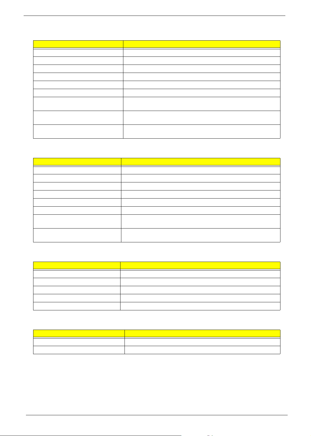
Front Panel Aspire 3300S
The computer’s front panel consists of the following:
Label Icon Color Description
1 Floppy drive light-emitting diode (LED)
2 3.5-inch floppy drive
3 Floppy drive eject button
4
CD-ROM/DVD-ROM/CD-RW Headphone/Earphone jack.
5 Volume control tuner
6
7
8 CD-ROM/DVD-ROM/CD-RW emergency eject
9
10 Black
11 Pink Microphone-in port (front)*
12 Lime Headphone-out port
CD-ROM/DVD-ROM/CD-RW LED
CD-ROM/DVD-ROM/CD-RW tray
hole
Stop/Eject button
USB ports
4 Chapter 1
Page 11
Label Icon Color Description
13 Hard disk drive activity LED
14
15
16
LAN Activity LED
Power LED
Power switch
NOTE: *The system has two microphone-in ports (front and rear). However, you cannot use both of them at
the same time. The default setting for your system enables the microphone-in port in front and disables
the one at the back.
Chapter 1 5
Page 12
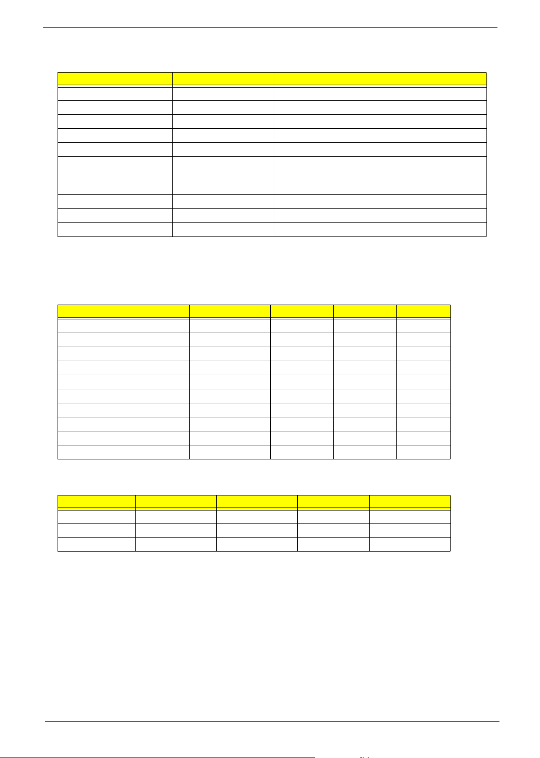
Rear Panel Aspire 3300S
Label Icon Color Description
1
2 Voltage selector switch
3
4
Green
Power supply
Keyhole
PS/2 mouse port
5
6
7
8
9
10 Power cord socket
Gray
Burgundy
Gold
Black Handset/telephone line ports (optional)
Network port
Parallel/Printer port
Game/MIDI port
VGA port
*
6 Chapter 1
Page 13
Label Icon Color Description
11 Purple PS/2 keyboard port
12 Black USB ports
13 Teal or
Turquoise
14 Lime
15 Light blue Audio-in/Line-in jack
16
17
Serial port
Audio-out/Line-out jack
Microphone-in port (rear)**
Expansion slots
NOTE: * The CRT monitor port is automatically disabled when an add-on VGA card is installed into the
system. Connect the monitor to the VGA port instead.
** The system has two microphone-in ports (front and rear). However, you can not use both of them at
the same time. The default setting for your system enables the microphone-in port in front and disables
the one at the back.
Chapter 1 7
Page 14
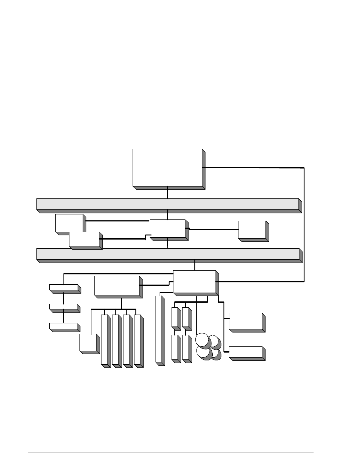
System Block Diagram (Aspire 3300S)
AGP Slot
connector
PCI Slot
PCI Slot
PCI Slot
3 X PCI Slot
1 X Parallel
2 X Serial
1 X FDD CONN
VGA
FWH
(BIOS)
4X AGP Bus
66-MHz
LPC SUPER I/O
S
P
E
A
R
R
I
A
A
L
L
L
E
A
L
INTEL P4 CPU
Willamette / Northwood
(FC-PGA2_478)
Host Bus
SIS 650
North Bridge
Primary PCI Bus
K
E
Y
B
S
E
R
F
I
D
A
D
L
B
O
A
R
D
/
M
O
U
S
E
2 IDE Ports
(Ultra DMA/ATA100)
400 MHz
33MHz,32-bit
SIS 961
South Bridge
H
H
D
D
D
D
C
C
D
R
O
M
USB
D
R
USB
O
M
133MHz
64-bit
USB
USB
4 USB Ports
X86 Legacy Signals
DDRAM
2XDIMMs
LAN
RTL8100L
AC' 97
Audio Codec
8 Chapter 1
Page 15

Chapter 1 9
Page 16
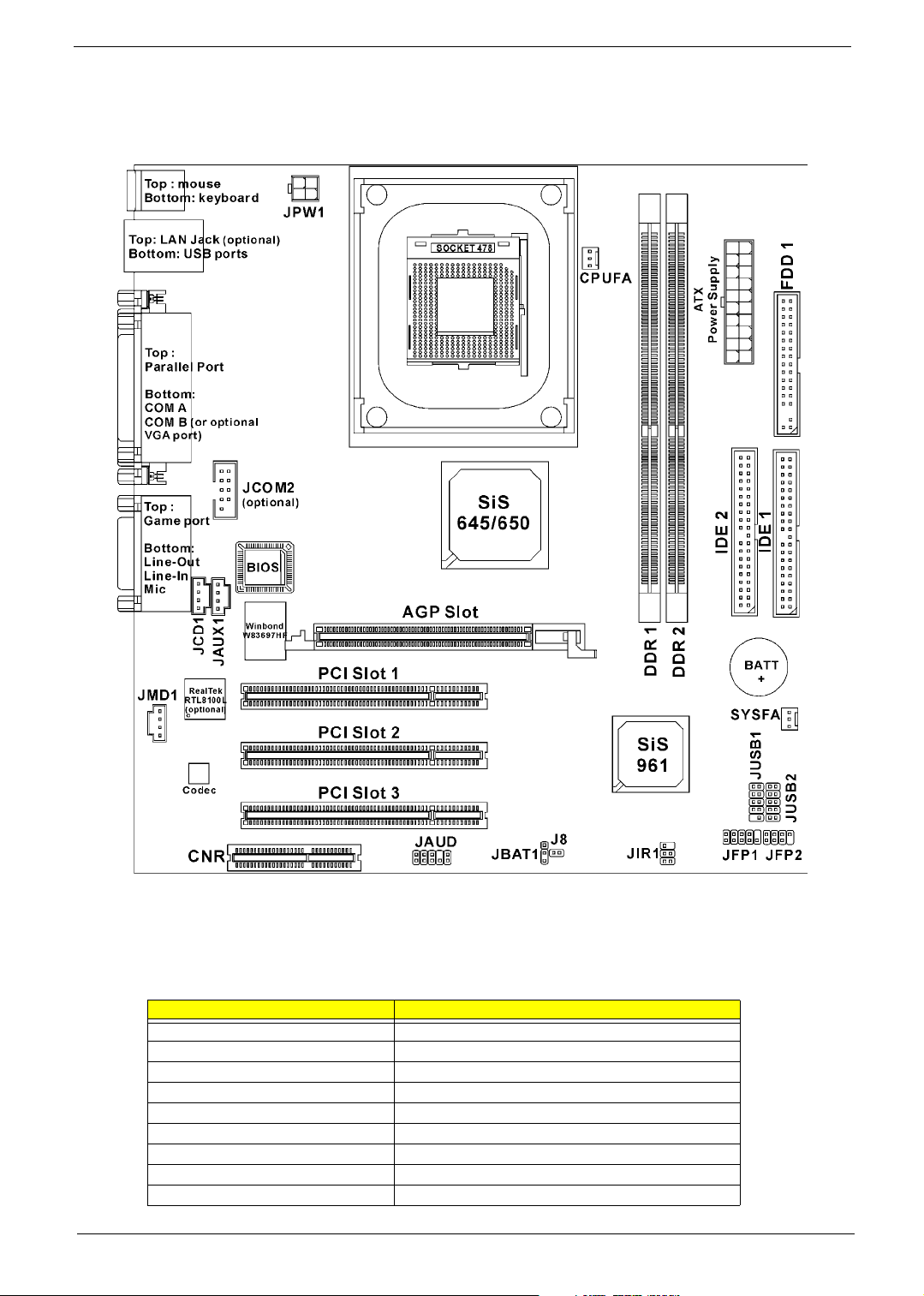
Main Board Layout (Aspire 3300S)
Component Function
ATX Power Supply/JPW1 ATX power connectors
JKBMS1 Mouse/keyboard connector
USB Connectors Connecting to USB devices
COM A & COM B Serial port connector
VGA DB 15-pin Connecting to VGA monitor
LAN Jack (optional) Connecting to LAN devices
LPT1 Parallel port connector
FDD1 Floppy disk drive connector
J8 Chassis intrusion switch connector
10 Chapter 1
Page 17

Component Function
IDE 1~IDE 2 Hard disk connector
JCD1/JAUX1/JMD1 CD/AUX/Modem-in connectors
CPUFA/SYSFA Fan power connectors
JFP1/JFP2 Front panel connectors
JAUD Front panel audio connector
JUSB1/JUSB2 USB front connector
JIR1 IrDA infrared module connector
JBAT1 Clear CMOS jumper
AGP Slot Connecting to AGP cards
PCI Slot Connecting to expansion cards
CNR Slot Connecting to expansion cards
Chapter 1 11
Page 18
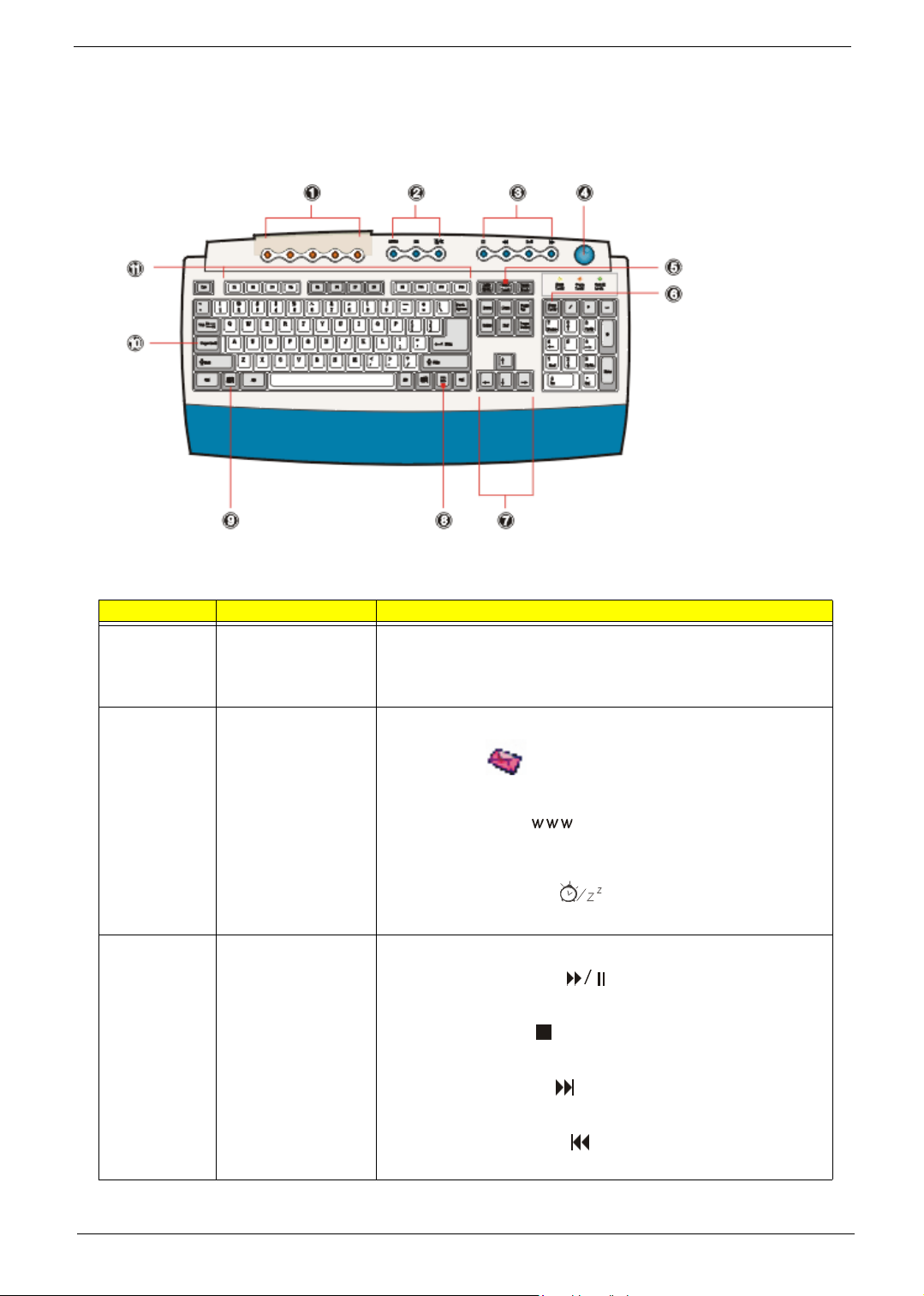
Keyboard
The keyboard has full-sized keys that include separate cursor keys, two Windows keys, and twelve function
keys.
No. Component Description
1 Programmable keys
2
3 Multimedia keys
Internet/Suspend keys Consist of three buttons:
Help you directly access a URL (Web site) or launch any program, file, or
application in your system. The fifth key is set to launch the media player.
To configure the settings of each key, right-click on the Magic Keyboard
icon located on your Windows desktop.
• Email : launches the email application that came bun-
dled with your system.
• Web browser : launches the browser application that
came bundled with your system.
• Suspend/Resume : puts the system to sleep when
pressed. To wake up the system press it again.
Allow you to do the following:
• Play/Pause button : press to start playing the audio
track or video file. Press again to pause.
• Stop Button : press to stop playing the audio track or
video file.
• Forwa rd Button : press to skip forward to the next track
or file and start playing.
• Backward button : press to skip backward to the previous track or file and start playing.
12 Chapter 1
Page 19
No. Component Description
4
Volume control/Mute
knob
Controls the speaker volume. Turn it clockwise or counterclockwise to
adjust the volume. Press it to toggle between mute and sound.
5
6
7
8
9
10
11
Scroll Lock
[
Num Lock
When activated, the screen moves one line up or down when you press
the up arrow or down arrow respectively. Take note that
with some applications.
When activated, the keypad is set to numeric mode, i.e., the keys function
as a calculator (complete with arithmetic operators such as +, -, * and /).
[may not work
]
Cursor keys
Application key
Windows logo key Start button. Combinations with this key perform special functions, such
Caps lock
@
Function keys
Also called arrow keys, let you move the cursor around the screen. They
serve the same function as the arrow keys on the numeric pad when the ]
is toggled off.
Opens the applications context menu (same function as clicking the right
button of the mouse).
as:
• Windows + Tab: Activates the next Taskbar button
• Windows + E: Explore My Computer
• Windows + F: Find Document
• Windows + M : Minimize All
• Shift + Windows + M: Undo Minimize All
• Windows + R: Displays Run dialog box
When activated, all alphabetic characters typed appear in uppercase
(same function as pressing
Access most of the computer's controls like screen brightness, volume
output and the BIOS utility.
j + <letter>).
Chapter 1 13
Page 20
Hardware Specifications and Configurations
Processor
Item Specification
Type Intel® Pentium IV processors with mPGA478 package
Slot Socket mPGA478
Speed Internal : 1.5~2.4GHz+
External: 400MHZ Data Bus Frequency
Minimum operating speed 0 MHz (If Stop CPU Clock in Sleep State the BIOS Setup is set to Enabled.)
Voltage Processor voltage can be detected by the system without setting any jumper.
BIOS
Item Specification
BIOS code programmer Award
BIOS version V6.0
BIOS ROM size 2MB
Support protocol PCI 2.1, APM1.2, DMI 2.00.1, E-IDE, ACPI 1.0, ESCD 1.03, ANSI ATA 3.0, PnP
Boot from CD-ROM feature Yes
Support to LS-120 drive No
Support to BIOS boot block feature Yes
1a, Bootable CD-ROM 1.0, ATAPI
NOTE: The BIOS can be overwritten/upgraded using the FLASH utility (AWDFLASH.EXE).
BIOS Hotkey List
Hotkey Function Description
c
Enter BIOS Setup Utility Press while the system is booting to enter BIOS
Setup Utility.
14 Chapter 1
Page 21
This section has two table lists, system memory specification and the possible combinations of memory
module.
System Memory
Item Specification
Memory socket number 2 slots (4 banks)
Support memory size per socket 64MB~1GB
Support maximum memory size 2GB
Support memory type DDR SDRAM
Support memory speed 266MHz(PC2100)
Support memory voltage 2.5V
Support memory module package 184 -pin DIMM
Support to parity check feature Yes
Support to Error Correction Code (ECC)
feature.
Memory module combinations You can install memory modules in any combination as long as they match
Yes
the Memory Combination specifications.
Memory Combinations
Slot Memory Module Tot al Memor y
Slot 1 (Bank 0 & Bank 1)64MB, 128MB,
256MB, 512MB, 1GB
Slot 2 (Bank 0 & Bank 1)64MB, 128MB,
256MB, 512MB, 1GB
64MB~1GB
64MB~1GB
Maximum System Memory Supported 64MB~2GB
Cache Memory
Item
First-Level Cache Configurations
Cache function control Enable/Disable by BIOS Setup (Advanced options)
Second-Level Cache Configurations: Below information is only applicable to system with installed Pentium 4
processor.
L2 Cache RAM size Pentium IV processor: 256 KB
L2 Cache RAM speed The same with the processor core clock frequency
L2 Cache function control Enable/Disable by BIOS Setup
Video Interface
Item Specification
Video controller resident bus AGP bus
Video interface support 1x / 2x / 4x AGP Signaling and 2x / 4x Fast Writes
The AGP buffers operate only 1.5V mode
Chapter 1 15
Page 22
Audio Interface
Item Specification
Audio controller SiS961
Audio controller resident bus AC’97 link
Audio function control Enable/disable by BIOS Setup
Mono or stereo Stereo
Resolution 16 bits
Compatibility AC’97 2.1 compliant
Sound Blaster Pro compatible
Mixed digital and analog high performance chip
Enhanced stereo full duplex operation
High performance PCI audio accelerator
Full native DOS games compatibility
High-Quality ESFM music synthesizer
MPU-401(UART mode) interface for wavetable synthesizers and MIDI devices
Integrated dual game port
Meets PC 97/PC98 and WHQL specifications
Music synthesizer Yes
Sampling rate 44.1 KHz
MPU-401 UART support Yes
Microphone jack Supported
On audio-I/O board (connects via CN6)
Headphone jack Supported On audio-I/O board (connects via CN6)
IDE Interface
Item Specification
IDE controller SiS961
IDE controller resident bus PCI bus
Number of IDE channel 2 onboard: 40-pin hard disk drive connector,
Support IDE interface E-IDE (up to PIO mode 4 and Ultra DMA/33, Ultra DMA/66 and Ultra DMA/100
mode 2) ANSIS ATA rev.4.0 ATAPI
Support bootable CD-ROM Yes
Floppy disk drive Interface
Item Specification
Floppy disk drive controller LPC Super I/O
Floppy disk drive controller resident bus LPC
Support FDD format 360KB, 720KB, 1.2MB, 1.44MB, 2.88MB; 3-mode
16 Chapter 1
Page 23
Parallel Port
Item Specification
Parallel port controller LPC Super I/O
Parallel port controller resident bus LPC
Number of parallel ports 1
Support ECP/EPP SPP/ECP / EPP 1.7 & 1.9
Connector type 25-pin D-type female connector
Parallel port function control Enable/disable by BIOS Setup
Optional ECP DMA channel
(in BIOS Setup)
Optional parallel port I/O address
(via BIOS Setup)
Optional parallel port IRQ
(via BIOS Setup)
DMA channel 1
DMA channel 3
378h
278h
IRQ5
IRQ7
Serial Port
Item Specification
Serial port controller LPC Super I/O
Serial port controller resident bus LPC
Number of serial port 2
Serial ports location COM1, COM 2
16550 UART support Yes
Connector type 10-pin connector
Optional serial port I/O address
(via BIOS Setup)
Optional serial port IRQ
(via BIOS Setup)
3F8h, 2F8h, 3E8h, 2E8h
4, 3
Modem
Item Specification
Fax modem data baud rate (bps) 14.4K bps
Data modem data baud rate (bps) 56K bps
Voice modem Yes
Modem connector type Not Applicable
Full duplex Not applicable
USB Port
Items Specifications
Universal HCI USB 1.1
USB Class Support legacy keyboard for legacy mode
Chapter 1 17
Page 24
Memory Address Map
Address Size Function
000000 - 07FFFF 512KBytes Host Memory
080000 - 09FFFF 128KBytes Host/PCI Memory
0A0000 - 0BFFFF 128KBytes PCI/ISA Video Buffer Memory
0C0000 - 0C7FFF 32KBytes Video BIOS Memory
0C8000 - 0DFFFF 96KBytes ISA Card BIOS & Buffer Memory
0E0000 - 0EFFFF 64KBytes BIOS Extension Memory
Setup and Post Memory
PCI Development BIOS
0F0000 - 0FFFFF 64KBytes System BIOS Memory
100000 - UPPER LIMIT Main Memory
UPPER LIMIT - 4GBytes PCI Memory
Note : UPPER LIMIT means the maximum size of installed memory.
The Main Memory Maximum size are 768M Bytes.
Onboard Device ID & IRQ Map
Device AD# IDSEL Route Reg. Mask
Intel 845 MCH AD11 00h
P2P AD30 13h
(Func.0) ICH2 (LPC) AD31 14h
(Func.1) ICH2 (IDE) AD31 14h
(Func.2) ICH2 (USB) AD31 14h 68h FFh
(Func.3) ICH2 (SMBUS) AD31 14h
(Func.5) ICH2 (AC97 Audio) AD31 14h 61h FFh
PCI Slot 1 AD16 05h 60h FFh
PCI Slot 2 AD17 06h 61h FFh
PCI Slot 3 AD21 07h 62h FFh
PCI Slot IRQ Routing Map
PCI INTX# INTA INTB INTC INTD
PCI 1 Route 1 Route 2 Route 3 Route 4
PCI 2 Route 2 Route 3 Route 4 Route 1
PCI 3 Route 3 Route 4 Route 1 Route 2
18 Chapter 1
Page 25
I/O Address Map
000-00F
020-021
040-043
060-060
061-061
070-071
081-08F
0A0-0A1
0C0-0DF
0F0-0FF
170-177
1F0-1F7
278-27F
2F8-2FF
378-37F
3F0-3F5
3F6-3F6
3F7-3F7
3F8-3FF
0CF8
0CFC
778-77A
Hex Range Devices
DMA Controller-1
Interrupt Controller-1
System Timer
Keyboard Controller 8742
System Speaker
CMOS RAM Address and Real Time Clock
DMA Controller-2
Interrupt Controller-2
DMA Controller-2
Math Co-Processor
Secondary IDE
Primary IDE
Parallel Printer Port 2
Serial Asynchronous Port 2
Parallel Printer Port 1
Floppy Disk Controller
Secondary IDE
Primary IDE
Serial Asynchronous Port 1
Configuration Address Register
Configuration Data Register
Parallel Printer Port 1
IRQ Assignment Map
IRQx System Devices Add-On-Card Devices
IRQ0 Timer N (Notes)
IRQ1 Keyboard N
IRQ2 Cascade Interrupt Control N
IRQ3 Serial Alternate Reserved
IRQ4 Serial Primary Reserved
IRQ5 Parallel Port (Alternate) Reserved
IRQ6 Floppy Diskette Reserved
IRQ7 Parallel Port Reserved
IRQ8 Real Time Clock N
IRQ9 N Reserved
IRQ10 N Reserved
IRQ11 N Reserved
IRQ12 PS/2 Mouse Reserved
IRQ13 Math Co-processor Exception N
IRQ14 Fix Diskette Reserved
IRQ15 Fix Diskette Reserved
NOTE: N - Not to be used.
Chapter 1 19
Page 26
DRQ Assignment Map
DRQx System Devices Add-On-Card Devices
DRQ0 N (Notes) Reserved
DRQ1 N Reserved
DRQ2 Floppy Diskette N
DRQ3 N Reserved
DRQ4 Cascade N
DRQ5 N Reserved
DRQ6 N Reserved
DRQ7 N Reserved
NOTE: N - Not to be used.
Main Board Major Chips
Item Controller
North Bridge SiS 650
South Bridge SiS 961
Super I/O controller ITE IT8705F
Audio controller SiS961
LAN controller SiS961
HDD controller SiS961
Keyboard controller SiS961
RTC SiS961
Environmental Requirements
Item Specifications
Temperature & Humidity
Operating +10 to +45°C
Non-operating -10 to +60°C
Non-operating -20 to +60°C (Storage package)
Humidity
Operating 20% to 80% RH, non-condensing
Non-operating 20% to 80% RH, non-condensing (Unpacked)
Non-operating 20% to 80% RH, non-condensing (Storage package)
Vibration
Operating
Sweep Rate
Direction
Test Cycles
Non-operating
(Packed)
Sweep rate
Direction
Test Cycles
5~16.2Hz 0.388mm(peak to peak)
16.2~250Hz 0.2G
1 octave/minute
X,Y,Z axis
2 cycles per axis
5~27.1Hz 0.6G
27.1~50Hz 0.44mm(peak to peak)
50~500Hz 2.0G
0.5 octave/minute
X,Y,Z axis
4 cycles per axis
20 Chapter 1
Page 27
Mechanical Specifications
Item Specification
Weight
One 3.5 FDD and one 3.5 HDD
(without packing)
Depends on local configuration
Switching Power Supply
Input Frequency Frequency Variation Range
50Hz 47Hz to 53Hz
60Hz 57Hz to 63Hz
Input Voltage Variation Range
100 - 120 VRMS 90-132 VRMS
200 - 240 VRMS 180-264 VRMS
Input Current Measuring Range
3A 180 - 264 VRMS
(This is for 160W power supply)
Output Requirements Regulation Current Rating(Max)
+5V +-5% 8A
+12V +-5% 8A
-12V +-10% 0.3A
+3.3 +-5% 10A
-5V +-10% 0.2A
+5V +-5% 3A
NOTE: 1. +3.3V and +5V total output power can’t exceed 80W.
Chapter 1 21
Page 28

Power Management Functions
Device Standby Mode
T Independent power management timer for hard disk drive devices
(0-15 minutes, time step=1 minute).
T Hard disk drive goes into Standby mode (for ATA standard interface).
T Disable V-sync to control the VESA DPMS monitor.
T Resume method: device activated (Keyboard for DOS, keyboard & mouse for Windows).
T Resume recovery time: 3-5 sec.
Global Standby Mode
T Global power management timer (2-120 minutes, time step=10 minute).
T Hard disk drive goes into Standby mode (for ATA standard interface).
T Disable H-sync and V-sync signals to control the VESA DPMS monitor.
T Resume recovery time: 7-10 sec.
Suspend Mode
T Independent power management timer (2-120 minutes, time step=10 minutes) or pushing external
switch button
T CPU goes into SMM.
T CPU asserts STPCLK# and goes into the Stop Grant State.
T LED on the panel turns amber color.
T Hard disk drive goes into SLEEP mode (for ATA standard interface).
T Disable H-sync and V-sync signals to control the VESA DPMS monitor.
T Return to original state by pushing external switch button.
Suspend to RAM
T The system context is maintained in system memory
T Power is shut to non-critical circuits.
T Memory is retained, and refreshes continually.
T All clocks shut except RTC.
T Return to original state by pushing external switch button & “PME” events at ACPI mode.
22 Chapter 1
Page 29

Chapter 1 23
Page 30

Chapter 2
System Utilities
Most systems are already configured by the manufacturer or the dealer. There is no need to run
Setup when starting the computer unless you get a Run Setup message.
The Setup program loads configuration values into the battery-backed nonvolatile memory called CMOS RAM.
This memory area is not part of the system RAM.
NOTE: If you repeatedly receive Run Setup messages, the battery may be bad/flat. In this case, the system
cannot retain configuration values in CMOS.
Before you run Setup, make sure that you have saved all open files. The system reboots immediately after
you exit Setup.
Chapter 2 24
Page 31

Entering Setup
Power on the computer abd the system will start POST (Power On Self Test)prosecc. When the message of
“Press DEL to enter SETUP” appears on the screen, press the key of [Delete] to enter the setup menu.
NOTE: If the message disappears before you respond and you still wish to enter Setup, restart the system by
turning it OFF and On. You may also restart the system by simultaneously pressing [Ctrl+Alt+Delete].
The Setup Utility main menu then appears:
25 Chapter 2
Page 32

The command line at the bottom of the menu tells you how to move within a screen and from one screen to
another.
T To select an option, move the highlight bar by pressing or then press .
T To change a parameter setting, press or until the desired setting is found.
T Press to return to the main menu. If you are already in the main menu, press again to
exit Setup.
The parameters on the screens show default values. These values may not be the same as those in your
system.
The grayed items on the screens have fixed settings and are not user-configurable.
NOTE: Due to the application of a new version of BIOS Setup program, you may find the BIOS menu is largely
different from the former models. However, you will soon find out that this version is much more
compact than the former ones.
Chapter 2 26
Page 33

Product Information
The screen below appears if you select Product Information from the main menu:
The Product Information menu contains general data about the system, such as the product name, serial
number, BIOS version, etc. These information is necessary for troubleshooting (maybe required when asking
for technical support).
27 Chapter 2
Page 34

The following table describes the parameters found in this menu:
Parameter Description
Product Name Displays the model name of your system.
System S/N Displays your system’s serial number.
Main Board ID Displays the main board’s identification number.
Main Board S/N Displays your main board’s serial number.
System BIOS Version Specifies the version of your BIOS utility.
SMBIOS version The System Management Interface (SM) BIOS allows you to check your system
hardware components without actually opening your system. Hardware checking
is done via software during start up. This parameter specifies the version of the
SMBIOS utility installed in your system.
System BIOS ID Specifies the version ID of the BIOS utility.
BIOS Release Date Displays the release date of the BIOS utility.
Chapter 2 28
Page 35

Standard CMOS Features
Select Standard CMOS Features from the main menu to configure some basic parameters in your system.
The following screen shows the Standard CMOS Features menu:
The following table describes the parameters found in this menu. Settings in boldface are the default and
suggested settings.
Parameter Description Options
Date Lets you set the date following the weekday-
month-day-year format
Time Lets you set the time following the hour-minute-
second format
IDE Primary Channel Master Allows you to configure the hard disk drive
connected to the master port of IDE channel 1.
To enter the IDE Primary Master setup, press
[Enter].
The IDE CD-ROM is always automatically
detected.
IDE Primary Channel Slave Allows you to configure the hard disk drive
connected to the slave port of IDE channel 1.
To enter the IDE Primary Slave setup, press
[Enter].
The IDE CD-ROM is always automatically
detected.
Weekday: Sun, Mon...Sat
Month: Jan, Feb...Dec.
Day: 1 to 30
Year: 1980 to 2079
Hour: 0 to 23
Minute: 0 to 59
Second: 0 to 59
IDE Device Model Number:
None
IDE Device Model Number:
None
29 Chapter 2
Page 36

Parameter Description Options
IDE Secondary Channel Master Allows you to configure the hard disk drive
connected to the master port of IDE channel 2.
To enter the IDE Secondary Master setup, press
[Enter].
The IDE CD-ROM is always automatically
detected.
IDE Secondary Channel Slave Allows you to configure the hard disk drive
connected to the slave port of IDE channel 2.
To enter the IDE Secondary Slave setup, press
[Enter].
The IDE CD-ROM is always automatically
detected.
Drive A Allows you to configure your floppy drive A. 1.44 MB, 3.5-inch
Drive B Allows you to configure your floppy drive B. 1.44 MB, 3.5-inch
Floppy 3 Mode Support Floppy 3 is the standard Japanese floppy drive
mode. Supported by the BIOS, the selected
diskette drive can read 720KB, 1.2MB and
1.44MB on a 3.5” diskette.
Video This item specifies the type of video card in use.
The default setting is VGA/EGA. Since current
PCs use VGA only, this function is almost
useless and may be disregarded in the future.
Halt On This parameter enables you to control the
system stops in case of Power On Self Test
errors (POST).
Base Memory Refers to the option of memory that is available
to standard DOS programs. DOS systems have
an address space od 1MB, but the top 384KB
(called high memory) is reserved for system use.
This leaves 640 KB of conventional memory.
Everything above 1MB is either extended or
extended memory.
Extended Memory Memory above and beyond the standard 1MB of
base memory that DOS supports. Extended
memory is only available in PCs with an Intel
80286 or later microprocessor. Extended
memory is not configured in any special manner
and is therefore unavailable to most DOS
programs. However, MS Windows and OS/2
can use extended memory.
Total Memory Total based and extended memory, and I/O
ROM 384KB available to the system.
IDE Device Model Number:
None
IDE Device Model Number:
None
None
360 KB, 5.25-inch
1.2 MB, 5.25-inch
720 KB, 3.5-inch
2.88 MB, 3.5-inch
None
360 KB, 5.25-inch
1.2 MB, 5.25-inch
720 KB, 3.5-inch
2.88 MB, 3.5-inch
Disabled, Enabled.
VGA/EGA
CGA40
CGA80
Mono
All Errors
No Errors
All but Keyboard
All but Diskette
All by Disk/Key
Chapter 2 30
Page 37

IDE Primary/Secondary Channel Master/Slave Setup
The following screen appears if you select any of the IDE drive parameters:
The following table describes the parameters found in this menu. Settings in boldface are the default and
suggested settings.
Parameter Description Options
IDE HDD AutoDetection
IDE Primary Master Display the type of device installed. Auto
Access Mode Selects the HDD access mode Auto
Capacity Shows the size of your HDD in MB xxxxx MB
Cylinder Shows your hard disk’s numberof cylinders 0 to 65535
Head Shows your hard disk’s number of heads 0 to 255
Precomp Selects the precomp number for old HDD parking 0 to 65535
Landing Zone Selects the Land Zone number for old HDD parking 0 to 65535
Sector Shows your hard disk’s number of sectors 0 to 255
Auto-detects your hard disk drive Press [Enter]
None
Manual
Large
LBA
CHS
31 Chapter 2
Page 38

Advanced BIOS Features
The following screen shows the Advanced BIOS Features:
The following table describes the parameters found in this menu. Settings in boldface are the default and
suggested settings.
Parameter Description Options
Virus Warning Allows you to set the virus warning feature for
IDE Hard Disk boot sector protection. If the
function is enabled and any attempt to write
data into this area is made, BIOS will display a
warning message on screen and beep.
Quick Power On Self Test This parameter speeds up POST by skipping
some items that are normally checked.
Hard Disk Boot Priority
First/Second/Third Boot
Device
Boot Other Device This parameter allows you to specify the system
Swap Floppy Drive Setting to Enabled will swap floppy drive a: and
Boot Up Floppy Seek Setting to Enabled will make BIOS seek floppy
The items allow you to set the sequence of boot
device where BIOS attempts to load the disk
operating system.
boot up search sequence.
b:.
drive a: before booting the system.
Enabled
Disabled
Enabled
Disbaled
Floppy, LS120, HDD-0, SCSI,
CDROM, HDD-1, HDD-2, HDD-3, ZIP,
LAN, Disabled (Disable this sequence
).
The sequence following the order of
HDD, Floppy and CD-ROM is
recommended.
Enabled
Disbaled
Enabled
Disabled
Enabled
Disabled
Chapter 2 32
Page 39

Parameter Description Options
Boot Up NumLock Status Sets the NumLock status when the system is
powered on. Setting to On will turn on the
NumLock key when the system is powered on.
Setting to Off will allows users to use the arrow
keys on the numeric keypad.
Gate A20 Option This item is to set the Gate A20 status. A20
refers to the first 64KB of extended memory.
When the default value Fast is selected, the
Gate A20 is controlled by port 92 or chipset
specific method resulting in faster system
performance. When Normal is selected, A20 is
controlled by a keyboard controller or chipset
hardware.
Typematic Rate Setting This item is used to enable or disable the
typematic rate setting including Typematic Rate
and Typematic Deplay.
On
Off
Fast
Normal
Enabled
Disabled
Typematic Rate After Typematic Rate Setting is enabled, this
item allows you to set the rate (characters/
second) at which at keys are accelerated.
Typematic Delay This item allows you to select the delay
between when the key was first pressed and
when the acceleration begins
Security Option Specifies the type of BIOS password protection
that is implemented. Setup means that the
password prompt appears only when end users
try to run Setup. System means that a
password prompt appears every time when the
computer is powered on or when end users try
to run Setup.
APIC Mode This field is used to enable or disable the APIC
(Advanced Programmable Interrupt Controller).
Due to compliance with PC2001 design guide,
the system is able to run in APIC mode.
Enabling APIC mode will expand available IRQ
resources from the system.
MPS Version Control for OS This field allows you to select which MPS (Multi-
Processor Specification) version to be used for
the operating system. You need to select the
MPS version supported by your operating
system. To find out which version to use,
consult the vendor of your operating system.
Settings: 6,8,10,12,15,20,24 and 30.
Settings: 250, 500, 750 and 1000.
Setup
System
Enabled
Disabled
1.4
1.1
33 Chapter 2
Page 40

Advanced Chipset Features
The advanced cipset features setup option is used to change the values of the chipset registers. These
registers control most of the system options in the computer.
NOTE: Change these settings only if you are familiar with the chipset.
Advanced DRAM Control
Press [Enter] to enter the sub-menu and the following screen appears:
Chapter 2 34
Page 41

The following table describes each parameter under the sub-menu. Settings in boldface are the default and
suggested values.
Parameter Description Options
System Performance The DRAM timing is controlled by the DRAM
Timing Registers. The timings programmed into
this register are dependent on the system
design. Slower rates may be required in certain
system designs to support loose layouts or
slower memory.
CAS Latency Setting When synchronous DRAM is installed, the
number of clock cycles of CAS latency depends
on the DRAM timing.
Normal Mode
Safe Mode
Fast mode
Turbo Mode
Ultra Mode
2T, 2.5T, 3T
The other two parameters under the Advanced Chipset Features are presented below. Settings in boldface
are the deafult and suggested values.
Parameter Description Options
Memory Hole at 15M-16M You can reserve this area of system memory for
ISA adapter ROM. When this area is reserved, it
cannot be cached. The user information of
peripherals that need to use this area of system
memory usually discuss their memory
requirements.
AGP Aperture Size (MB) This item lets you determine the effective size of
the AGP Graphic Aperture.
Disabled
Enabled
64, 4,8,16,32,128 and 256.
35 Chapter 2
Page 42

Integrated Peripherals
The following table describes each Integrated Peripherals parameters. Settings in boldface are the default
and suggested values.
Parameter Description Options
Internal PCI/IDE This setting enables or disables the internal
primary and secondary PCI & IDE controllers.
IDE Primary Master PIO
IDE Primary Slave PIO
IDE Secondary Master PIO
IDE Secondary Slave PIO
Primary Master UltraDMA
Primary Salve UltraDMA
Secondary Master UltraDMA
Secondary Slave UltraDMA
IDE Burst Mode This allows your hard disk controller to use the
AC97 Audio Enabling the on-die AC97 Auto if no add-on PCI
System Share Memory Size For SiS650 chipset, the system shares memory
USB Controller This item is used to enable or disable the on-chip
Setting these items to “Auto” activates the HDD
speed auto-detect function. The PIO mode
specifies the data transfer rate of the HDD. For
example, mode 0 data transfer rate is 3.3MB/s,
mode 1 is 5.2 MB/s, mode 2 is 8.3MB/s, mode 3
is 11.1 MB/s and mode 4 is 16.6MB/s. If your
hard disk performance becomes unstable, you
may manually try the slower mode.
These items allow you to set the Ultra DMA 33/
66/100 mode supported by the hard disk drive
connected to your primary and secondary IDE
connectors.
fast block mode to transfer data to and from the
hard disk drive.
audio device.
to the onboard VGA card. This setting controls
the exact memory size shared to the VGA card.
USB.
Both, Disabled, Primary,
Secondary
Auto, mode 1, mode 2, mode 3
and mode 4
Auto
Disables
Enabled
Disabled
Auto
Disabled
4, 8, 16, 32, 64MB
Enabled
Disabled
Chapter 2 36
Page 43

Parameter Description Options
USB Keyboard Support This item lets you enable or disable the USB
keyboard driver within the onboard BIOS. The
keyboard driver simulates legacy keyboard
command and lets you use a USB keyboard
during POST or after boot if you do not have a
USB driver in the operating system.
USB Mouse Support This item lets you enable or disable the USB
mouse driver within the onboard BIOS. The
keyboard driver simulates legacy mouse
command and lets you use a USB mouse during
POST or after boot if you do not have a USB
driver in the operating system.
Onboard LAN function To enable or disable the onboard LAN controller Enabled
Onboard LAN Boot ROM This setting determines whether or not to
activate the boot ROM of the onboard LAN chip.
IDE HDD Block Mode Block mode is also called block transfer, multiple
commpands or multiple sector read/write. If your
IDE hard drive supports block mode (most new
drives do), select “Enabled” for automatic
detection of the optimal number of block read/
write per sector the drive can support.
Onboard FDC Controller Setting this parameter to “Enable” allows you to
connect your floppy disk drives to the onboard
floppy disk connector instead of a separate
controller card. Change the setting to “Disabled”
if you want to use a separate controller card.
Enabled
Disabled
Enabled
Disabled
Disabled
Enabled
Disabled
Enabled
Disabled
Enabled
Disabled
37 Chapter 2
Page 44

Power Management Setup
The Power Management menu lets you configure your system to most effectively save energy while operating
in a manner consistent with your own style of computer use.
The following screen shows the Power Management parameters and their default settings:
The following table describes the parameters found in this menu. Settings in boldface are the default and
suggested settings.
Parameter Description Options
ACPI Function This item is to activate the ACPI (Advanced
Configuration and Power Management Interface)
Function. If your operating system is ACPIaware, such as Windows 98SE/2000/Me, select
Enabled.
ACPI Suspend Type This item specifies the power saving modes for
ACPI function. S1(POS): The S1 sleep mode is
a low power state. In this state, no system
context (CPU or chipset) is lost and hardware
maintains all system context. S3 (STR): The S3
sleep mode is s power-down state in which
power is supplied only to essential components
such as main memory and wake-capable
devices and all system context is saved to main
memory. The information stored in memory will
be used to restore the PC to the previous state
when an wake-up event occurs. S1&S3: Both S1
and S3 will be adopted.
Enabled
Disabled
S3
S1
S1&S3
Chapter 2 38
Page 45

Parameter Description Options
Video Off Option This item is to control the mode in which the
monitor will shut down.
Always On: Always keep the monitor on.
Suspend --> Off: During suspend mode, the
monitorwill shut down. Susp, Stby --> During
suspend or standby mode, the monitor will shut
down. All Modes --> Off: The monitor is turned
off during doze, standby or suspend mode.
Video Off Method This item determines the manner in which the
monitor is blanked.
V/H SYNC+Blank: This selection will cause the
system to turn off the vertical and horizontal
synchronization ports and write blanks to the
video buffer. Blank Screen: This option only
write blanks to the video buffer. DPMS
Supported: Initial display power management
signaling.
Modem Use IRQ This setting names the interrupt request (IRQ)
line assigned to the modem (if any) on your
system. Activity of selected IRQ always
awakens the system.
HDD Power Down If HDD activity is not detected for the length of
time specified in this field, the hard disk drive will
be powered down while all other devices remain
active.
Soft-off by PWR-BTTN This feature allows users to configure the power
button function.
Aftrer PC Power Lost This item specifies when your system reboot
after a power failure or interrupt occurs.
Power On by Ring When enabled, any fax/modem activity wakes up
the system from suspend mode.
Wake-Up by PCI Card Use PCI Wake-up system. PCI must meet PCI
2.2 specification.
Resume by Alarm Use this option to set the date and time for your
computer to boot up.
Date (of month) Alarm* - Indicate the month for
system to boot up. Set it to 0 if you want to boot
up everyday.
Time (hh:mm:ss) Alarm* - Indicate the hour,
minute and second for system to boot up.
Always On
Suspend Off
Susp, Stby --> Off
All Modes
V/H SYNC+Blank
Blank Screen
DPMS Supported
3, 4, 5, 7, 9, 10, 11, AUTO.
Disabled
1~15 Mins
Instant Off: The power button
functions as a normal poweron/-off button.
Delay 4 Sec: When you press
the power button, the
computer enters the suspend/
sleep mode, but if the button is
pressed for more than four
seconds, the computer will be
turned off.
Power Off
Power On
Last State
Disabled
Enabled
Disabled
Enabled
Disabled
Enabled
*Set Resume by Alarm to
Enable, then press “Enter” to
show the range of Date and
Time Alarm.
39 Chapter 2
Page 46

PnP/PCI Configuration
The following table describes the parameters found in this menu. Settings in boldface are the default and
suggested settings.
Parameter Description Options
Reset Configuration Data Selecting “Enabled” to reset Extended System
Configuration Data (ESCD) only if you installed
a new add-on and the system reconfiguration
has caused such a serious conflict that the
operating system can not boot. Otherwise, you
should leave it unchanged.
Resources Controlled By This BIOS can automatically configure all of the
boot and Plug and Play compatible devices.
You can also set it as Manual and go into each
of the sub menu to choose specific resources.
IRQ Resources The items are adjustable only when “Resources
Controlled By” is set to Manual. By pressing
“Enter” to access the sub menu.
PCI/VGA Palette Snoop Disabled - Data read or written by the CPU is
only directed to the PCI VGA device’s palette
registers.
Enabled - Data read or written by the CPU is
directed to both the PCI VGA device’s palette
registers and the ISA VGA device’s palette
registers, permitting the palette registers of both
VGA devices to be identical.
Disabled
Enabled
Auto (ESCD)
Manual
PCI Device
Reserved
Disabled
Enabled
*If any ISA bus adapter in the
system requires VGA Palette
snooping, the setting must be set
to “Enabled”.
NOTE: It is strongly recommended that only experienced users should make any changes to the default
settings.
Chapter 2 40
Page 47

PC Health Status
The following table describes the parameters found in this menu:
Parameter Description Options
Shutdown Temperature This option is for setting the shutdown temperature
level for the processor. When the processor
reaches the temperature you set, the ACPI-aware
system will be shut down.
Current System/CPU
Temperature, CPU/
System fan, Vcore, ect.
These items display the current status of all of the
mainboard hardware devices/components such as
CPU voltages, temperatures and all fans’ speeds.
41 Chapter 2
Page 48

Frequency Control
The following table describes the parameters found in this menu. Settings in boldface are the default and
suggested settings.
Parameter Description Options
Set CPU Ratio End users can overlock the processor by
specifying the CPU ratio (clock multiplier) in this
field.
CPU Clock Ratio If the CPU Ratio is set to Manual, end users can
choose a suitable ratioto support the CPU.
Auto Detect DIMM/PCI Clk This option allows you to enable/disable the
feature of auto detecting the clock frequency of
the installed DIMM/PCI bus.
Spread Spectrum When the motherboard’s clock generator pulses,
the extreme values (spikes) of the pulses creates
EMI (Electromagnetic Interference). The spread
Spectrum function reduces the EMI generated by
modulating the pulses so that the spikes of the
pulses are reduced to flatter curves. If you do
not have any EMI problem, leave the setting at
Disabled for optimal system stability and
performance. But if you are plagued by EMI,
setting to Enabled for EMI reduction. Remember
to disable Spread Spectrum if you are
overlocking because even a slight jitter can
introduce a temporary boost in clockspeed which
may just cause your overlock ed processor to
lock up.
DRAM Frequency This setting let end users select the DRAM
frequency.
Auto
Manual
8x to 50x
Enabled
Disabled
By SPD
200 Mhz
266 Mhz
333 Mhz
Chapter 2 42
Page 49

Load Default Settings
The default settings are the default values set by the mainboard manufacturer specifically for optimal
performance of the mainboard. When you select the item, a message as below appears:
Pressing Y (Yes) loads the BIOS default values for the most stable system performance.
43 Chapter 2
Page 50

Set Supervisor/User Password
When you choose to set supervisor password, a message as below will appear on the screen:
At the prompt, type your password. Your password can be up to six characters in length. After typing the
password, press “Enter”. At the next prompt, re-type your password and press “Enter” again to confirm the
new password. After the password entry, the screen automatically reverts to the main screen.
To disable the password, press “Enter” when prompted to enter the password. The following screen will
display a message confirming that the password has been disabled.
Chapter 2 44
Page 51

If you select Set User Password, a message as below will appear:
At the prompt, type your password. Your password can be up to six characters in length. After typing the
password, press “Enter”. At the next prompt, re-type your password and press “Enter” again to confirm the
new password. After the password entry, the screen automatically reverts to the main screen.
To disable User Password, press “Enter” when prompted to enter the password. The following screen will
display a message confirming that the password has been disabled.
45 Chapter 2
Page 52

Save & Exit Setup/Exit Without Saving
If you select Save and Exit Setup, you will exit the BIOS utility. The following dialogue box will appear.
Select Y (Yes) to exit Setup. Select N (No) to return to the main menu.
If you select Exit Without Saving, you will discard all the changes you made and exit Setup.
Chapter 2 46
Page 53

47 Chapter 2
Page 54

Machine Disassembly and Replacement
This chapter contains step-by-step procedures on how to disassemble the Veriton 3300/3300D desktop
computer for maintenance and troubleshooting.
To disassemble the computer, you need the following tools:
T Wrist grounding strap and conductive mat for preventing electrostatic discharge
T Flat-bladed screwdriver
T Phillips screwdriver
T Hexagonal screwdriver
T Plastic stick
NOTE: The screws for the different components vary in size. During the disassembly process, group the
screws with the corresponding components to avoid mismatches when putting back the components.
Chapter 3
Chapter 3 48
Page 55

General Information
Before You Begin
Before proceeding with the disassembly procedure, make sure that you do the following:
1. Turn off the power to the system and all peripherals.
2. Unplug the AC adapter and all power and signal cables from the system.
49 Chapter 3
Page 56

Disassembly Procedure Flowchart
The flowchart on the succeeding page gives you a graphical representation on the entire disassembly
sequence and instructs you on the components that need to be removed during servicing.
Main Unit
Upper Case
Upper Case
W/ Front Panel
Front Panel
Rotate Bracket
W/DVD-ROM &
FDD Module
DVD-ROM
Alarm Cable
USB/Audio
Intrusion
Board
EMI Audio
Cover
FDD
Audio Cable USB Cable
Power Supply HDD Module Main Board
USB/Audio
Board
Module
AGP VGA
Card
HDD HDD Bracket
DIMM
Modem Card
CPU Fan Sink
CPU
RTC Battery
Chapter 3 50
Page 57

Opening the Housing
This section tells you how to open the housing cover when you need to install additional components inside
the system unit.
CAUTION: Before you proceed, make sure that you have turned off the system and all peripherals connected
to it.
Removing the Housing Cover
1. Place the system unit on a flat, steady surface.
2. Turn the housing back.
3. Slide the upper case back out about an inch and then gently pull it outward to detach it from the housing.
51 Chapter 3
Page 58

Removing the Front Panel
1. See “Opening the Housing” on page 51
2. Remove the four screws as shown here.
3. Detach the front bezel from the front panel gently in the way as shown here.
Removing the EMI Audio Cover
1. See “Opening the Housing” on page 51
2. Remove the EMI audio cover from the lower case.
Chapter 3 52
Page 59

Removing the Modem Card
1. See “Opening the Housing” on page 51
2. Remove the screw as shown below and then remove the modem card from the slot.
Removing the AGP VGA Card
1. See “Opening the Housing” on page 51
2. Remove the screw as shown here and then remove the AGP VGA card from the slot.
Removing the FDD and DVD Frame
1. See “Opening the Housing” on page 51
2. Push the two latches of both sides then lift up the FDD and DVD frame.
53 Chapter 3
Page 60

3. Disconnect the floppy disk drive and power cables from the floppy disk drive.
4. Disconnect the power cable, IDE cable, and audio cable from the DVD-ROM drive.
5. Disconnect the micro switch cable from the main board.
6. Pull the FDD and DVD frame from the lower case.
7. Remove the four screws as shown here then detach the DVD-ROM drive from the frame.
Chapter 3 54
Page 61

8. Remove the four screws as shown here then detach the floppy disk drive from the frame.
9. Disconnect micro switch cable from the FDD and DVD frame.
Removing the Intrusion Alarm Cable
1. See “Opening the Housing” on page 51
2. See “Removing the FDD and DVD Frame” on page 53”
3. Detach the intrusion alarm cable from the FDD and DVD Frame.
55 Chapter 3
Page 62

Removing the USB and Audio Board
1. See “Opening the Housing” on page 51
2. See “Removing the EMI Audio Cover” on page 52
3. See “Removing the FDD and DVD Frame” on page 53
4. Disconnect the USB board cable and audio board cable from the USB and audio board.
5. Remove the two screws as shown here then detach the USB and audio board from the lower case.
Removing the Hard Disk Drive
1. See “Opening the Housing” on page 51
2. See “Removing the FDD and DVD Frame” on page 53
3. Disconnect the IDE cable and HDD power cable from the hard disk drive.
4. Remove the two screws as shown here and then hold the hard disk drive frame.
Chapter 3 56
Page 63

5. Slide the hard disk drive frame to the right and then gently move it inward to detach it from
the lower case.
6. Remove the four screws as shown and then detach the hard disk drive from the frame.
Removing the DIMM
1. See “Opening the Housing” on page 51
2. See “Removing the FDD and DVD Frame” on page 53”
3. To release the system memory, press down and out on the levers on both sides of the DIMM socket.
4. Gently pull the DIMM out of the socket.
57 Chapter 3
Page 64

Removing the Power Supply
1. See “Opening the Housing” on page 51.
2. See “Removing the FDD and DVD Frame” on page 53”
3. Remove the two screws as shown here.
4. Disconnect the power cable from the main board.
5. Gently remove the power supply from the system.
Removing the RTC Battery
1. See “Opening the Housing” on page 51
2. To remove the RTC battery from the holder, gently remove it from the holder by hand.
Chapter 3 58
Page 65

Removing the Processor
1. See “Opening the Housing” on page 51
2. See “Removing the FDD and DVD Frame” on page 53”
3. Disconnect the fan sink cable from the main board, and then release the two levers on both sides of the
fan sink.
.
4. Put the two levers back to the original position, and then remove the CPU fan sink from the main board
5. Lift up the socket lever, pull the CPU out from the socket carefully and then put the socket lever back to its
original position.
59 Chapter 3
Page 66

Removing the Main board
1. See “Opening the Housing” on page 51
2. See “Removing the FDD and DVD Frame” on page 53
3. Remove the six screws as shown here then detach the main board from the lower case.
Chapter 3 60
Page 67

61 Chapter 3
Page 68

Troubleshooting
This chapter provides troubleshooting information for the Aspire 3300S:
T Power-On Self-Test (POST)
T Index of Error Message
T Index of Error Symptoms
T Undetermined Problems
Chapter 4
Chapter 4 62
Page 69

Power-On Self-Test (POST)
Each time you turn on the system, the Power-on Self Test (POST) is initiated. Several items are tested during
POST, but is for the most part transparent to the user.
The Power-On Self Test (POST) is a BIOS procedure that boots the system, initializes and diagnoses the
system components, and controls the operation of the power-on password option. If POST discovers errors in
system operations at power-on, it displays error messages on screen, generates a check point code at port
80h or even halts the system if the error is fatal.
The main components on the main board that must be diagnosed and/or initialized by POST to ensure system
functionality are as follows:
T Microprocessor with built-in numeric co-processor and cache memory subsystem
T Direct Memory Access (DMA) controller (8237 module)
T Interrupt system (8259 module) or APIC (advance program interrupt controller)
T Three programmable timers (system timer and 8254 module)
T ROM subsystem
T RAM subsystem
T CMOS RAM subsystem and real time clock/calendar with battery backup
T Onboard serial interface controller
T Onboard parallel interface controller
T Embedded hard disk interface and one diskette drive interface
T Keyboard and auxiliary device controllers
T I/O ports
T Two RS232 serial ports
T One parallel port
T One PS/2-compatible mouse port
T OnePS/2-compatible keyboard port
NOTE: When Post executes a task, it uses a series of preset numbers called check points to be latched at
port 80h, indicating the stages it is currently running. This latch can be read and shown on a debug board.
The following table describes the BIOS common tasks carried out by POST. Each task is denoted by an
unique check point number. For other unique check point numbers that are not listed in the table, refer to the
correspoing product service guide.
Post Checkpoints List: The list may vary accordingly depending on your BIOS.
Checkpoint Description
CFh Test CMOS R/W functionality
C0h Early chipset initialization:
-Disable shadow RAM
-Disable L2 cache (socket 7 or below)
-Program basic chipset registers
C1h Detect memory
-Auto-detection of DRAM size, type and ECC.
-Auto-detection of L2 cache (socket 7 or below)
C3h Expand compressed BIOS code to DRAM
C5h Call chipset hook to copy BIOS back to E000 & F000 shadow RAM.
0h1 Expand the Xgroup codes locating in physical address 1000:0
02h Reserved
63 Chapter 4
Page 70

Checkpoint Description
03h Initial Superio_Early _Init switch
04h Reserved
05h 1. Blank out screen
2. Clear CMOS error flag
06h Reserved
07h 1. Clear 8042 interface
2. Initialize 8042 self-test
08h 1. Test special keyboard controller for Winbond 977 series Super I/O chips.
2. Enable keyboard interface.
09h Reserved
0Ah 1. Disable PS/2 mouse interface (optional)
2. Auto detect ports for keyboard & mouse followed by a port & interface swap (optional).
3. Reset keyboard for Winbond 977 series Super I/Q chips.
0Bh Reserved
0Ch Reserved
0Dh Reserved
0Eh Test F000h segment shadow to see whether it is R/W-able or not. If test fails, keep
beeping the speaker.
0Fh Reserved
10h Auto detect flash type to load appropriate flash R/W codes into the run time area in F000
for ESCD & DMI support.
11h Reserved
12h Use walking 1’s algorithm to check out interface in CMOS circuitry. Also set real-time clock
power status, and then check for override.
13h Reserved
14h Program chipset default values into chipset. Chipset default values are MODBINable by
15h Reserved
16h Initial Early_Init_Onboard_Generator switch.
17h Reserved
18h Detect CPU information including brand, SMI type (Cyrix or Intel) and CPU level (586 or
19h Reserved
1Ah Reserved
1Bh Initial interrupts vector table. If no special specified, all H/W interrupts are directed to
1Ch Reserved
1Dh Initial Early_PM_INIT switch.
1Eh Reserved
1Fh Load keyboard matrix (notebook platform)
20h Reserved
21h HPM initialization (notebook platform)
22h Reserved
OEM customers.
686)
SPURIOUS_INT_HDLR & S/W interrupts to SPURIOUS_soft_HDLR.
Chapter 4 64
Page 71

Checkpoint Description
23h 1. Check validity of RTC value:
e.g. a value of 5Ah is an invalid value for RTC minute.
2. Load CMOS settings into BIOS stack. If CMOS checksum fails, use default value
instead.
3. Prepare BIOS resource map for PCI & PnP use. If ESCD is valid, take into
consideration of the ESCD’s legacy information.
4. Onboard clock generator initialization. Disable respective clock resource to empty PCI
& DIMM slots.
5. Early PCI initialization
-Enumerate PCI bus number
-Assign memory & I/O resource
-Search for a valid VGA device and VGA BIOS, and put it into C000:0
24h Reserved
25h Reserved
26h Reserved
27h Initialize INT 09 buffer
28h Reserved
29h 1. Program CPU internal MTRR (P6 & PII) for 0-640K memory address.
2. Initialize the APIC for Pentium class CPU.
3. Program early chipset according to CMOS setup. Example: onboard IDE controller.
4. Measure CPU speed.
5. Invoke video BIOS.
2Ah Reserved
2Bh Reserved
2Ch Reserved
2Dh 1. Initialize multi-language
2. Put information on screen display, including Award title, CPU type, CPU speed...
2Eh Reserved
2Fh Reserved
30h Reserved
31h Reserved
32h Reserved
33h Reset keyboard except Winbond 977 series Super I/O chips.
34h Reserved
35h Reserved
36h Reserved
37h Reserved
38h Reserved
39h Reserved
3Ah Reserved
3Bh Reserved
3Ch Test 8254.
3Dh Reserved
3Eh Test 8259 interrupt mask bits for channel 1
3Fh Reserved
40h Test 8259 interrupt mask bits for channel 2.
41h Reserved
42h Reserved
65 Chapter 4
Page 72

Checkpoint Description
43h Test 8259 functionality
44h Reserved
45h Reserved
46h Reserved
47h Initialize EISA slot
48h Reserved
49h 1. Calculate total memory by testing the last double word of each 64K page.
2. Program writes allocation for AMD K5 CPU.
4Ah Reserved
4Bh Reserved
4Ch Reserved
4Dh Reserved
4Eh 1. Program MTRR of M1 CPU.
2. Initialize L2 cache for P6 class CPU & program CPU with proper cacheable range.
3. Initialize the APIC for P6 class CPU.
4. On MP platform, adjust the cacheable range to smaller one in case the cacheable
ranges between each CPU are not identical.
4Fh Reserved
50h Initialize USB
51h Reserved
52h Test all memory (clear all extended memory to 0)
53h Reserved
54h Reserved
55h Display number of processors (multi-processor platform)
56h Reserved
57h 1. Display PnP logo
2. Early ISA PnP initialization
-Assign CSN to every ISA PnP device.
58h Reserved
59h Initialize the combined Trend Anti-Virus code.
5Ah Reserved
5Bh (Optional Feature)
Show message for entering AWDFLASH.EXE from FDD (optional)
5Ch Reserved
5Dh 1. Initialize Init_Onboard_Super_IO switch.
2. Initialize Init_Onboard_AUDIO switch.
5Eh Reserved
5Fh Reserved
60h Okay to enter Setup utility; i.e. not until this POST stage can users enter the CMOS setup
61h Reserved
62h Reserved
63h Reserved
64h Reserved
65h Initialize PS/2 Mouse
66h Reserved
utility.
Chapter 4 66
Page 73

Checkpoint Description
67h Prepare memory size information for function call:
INT 15h ax=E820h
68h Reserved
69h Turn on L2 cache
6Ah Reserved
6Bh Program chipset registers according to items described in Setup& Auto-configuration
table.
6Ch Reserved
6Dh 1. Assign resources to all ISA PnP devices.
2. Auto assign ports to onboard COM ports if the corresponding item in Setup is set to
“AUTO”
6Eh Reserved
6Fh 1. Initialize floppy controller
2. Set up floppy related fields in 40: hardware.
70h Reserved
71h Reserved
72h Reserved
73h (Optional Feature)
Enter AWDFLASH.EXE if:
-AWDFLASH is found in floppy drive
-ALT+F2 is pressed
74h Reserved
75h Detect & install all IDE devices: HDD, LS120, ZIP,CDROM.....
76h Reserved
77h Detect serial ports & parallel ports
78h Reserved
79h Reserved
7Ah Detect & install co-processor
7Bh Reserved
7Ch Reserved
7Dh Reserved
7Eh Reserved
7Fh 1. Switch back to text mode if full screen logo is supported.
-If errors occur, report errors & wait for keys
-If no errors occur or F1 key is pressed to continue:
Clear EPA or customization logo.
80h Reserved
81h Reserved
82h 1. Call chipset power management hook.
2. Recover the text fond used by EPA logo (not for full screen logo)
3. If password is set, ask for password.
83h Save all data in stack back to CMOS.
84h Initialize ISA PnP boot devices.
67 Chapter 4
Page 74

Checkpoint Description
85h 1. USB final Initialization
2. NET PC: Build SYSID structure
3. Switch screen back to text mode.
4. Set up ACPI table at top of memory.
5. Invoke ISA adapter ROMs.
6. Assign IRQs to PCI devices
7. Initialize APM
8. Clear noise of IRQs/
86h Reserved
87h Reserved
88h Reserved
89h Reserved
90h Reserved
91h Reserved
92h Reserved
93h Read HDD boot sector information for Trend Anti-Virus code
94h 1. Enable L2 cache
2. Program boot up speed
3. Chipset final initialization
4. Power management final initialization
5. Clear screen & display summary table
6. Program K6 write allocation
7 Program P6 class write combining .
95h 1. Program daylight saving
2. Update keyboard LED & typematic rate
96h 1. Build MP table
2. Build & update ESCD
3. Set CMOS century to 20h or 19h
4. Load CMOS time into DOS timer tick
5. Build MSIRQ routing table
FFh Boot attempt (INT 19h)
Chapter 4 68
Page 75

POST Error Messages List
If you cannot run the diagnostics program tests but did receive a POST error message, use “POST Error
Messages List” to diagnose system problems. If you did not receive any error message, look for a description
of your error symptoms in “Error Symptoms List” on page 71.
NOTE: When you have deemed it necessary to replace an FRU, and have done so, you must run a total
system check to ensure that no other activity has been affected by the change. This system check can
be done through the diagnostics program.
NOTE: Check all power supply voltages, switch, and jumper settings before you replace the main board. Also
check the power supply voltages if you have a “system no-power” condition.
If you are unable to correct the problem by using the “BIOS Messages List” table and “Error Symptoms List”
table, go to “Undetermined Problems” on page 75.
NOTE: To diagnose a problem, first find the BIOS error messages in the left column. If directed to a check
procedure, replace the FRU indicated in the check procedure. If no check procedure is indicated, the
first Action/FRU listed in right column is the most likely cause.
BIOS Messages Action/FRU
CMOS Battery Bad Battery should be replaced
CMOS Checksum Error Check the battery and replace if necessary.
Disk Boot Failure
Diskette Drives or Types Mismatch Error Run Setup
Display Switch Is Set Incorrectly Determine which setting is correct, and then either turn off
Display Type Has Changed Since Last Boot Configure the system for the new display type/
Error Encountered Initializing Hard Drive Be sure the adapter is installed correctly and all cables are
Error Encountered Initializing Hard Disk Controller Make sure the cord is correctly and firmly installed in the
Floppy Disk CNTRLR Error or No CNTRLR Present Make sure the controller is installed correctly and firmly. If
Keyboard Error or No Keyboard Present Make sure the keyboard is attached correctly and no keys
Insert system disk into Drive (A:)and press
assumed the system would boot from the hard drive, make
sure the controller is inserted correctly and all cables are
properly attached. Also be sure the disk is formatted as a
boot device. Then reboot the system.
the system and change the jumper, or enter Setup and
change the VIDEO selection.
correctly and firmly attached. Also be sure the correct hard
drive type is selected in Setup.
bus. Be sure the correct hard drive type is selected in
Setup. Also check if any jumper needs to be set correctly
on the hard drive.
there are no floppy drives installed, be sure the Diskette
Drive selection in Setup is set to None.
are pressed during the boot.
NOTE: If you are purposely configuring the
system without a keyboard, set the error
halt condition in Setup to HALT ON ALL,
BUT KEYBOARD.This will cause BIOS to
ignore the missing keyboard and continue
the boot.
Memory Address Error Use this location along with the memory map for your
system to find and replace the bad memory chips.
Memory Parity Error Use this location along with the memory map for your
system to find and replace the bad memory chips.
Memory Size Has Changed Since Last Boot In EISA mode, use Configuration Utility to reconfigure the
memory configuration. In ISA mode, enter Setup and
enter the new memory size in the memory fields.
e.If you
69 Chapter 4
Page 76

BIOS Messages Action/FRU
Memory Verify Error Use this location along with your system’s memory map to
Offending Address Not Found This message is used in conjunction with the I/O
Offending Segment This message is used in conjunction with the I/O
Press A Key To Reboot Press any key and the system will reboot.
Press
l to Disable NMI, m to Reboot
RAM Parity Error Checking for segment
System Halted
Floppy Disk(s) Fail(80) Unable to reset floppy subsystem
Floppy Disk(s) Fail (40) Floppy Type mismatch
Hard Disk(s) Fail (80) HDD reset failed
Hard Disk(s) Fail (40) HDD controller diagnostics failed
Hard Disk(s) Fail (20) HDD initialization error
Hard Disk(s) Fail (10) Unable to recalibrate fixed disk
Hard Disk(s) Fail (08) Sector Verify failed
Keyboard Is Locked Out Unlock the key
Keyboard Error Or No Keyboard Present Make sure the keyboard is attached correctly and no keys
Manufacturing POST loop System will repeat POST procedure infinitely while the P15
BIOS ROM Checksum Error BIOS will boot from the boot block and read BIOS binary
Memory Test Fail BIOS reports the memory test fail if the onboard memory is
locate the bad chip.
CHANNEL CHECK and RAM PARITY ERROR messages
when the segment that has caused problem cannot be
isolated.
CHANNEL CHECK and RAM PARITY ERROR messages
when the segment that has caused problem cannot be
isolated.
When the BIOS detects a Non-maskable Interrupt
condition during boot, this will allow you to disable the NMI
and continue to boot, or you can reboot the system with the
NMI enabled.
Press
b-a-c to reboot.
Or plug out AC and wait for 10 seconds, then plug in AC
again. Press power button to boot the system again. .
are pressed during the boot.
of keyboard controller is pull low. This is also used for M/B
burn in test.
file from FDD disk, then flash BIOS ROM (FWH - Firmware
Hub).
tested error
Chapter 4 70
Page 77

Error Symptoms List
NOTE: To diagnose a problem, first find the error symptom in the left column. If directed to a check procedure,
replace the FRU indicated in the check procedure. If no check procedure is indicated, the first Action/
FRU listed in right column is the most likely cause.
Error Symptom Action/FRU
Processor / Processor Fan
NOTE: Normally, the processor fan should be operative, and the processor clock setting should be
exactly set to match its speed requirement before diagnosing any processor problems.
Processor fan does not run but power supply
fan runs.
Processor test failed.
NOTE: Ensure the memory modules are installed properly and the contact leads are clean before
diagnosing any system problems.
Memory test failed. 1. See "Memory"
Incorrect memory size shown or repeated
during POST.
System works but fails to enter power saving
mode when the Power Management Mode
is set to Enabled.
Blinking cursor only; system does not work. 1. Diskette/IDE drive connection/cables
NOTE: Ensure the diskette drive is auto-setting in BIOS Setup and its read/write head is clean before
diagnosing any diskette drive problems.(If only one drive is installed, please make sure the
drive is connected to master connector or the drive is set to master.)
Media and drive are mismatched. 1. Ensure the diskette drive is configured correctly in the Disk
Diskette drive does not work. 1. Ensure the diskette drive is not set to None in the Disk Drives of
Diskette drive read/write error. 1. Diskette.
1. Ensure the system is not in power saving mode. See “Power
Management” in chapter 2.
2. With the system power on, measure the voltage of processor fan
connector. Its reading should be +12Vdc. Its reading should be
+12Vdc. If the reading shows normal, but the fan still does not
work, then replace a good fan.
3. Main board.
1. Processor.
Main board.
2.
Main board and Memory
2. Main board
1. Insert the memory modules in the DIMM sockets properly, then
reboot the system.
2. Memory module.
3. Main board.
1. Enter BIOS Setup and load default settings.
In Windows Systems, check settings in Power Management
Property of Control Panel.
2. Reload software from Recovery CD.
2. Diskette/IDE disk drives
3. See “Undetermined Problems”.
4. Main board
Diskette Drive
Drives of BIOS Setup.
2. Ensure the diskette drive is correctly formatted.
3. Diskette drive connection/cable
4. Diskette drive
5. Main board
BIOS Setup.
2. Diskette drive power
3. Diskette drive connection/cable
4. Diskette drive
5. Main board
2. Ensure the diskette drive is not set to Write protect in the
Security Options of BIOS Setup.
3. Diskette drive cable.
4. Diskette drive.
5. Main board.
71 Chapter 4
Page 78

Error Symptom Action/FRU
Diskette drive LED comes on for more than 2
minutes when reading data.
Diskette drive LED fails to light, and the drive
is unable to access for more than 2 minutes.
Diskette drive test failed. 1. Diskette
1. Diskette
2. Diskette drive connection/cable
3. Diskette drive
4. Main board
1. Diskette
2. Diskette drive power
3. Diskette drive connection/cable
4. Diskette drive
5. Main board
2. Diskette drive
3. Diskette drive cable
4. Main board
Hard Disk Drive
NOTE: Ensure hard disk drive is configured correctly in BIOS Setup, cable/jumper are set correctly
before diagnosing any hard disk drive problems. (If only one drive is installed, please make
sure the drive is connected to master connector or the drive is set to master.)
Hard disk drive test failed. 1. Enter BIOS Setup and Load default settings.
2. Hard disk drive cable.
3. Hard disk drive.
4. Main board.
Hard disk drive cannot format completely. 1. Enter BIOS Setup and Load default settings.
2. Hard disk drive cable.
3. Hard disk drive.
4. Main board.
Hard disk drive has write error. 1. Enter BIOS Setup and Load default settings.
2. Hard disk drive.
Hard disk drive LED fails to light, but system
operates normally.
1. With the system power on, measure the voltage of hard disk LED
connector.
2. Hard drive LED cable.
CD/DVD-ROM Drive
NOTE: Ensure CD/DVD-ROM drive is configured correctly in BIOS Setup, cable/jumper are set
correctly and its laser beam is clean before diagnosing any CD/DVD-ROM drive problems.
CD/DVD-ROM drive LED doesn't come on
but works normally.
CD/DVD-ROM drive LED flashes for more
than 30 seconds before LED shutting off.
Software asks to reinstall disc.
Software displays a reading CD/DVD error.
CD/DVD-ROM drive cannot load or eject
when the system is turned on and its eject
button is pressed and held.
CD/DVD-ROM drive does not read and there
are no messages are displayed.
CD/DVD-ROM drive can play audio CD but
no sound output.
Real-time clock is inaccurate. 1. Ensure the information in the Date and Time of BIOS Setup is
1. CD/DVD-ROM drive
1. CD/DVD-ROM may have dirt or foreign material on it. Check with
a known good disc.
2. CD/DVD-ROM is not inserted properly.
3. CD/DVD-ROM is damaged.
1. Disconnect all cables from CD/DVD-ROM drive except power
cable, then press eject button to try to unload the disk.
2. CD/DVD-ROM drive power.
3. CD/DVD-ROM drive
1. CD may have dirt or foreign material on it. Check with a known
good disc.
2. Ensure the CD/DVD-ROM driver is installed properly.
3. CD/DVD-ROM drive.
1. Ensure the headphone jack of the CD/DVD-ROM has an output.
2. Turn up the sound volume.
3. Speaker power/connection/cable.
4. CD/DVD-ROM drive.
Real-Time Clock
set correctly.
2. RTC battery.
3. Main board
Chapter 4 72
Page 79

Error Symptom Action/FRU
Audio
Audio software program invokes but no sound
comes from speakers.
Modem ring cannot wake up system from
suspend mode.
Data/fax modem software program invokes
but cannot receive/send data/fax
Fax/voice modem software program invokes
but has no sound output. (Data files are
received normally; voice from modem cannot
be produced, but system sound feature works
normally.)
Video memory test failed.
Video adapter failed.
Display problem:
- Incorrect colors
No high intensity
Missing, broken, or incorrect characters
Blank monitor(dark)
Blank monitor(bright)
Distorted image
Unreadable monitor
Other monitor problems
Display changing colors. 1. Monitor signal connection/cable
Display problem not listed above (including
blank or illegible monitor).
1. Speaker power/connection/cable.
Modem
1. For the External Modem, make sure Power on By Ring in BIOS
Setup or Power Management is set to Enabled. For the PCI
modem, make sure Wake up by PCI card is set to Enabled.
2. If PCI modem card is used, reinsert the modem card to PCI slot
firmly or replace the modem card.
3. In Win 98, ensure the telephone application is configured
correctly for your modem and set to receive messages and/or
fax.
1. Ensure the modem card is installed properly.
1. Ensure the modem voice-in cable from modem adapter card to
main board
Video and Monitor
1. Remove all non-factory-installed cards.
2. Load default settings (if screen is readable).
3. Main board
1. Monitor signal connection/cable.
2. Monitor
3. Video adapter card
4. Main board
2. Monitor
3. Main board
1. “Monitor".
2. Load default settings (if screen is readable).
3. Main board
73 Chapter 4
Page 80

Error Symptom Action/FRU
Parallel/Serial Ports
Execute “Load BIOS Default Settings” in BIOS Setup to confirm ports presence before diagnosing any parallel/serial
ports problems.
Serial or parallel port loop-back test failed. 1. Make sure that the LPT# or COM# you test is the same as the
setting in BIOS Setup.
2. Loop-back.
3. Main board.
Printing failed. 1. Ensure the printer driver is properly installed. Refer to the printer
service manual.
2. Printer.
3. Printer cable.
4. Main board.
Printer problems. 1. Refer to the service manual for the printer.
Keyboard
Some or all keys on keyboard do not work. 1. Keyboard
Power Supply
Pressing power switch does not turn off
system. (Only unplugging the power cord
from electrical outlet can turn off the system.)
Pressing power switch does not turn on the
system.
Executing software shutdown from
Windows98 Start menu does not turn off the
system. (Only pressing power switch can turn
off the system).
No system power, or power supply fan is not
running.
Any other problems. 1. Undetermined Problems
1. Ensure the Power Switch < 4 sec. in BIOS Setup of Power
Management is not set to Instant-off.
2. Power switch cable assembly
1. Ensure the power override switch (situated at the back of the
machine, just above the connector for the power cable) is not set
to OFF.
2. Power switch cable assembly.
1. Load default settings.
2. Reload software from Recovery CD.
1. Power Supply
2. Main board
Other Problems
Chapter 4 74
Page 81

Undetermined Problems
If an error message is present, go to “POST Error Messages List” on page 69. If you did not receive any
messages, see if the symptom is listed in “Error Symptoms List” on page 71. If you still cannot solve the
problem, continue with this check:
1. Check the power supply voltages. If the voltages are correct continue with the following steps:
2. Power off the system unit.
3. Perform the following checks, one by one, until you have isolated the
problem FRU.
4. Load default settings in setup.
5. Check all main board jumper positions and switch settings.
6. Check all adapter card jumper positions.
7. Check all device jumper positions.
8. Check all cables and connectors for proper installation.
9. If the jumpers, switches and voltage settings are correct, remove or disconnect the following, one at a
time:
10. Non-Acer devices
T External devices
T Any adapter card (modem card, LAN card or video card, if installed)
T CD/DVD-ROM drive
T Diskette drive
T Hard disk drive
T DIMM
T Processor
T Main board
11. Power on the system unit.
12. Repeat steps 2 through 5 until you find the failing device or adapter.
75 Chapter 4
Page 82

Jumper and Connector Information
Connectors
The mainboard provides connectors to connect to FDD, IDE HDD, case,
modem, LAN, USB Ports, IR module and CPU/System FAN.
Floppy Disk Drive Connector: FDD1
The mainboard provides a standard floppy disk drive connector that
supports 360K, 720K, 1.2M, 1.44M and 2.88M floppy disk types.
Chapter 5
FD D 1
Chassis Intrusion Switch Connector: J8
This connector is connected to 2-pin connector chassis switch. If the
Chassis is open, the switch will be short. The system will record this status. To
clear the warning, you must enter the BIOS setting and clear the status.
J8
Chapter 5 76
Page 83

Hard Disk Connectors: IDE1 & IDE2
The mainboard has a 32-bit Enhanced PCI IDE and Ultra DMA 33/66/100
controller that provides PIO mode 0~4, Bus Master, and Ultra DMA33/66/100
function. You can connect up to four hard disk drives, CD-ROM, 120MB Floppy
(reserved for future BIOS) and other devices. These connectors support the
provided IDE hard disk cable.
2
E
D
I
IDE1 (Primary IDE Connector)
The first hard drive should always be connected to IDE1. IDE1 can
connect a Master and a Slave drive. You must configure second hard
drive to Slave mode by setting the jumper accordingly.
IDE2 (Secondary IDE Connector)
IDE2 can also connect a Master and a Slave drive.
TIP:
If you install two hard disks on cable, you must configure the
second drive to Slave mode by setting its jumper. Refer to the
hard disk documentation supplied by hard disk vendors for jumper
setting instructions.
77 Chapter 5
Page 84

CD-In Connector: JCD1
The connector is for CD-ROM audio connector.
Aux Line-In Connector: JAUX1
The connector is for DVD add-on card with Line-in connector.
Modem-In Connector: JMD1
The connector is for modem with internal audio connector.
JCD1
R
GND
L
JAUX1
R
GND
L
JMD1
Phone_In
GND
Mono_Out
Chapter 5 78
Page 85

Fan Power Connectors: CPUFA/SYSFA
The CPUFA (processor fan) & SYSFA (system fan) support system cooling fan with +12V. It supports three-pin head connector. When connecting the
wire to the connectors, always take note that the red wire is the positive and
should be connected to the +12V, the black wire is Ground and should be
connected to GND. If the mainboard has a System Hardware Monitor chipset
on-board, you must use a specially designed fan with speed sensor to take
advantage of the CPU fan control.
SE N SO R
+1 2V
GN D
CP U F A
SE N SO R
+1 2V
GN D
SY S F A
Note:
1. Always consult the vendor for proper CPU cooling fan.
2. CPU Fan supports the fan control. You can install the PC Alert
utility that will automatically control the CPU Fan speed according to the actual CPU temperature.
79 Chapter 5
Page 86

Front Panel Connectors: JFP1 & JFP2
The mainboard provides front panel connectors for electrical connection
to the front panel switches and LEDs. Users can choose either the JFP1 or the
JFP2 depending on their needs. JFP1 is compliant with Intel
Connectivity Design Guide.
®
Front Panel I/O
Bu zz er
(short pin)
Speak er
2 8
1 7
Power
LE D
Power
Power
LE D
Switch
2 10
1 9
HDD
Rese t
LE D
JFP1 Pi n De fi ni tion
PIN SIGNAL DESCRIPTION
1 HD_LED_P Hard disk LED pull-up
2 FP PWR/SLP MSG LED pull-up
3 HD_LED_N Hard disk active LED
4 FP PWR/SLP MSG LED pull-up
5 RST_SW_N Reset Switch low reference pull-down to GND
6 PWR_SW_P Power Switch high reference pull-up
7 RST_SW_P Reset Switch high reference pull-up
8 PWR_SW_N Power Switch low reference pull-down to GND
9 RSVD_DNU Reserved. Do not use.
Switch
JFP1
(Intel spec)
Note for JFP2:
If onboard buzzer is available, you can short pins 4 &
6 to have the buzzer enabled or open pins 4 & 6 to
have the buzzer disabled.
JFP2
6
4
JFP2
Chapter 5 80
Page 87

Front Panel Audio Connector: JAUD
You can connect an optional audio connector to the Front Panel Audio
Header. JAUD is compliant with Intel
Guide.
2 10
1 9
JAUD
P in De fi ni ti on
PIN SIGNAL DESCRIPTI ON
1 AUD_MIC Front panel microphone input signal
2 AUD_GND Ground used by analog audio circuits
3 AUD_MIC_BIAS Microphone power
4 AUD_VCC Filtered +5V used by analog audio circuits
5 AUD_FPOUT_R Right channel audio signal to front panel
6 AUD_RET_R Right channel audio signal return from front panel
7 HP_ON Reserved for future use to control headphone amplifier
8 KEY No pin
9 AUD_FPOUT_L Left channel audio signal to front panel
10 AUD_RET_L Left channel audio signal return from front panel
®
Front Panel I/O Connectivity Design
CAUTION!!!
6
If you don’t want to connect to the front audio
header, pins 5 & 6, 9 & 10 have to be jumpered
in order to have signal output directed to the
10
5
9
rear audio ports. Otherwise, the Line-Out connector on the back panel will not function.
81 Chapter 5
Page 88

Front USB Connector: JUSB1 or JUSB2
The mainboard provides one front Universal Serial Bus connector for
users to connect to USB devices. Users can choose either the JUSB1 or the
JUSB2 depending on their needs. The JUSB1 is compliant with Intel
Panel I/O Connectivity Design Guide.
JUSB1
(Intel spec)
1
9
JUSB2
1
9
®
Front
2
10
2
10
JUS B1 Pin Definit io n
Pin Descripti on Pin De script ion
1 VCC 2 VCC
3 USB0- 4 USB1-
5 USB0+ 6 USB1+
7 GND 8 GND
9 N C 10 OC0
JUS B2 Pin Definit io n
Pin Descript ion Pin D escrip tion
1 VCC 2 GND
3 USB0- 4 G ND
5 USB0+ 6 USB1+
7 GND 8 USB1-
9 GND 10 VCC
Chapter 5 82
Page 89

IrDA Infrared Module Header: JIR1
This connector allows you to connect to IrDA Infrared modules and is
compliant with Intel
configure the setting through the BIOS setup to use the IR function.
®
Front Panel I/O Connectivity Design Guide. You must
JIR1
1 2
5 6
JIR 1 P in Def in it io n
Pin Signal
1NC
2NC
3 VCC
4 GND
5 IRTX
6 IRRX
83 Chapter 5
Page 90

Jumpers
The motherboard provides one jumper for you to set the computer’s
function. This section will explain how to change your motherboard’s function
through the use of the jumper.
Clear CMOS Jumper: JBAT1
There is a CMOS RAM on board that has a power supply from external
battery to keep the data of system configuration. With the CMOS RAM, the
system can automatically boot OS every time it is turned on. That battery has
long life time for at least 5 years. If you want to clear the system configuration,
use the JBAT1 (Clear CMOS Jumper ) to clear data. Follow the instructions
below to clear the data:
1
JBAT1
1
3
Keep Data
1
3
Clear Data
You can clear CMOS by shorting 2-3 pin while the
system is off. Then return to 1-2 pin position. Avoid
WARNING!
clearing the CMOS while the system is on; it will damage the mainboard.
Chapter 5 84
Page 91

Slots
The motherboard provides three 32-bit Master PCI bus slots, one AGP
slot and one CNR slot.
AGP Slot
PCI S lots
CNR Slot
AGP (Accelerated Graphics Port) Slot
The AGP slot allows you to insert the AGP graphics card. AGP is an
interface specification designed for the throughput demands of 3D graphics.
It introduces a 66MHz, 32-bit channel for the graphics controller to directly
access main memory. The slot only supports 4x AGP card.
PCI Slots
Three PCI slots allow you to insert the expansion cards to meet your
needs. When adding or removing expansion cards, make sure that you unplug
the power supply first. Meanwhile, read the documentation for the expansion
card to make any necessary hardware or software settings for the expansion
card, such as jumpers, switches or BIOS configuration.
CNR (Communication Network Riser)
The CNR slot allows you to insert the CNR expansion cards. CNR is a
specially designed network, audio, or modem riser card for ATX family
motherboards. Its main processing is done through software and controlled by
the motherboard’s chipset.
85 Chapter 5
Page 92

PCI Interrupt Request Routing
The IRQ, abbreviation of interrupt request line and pronounced I-R-Q,
are hardware lines over which devices can send interrupt signals to the
microprocessor. The PCI IRQ pins are typically connected to the PCI bus INT
A# ~ INT D# pins as follows:
Order 1 Order 2 Order 3 Order 4
PCI Slot 1 INT B# INT C# INT D# INT A#
PCI Slot 2 INT C# INT D# INT A# INT B#
PCI Slot 3 INT D# INT A# INT B# INT C#
Chapter 5 86
Page 93

87 Chapter 5
Page 94

FRU (Field Replaceable Unit) List
This chapter gives you the FRU (Field Replaceable Unit) listing in global configurations of Aspire 3300S.
Refer to this chapter whenever ordering for parts to repair or for RMA (Return Merchandise Authorization).
IMPORTANT: Please note WHEN ORDERING FRU PARTS, that you should check the most up-to-date
information available on your regional web or channel. For whatever reasons a part number change
is made, it will not be noted in the printed Service Guide. For ACER-AUTHORIZED SERVICE
PROVIDERS, your Acer office may have a DIFFERENT part number code to those given in the FRU
list of this printed Service Guide. You MUST use the local FRU list provided by your regional Acer
office to order FRU parts for repair and service of customer machines.
NOTE: To scrap or to return the defective parts, you should follow the local government ordinance or
regulations on how best to dispose it, or follow the rules set by your regional Acer office on how to
return it.
NOTE: The number indicates the location shown on exploded diagram or “NS” indicates “Not shown” on it.
Chapter 6
88
Page 95

Aspire 3300S Exploded Diagram
89 Chapter 6
Page 96

Picture No. Partname Description Part No.
FDD/Floppy Disk Drive
CD-ROM/CD-RW/DVD Drive
3 FDD MITSUMI 3 MODE FDD 1.44MB
1”H/D353M3D-R694005
NS U6 20G 5400RPM Seagate 56.02002.001
U6 40G 5400RPM Seagate 56.02002.011
U6 60G 5400RPM Seagate 56.02002.021
Athena 20G 5400RPM
Maxtor
Romulus 40G 5400RPM
Maxtor
Snowmass 40G 7200RPM
Seagate
Snowmass 80G 7200RPM
Seagate
CD-ROM 52x CD ROM 52x AOPEN CD-952E 91.39D37.227
CD-ROM 52x CD ROM 52x BENQ 652A-049 56.10290.011
24x10x40 CRW AOPEN 2440 91.60D37.007
16x/40x DVD PIONEER-117RD 56.22012.001
KF.35301.001
56.02B32.131
56.02C10.071
KH.34001.001
KH.38001.001
Cables
NS AUDIO CABLE 4PIN 2C
520MM
NS IDE Cable 40-pin 50.A33V5.002
NS USB CABLE 10PIN 260MM 50.A33V5.007
50.A33V5.006
Chapter 6 90
Page 97

Picture No. Partname Description Part No.
NS IDE Cable 80-pin 50.A33V5.003
Main Board
8 FDD CABLE 34/34PIN
280MM
1-11 TURBO LED CABLE 2PIN
500MM
1-10 CD-IN CABLE 400MM 50.A33V5.008
1-9 POWER SW/HDD &
POWER LED
NS MAINBOARD/J86M J86M MB.PSD05.002
50.A33V5.004
50.A33V5.001
50.A33V5.005
NS Fansink for P4-478 pin CPU
for minitower H34A housing
NS Retention Module for
90.00028.002 fansink
CPU
90.00028.002
60.37P01.001
91 Chapter 6
Page 98

Memory
Picture No. Partname Description Part No.
NS Willamette 1.7G Socket 478 Willamette 1.7Ghz/400FSB 01.WILAM.1GV
Willamette 1.8G Socket 478 Willamette 1.8Ghz/400FSB 01.WILAM.1GW
Willamette 1.9G Socket 478 Willamette 1.9Ghz/400FSB 01.WILAM.1GK
Willamette 2.0G Socket 478 Willamette 2.0Ghz/400FSB 01.WILAM.2G0
Northwood 2.0G Socket 478 Northwood 2.0Ghz/512k/400FSB 01.NORTH.2G0
Northwood 2.2G Socket 478 Northwood 2.2Ghz/512k/400FSB 01.NORTH.2G2
Northwood 2.4G Socket 478 Northwood 2.4Ghz/512k/400FSB 01.NORTH.2G4
NS DDR 266 128MB 0.18u
16Mx8x8 CL2.5
DDR 266 256MB 0.18u
16Mx8x16 CL2.5
DDR 266 256MB 0.17u
32Mx8x8 CL2
DDR 266 512MB 0.17u
32Mx16 CL2
DDR 266 128MB 16M*8
CL2
DDR 266 256MB 16M*8
CL2
DIS Battery/Lithium, BCR2032-P/3V/220mAh,
DIP/20
128MB DDR266 MICRON
MT8VDDT1664AG-256A1
256MB DDR266 MICRON
MT16VDDT3264AG-256A1
256MB DDR266 INFINEON
HYS64D32000GU-7-A
521MB DDR266 INFINEON
HYS64D64020GU-7-A
DDR 266 128MB CL2 Nanya KN.12803.001
DDR 266 256MB CL2 Nanya KN.25603.001
72.81664.L09
72.16326.L07
72.64320.L01
72.64640.L01
23.A33V5.001
Flash ROM 72.A33V5.001
Chapter 6 92
Page 99

Picture No. Partname Description Part No.
Boards
Power Supply
Foot Stand
NS DAUGHTER BOARD 54.A33V5.001
NS VGA CARD 54.02001.061
NS 1394 CARD IF.13901.002
NS MODEM CARD V92 56K
HSFI LB
2 POWER SUPPLY 160W
FSP160-60SAV NOPFC
7 FOOT STAND 60.A33V5.004
54.09011.551
54.09262.171
56.04180.001
Case/Cover/Bracket assembly
1-1 HDD BRACKET 33.A33V5.001
1-7 LOWER CASE 60.A33V5.005
1-6 UPPER CASE 30.A33V5.001
93 Chapter 6
Page 100

Picture No. Partname Description Part No.
NS FRONT PANEL ASSY FRONT BEZEL VT3200
H34
60.A33V5.002
1-4 ROTATE BRACKET ASSEMBLY ROTATE BRACKET
H34A
1-5 I/O BRACKET ASSEMBLY IO
BRACKET(S81M)H34A
USB EMI COVER 34.A33V5.001
SOFT MOUNT FOR HDD 42.A33V5.001
60.A33V5.003
60.A33V5.001
Screws
NS SCREWS SCREWS FOR USB BOARD/HDD
BRACKET/MB
NS SCREWS SCREWS FOR FDD 34.A33V5.002
NS SCREWS SCREWS FOR HDD 86.A33V5.001
NS SCREWS SCREWS FOR SLOT/SPS 86.A33V5.002
34.A33V5.001
Chapter 6 94
 Loading...