

Page 1

Acer AC901
S
19 -inch CRT Monitor
Page 2
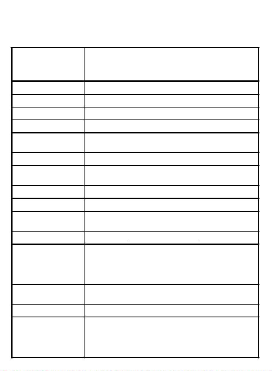
2 Product Specifications
2-1 Specifications
19-inch, (18-inch visual image area) sloted mask, 90 degrees
Picture Tube
Scanning Frequency VGA, Super VGA, 1024x768@75/85 Hz, 1280x1024@85 Hz
Maximum Resolution 1600 dots (H) x 1200 lines (V) @75Hz refresh rate
Display Area 350 mm (H) x 262 mm (V) typical
Display Characters 80 char. x 60 rows on a 10 x 10 matrix
deflection, dot type black matrix, medium short persistence
phosphor, dark tint, non-glare/ anti-static screen,
0.26 mm dot pitch
Display Colors Analog
Input
Synchronizatin Signals Separate Sync: horizontal/vertical, TTL, positive or negative
Synchronization
Frequencies
Signal Connectors 15-pin, D-shell connector
Video Signals Analog : 0.7 Vp-p, RGB positive
Power Input 120 Watts (maximum) AC rated voltage, 100VAC to 240VAC,
Misconvergence Center Area : < 0.3 mm; Corner Area : < 0.4mm
User Controls
Service Controls PWB-1596/1598 : power voltage adjust (VR801)
Unlimited Colors
Horizontal : 30 to 96 kHz
Vertical : 50 to 160 Hz
200VAC to 240VAC for PNST/PNSL models
Power On/Off, Contrast, Brightness, Horizontal Size,
Horizontal Position, Vertical Size, Vertical Position,
Pincushion, Trapezoid, Pin Balance, Parallelogram, Rotation,
Color temperature, Language, Display Frequency, Degauss,
Recall, H. Moire, V. Moire
focus 1 , focus 2
Preset Modes 10 (see Table 2-2. Timing Chart)
Environmental
Considerations
Operation temperature : 5oC to 35oC ambient
Operation Humidity : 20% to 80% ambient
Storage temperature : -40oC to 65oC ambient
Storage Humidity : 5% to 95% (non-condensing)
Altitude : up to3000m above sea level
Page 3
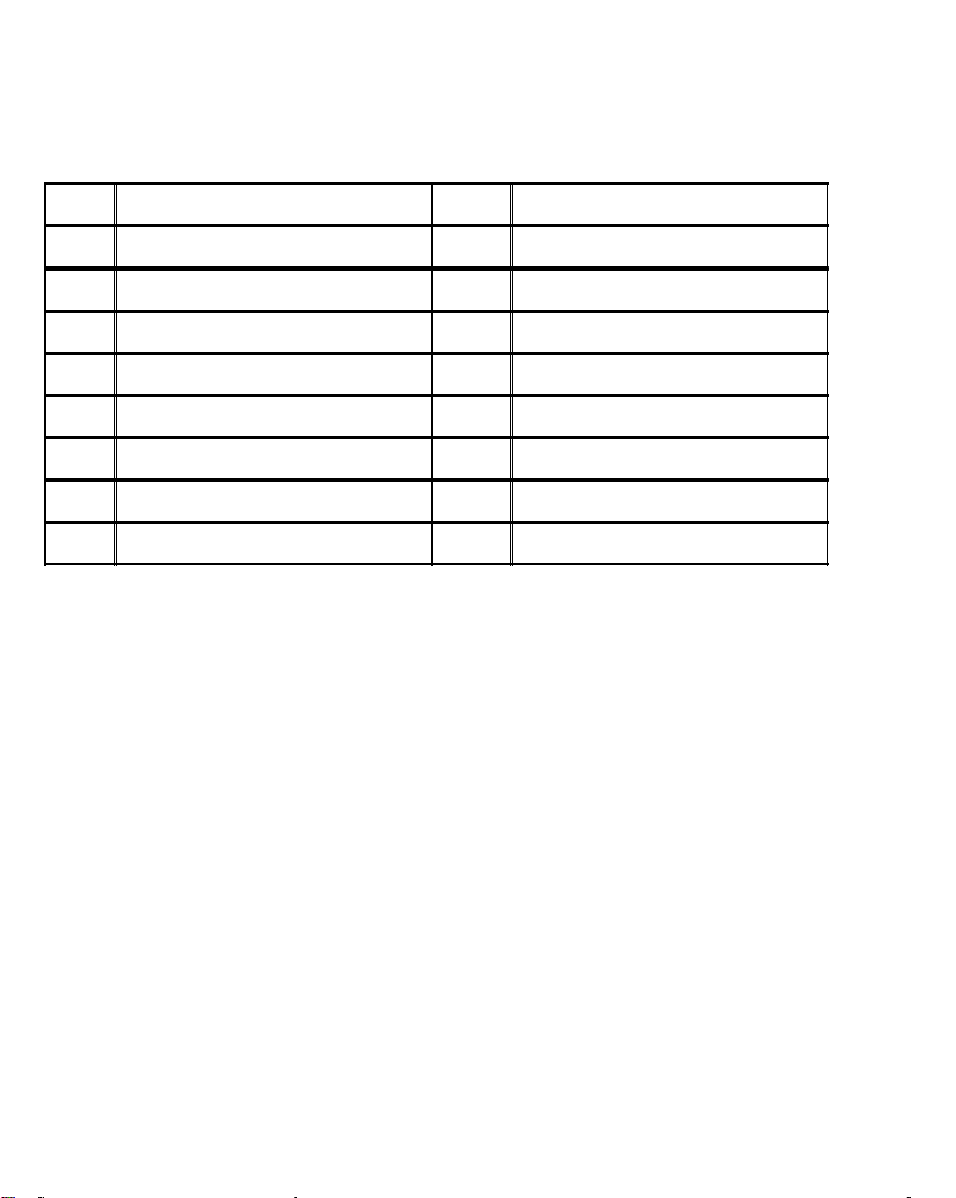
2-2 Signal Cable Pin Connections
Table 2-1. Sig nal Cable Pin Assignment
Pin Signal Pin Signal
1 Red video 9 +5V
2 Green video 10 Digital Ground
3 Blue video 11 Ground
4 Ground 12 SDA
5* Ground 13 H-Sync
6 Red ground 14 V-Sync/VCL
7 Green ground 15 SCL
8 Blue ground
Note: * This pin is used f or selftest detection. Connect this pin to ground at the PC end.
Page 4
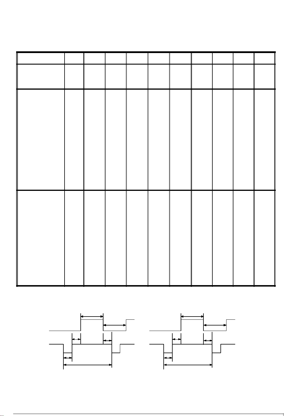
2-3 Tim ing Chart
Seperate Sync
Video
I
J
Sync
GHL
K
This section describes the timings that the computer industry recognizes as standard f or computer-generated
video signals.
Table 2-2. Timin g Chart
Mode 1 2 3 4 5 6 7 8 9 10
H. Dots 640 720 640 832 800 1152 1024 1600 1280 1600
V. Dots 480 400 480 624 600 870 768 1200 1024 1200
H-freq (kHz) 31.47 37.927 43.27 49.725 53.67 68.681 68.67 75 91.146 93.75
Sync Polarity - - - - + - + - + +
A period us 31.78 26.366 23.11 20.11 18.631 14.561 14.561 13.333 10.971 10.667
B Blanking us 6.356 6.085 5.33 5.586 4.409 3.04 3.725 3.457 2.844 2.765
C Sync us 3.81 2.028 1.556 1.117 1.138 1.28 1.016 1.185 1.016 0.948
D B.P. us 1.907 3.042 2.22 3.91 2.702 1.44 2.201 1.877 1.422 1.501
E Active us 25.42 20.282 17.78 14.524 14.222 11.52 10.836 9.877 8.127 7.901
F F.P. us 0.636 1.014 1.556 0.559 0.569 0.32 0.508 0.395 0.406 0.316
V-freq (Hz) 59.94 85 85 74.55 85 75.062 84.99 60 85 75
Sync Polarity - + - - + - + - + +
G Period ms 16.68 11.759 11.76 13.414 11.756 13.322 11.765 16.667 11.761 13.333
H Blanking ms 1.43 1.213 0.67 0.864 0.578 0.656 0.582 0.667 0.527 0.533
I Sync ms 0.064 0.079 0.069 0.06 0.056 0.044 0.044 0.04 0.033 0.032
J B.P. us 1.02 1.107 0.578 0.764 0.503 0.568 0.524 0.613 0.483 0.491
K Active us 15.25 10.546 11.09 12.549 11.179 12.667 11.183 16 11.235 12.8
L F.P. us 0.35 0.026 0.023 0.04 0.019 0.044 0.015 0.013 0.011 0.011
Horizontal
E
Video
D
Sync
B
F
Vertical
H.Parameters:
A: Period B: Blan king Time
C: Sync Width D: Back Porch
E: Active Time F: Front Porch
C
A
V.Parameters:
G: Period H: Blan king Time
I: Sync Width J: Back Porch
K: Active Time L: Front Porch
Page 5

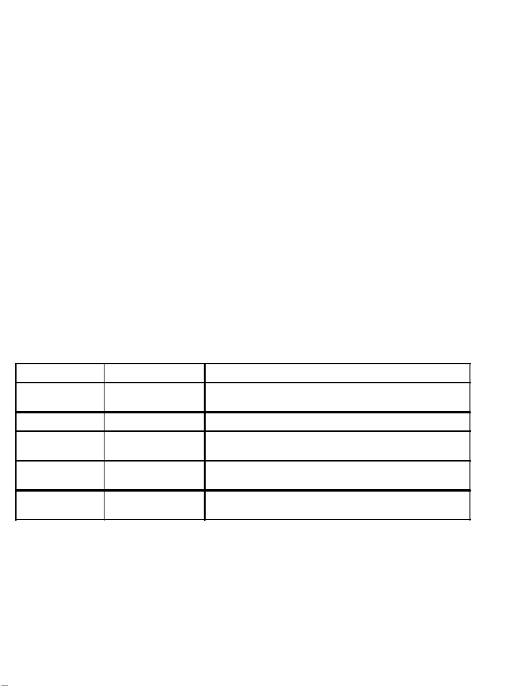
2-4 Power Saving Function
Note: The monitor will be driven into “Power Saving ” mode by the control signal from the display
controller, as indicated by the amber-color power LED.
Table 2-3. Power Sav ing Function
State Power
Consumption
LE D
Light
ON <120 watts Green
Active
OFF
Th e power saving states will be kept until a control signal has been detected or the keyboard or mouse is activated.
Th e recovery time from Active OFF state back to ON state is around 10 seconds.
<3 watts Amber
2-5 TCO Version (Optional)
The monitor meets the TCO 99, NUTEK energy saving, electric and magnetic f ield requirements.
2-5-1 TCO 99 V ersion (Optional)
The emission f rom magnetic and electric field must comply with the limits specified by the Swedish Board
f or Measurement and Testing, commonly known as MPR 1990 recommendations. T hese limits are
summarized in the Table 2-4.
Table 2-4. TCO 99 Requ irements
VLF/TCO ELF/TCO
Magnetic Field 25 nT 200 nT
Electric Field 1 V/m 10 V/m
Frequency Range 2~400 kHz 5~2000 Hz
Value RMS RMS
Distance 30 cm 30 cm
Electrostatic
Potential
+/- 500 V +/- 500 V
Page 6
The monitor is de signed with selected CRT and carefully routed wires around CRT, make sure exactly the
same routing s cheme is used when doing CRT replacement.
The TCO 99 scheme is f or international and environmental labelling of personal computers. The labelling
scheme was developed as a joint ef fort by the TCO (The Swedish Confederation of Professional Employ
ees), Naturskyddsf oreningen (The Swedish Society for Nature Conservation) and NUTEK (The National
Board f or Industry and Technical Development in Sweden).
1)`Scope
TCO 99 touches on ergonomic qualities, emissions (electrical and magnetic f ields), energy efficiency and
ecology (with demands f or environmental adaptation for both the product and the production processes at
the manuf acturing plant).
2) Environmental Requirements
The monitor abi des by the environmental demands concerning restrictions on the presence and use of
hea vy metals, brominated and chlorinated flame retardants, CFCs (freons), and chlorinated solvents,
among other things. The monitor is also recyclable.
3) Energy Requirements
The monitor als o follows the energy requirements that, after a certain period of inactivity, the monitor
shall reduce its power consumption to a lower level in one or more stages.
4) Others
The monitor me ets the strict environmental demands for the reduction of electric and magnetic fields,
physical and visual ergonomics and good usability.
Table 2-5. TCO 99 Visual Ergonomics
Feature Standard Description
Linearity 1% or less Difference in length of columns or rows compared to the
corresponding lengths through the center of the monitor.
Display Luminance 100 cd/m2 (at least)
Luminance
Uniformity
Color temperature
variation
Reclections from
casing
1.5:1 or less The ratio is between the max to min luminance within the
whole active area.
? u'v' 0.01≦
20% / 30g la ss≧ ≦ The reflection ration is on cabinet & table.
Page 7
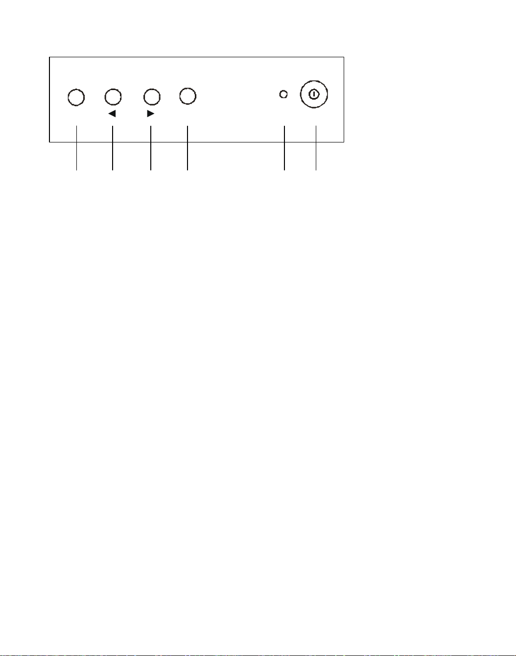
3 Control Location and Functions
1
2
(1) Function Key
(2) Decrease Key
(3) Increase Key
(4) Select Key
(5) Power LED
(6) Power ON/OFF
(1) (2) (3) (4) (5) (6)
3-1 Front Panel
3-2 Front Panel K eys Functions
1. Function Key: Display the main menu, and exit the adjustment screen and save adjustments.
2. Decrease Key: Scroll across main menu, highlighting control to be adjusted. Decrease value of selected
control. Toggle between Contrast and Brightness adjustment screens.
3. Increase Key: Scr oll across main menu, highlighting control to be adjusted. Increase value of selected
control. Toggle between Contrast and Brightness adjustment screens.
4. Select Key: Press once to display adjustment screen. Press again, f or some controls, to toggle between
controls shown in pairs on main menu.
5. Powe r LED: Display different modes (ON, OFF) of the monitor by showing different color for each
mode.
6. Power ON/OFF: To turn the monitor ON and OFF .
3-3 Adjustm ent Procedure
1. Press (6) key to turn on the monitor.
2. At normal condition, press (1)on the f ront panel to activate the on-screen manager (OSM) menu.
3. To select a user control, press (2) or (3) key repeatedly until the control is highlighted.
4. To adjust the value for a particular control, press (4), then press the (2) or (3) key to obtain the desired
value. Th ere are a few parameters that do not require any adjustment, like Manual Degauss, Memory
Recall.
5. Some controls are grouped in pairs on the main menu. Press (4) key to toggle between them.
6. To save your adjustments and exit screen, press (1) key. The menu will automatically clear out f rom the
screen if no keys are pressed within 30 seconds.
Note: To enter the “Internal Adjustment” mode, press (1) & (4) keys simultaneously then press (6).
Page 8

4 Operation Theory
Thi s is a fully digital controlled multi-sync color monitor that is compliant with DD C1/2B Plug and Play
VESA standard and of fers the following main features.
4-1 Main Features
1. Simplif ied design with minimum components.
2. The NOV ATEK NT68P65AU processor-- that has I2C bus controlled geometric correction, contrast and
brightness-- of fers the functions for: (a) Contrast, (b) Brightness, (c) H-size, (d) H-position, (e) V-size, (f)
V-position, (g) Pincushion, and (h) Trapezoid, (i) Pin Balance, (j) Parallelogram.
In addition, it also of fers more functions as: (a) Sync. processor, I/P and O/P, (b) Mute, (c) Power saving
of f, (d) Power saving override, (e) DDC2B, (f) I2C Bus f or auto-alignment through signal cable (g) CS
switching f or linearity and size compensation, (h) High voleage adjustment, (i) G2 voltage adjustment.
3. Stores up to 10 f actory preset modes and offers 6 user modes. There are 18 function icons in OSD. They
are controlled by 1 2 keys on the f ront panel.
4. Powerf ul PHILIPS TDA4841 and TDA4863 present the following useful functions: (a) Pincushion, (b)
Trapezoid, (c) V-Position, (d) V-Size, (e) Vertical’s “C” and “S” correction -- factory adjust, (f) Pincushion’s
V. position cor rection, (g) Corner correction -- factory adjust, (h) Pincushion unbalance correction -f actory adjust, (i) Parallelogram distortion -- factory adjust, (j) Moire cancellation, (k) X-ray protection,
and (l) Full horizontal and vertical auto sync capability.
5. Sof tware controlled auto shut off function activated if fH < = 29 kHz and fH > = 96 kHz.
6. Full range AC input and simplif ied line filter design.
4-2 Microcontrol Section
1. This monitor uses NO VATEK NT68P65AU CPU. It contains a 8-bit CPU core, 256 bytes of RAM used
as working RAM and stack area, 24k bytes of OT P ROM, 14-channel 8 bit PWM D/A converter, 2channel A/D converters f or key detection saving I/O pins, internal H. sync and V. sync signals processor
providing mode detection, and an I2C bus interf ace. When H/V sync through D-Sub signal cable enter pin
41 and pin 42, the CPU perf orms frequency / polarity detection and calculate and send to H/V sync OUT.
Then C PU reads the data from I703 and transfer to device 4841 and some DAC in CPU, above operation
takes about 500 ms.
2. There allows 10 factory preset modes and 6 user modes. There are 8 f unctions, Contrast, Brightness, H.
Size, H. Position, V. Size, V. Position, Pincushion, and Trapezoid, all controlled by OSD icon which can
be adjusted by user.
3. The pin 25 and pin 26 are used f or ATE function. When CPU receives C6 as slave address, it will operate
in A TE mode which is use d for auto-alignment. After alignment the data will be stored in I703.
4. The us er control parameters are selected by OSD icons, through 1 2 keys , they are detected by
sensing the voltage through R710, R759, R713, R714, R709, R711, R760 to pin 16 and 17 of I701.
4-3 Deflection Section
1. I2C -- autosync def lection controller is TDA4841.
2. The TDA4841 is a high performance and efficient solution for autosync monitors. All functions are
controllable by I2C bus. SDA and SCL signals coming f rom microprocessor feed to pin 19 and pin 18 to
control all f unctions.
Page 9

4-3-1 Horizontal Section
1. The oscillator is driven by the currents in R472 and R468. The minimum oscillator f requency is determined
by R472 and the maximum f requency is determined by R468.
2. Horizontal sync goes into pin 15 through R494. And horizontal f lyback pulse goes into pin 1 through R479
and bypass filter C445 from Emitter of Q407 and C412, C433, C411, R419, C456, R421, D413 for AFC
loop.
3. Horizontal driver (pin8) output to Q401 via C401, Q 401 switching to drive T401 provide IB1/IB2 current
then turn on/of f Q402 and switching the yoke current.
4-3-2V ertical Section
1. V ertical sync goes into pin 14 through R493.
2. The f ree running frequency is determined by R470 and C442.
4-3-3 V ertical O/P section
1. The dif ferential output currents from pin 13 of Vout1 and pin 12 of Vout2 can be directly coupled to the
vertical def lection booster pin 3 and pin 2 of TDA4863.
2. The TDA4863 has two output stages which are current driven in opposite phase and operate in combination
with the def lection coil in a half bridge configuration.
3. This IC is powered by three sets of positive voltage. (+13V at pin1, 37V at pin 8, -13V at pin 6)
4-3-4 E-W/T rapezoid and H. Width Controls
1. The scan current is determined by B+ (the voltage of C413) that is obtained from step down circuit
output. Step down circuit include Q404, T402, D407.
2. I401 TDA4841 pin 6 (B DRV) will drive the step down circuit to change H. width.
3. EW DRV (pin 11) provides a complete EW drive waveform including parabola, corner and trapezoid
correction and f eed to BIN (pin 5 of I401) to get a good control for pincushion / trapezoid / corner.
4. The top and bottom corner correction can be adjusted seperately.
4-3-5X-Ray Protection
1. To avoid X-ray hazard, a DC voltage generated at pin 6 of FBT and rectified by D107, C111 and divided
by R476, R477 and R478 come into pin 2 of TDA4841.
2. If this voltage is higher than 6.39 V, then T DA4841 w ill be activated to float HUNLOCK (pin17), H.
DRV( pin 8), B DRV (pin 6), VOUT1 (pin 12), VOUT2 (pin13). After that all deflection circuit stop
working.
4-3-6 Blanking and Brightness
1. The verti cal blanking signal comes from I401 pin 16 and vertical sync. These two pulses combine into
Q542 and Q541. This signal f eets into T501 pin 24.
2. In protection mode or out of range or mode change mute signal will turn high and turn on Q107.
G2 voltage will drop f rom 600V to 250V.
3. The brightness is control by I2C bus. The output pins are I501 pin 14, pin 15, pin16.
Page 10

4-3-7 Contrast Section
1. Contrast is controlled by I701 through I2C bus to I501 (LM1267) directly.
2. Beam current is detected through T 101 (FBT) pin 7, D106, C109, Q102, R108, R121, R122 to control
I501 pin 22 voltage. When I501 pin 22 voltage drops below 5V, the ABL f unction will happen.
4-3-8 Dynamic focus circuitry
The dy namic focus is applied to improve the corner focus performance, it includes horizontal and vertical
dynamic f ocus.
1. V ertical dynamic comes from I401 pin 32 and is amplified through C105, Q101, C137, and feed to FBT
dynamic f ocus pins R133, R132, Q101.
2. This amplif ier need 200V voltage supply, it comes from FBT pin 8 and rectified through L102, D101, and
C102.
4-4 Power Supply Section
4-4-1 AC Rectifier
The circuit can accept 90 V to 264 V AC input through D801 bridge diodes and C808 f iltering to get DC 126
V~364 V f or power conversion in T802.
4-4-2 Line F ilter
It consists of C801, C802, C803, C816, C820, C823, T801, T804 and meets EMI regulation.
4-4-3 Pow er LED Status
1. The LED has 3 leads with common cathode to emit green and amber color light for different power
saving states.
2. Normal : Green light
3. Of f Mode : Amber light
4-4-4 Auto Degaussing
When S801 turns on, pin 27 of I701 will send a signal to Q802 and turns on RL801 for degaussing. After 4
seconds, it will turn of f RL801 automatically.
4-4-5 PWM Control
1. Start Up
The I801 (KC3843B) gets power from R846, Q821, R849, R 848, D826, D828, D822 and pin 7 voltage
reaches 8 V f or starting up. The I801 starts oscillation at 22 kHz, sawtooth on pin 4 and pin 6 output to
drive Q803/T802. Once Q803 s witching on, D806, C804 set up an 15 V to keep I801 working through
D821 auxiliary voltage.
2. Regulation
The DC O/P voltage is proportional to the auxiliary voltage, so I801 pin 2 senses the feedback voltage
f rom the divider R802, R823, VR801 and R820 to compare with the built-in 2.5 volts reference voltage for
error amplif ier operation. Finally pin 6 can modulate the different duty cycle by VR801 setting to achieve
regulation purpose.
Page 11

4-4-6 Synchronization
1. Normal Mode
The sync pulse from FBT (31 kHz~95 kHz) via R812, R831, C815, R826, D824, C814 and R816 to pin 4
of I801 to keep I801 synchronized with horizontal sync input frequency.
2. Power Saving Modes: Of f mode
Becau se there is no pulse from FBT, so the free-run frequency is decided by R817 and C814 and the
SMPS works at 22 kHz.
3. Override
The horizontal f ree run frequency is about 62.5 kHz under override condition, SMPS is synchronized to
this f requency.
4-4-7 O.V.P.
If the auxiliary voltage is higher than zener voltage ZD807 (20 volts) and makes pin 3 of I801 higher than
1 V, pin 6 duty cycle is limited to have the OVP activated.
4-4-8 O.P.P.
The excess current of T802 through R813, R814, R834, C813, R865 and R864 can develop enough voltage
on pin 3 then limit the power delivered because the pin 6 duty cycle is limited too.
4-4-9 High Voltage Generation w ith F.B.T.
1. The H. V generation circuit combines T101 F.B.T. with I101 TL494/KA7500 PWM control circuit.
2. When I 101, Vcc(pin12) reaches at 12V, pin 5,6 gets a freerun sawtooth waveform about 25KHz, and
approximately 5.7Vp-p, when voltahe at pin 15 is higher than pin 16 (5V ref erence) then release pin 3 to
be controlled by pin 1 f eedback signal and compare with pin 5 to output PWM.
3. HFLB1 is used to trigger pin 5 via Q112, to synchronize the def lection circuit.
4. PWM output will drive Q116 & T101 to gererate high voltage (26KV), T101 pin 11, 15 becomes DC/AC
f eedback, with the voltage link to I101 non-inverting input pin 1 to stabilize H.V (26KV) and VR101 can
be adjusted to control H.V value.
5. When X.R.P occur, the hunlock will keep high to pull down I101 pin 2 and shut down PWM output.
4-5 Video Am plifier Section
1. RGB s ignal inputs are terminated by R501, R531 and R561 then pass through the coupling capacitors
C501, C531 and C561 to IC501 LM1267 preamplif ier.
2. The amplif ier RGB signals (0~4 Vpp) are adjusted by I2C bus f rom I501, pin 23 is for clamp pulse which
comes f rom pin 16 of TDA4841.
3. The video output stages are amplif ied by I901(LM2465). The RGB cathodes cut off are adjusted by I2C
bus control by internal icon.
4. Under override condition, “CHECK SIGNAL” will show up on the screen.
4-6 OSD (On Screen Display) Circuit
Page 12

AC9 01
1. The I502 NT6827-00002 is OSD IC. The OS D signals are worked by positive vertical pulse from I701 pin
32 that goes through R554 to I502 pin 10, and positive horizontal pulse f rom HFLB1 through R527 to I502
pin 5. CPU I701 pin 27, 28 (I2C bus) transf ers information to I502 pin 7, 8.
2. The OSD R. G. B signals and blanking signal are terminated at I502 pin 15, 14, 13, and 12 f eed into I501
pin 1,2,3, and 4, then the OSD picture appears.
Page 15
Page 13

5 Alignments and Adjustments
This section of the service manual explains how to make permanent adjustments to the monitor settings.
5-1 General Adjustm ents
5-1-1 Adjustment Conditions
a) Power Supply
Apply AC 115 V or 220 V
b) Warm-u p Time
The monitor must be powered on f or 15 minutes before starting any alignment, but requires 30 minutes of
warm-up time f or convergence adjustment.
c) Signal Input
1. Video: RGB Analog, 0.7 Vp-p, positive
2. Synchronization: Horizontal and vertical TTL signal, separate, positive or negative
3. All adjustments should be made using a signal of FH = 91 kHz, FV = 85 Hz, unless otherwise defined.
5-1-2 Equipment Required
The f ollowing equipments are necessary for adjustment procedures:
1. V olt-ohm-A meter (Sanwa F D-750C or equ ivalent)
2. 30 kV high voltage probe (HP34111A)
3. Oscilloscope (TEK2235 or equivalent)
4. Minolta Color Analyzer II
5. Signal generator (COMPAQ PC with proper display cards or Chroma 2250//2225)
6. Screwdriver
5-1-3Sw itching Power Supply and Regulator Adjustment
a. The regulated B+ control has been preset in the f actory and needs no adjustment. However, if any repair
is made on the power supply section, the f ollowing readjustment procedures are recommended:
1. Allow the monitor to warm-up f or about 15 minutes.
2. Apply XGA (1280 x 1024 @ 91 kHz/85 Hz) signal to the monitor.
3. Connect a DC voltage meter to TP001 end, and adjust VR801 f or 10.7 + 0.1 V DC
4. If a fuse is broken during adjustment, remember to replace it with the exact same type of fuse.
b. If necessary, follow the following procedures to enter the factory mode.
1. Press both 1 key and 2 key simultaneously then power On.
2. Af ter turn the power off, monitor will go back to normal mode.
Page 14

5-2 Alignm ent Procedures
5-2-1 High V oltage Adjustment
CONDITION
Display image : Crosshatch pattern
5-2-2 Screen and White Balance Adjustment
CONDITION
Press 1 and 2 buttons simultaneously when switching the power “On”.
Display image : No video
PROCEDURE
1 Raster color setting
1-a Adjust HV icon to set high voltage = 26KV.
1-b Adjust G2 icon to set G2 at 600 ± 5V
1-c Set Brightness icon maximum to 40%
1-d Select OSD icon to R.G.B. cutof f
1-e Set G gun cutof f to 0.5 ± 0.15 FL
1-f Adjust R/B cutof f to get x=283 ± 5, y=297 ± 5, Y=0.6 ± 0.2 FL
1-g Set Brightness to cutof f , get Y=0.01 ~ 0.03 FL
1-h Set Brightness to minimum.
CONDITION
Display image : 50 mm x 50 mm white block pattern
PROCEDURE
2 65000K color temperature setting
2-a Set Brightnes s to cutoff and Contrast to 75 Value
2-b Move cursor on OSD to choose color temperature icon.
2-c Press 2 key to G gain then adjust G gain = 70 value, then adjust B, R to x=313±5, y=329±5.
2-d Check x=313±5, y=329±5.
3 93000K color temperature setting
3-a Move cursor on OSD to choose color temperature icon.
3-b. Press 2 key to G gain then adjust G gain = 75 value, then adjust B, R to x=283±5, y=297±5.
3-c Adjust Contrast max. to set Y=38±2FL
3-d Check x=283±5, y=297±5.
3-e Adjust Contrast min. to set Y=1.0FL.
4 Full white ABL setting
Page 15

CONDITION
Display image : f ull white pattern
4-a Set Brightness to cutof f and Contrast to maximum.
4-b Move cursor to choose ABL inside contrast icon.
4-c Adjust ABL to set Y=32±1FL
4-d Repeat all the procedures in 5-2-2 section until the best white balance is obtained.
5-2-3 Focus Adjustment
CONDITION
Display image : “e” character pattern
PROCEDURE
1. Set Brightness to cutof f and Contrast to maximum.
2. Adjust top VR at T101 (static f ocus VR) to make vertical line clear.
3. Adjust center VR at T101 (dynamic f ocus VR) to make horizontal line clear.
4. Repeat above procedures to get best f ocus.
5-2-4 Dynamic focus Adjustments
1. Horizontal dynamic f ocus set Hf=370V ±10 V in phase (compare with Vcp signal).
2. V ertical dynamic focus set Vf=145V ±10V in phase.
5-2-5 Static Convergence Adjustments
Static convergence involves alignment of the red, blue and green lines in the center area of the display.
Note : The monitor requires 30 minutes warm-up time f or convergence adjustment.
CONDITION
Page 16

Display image : Crosshatch pattern
Red/
movement
movement
Warm-up Time : 30 minutes
PROCEDURE
1. Set Brightness and Contrast to display a well-def ined pattern.
2. Ensure the convergence magnet rings are correctly positioned on the CRT.
Fig ure 4-1. Convergence Magnets on the CRT
1
11
+
P
CRT
FRONT
87 65 4 3 2
10
1) Setup Bolt 2) Bow Magnet 3) Band
5) Spacer 7) Spacer
6) 6-Pole Magnet
9) Holder
9
4) 4-Pole Magnet
8) 2-Pole Magnet
11) Tabs10) Band
3. Rotate the individual rings of 4-pole convergence magnets by changing the spacing between the 2 tabs to
converge the vertical red and blue lines at the center of the screen.
4. Rotat e the pair of rings of 4-pole convergence magnets by maintaining spacing between the 2 tabs to
converge the horizontal red and blue lines at the center of the screen.
5. Rotate the individual rings of 6-pole convergence magnets by changing the spacing between the 2 tabs to
converge the vertical red, blue and green lines.
6. Rotat e the pair of rings of 6-pole convergence magnets by maintaining spacing between the 2 tabs to
converge the horizontal red, blue and green lines.
7. Repeat the steps f rom 3~6 until the best convergence is obtained.
Note : The 4-pole magnets and the 6-pole magnets interact, making dot movement complex.
Blue
Red
Fig ure 4-2. 4-pole and 6-pole Magnets Movement
Blue Red
4-pole magnets
Blue Green
Red/
Blue
Green
6-pole magnets
Page 17

5-2-6 Degaussing
Degau ssing is required when poor color impurity appears on the screen. This monitor uses an automatic
degaussing circuit that is activated when the power is on. The automatic degaussing will be f ully functional
again af ter the monitor has been in operation for 20 minutes.
The degaussing effect is confined to the picture tube since the coils are mounted at the back of the tube.
Should any part of the chassis or cabinet becomes magnetized, it is necessary to degauss the affected area
with a manual degaussing coil.
5-2-7 Manual Degaussing
1. Apply line voltage to the degaussing coil and move it in a rotary motion over the f ront, sides, and top of the
monitor. The coil should be kept away f rom the rear of the monitor to avoid damaging the magnetic neck
components.
2. Slowly rotate and move the coil away f rom the monitor to about 6 feet beyond the point where no effect
on the CRT will be noticeable.
For proper degaussing, it is essential that the f ield be gradually reduced by moving the coil slowly away from
the monitor. The degaussing coil must never be shut off or disconnected while near the monitor, as this would
introduce a strong f ield instead of canceling the effect of the stray fields.
Page 18

6 Troubleshooting
6-1 No Raster
No Raster
Measure
voltage of B+ at
T402 pin 2 on
PWB-MAIN
0 V
Short Circuit
at load?
Yes
Check DC B+ line,
Q402, Q404
(137 V, 91kHz)
Check voltage of
No
Check I801,
Q803, R814,
R813, ZD807,
ZD801, R811,
R861, D825
cathode, heater, Grid
Check
AC I/P on
C808
Yes
Normal
1, Grid 2, etc.
No
D801,T801,
R804, T804,
High
(175 V or more)
Check I401
Check
F801
Page 19

6-2 OSD Abnorm al
OSD Abnormal
Check I502
missing?
No
Check R516,
R526, R527
OK?
Yes
Check J516,
R556 OK?
Yes
Yes
No
No
Put on
I502
Replace them
Replace it
Replace I502
Page 20

6-3 Function K ey Abnormal
Function Key Abnormal
Check I701 and
I703 missing?
No
Power
ON/OFF again and
check X701, oscillator
OK?
Yes
Check
I703 EEPROM content
OK?
Yes
Yes
No
No
Put on
I701, I703
Replace X701
Replace I703 or do
ATE again
Replace I701 and check
uP OK?
No
Check
pin 5 of I701
is 5V?
No
Replace I705
Yes
Yes
Replace I701
Check
R732, C713
Page 21

6-4 No Vertical Scan (Raster is one horizontal line)
No Vertical Scan
Check
I301 voltage of
pin 1 is 12V, pin
2 is 37V and
pin 4 is
-14V?
Yes
No
Check or replace
I301.
Check
pin 5 O/P waveform
at I301
Normal
Check
pin 6, 7 of I301
waveform
Still no vertical scan
Check or replace CRT
Abnormal
Replace I301
Page 22

6-5 Out of Horizontal Synchronization
Out of Horizontal
Synchronization
Horizontal
sync present at
pin 15 of I401
Yes
Check
I401 pin 8 H output
frequency
Yes
Check Q401, T401,
Q402, R402, R403,
C404, R404, D402, Q410
6-6 Out of Vertical Synchronization
Out of Vertical
Synchronization
No
No
Ckeck or replace
the signal cable or
I701
Check or replace
the signal cable
or I701
Vertical sync
present at
pin 14 of I401
Yes
Check
I401 pin 24 ramp
frequency
Check C442
No
Ckeck signal cable &
vertical sync input &
I701
Page 23

6-7 R.G.B. Video Am plifier Abnormal
RGB Video AMP Abnormal
Check
waveform at I501 pin 18, 19
and 20
Yes
Check
I901 pin 1, 3 and 2 voltage
and wave form
Yes
Video signal present at the
pin of the CRT R.G.B.
Cathode
Yes
Check or replace the
No
signal cable or I501
No
Replace I901
Defective cut-off circuit
(DC restore)
6-8 Blank EEPROM Trouble-shooting:
Description o f functions for models under C1996 series EEPROM DATA AUTO-RELOAD
Th e function allows plant staff to pre-write and customer service personnel to use blank EEPROM
through th e pre-write EEPROM function whenever the CPU is implemented. The method of operation
is as f ollows:
Fi rst, press the H OT KE Y, start af ter C1996 turns to (<&>) KEY . At this point of time, the CPU
i s capable of detecting the f irst 8 D ATA of each page that E E P R OM contains. When the
r eading goes to 00H or FFH, the EEPROM PAGE will turn to blank; instead, the pre-set value
i s being w ritten into the E E PR OM through CP U . Otherw ise, it shall be deem ed an eff ective
value and that the pre-write f unction shall not be activated.
Page 24

7 Recommended Parts List
Note:1. The components identif ied by “ “ mark are critical for X-ray safety. Replace these with
exactly the same parts specif ied.
2 . There is only OTP IC at the model beginning (FPR stage or bef ore). When it put in mass
production and there must be Mask coming out. Please check BOM to get the last release part
number and related inf ormation.
No. Location Part Number Description
1 C407 6325943252-03 P=22.5 PPS 4300P 1800V
2 C808 6312633126 ALU uF 330 400V F 85C 25x40
3 D801 6417001000 TS4B05G-01
4
5
6
7
8
9
10
11
12 I802 6442014000 IC LTV-817D
13 T404 6139000500 XFRMER H-CENT THC1005 5mH
14 *** Q402 6421004310 TR NPN 2SC5411 (TOSHIBA)
15 *** Q404 6427000900 FET P-CHNL SFS9634
D814 D815
D402
D407
D817 D119
D831 D813 6412002937 DIODE FUF 5407AMP 3A/800V
**
F801 6851504053 / 51 FUSE TIME LAG 5ST4 4A/250V
**
I301 6442026400 IC TDA4863 9P (PHILIPS)
***
I401 6442030000 IC TDA4841 32P SDIP (PHILIPS)
**
I501 6442031500 IC LM1267
**
I701 6448017800 IC NT68P65AU 42P PDIP NOVATEK(FLASH)
**
6412020007 DIODE SF34 3A/200V
6412014707 PUP5406
16 *** Q116 6426005410 FET N-CHNL IRFS840A
17 Q115 6426006400 FET N-CHNL IRFS630A SAMSUNG
18
19 R803 6203459017 POSISTOR 4.5 OHM Q 2PINPITCH=10
20 R804 6201100062 THERMISTOR 10 OHM 5A P=7.5 TKS
21 *** R818 6422002925 FS OHM 0.27 1W J HOR
22 T401 6135003400 XFRMR HOR DRIVE THD-1034 EI19
Q803 6426009600 FET N-CHNL 2SK2996 TOSHIBA
***
Page 25

No.
23 T101 6133093010 FBT TFB-9301 FM159R-B
24 T402 6111444130 COIL CHOKE 4.4MH
25 T801 6138002201 LINE FILTER TLF-1016A 16mHET28
26 T802 6131052500/510 XFRMER PWR TPW-1087 EE40
27 X701 6449006900 CRYSTAL 12MHz TOP8.000 30pF TOP
28 ** I901 6442032300 LM2465 9P
29 I402 6442005900 LM324 14P
30 *** I801 6442006720 KA3843B
31 I301 6442026400 IC TDA4863 9P (PHILIPS)
32 R813 6221215852 0.15 OHM 2W
33 ** I703 6448015720 MICRO CHIP IC 24LC08B-8P
34 D818 6412019907 SF24
Location Part Number Description
35
36 C413 632627456-03 MPP 0.27U 250V TAI PMS
37 C421 6326210453-03 MPP 0.1u 250v TAI PMS
38 C423 6326322443 MPP 0.22u 250V HJC
39 C425 6326262442 MPP 0.62u 250V HJC
40 C427 6326215542 MPP 1.5u 250V HJC
41 V901 6811192608 M46QCE261X112 SAMSUNG
Q406 Q410
Q403
6421003800 KSD882
Page 26

V
Blanking
Q541
Q542
P501
B-IN
R-IN
G-IN
B
VIDEO PREAMP
B
R
G
R G
LM1267
CLBL
R G B
I502
NT6827
OSD
5V
HFLB1
VTTL
ABL
SCL1
SDA1
HFLB1
CLBL
LM2465
RGB
CUT OFF
ADJUST
Q901
Q902
Q931
Q932
Q961
Q962
Q903
Q933
Q963
HEATER
R
G
B
G1 G2
FOCUS 2
HV
FOCUS 1
P702
SCL
SDA
DDC 5V
P502
LED
CLBL
HFLB
SDA 1
SCL 1
V SYNC
H SYNC
O/R
SCL
SDA
KEY
CONTROL
VTTL
HFLB1
6.3V
G2 CONTROL
I701
NT6861 AU
VIDEO 5V
GENERATOR
VTTL
HTTL
SCL1
SDA1
OFF
CLBL
10.7V
80V
GND
I401
TDA 4841
10.7V
10.7V
180V
VOUT 1
VOUT 2
P505
PWM CONTROL
TL494/KA7500
HFLB1
D. FOCUS
XRP
C137
R132
+H
-H
+V
-V
200V
48V
G2
G2 CONTROL
CONTROL
CKT Q105
Horizontal
Dynamic focus
DY
ABL
P301
I101
Q116
FBT
DRIVER
Q115
CANCELING
CKT
T101
FBT
80V
LINEARITY
CONTROL
T403
T102
H DRIVER
Q402
D403
C407
B+
DRIVER
Q404
T402
V
DYNAMIC
180V
H CENTER
Q403
VR401
XRP
CKT
P801
D701
4.3V
D703
SCL1
SDA1
5V
Q807I705
13V
L
N
LINE
FILTER
BRIDGE
DIODE
FG
E2PROM
LOW VOLTAGE
DROP DOWN
2404
I703
DEG
CKT
I801
SMPS
VERTICAL
O/P
I301
TDA4863
-14V
POWER
O/P
T802
-14V
80V
180V
10.7V
37V
13V
10.7V
10.7V
SWITCH
7V
Q813
13V
 Loading...