

Page 1

Copyright and Warranty Notice
The information in this document is subject to change without notice and does not
represent a commitment on part of the vendor, who assumes no liability or
responsibility for any errors that may appear in this manual.
No warranty or representation, either expressed or implied, is made with respect to
the quality, accuracy or fitness for any particular part of this document. In no event
shall the manufacturer be liable for direct, indirect, special, incidental or
consequential damages arising from any defect or error in this manual or product.
Product names appearing in this manual are for identification purpose only and
trademarks and product names or brand names appearing in this document are the
property of their respective owners.
This document contains materials protected under International Copyright Laws. All
rights reserved. No part of this manual may be reproduced, transmitted or
transcribed without the expressed written permission of the manufacturer and
authors of this manual.
If you do not properly set the motherboard settings, causing the motherboard to
malfunction or fail, we cannot guarantee any responsibility.
Page 2

Page 3

SL6 Motherboard User’s Manual
TABLE OF CONTENTS
CHAPTER 1. INTRODUCTION OF SL6 FEATURES
1-1. F
1-2. S
1-3. L
1-4. T
CHAPTER 2. INSTALLING THE MOTHERBOARD
2-1. I
2-2. I
2-3. I
2-4. C
EATURES OF THIS MOTHERBOARD
PECIFICATIONS
AYO UT DIAGRAM
HE SYSTEM BLOCK DIAGRAM
NSTALLING THE MOTHERBOARD TO THE CHASSIS
NSTALLATION OF THE PENTIUM
NSTALLING SYSTEM MEMORY
ONNECTORS
EADERS AND SWITCHES
, H
III CPU 2-3
Index
1-1
1-2
1-4
1-5
2-2
2-4
2-6
CHAPTER 3. INTRODUCING THE BIOS
3-1. CPU S
3-2. S
3-3. A
3-4. A
3-5. I
3-6. P
ETUP
TANDARD
DVANCED
DVANCED CHIPSET FEATURES SETUP MENU
NTEGRATED PERIPHERALS
OWER MANAGEMENT SETUP MENU
3-7. PNP/PCI C
3-8. PC H
3-9. L
3-10. L
3-11. S
3-12. S
3-13. E
EALTH STATU S
OAD FAIL-SAFE DEFAULTS
OAD OPTIMIZED DEFAULTS
ET PASSWORD
AV E
& E
XIT WITHOUT SAV I N G
[SOFT MENU
CMOS F
EATURES SETUP MENU
BIOS F
ONFIGURATIONS SETUP MENU
XIT SETUP
™
II] 3-4
EATURES SETUP MENU
3-12
3-16
3-21
3-25
3-32
3-41
3-44
3-46
3-46
3-47
3-49
3-50
APPENDIX A INF INSTALLATION FOR WINDOWS® 98 SE
APPENDIX B INSTALLING THE VGA DRIVER FOR WINDOWS® 98
SE
APPENDIX C INSTALLING THE AUDIO DRIVER FOR WINDOWS
98 SE
APPENDIX D ATA INSTALLATION FOR WINDOWS® 98 SE
MN-200-2A0-81 Rev. 1.00
®
Page 4

APPENDIX E INSTALLING THE VGA DRIVER FOR THE
WINDOWS
®
NT 4.0 SERVER / WORKSTATION
APPENDIX F INSTALLING THE AUDIO DRIVER FOR THE
WINDOWS
®
NT 4.0 SERVER / WORKSTATION
APPENDIX G ATA INSTALLATION FOR THE WINDOWS® NT 4.0
SERVER / WORKSTATION
APPENDIX H INF INSTALLATION FOR THE WINDOWS 2000
SERVER / WORKSTATION
APPENDIX I INSTALLING THE VGA DRIVER FOR THE
WINDOWS 2000 SERVER / WORKSTATION
APPENDIX J INSTALLING THE AUDIO DRIVER FOR THE
WINDOWS 2000 SERVER / WORKSTATION
APPENDIX K ATA INSTALLATION FOR THE WINDOWS 2000
SERVER / WORKSTATION
APPENDIX L BIOS FLASHING USER INSTRUCTIONS
APPENDIX M HARDWARE MONITORING FUNCTION
(INSTALLING THE WINBOND HARDWARE
DOCTOR UTILITY)
APPENDIX N INSTALLATION GUIDE FOR SUSPEND TO RAM
APPENDIX O TROUBLESHOOTING (NEED ASSISTANCE?)
APPENDIX P HOW TO GET TECHNICAL SUPPORT
Page 5

Introduction of SL6 Features 1-1
Chapter 1. Introduction of SL6 Features
1-1. Features of This Motherboard
The SL6 Motherboard is designed for use with Intel’s new generation of Pentium Processors
which utilise the FC-PGA (Flip Chip Pin Grid Array), 370-pin design. Up to 512MB of
memory can be supported.
The SL6 uses the new Intel 815 chipset. Its’ 133 MHz capable memory interface supports
the wide range of PC 133 memory devices now on the market. Its 133MHz capable front-
side bus delivers a clear upgrade path to the future generation of 133MHz processors. The
SL6 has built-in Ultra ATA/66. This provides speedier HDD throughput that boosts overall
system performance. Up to four IDE devices can be supported by your system. These can
be either Ultra ATA/33 IDE devices or Ultra ATA/66 IDE devices.
A Digital Video Out Interface supporting digital display and TV Out are options. The SL6
also has an integrated AC ‘97 2.1 CODEC onboard. This CODEC is complete with a H/W
Sound Blaster Pro
compatibility. The chipset includes integrated 2X 3D Graphics Acceleration. For those
wanting even greater graphics performance, an AGP slot is included on the board. The AGP
Slot will support a 4MB display cache AGP In-line Memory Module (AIMM). AIMM is a
lower cost alternative to a video card.
AC ‘97 digital audio controller that gives you the best sound quality and
A Communication / Network Riser Slot (CNR Slot) is found on the SL6. The CNR Slot
provides audio, modem connectivity. The specification’s main objective is to reduce the cost
of audio and modem functionality.
The SL6 has built-in hardware monitoring functions (refer to Appendix N for detailed
information). This will monitor and protect your computer, ensuring a safe computing
environment.
This mobo provides high performance for servers while also meeting the requirements for
desktop systems; both now and into the future.
User’s Manual
Page 6

1-2 Chapter1
1-2. Specifications
1.CPU
! Supports Intel Pentium® III FC-PGA based on 100 & 133 MHz FSB.
! Supports Intel Celeron
! Reserves support for future Intel Pentium
2. Chipset
! Intel 815 chipset
! Supports 66/100/133MHz (Front Side Bus)
! Supports AGP 1X/2X/4X (Sideband) 1.5V/3.3V device
! Supports Advanced Configuration and Power Management Interface (ACPI)
! Supports UDMA 33/66 and feature specification devices
3. Graphics
! Chipset integrated 2X 3D graphics acceleration
! Support 4MB display Cache AIMM ( AGP In-line Memory Module )
4. Memory
! Three 168-pin DIMM sockets support SDRAM module
! Supports up to 512MB MAX. (64, 128, 256MB SDRAM)
! Support 100MHz , 133MHz SDRAM interface (No 66Mhz support)
®
based on 66 MHz FSB
®
III processors.
5. Audio
! AC’97 Digital Audio controller integrated
! AC’97 Audio CODEC on board.
! Audio driver included
6. System BIOS
! SOFT MENU™ II eliminates the need for jumpers or DIP switches to set CPU
parameters
! Award Plug and Play BIOS supports APM and ACPI
! Write-Protect Anti-Virus function by AWARD BIOS
SL6
Page 7

Introduction of SL6 Features 1-3
7. Multi I/O Functions
! 2 Channels of Bus Master IDE Ports supporting Ultra DMA 33/66 and future
specification devices
! PS/2 Keyboard and PS/2 Mouse Connectors
! 1x Floppy Port (up to 2.88MB)
! 1x Parallel Port (EPP/ECP)
! 2x Serial Ports
! 2x USB Connectors
! Audio connector (Line-in, Line-out, Mic-in, and Game Port)
8. Miscellaneous
! Support STR(Suspend to DRAM)
! ATX form factor
! 1 Universal AGP slot, 6 PCI slots and 1CNR slot
! Hardware Monitoring – Including Fan speed, Voltages, CPU and System
temperature and one thermal header for other devices temperature monitoring
! Keyboard and Mouse Power On
! Built-in Wake on LAN/Open Chassis header
! Built-in IrDA TX/RX header
! Digital Video out interface adds support digital display or TV out (Option)
! PC99 Compliant
"""" Supports Wake On LAN, Modem, but your ATX power supply 5V standby power
must be able to provide at least a 720mA current capacity. Otherwise, the functions
may not work normally.
#### Specifications and information contained in this manual are subject to change
without notice.
Note
All brand names and trademarks are the property of their respective owners.
User’s Manual
Page 8
1-4 Chapter1
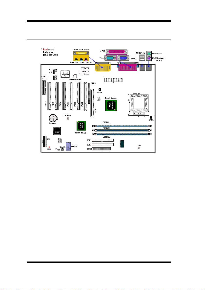
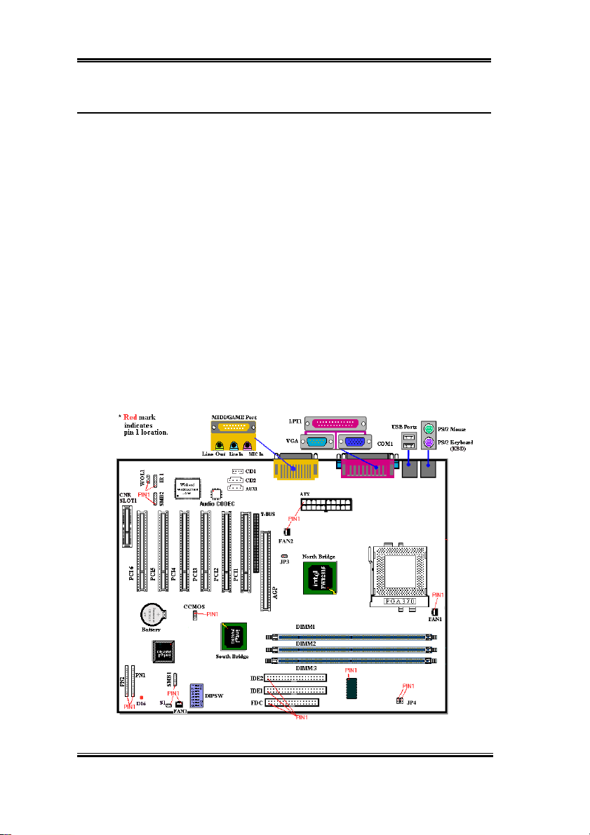
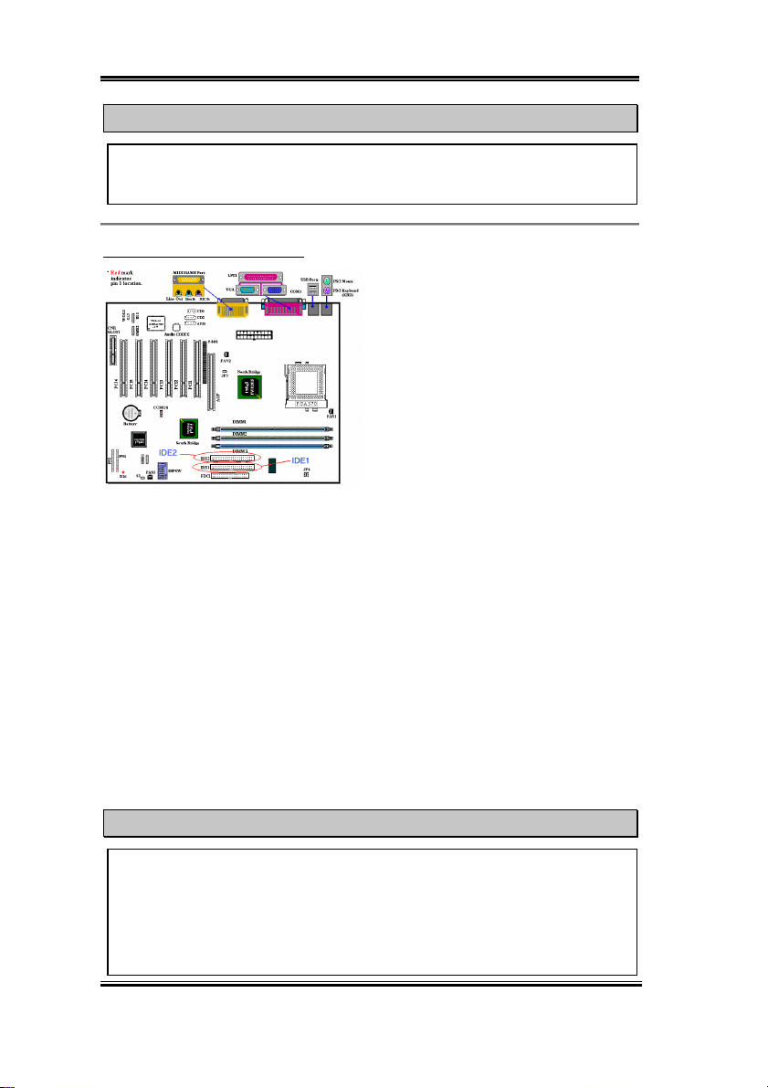
1-3. Layout Diagram
SL6
Figure 1-2. SL6 Motherboard component location
Page 9
Introduction of SL6 Features 1-5
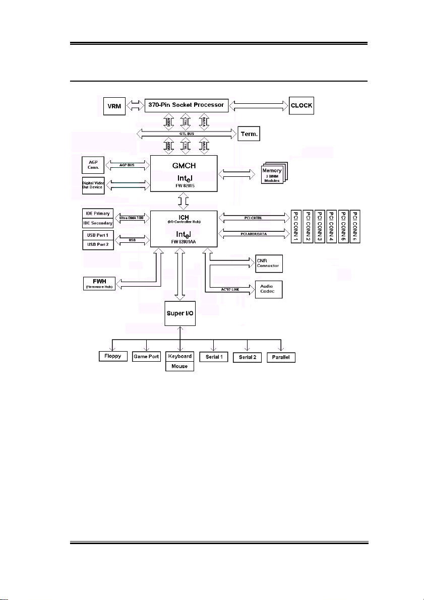
1-4. The System Block Diagram
Figure 1-3. System diagram of the INTEL 815 Chipset
User’s Manual
Page 10

1-6 Chapter1
SL6
Page 11

Installing the Motherboard 2-1
Chapter 2. Installing the Motherboard
This SL6 motherboard not only provides all standard equipment for classic personal
computers, but also provides great flexibility for meeting future upgrade demands. This
chapter will introduce step by step all of the standard equipment and will also present, as
completely as possible, future upgrade capabilities. This motherboard is able to support
Intel
Pentium III and Celeron processors now on the market. (For details, see
specifications in Chapter 1.)
This chapter is organized according the following features:
2-1 Installing the Motherboard to the Chassis
2-2 Installation of the Pentium
2-3 Installing System Memory
2-4 Connectors, Headers and Switches
$$$$
$$$$
$$$$$$$$
Before you install or unplug any connectors or add-on cards, please remember to turn the
ATX power supply switch off (fully turn the +5V standby power off), or disconnect the
power cord. Otherwise, you may cause the motherboard components or add-on cards to
malfunction or be damaged.
III / Celeron CPU
Before Proceeding with the Installation
$$$$
$$$$
$$$$$$$$
%%%%
User Friendly Instructions
Our objective is to enable the novice computer user to perform the installation by him or
herself. We have attempted to write this document in a very clear, concise and descriptive
manner to help overcome any obstacles you may face during installation. Please read our
instructions carefully and follow them step-by-step.
User’s Manual
Page 12

2-2 Chapter2
2-1. Installing the Motherboard to the Chassis
Most computer chassis will have a base on which there will be many mounting holes that
allows the motherboard to be securely attached and at the same time, prevents short circuits.
There are two ways to attach the motherboard to the base of chassis:
! with studs
! or with spacers
Please refer to figure 2-1, which shows the studs and spacers. There may be several types,
but all look similar to the figures below:
In principle, the best way to attach the
motherboard is with studs. Only if
you are unable to do this should you
attach the board with spacers. Take a
careful look at the motherboard and
you will see many mounting holes on
it. Line these holes up with the
mounting holes on the base. If the
holes line up and there are screw holes
this means you can attach the motherboard with studs. If the holes line up and there are only
slots, this means you can only attach the motherboard with spacers. Take the tip of the
spacers and insert them into the slots. After doing this to all the slots, you can slide the
motherboard into position aligned with the slots. After the motherboard has been positioned,
check to make sure everything is OK before putting the casing back on.
Figure 2-2 shows you the way to affix the motherboard using studs or spacers:
SL6
Page 13

Installing the Motherboard 2-3
Note
If the motherboard has mounting holes, but they don’t line up with the holes on the base
and there are no slots to attach the spacers, do not despair, you can still attach the
spacers to the mounting holes. Just cut the bottom portion of the spacers (the spacers
may be a little hard to cut , so mind your fingers). In this way, you can still attach the
motherboard to the base without worrying about short circuits. Sometimes you may
need to use the plastic springs to isolate the screw from the motherboard PCB surface as
the circuit wire may be too near the hole. Be careful. Do not let the screw contact the
printed circuit wire or parts on the PCB that are near the fixing hole. Otherwise it may
damage the board or cause board malfunctioning.
2-2. Installation of the Pentium
III CPU
The installation method for the CPU is printed on the package of the retention mechanism
that comes with the motherboard. You can refer to it while you install the CPU.
Note:
! Installing a heat sink and cooling fan is necessary for proper heat dissipation from
your CPU. Failing to install these items may result in overheating and damage of
your CPU.
! Please refer to your boxed processor installation or other documentation attached
with your CPU for detailed installing instructions.
User’s Manual
Page 14
2-4 Chapter2
2-3. Installing System Memory
This motherboard provides three 168-pin DIMM sites for memory expansion. The DIMM
sockets support 8Mx64 (64MB), 16Mx64 (128MB), 32Mx64 and (256MB) DIMM
modules. Minimum memory size is 64MB and maximum memory size is 512MB SDRAM.
In order to create a memory array, certain rules must be followed. The following set of rules
allows for optimum configurations.
! The memory array is 64 or 72 bits wide. (depending on with or without parity)
! Those modules can be populated in any order.
! Supports single and double density DIMMS.
Table 2-1. Valid Memory Configurations
Bank Memory Module Total Memory
Bank 0, 1
(DIMM1)
Bank 2, 3
(DIMM2)
Bank 4, 5
(DIMM3)
Total System Memory
8MB, 16MB, 32MB,
64MB, 128MB
8MB, 16MB, 32MB,
64MB, 128MB
8MB, 16MB, 32MB,
64MB, 128MB
8MB ~ 512MB
8MB ~ 512MB
8MB ~ 512MB
8MB ~ 512MB
Generally, installing SDRAM modules to your motherboard is an easy thing to do. You can
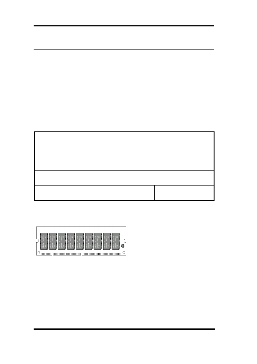
refer to figure 2-3 to see what a 168-pin PC100 & PC133 SDRAM module looks like.
DIMMs may be "snapped" directly into
the socket. Note: Certain DIMM sockets
have minor physical differences. If your
module doesn't seem to fit, please do not
Figure 2-3 PC100/PC133/VCM Module and
Component Mark
The following procedure will show you how to install a DIMM module into a DIMM socket.
Step 1. Before you install the memory module, please place the computer power switch in
the off position and disconnect the AC power cord.
Step 2. Remove the computer’s chassis cover.
SL6
force it into the socket as you may
damaged your memory module or
DIMM socket.
Page 15
Installing the Motherboard 2-5
Step 3. Before touching any electronic
components, make sure you first touch
an unpainted, grounded metal object to
discharge any static electricity stored on
your clothing or body.
Step 4. Locate your computer’s 168-pin
memory expansion DIMM socket.
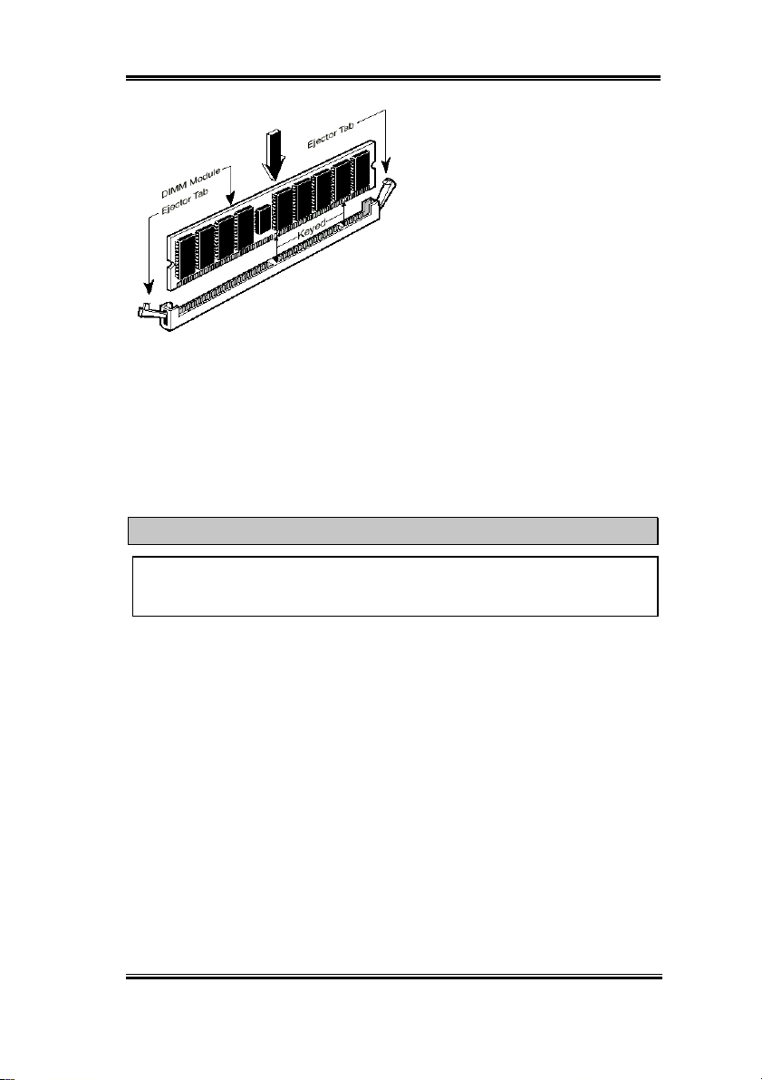
Step 5. Insert the DIMM module into
the expansion socket as shown in the
Figure 2-4. Memory module installation
figure 2-4 for the details. This insures the DIMM module will be plugged into the
socket in one way only. Firmly press the DIMM module into the DIMM socket,
making certain the module is completely seated in the DIMM socket.
Step 6. Once the DIMM module has been installed, the installation is complete and the
computer’s cover can be replaced. Or you can continue to install other devices and
add-on cards that are mentioned in the following section.
When you install a DIMM module fully into the DIMM socket, the eject tab should be
locked into the DIMM module very firmly and fit into its indention on both sides.
illustration. Note how the module is
keyed to the socket. You can refer to
Note
It is difficult to differentiate between the PC100, PC133 SDRAM and VCM DRAM
modules from the exterior. The only way to identify them is through the sticker on the RAM
module.
User’s Manual
Page 16
2-6 Chapter2
2-4. Connectors, Headers and Switches
Inside the case of any computer several cables and plugs have to be connected. These cables
and plugs are usually connected one-by-one to connectors located on the motherboard. You
need to carefully pay attention to any connection orientation the cables may have and, if any,
notice the position of the first pin of the connector. In the explanations that follow, we will
describe the significance of the first pin.
We will show you all of the connectors, headers and switches here, and tell you how to
connect them. Please pay attention and read the entire section for necessary information
before attempting to finish all of the hardware installation inside the computer chassis.
Figure 2-5 shows you all of the connectors and headers that we’ll discuss in the next section,
you can use this diagram to visually locate each connector and header we describe.
All connectors, headers and switches mentioned here will depend upon your system
configuration. Some features you may (or may not) have and need to connect or configure
depending on the peripheral. If your system doesn't have such add-on cards or switches you
can ignore some special feature connectors.
SL6
Figure 2-5. All Connectors and Headers for the SL6
Page 17
Installing the Motherboard 2-7
First, Let’s look at the headers that the SL6 uses, and what their functions are.
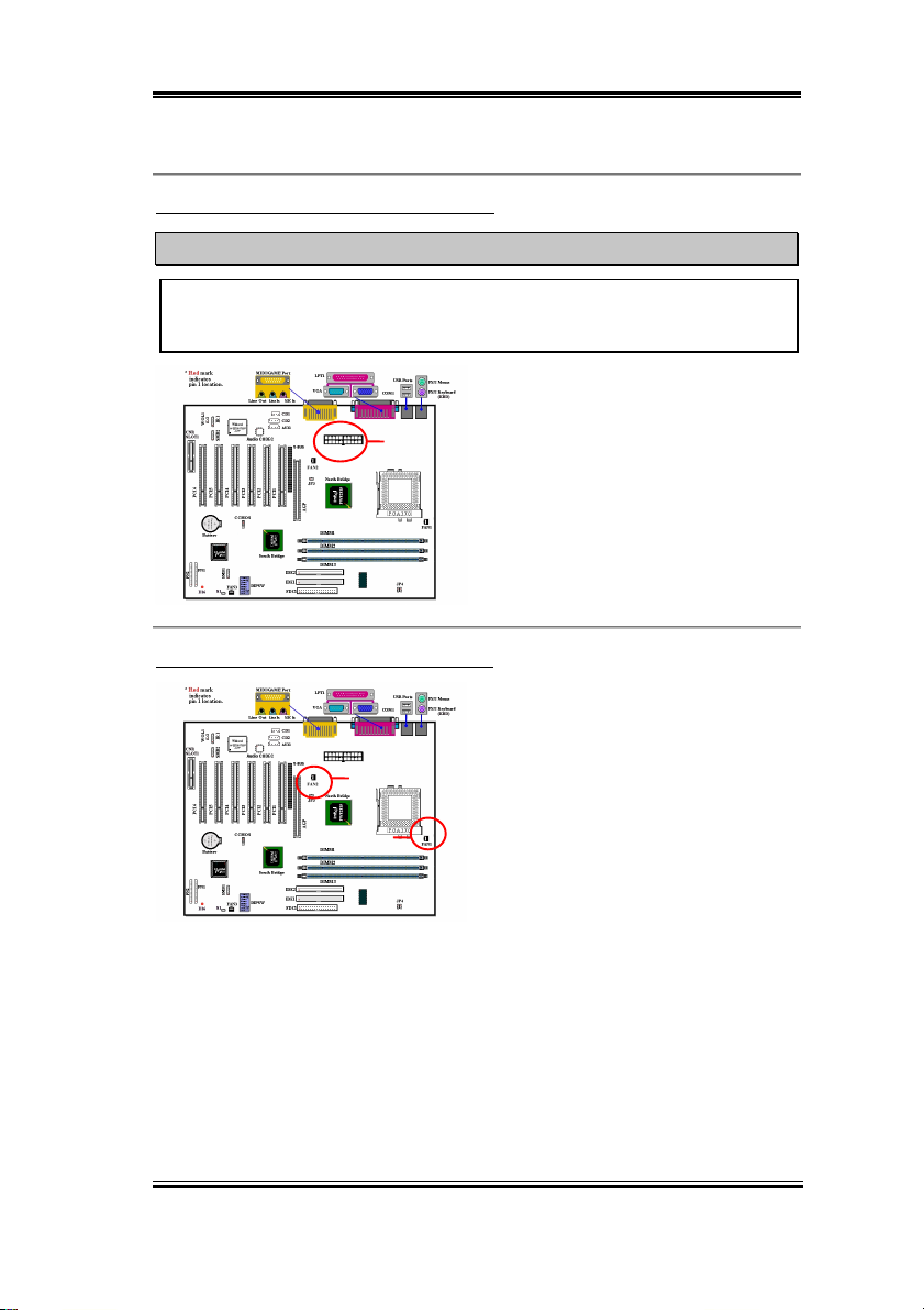
(1) ATXPWR1: ATX Power Input Connector
Caution
If the power supply connectors are not properly attached to the ATXPR1 power supply,
the power supply or add-on cards may be damaged.
Attach the connector from the power supply
to the ATXPR1 connector here. Remember
ATXP R1
(2 A ) /(2B ) / (2C): FA N1, FA N2 & FA N3 hea d er
FAN 2
FAN 1
you have to push the connector from the
ATX power supply firmly into the ATXPR1
connector, ensuring that you have a good
connection.
Note: Watch the pin position and the
orientation
Attach the connector from the individual
CPU fan to the header named FAN1. The
connector from the chassis fan should be
attached to the header FAN3 and the
connector from the power fan to FAN2.
You must attach the CPU fan to the
processor or your processor will work
abnormally or may be damaged by
overheating. To keep the computer’s
internal temperature steady and not too high,
connecting the chassis fan is imperative.
Note: Watch the pin position and the orientation
User’s Manual
Page 18
2-8 Chapter2
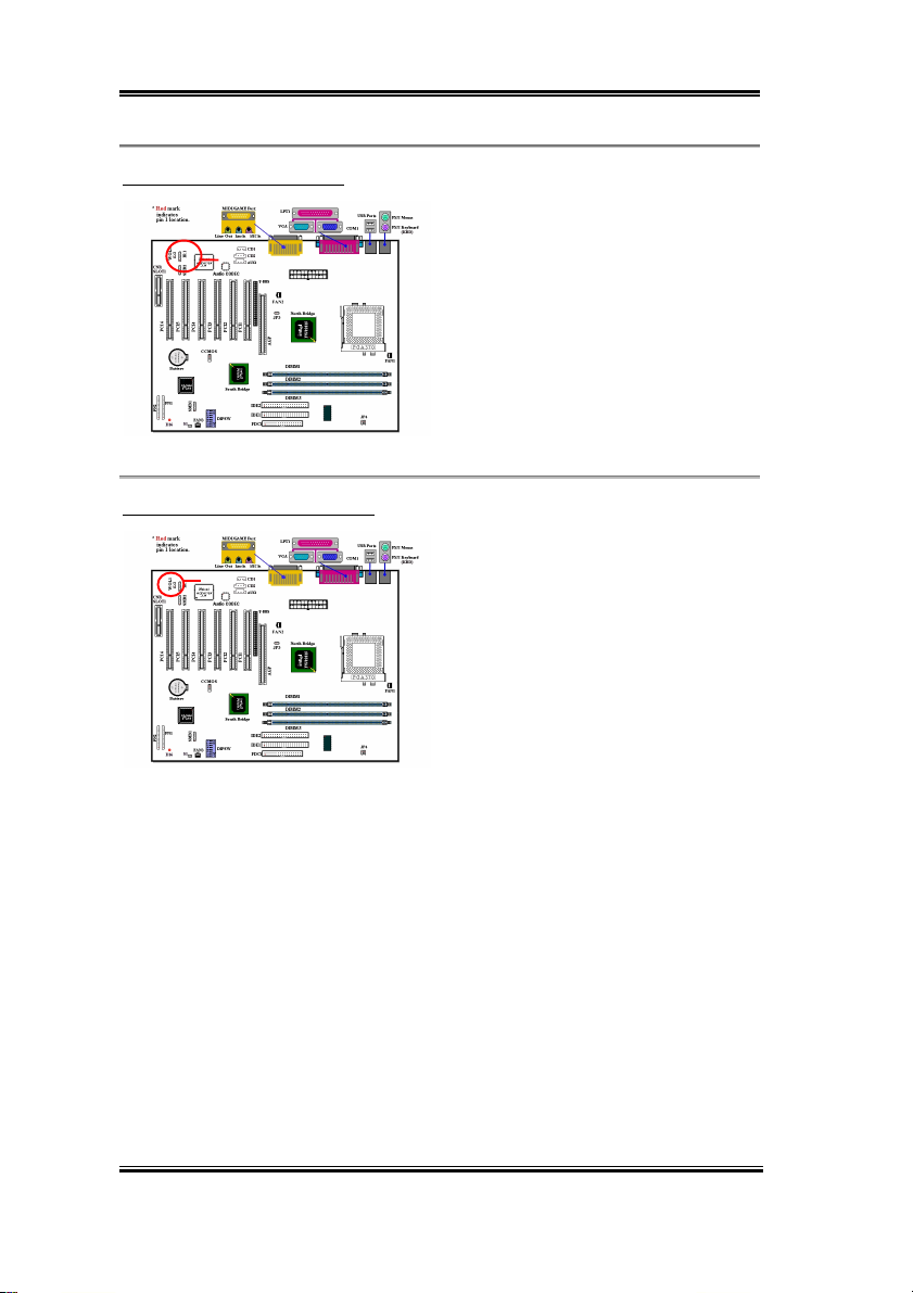
(3) IR1: IR Header (Infrared)
There is a specific orientation for pins 1
IR1
(4) WOL1: Wake on LAN Header
WOL1
through 5, attach the connector from the IR
KIT or IR device to the IR1 header (left row
only). This motherboard supports standard
IR transfer rates.
Note: Watch the pin position and the
orientation
If you have a network adapter that supports
this feature, then you can connect the
specific cable from the network adapter to
this header. This feature lets you wake up
your computer via remote control through a
local area network. You may need a specific
utility to control the wake up event, such as
the PCnet Magic Packet utility or other
similar utilities.
Note: Watch the pin position and the orientation
SL6
Page 19
Installing the Motherboard 2-9
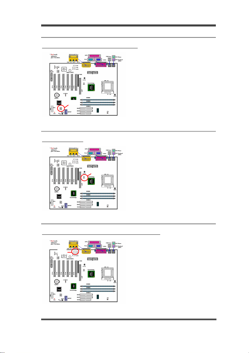
(5) SMB1: System Management Bus Connector
This connector is reserved for system
management bus (SM bus). The SM bus is a
specific implementation of an I
2
C bus. I2C is
a multi-master bus, which means that
multiple chips can be connected to the same
bus and each one can act as a master by
SMB1
initiating a data transfer. If more than one
master simultaneously tries to control the
bus, an arbitration procedure decides which
master gets priority.
Note: Watch the pin position and the orientation
(6) RT2 Thermister:
The RT2 is a thermistor used to detect the
system environmental temperature. It may
also be called a system temperature detector.
RT2
You can attach one end of the two-threaded
thermal cable that comes with the
motherboard to the RT2 header, then tape
the other end of the thermal cable on the
CPU’s heat sink. Generally speaking, the
location you tape the thermistor should be as
near the CPU chipset as possible and avoid having it near the CPU fan.
(7) CDIN1: Internal CD-ROM Drive Audio Cable Header
This header is for the internal CD-ROM
CD1
drive audio cable connection. Please check
your audio cable attached with the CD-
ROM drive to see which type of connector
you have and then plug it into this header.
User’s Manual
Page 20
2-10 Chapter2
(8) DIPSW: Front Side Bus Speed Setting DIP Switch
This switch allows you to manually setting
the front side bus speed.
(1) SW1 - SW2 on, SW3 - SW4 off: This is
to use the CPU default value (66 / 100 /
133MHz).
DIPSW
(3) SW5 on, SW6 off: This is the default setting.
(4) SW7: This is to enable or disable the On Board Codec. Set on to disable.
(5) SW8: This is to set the SoftMenu or None SoftMenu. Set on to None SoftMenu.
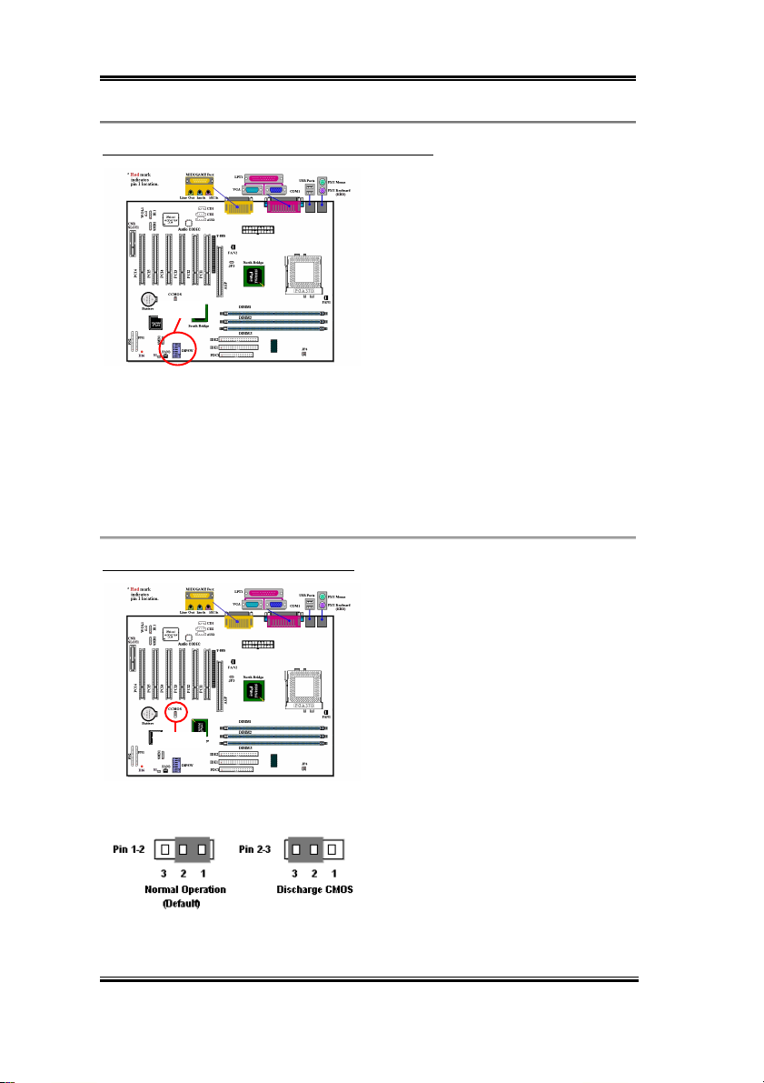
(9) CCMOS1: CMOS Discharge Jumper
(2) SW1 - SW2 off, SW8 on: This enables
you to adjust CPU clock manually by SW3 -
SW4.
SW3 - SW4 on: 66MHz
SW3 off, SW4 on: 100MHz
SW3 - SW4 off: 133MHz
CCMOS
Figure 2-6. CCMOS1 jumper setting
SL6
The jumper CCMOS discharges CMOS
memory. When you install the motherboard,
make sure this jumper is set for normal
operation (pin 1 and 2 shorted). See figure
2-6.
Page 21
Installing the Motherboard 2-11
Note
Before you clear the CMOS, you have to first turn the power off (including the +5V
standby power). Otherwise, your system may work abnormally or malfunction.
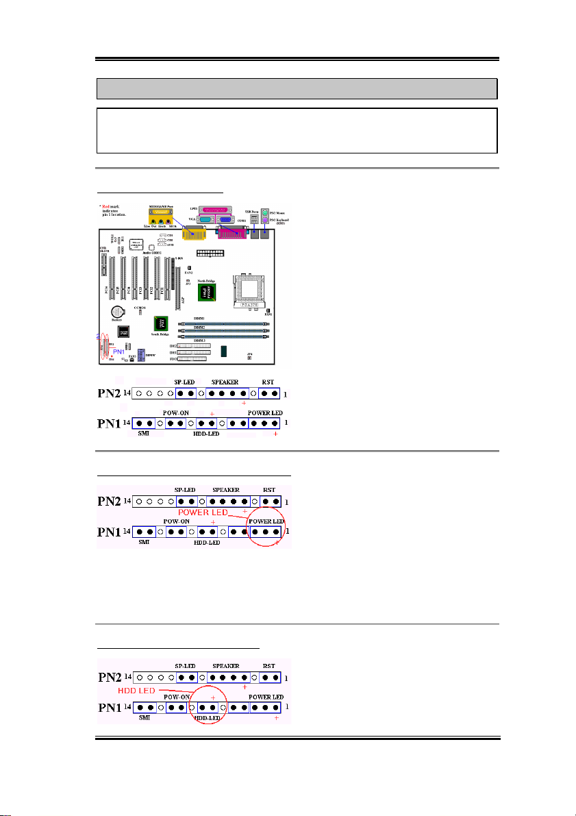
(10) PN1 and PN2 Headers
PN1 and PN2 are for switches and indicators
of the chassis’ front panel. There are several
functions that come from these two headers.
You have to watch the pin position and the
orientation, or you may cause system
malfunctions. Figure 2-7 shows you the
functions of PN1 and PN2.
Figure 2-7. The definition of PN1 and
PN2 pins
PN1 (Pin 1-2-3-4-5): Power LED Headers
There is a specific orientation for pins 1
through 3. Insert the three-threaded power
LED cable to pins 1~3. Check to make sure
the correct pins go to the correct connectors
on the motherboard. If you install them in the wrong direction, the power LED light will not
illuminate correctly.
Note: Watch the power LED pin position and orientation.
PN1 (Pin 7 - 8): HDD LED Header
Attach the cable from the case’s front panel
HDD LED to this header. If you install it in
the wrong direction, the LED light will not
illuminate correctly.
User’s Manual
Page 22
2-12 Chapter2
Note: Watch the HDD LED pin position and the orientation.
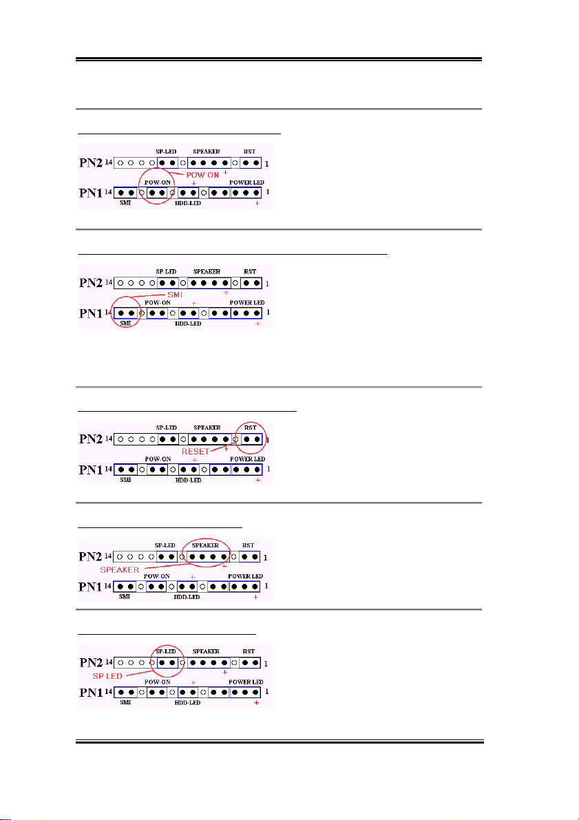
PN1 (Pin 10 - 11): Power on Switch Header
Attach the cable from the case’s front panel
power switch to this header.
PN1 (Pin 13-14): Hardware Suspend Switch (SMI Switch) Header
Attach the cable from the case’s front panel
suspend switch (if there is one) to this
header. Use this switch to enable/disable the
power management function through
hardware.
Note: If the ACPI function in the BIOS setup is enabled, this function will not work.
PN2 (Pin 1-2): Hardware Reset Switch Header
Attach the cable from the case’s front panel
reset switch to this header. Press and hold
the reset button for at least one second to
reset the system.
PN2 (Pin 4-5-6-7): Speaker Header
Attach the cable from the system speaker to
this header.
PN2 (Pin 9-10): Suspend LED Header
Insert the two-threaded suspend LED cable
into pin 9 and pin 10. If you install it in the
wrong direction, the LED light will not
illuminate correctly.
Note: Watch the Suspend LED pin position and the orientation.
SL6
Page 23
Installing the Motherboard 2-13
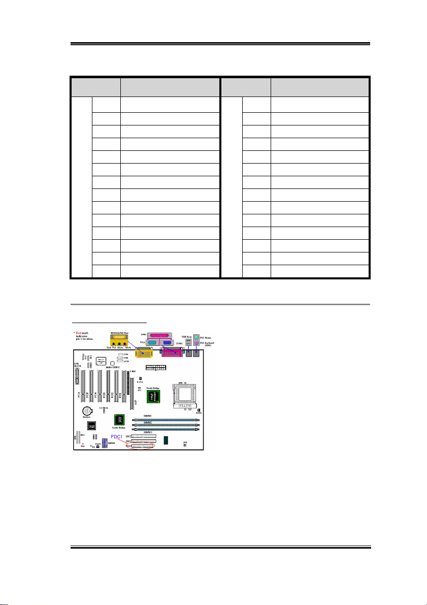
Table 2-3. PN1 and PN2 pin count name list
PIN Name Significance of signal PIN Name Significance of signal
PIN 1 +5VDC PIN 1 Ground
PIN 2 No connection PIN 2 Reset input
PIN 3 Ground PIN 3 Empty Pin
PIN 4 No Connection PIN 4 No Connection
PIN 5 No Connection PIN 5 +5 VDC
PN1
PIN6 Empty Pin PIN6 Ground
PIN 7 LED Power PIN 7 Ground
PIN 8 HDD active PIN 8 Empty Pin
PIN 9 Empty Pin PIN 9 Speaker Data
PIN 10 Ground PIN 10 No Connection
PIN 11 Power On/Off PIN 11 Empty Pin
PIN 12 Empty Pin PIN 12 No connection
PIN 13 Ground PIN 13 No connection
PIN 14 Suspend signal
Let’s now see the I/O connectors that the SL6 uses, and what their functions are.
(11) FDC1 Connector
PN2
PIN 14 No connection
This 34-pin connector is called the “floppy
disk drive connector”. You can connect a
360K, 5.25”, 1.2M, 5.25”, 720K, 3.5’’,
1.44M, 3.5” or 2.88M, 3.5” floppy disk
drive. You can even connect a 3 Mode
floppy disk drive (a 3 1/2” drive used in
Japanese computer systems).
A floppy disk drive ribbon cable has 34
wires and two connectors to provide the
connection of two floppy disk drives. After
connecting the single end to the FDC1, connect the two connectors on the other end to the
floppy disk drives. In general, people only install one floppy disk drive on their computer
system. The end attached to the longer length of ribbon should be attached to the
motherboard connector.
User’s Manual
Page 24
2-14 Chapter2
Note
A red mark on a wire typically designates the location of pin 1. You need to align pin 1
of the wire to pin 1 of the FDC1 connector and then insert.
(12) IDE1 and IDE2 Connectors
An IDE hard disk drive ribbon cable has 40
wires and two connectors to provide a
connection for two IDE hard disk drives.
After connecting the single end to the IDE1
(or IDE2), connect the two connectors on
the other end to the IDE hard disk drives (or
CD-ROM drive, LS-120, etc.). Again the
connector attached to the longer ribbon
length should be attached to the mobo.
Before you install a hard disk, there are
some things you need to be aware of:
“Primary” refers to the first connector on the motherboard; that is, the IDE1 connector on
♦
the motherboard.
“Secondary” refers to the second connector on the motherboard; that is, the IDE2
♦
connector on the motherboard.
Two hard disks can be connected to each connector:
♦
The first HDD is referred to as the “Master” and the second HDD is referred to as the
“Slave”.
For performance issues, we strongly suggest you don’t install a CD-ROM drive on the
♦
same IDE channel as a hard disk. Otherwise, the system performance on this channel may
drop. (how much depends on your CD-ROM drive performance)
Note
!The Master or Slave status of the hard disk drive is set on the hard disk itself. Please
refer to the hard disk drive user’s manual.
!A red mark on a wire typically designates the location of pin 1. You need to align the
wire pin 1 to the FDC1 connector pin 1, then insert the wire connector into the FDC1
connector.
SL6
Page 25
Installing the Motherboard 2-15
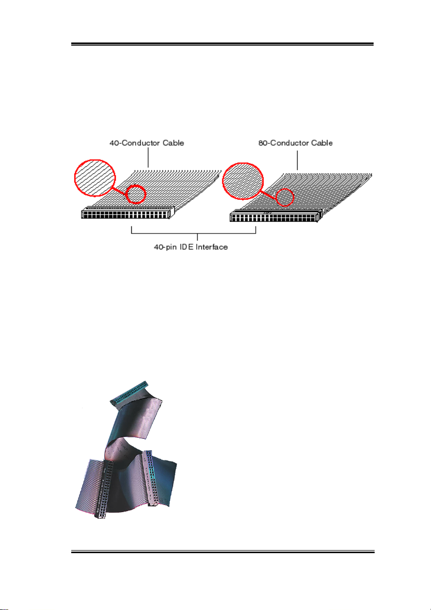
The SL6 supports the Ultra ATA/66 (Also known as Ultra DMA/66) specification. It
enhances existing Ultra ATA/33 technology by increasing both performance and data
integrity. This new high-speed interface doubles the Ultra ATA/33 burst data transfer rate to
66.6 Mbytes/sec. The result is maximum disc performance using the current PCI local bus
environment. Figure 2-8 shows you the different between the Ultra ATA/33 and Ultra
ATA/66 Conductor Cable.
Figure 2-8. The difference between Ultra ATA/33 and Ultra ATA/66 Conductor Cables
Figure 2-9 shows you a photo of an Ultra ATA/66 Conductor Cable. An Ultra ATA/66-
capable cable is a 40-pin, 80-conductor cable with a black connector on one end, a blue
connector on the other end and a gray connector in the middle. In addition, line 34 on the
cable should be notched or cut (this may be difficult to see).
Ultra ATA/66 is backwards compatible with all Ultra ATA/33 systems, but it will be limited
in its transfer mode to the Ultra ATA/33 (Ultra DMA Mode 2 - 33 Mbytes/sec) or PIO Mode
4 (16.6 Mbytes/sec). Ultra ATA/66 hard drives are 100 percent backward compatible with
both Ultra ATA/33 and DMA and with existing ATA
(IDE) hard drives, CD-ROM drives, and host systems.
The Ultra ATA/66 protocol and commands are designed
to be compatible with existing ATA (IDE) devices and
systems. Although a new 40-pin, 80-conductor cable is
required for Ultra ATA/66, the chip set pin connector
remains the same at 40. Hard drives that support Ultra
ATA/66 also support Ultra ATA/33 and legacy ATA (IDE)
specifications.
There are four requirements for attaining Ultra ATA/66:
*The drive must support Ultra ATA/66.
Figure 2-9. Photo of an Ultra
ATA/66 Conductor Cable
*The motherboard and system BIOS (or an add-in
controller) must support Ultra ATA/66.
User’s Manual
Page 26
2-16 Chapter2
*The operating system must support Direct Memory Access (DMA); Microsoft Windows
98 and Windows 95B (OSR2) support DMA.
*The cable must be an 80-pin conductor. The length should not exceed 18 inches. If all of
the above requirements are met, you can enjoy the Ultra ATA/66 features of your computer
system.
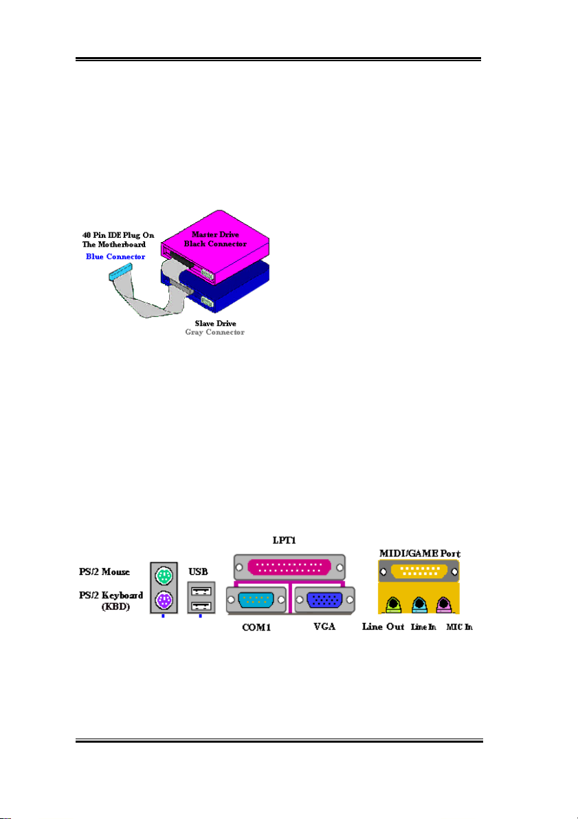
How to install the Ultra ATA/66 Cable Assembly:
& The BLUE connector MUST be plugged
into the motherboard or your system will not
work.
& Each connector on the Ultra ATA/66
cable assembly has a small polarization tab
centrally located on the body of the plastic.
This fits into the matching slot on the mating
plugs on the motherboard and the drives,
Figure 2-10. How to connect an ATA/66
Cable to the Motherboard
& The red line on the cable should be aligned with pin #1. On the drives this will result in the
red line facing the power connector. Attach the BLUE connector to the appropriate 40 pin
IDE plug on the motherboard.
thus assuring positive mating (pin #1 to pin
#1)
& Attach the BLACK connector to the mating plug on the master hard drive. Attach the
GREY connector to the mating plug on the slave drive (secondary hard drive, CD ROM,
or tape drive). Please refer figure 2-10.
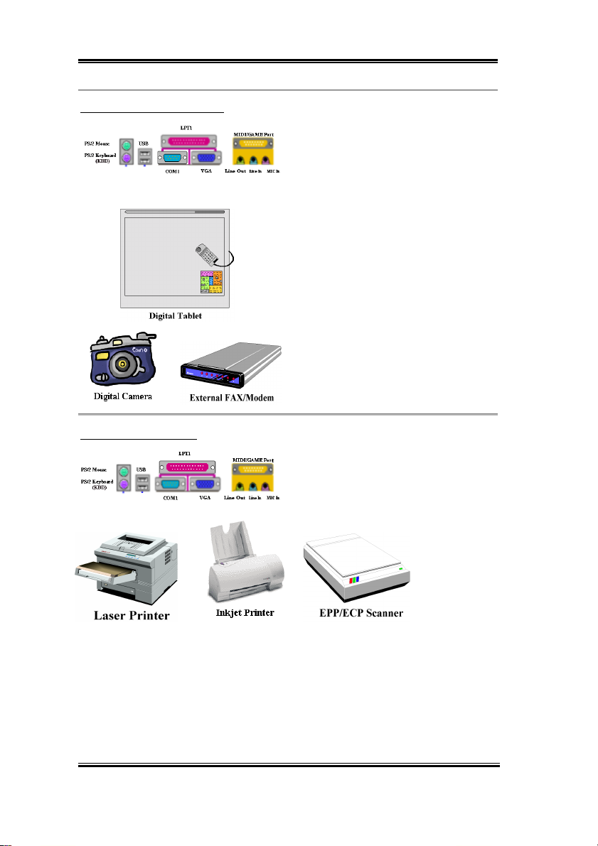
Figure 2-11. SL6 back panel connectors
Figure 2-11 shows the SL6 back panel connectors. These connectors are for connection to
outside devices to the motherboard. We will describe which devices will attach to these
connectors below.
SL6
Page 27
Installing the Motherboard 2-17
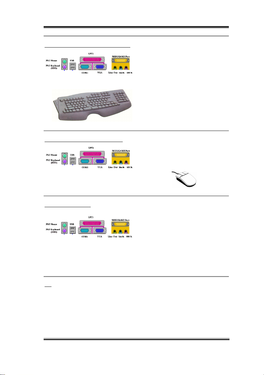
KM1 Lower: PS/2 Keyboard Connector
Attach a PS/2 keyboard connector to this
6-pin Din-connector. If you use an AT
keyboard, you can go to a computer store to
purchase an AT to ATX converter adapter.
You can then connect your AT keyboard to
this connector. We suggest you use a PS/2
keyboard for best compatibility.
KM1 Upper: PS/2 Mouse Connector
Attach a PS/2 mouse to this 6-pin Din-
connector.
USB Port Connectors
This motherboard provides two USB ports.
Attach the USB connector from the
individual device to these connectors.
You can attach USB devices such as a scanner, digital speakers, monitor, mouse, keyboard,
hub, digital camera, joystick etc. to one of each of the USB connectors. You must make sure
your operating system supports this feature and you may need to install an additional driver
for individual devices. Please refer to your device user’s manual for detailed information.
User’s Manual
Page 28
2-18 Chapter2
Serial Port COM1 Connector
This motherboard provides one COM port.
You can connect an external modem, mouse
or other devices that support this
communication protocol to this connector.
You can decide which external device you
want to connect to COM1. The COM port
can only have one device connected at a
time.
Parallel Port Connector
This parallel port is also called an “LPT”
port because it usually connects to the
printer. You can connect other devices that
support this communication protocol, like
an EPP/ECP
scanner, etc.
SL6
Page 29
Installing the Motherboard 2-19
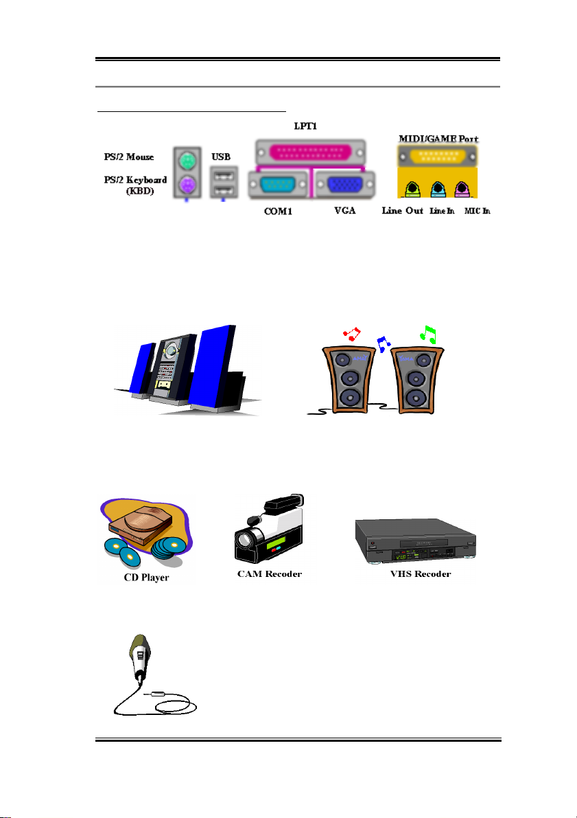
Line Out, Line In and Mic In Connector
Line Out connector:You can connect an external stereo speaker signal input plug to this
connector, or you can connect the plug from here to the stereo audio equipment AUX signal
input socket. Remember, the motherboard does not have a built in amplifier to drive the
speaker. You must use a speaker that has a built in amplifier. Otherwise, you may not be able
to hear any sound or only a small volume of sound from the speaker.
Line In Connector: You can connect the TV adapter audio output signal, or external
audio sources, like a CD walkman, video camcorder, VHS recorder audio output signal plug
to this connector. Your audio software can control the input level for the line-in signal.
Mic In Connector: You can connect the plug from the microphone to this connector. Do
not connect other audio (or signal) sources to this connector.
User’s Manual
Page 30
2-20 Chapter2
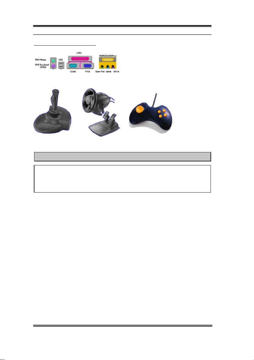
MIDI/GAME Port Connector
You can connect your joystick, game pad,
or other simulation hardware device DIN
15-pin plugs to this connector. Please refer
to the further connection notes of the
device’s user's manual for further detailed
information.
Note
This chapter contains many color drawing diagram and photos, we strongly recommend
you to read this chapter using the PDF file that is included on the CD. It will provide you
with greater clarity.
SL6
Page 31

BIOS Setup 3-1
Chapter 3. Introducing the BIOS
The BIOS is a program located on a Flash Memory chip on the motherboard. This program
will not be lost when you turn the computer off. This program is also referred to as the boot
program. It is the only channel the hardware circuit has to communicate with the operating
system. Its main function is to manage the setup of the motherboard and interface card
parameters, including simple parameters such as time, date, hard disk drive, as well as more
complex parameters such as hardware synchronization, device operating mode, CPU SOFT
MENU™ II features and setup of CPU speed. The computer will operate normally, or will
operate at its best, only if all of these parameters are correctly configured through the BIOS.
Don’t change the parameters inside the BIOS unless you fully understand
''''
their meanings and consequences
The parameters inside the BIOS are used to setup the hardware synchronization or the
device-operating mode. If the parameters are not correct, they will produce errors, the
computer will crash, and sometimes you will not even be able to boot the computer after
it has crashed. We recommend that you do not change the parameters inside the BIOS
unless you are very familiar with them. If you are not able to boot your computer
anymore, please refer to the section “Erase CMOS data” in Chapter 2.
When you start the computer, the BIOS program controls it. The BIOS first operates an
auto-diagnostic test called POST (Power On Self Test) for all of the necessary hardware. It
then configures the parameters of the hardware synchronization, and detects all of the
hardware. Only when these tasks are completed does it give up control of the computer to
the next level, which is the operating system (OS). Since the BIOS is the only channel for
hardware and software to communicate, it is the key factor for system stability, and in
ensuring that your system performs at its best. After the BIOS has achieved the auto-
diagnostic and auto-detection operations, it will display the following message:
PRESS DEL TO ENTER SETUP
The message will be displayed for three to five seconds, if you press the Del key, you will
access the BIOS Setup menu. At that moment, the BIOS will display the following message:
User’s Manual
Page 32

3-2 Chapter3
Figure 3-1. CMOS Setup Utility
In the BIOS Setup main menu of Figure 3-1, you can see several options. We will explain
these options step by step in the following pages of this chapter, but let us first see a short
description of the function keys you may use here:
! Press Esc to quit the BIOS Setup.
↑↓←→
! Press
to confirm or to modify.
! Press F10 when you have completed the setup of BIOS parameters to save these
parameters and to exit the BIOS Setup menu.
! Press Page Up/Page Down or +/- keys when you want to modify the BIOS parameters for
the active option.
SL6
(up, down, left, right) to choose, in the main menu, the option you want
Page 33

BIOS Setup 3-3
Computer Knowledge: CMOS Data
Maybe you have heard somebody saying that his or her CMOS DATA was lost. What is
the CMOS? Is it important? The CMOS is the memory used to store the BIOS
parameters that you have configured. This memory is passive. You can read its data, and
you can also store data in it. But this memory has to be powered by a battery in order to
avoid any loss of its data when the computer is turned off. Since you may have to
change the CMOS battery when it is out of power, and if doing so you will lose all
CMOS data, we recommend that you write down all the parameters of your hardware,
or to put a label with these parameters on your hard disk.
User’s Manual
Page 34

3-4 Chapter3
3-1. CPU Setup [SOFT MENU™ II]
™
The CPU can be setup through a programmable switch (CPU SOFT MENU
replaces the traditional manual hardware configuration. This feature allows the user to more
easily complete the installation procedures. You can install the CPU without configuring any
jumpers or switches. The CPU must be setup according to its specifications.
You can press <F1> at any time for help.
II), that
Figure 3-2. CPU SOFT MENU
™
II
CPU Name Is:
➤ Intel Celeron
MMX
➤ Intel Pentium III MMX
CPU Operating Speed:
This option sets the CPU speed. In this field, the CPU speed is indicated like this: CPU
speed = External clock * Multiplier factor, select the CPU speed according the type and the
speed of your CPU. For Intel Pentium® III and Celeron™ MMX processors, you can choose
the following settings:
SL6
Page 35

BIOS Setup 3-5
➤300 (66) ➤333 (66) ➤366 (66) ➤400 (66) ➤433 (66)
➤466(66) ➤500 (66) ➤500 (100) ➤533 (66) ➤550 (100)
➤500 (100) ➤533 (66) ➤550 (100) ➤566 (66) ➤600 (66)
➤600 (100) ➤600 (133) ➤633 (66) ➤650 (100) ➤667 (133)
➤700 (100) ➤733 (133) ➤750 (100) ➤800 (100) ➤800 (133)
➤800 (133) ➤850 (100) ➤866 (133) ➤933 (133) ➤1G
➤User Define
User defined external clock and multiplier factor:
➤➤➤➤ User Defined
$$$$
$$$$
$$$$$$$$
The wrong settings of the multiplier and external clock in certain circumstances may
cause CPU damage. Setting the working frequency higher than the PCI chipset or
processor specs, may cause abnormal memory module functioning, system hangs, hard
disk drive data lose, abnormal functioning of the VGA card, or abnormal functioning
with other add-on cards. Using non-specification settings for your CPU is not the
intention of this explanation. These should be used for engineering testing, not for
normal applications.
If you use non-specification settings for normal operation, your system may not be
stable, and may effect system reliability. Also, we do not guarantee the stability and
compatibility for settings that are not within specification, and any damage of any
elements on the motherboard or peripherals, is not our responsibility.
Ext. Clock (PCI):
✏
➤66MHz (2:3:1) (((( default ➤100MHz(3:3:1) ➤133MHz (4:3:1)
➤68MHz (2:3:1)* ➤70MHz (2:3:1)* ➤72MHz (2:3:1)*
➤75MHz (2:3:1)* ➤77MHz (2:3:1)* ➤83MHz (3:3:1)*
➤90MHz (3:3:1)* ➤103MHz (3:3:1)* ➤112MHz (3:3:1)*
➤115MHz (3:3:1)* ➤120MHz (3:3:1)* ➤125MHz (4:3:1)*
➤125MHz (3:3:1)* ➤128MHz (4:4:1)* ➤130MHz (4:3:1)*
➤130MHz (4:4:1)* ➤133MHz (4:4:1)* ➤137MHz (4:3:1)*
➤137MHz (4:4:1)* ➤140MHz (4:3:1)* ➤140MHz (4:4:1)*
➤145MHz (4:3:1)* ➤145MHz (4:4:1)* ➤150MHz (4:3:1)*
➤150MHz (4:4:1)* ➤153MHz (4:3:1)* ➤153MHz (4:4:1)*
War ni ng
$$$$
$$$$
$$$$$$$$
How is each component’s working frequency calculated? For starters, everything is
derived from the clock generator on the motherboard. Upon boot up the CPU will
give the clock generator the default value for the Front Side Bus (FSB). Once the
User’s Manual
Page 36

3-6 Chapter3
FSB has been set, all of the other components will be able derive their proper
operating frequencies.
For example: If you have a CPU rated for a 100MHz FSB, the operating frequencies
for the proper values for the FSB : SDRAM : PCI for your CPU would be
calculated thusly:
Pentium III
100MHz (3:3:1) (each divided by 3) (FSB) 100MHz : (SDRAM) 100MHz : (PCI)
33MHz
CPU FSB value = 100MHz x 1 = 100MHz (proper FSB value for this CPU)
SDRAM value = FSB 100MHz x 1 = 100MHz (proper value for PC100 RAM)
PCI value = FSB 100MHz x 1/3 = 33MHz (proper value for PCI bus)
So that for this example above you can see that the x1, x1, x 1/3 values in
relation to the FSB can be written as
Additionally, for the working value of the CPU (in this case a Pentium® III 500MHz
you calculate it like this:
CPU working value = FSB 100MHz x 5 = 500MHz (proper value for this CPU)
Also, the AGP value is derived from the PCI value so that:
®
CPU with 100MHz FSB running at 500MHz:
100MHz (1: 1: 1/3)
AGP value = PCI value (33MHz) x 2 or (4) = 66MHz or (132MHz) (proper
value for AGP bus) For a 2x AGP it works at double the speed of the PCI bus,
and four times for 4x AGP.
When the FSB is above 100MHz, such as 133MHz, you can choose a PCI divider of
4, again giving you the proper 33MHz value.
Now, in the BIOS they do not write dividers in fractions but rather in whole integers,
so that again for the 100MHz FSB example,
above it looks like this:
100MHz (3:3:1)
But you need to remember that each value is also divided by 3
you can look at it as if it were:
100MHz (3:3:1) each divided by 3
but you can also look at it as if it were:
SL6
100MHz (1: 1: 1/3)
,
in the table
Page 37

BIOS Setup 3-7
100MHz (1: 1: 1/3) each multiplied times 3 then (divided by 3)
or
100MHz (3/3: 3/3: 1/3) each multiplied times 3 then (divided by 3)
which both equal:
100MHz (3:3:1)
Now the final point about this table is that it does not show the necessary divider, i.e.
for the 100MHz (3:3:1) example you still need to divide each by 3, even though it
does not show that in the table.
Accordingly, for the 66MHz (2:3:1) you will divide each by 2 and for the 138MHz
(4:3:1) example you would divide each by 4. The first value in the parenthesis is the
value for the CPU’s FSB, and because everything derives its working frequency
from the FSB, that value must always equal 1. So for (3:3:1) you need to divide by 3,
for (2:3:1) you need to divide by 2 and for (4:3:1) you need to divide by 4.
So for the 100MHz (3:3:1) example in the table above, to get the working values you
are taking the (3:3:1) numbers and multiplying by 3 then dividing by 3.
For another example, in the table you have 138MHz (4:3:1) (divided by 4). You can
look at it like this: 138MHz (1: 3/4: 1/4). Each multiplied times 4 will give you the
same value as 138MHz (4:3:1). (needing to be divided by 4 again). So that for the
FSB you have 4 divided by 4 giving you a value of 1, so that 138MHz will come out
to 138MHz.
CPU FSB value =138MHz x1=138MHz (approximate proper FSB value for this
CPU)
SDRAM value = FSB 138MHz x 3/4 = 103.5MHz (approximate proper value
for PC100 RAM)
PCI value = FSB 138MHz x 1/4 = 34.5MHz (approximate proper value for PCI
bus)
(divided by 3)
Giving you all the proper values
(within a few MHz or so, its
never exactly precise)
Another way to look at it would be that for the 138MHz (4:3:1) example, you could
use this “maximum number” value of 4, and then you could divide FSB value of
138MHz by 4 which equals 34.5MHz. You could then use 34.5MHz as the base
number to be multiplied by the number for the components. So that:
User’s Manual
Page 38

3-8 Chapter3
CPU FSB frequency will be 34.5MHz x 4 =138MHz.
The SDRAM working frequency will be 34.5MHz x 3 =103.5MHz.
And the PCI bus working frequency will be 34.5MHz x 1 = 34.5MHz.
Giving you all the proper values
(within a few MHz or so, its
never exactly precise.)
ABIT patented technology, SoftMenu™ allows you to adjust the FSB working
frequency, when you adjust the working frequency, please choose the proper values
for the FSB : SDRAM : PCI for your CPU. For example:
A CPU rated for 66MHz FSB ( such as Celeron
66MHz (2:3:1) (each divided by 2): 66MHz : 100MHz : 33MHz
or a CPU rated for 100MHz FSB (such as Pentium
PGA)
100MHz (3:3:1) (each divided by 3) 100MHz : 100MHz : 33MHz
or a CPU rated for 133MHz FSB (such as a Pentium
FC-PGA)
133MHz (4:3:1) (each divided by 4) 133MHz : 100MHz : 33MHz
Note: the various components and their corresponding “bus speeds” should still
work fine, nonetheless going too far “out of spec” may cause system damage
or malfunction. System performance will depend mainly on the quality of the
components used.
Note
CPU bus speed above 66MHz/100MHz/133MHz supported but not guaranteed due to
the PCI and chipset specs.
™
)
®
III Coppermine using FC-
®
III Coppermine using
Multiplier Factor:
✏
You can choose from the following multiplier factors:
➤ 2.0 ➤ 2.5 ➤ 3.0 ➤ 3.5 ➤ 4.0 ➤ 4.5 ➤ 5.0 ➤ 5.5 ➤ 6.0
➤ 6.5 ➤ 7.0 ➤ 7.5 ➤ 8.0 ➤ 8.5 ➤ 9.0 ➤ 9.5 ➤10.0 ➤ 10.5
➤ 11.0
However, differences will exist because of the various brands and types available.
SL6
Page 39

BIOS Setup 3-9
Note
According to Celeron™ PPGA MMX processor types, some Celeron™ PPGA MMX
processors will have the multiplier factor locked and the signal disabled. In this
situation, there is no way to choose a higher multiplier factor.
Speed Error Hold:
✏
The default setting is “Disabled”. If you change the setting to “Enabled” when the
CPU speed setting is wrong, the system will hold.
Normally, we do not recommend that you use the “User Define” option to setup CPU
speed and multiplier factors. This option is for setup of future CPUs whose
specifications are still unknown. The specifications of all present CPUs are included
in the default settings. Unless you are very familiar with all CPU parameters, it is
very easy to make mistakes when you define the external clock and the multiplier
factor by yourself.
Solution in case of booting problem due to invalid clock setup:
Normally, if the CPU clock setup is wrong, you will not be able to boot. In this case, turn the
system off then on again. The CPU will automatically use its standard parameters to boot.
You can then enter the BIOS Setup again and set up the CPU clock. If you can’t enter the
BIOS setup, you must try turning the system on a few times (3~4 times) or press “INSERT”
when turning on, and the system will automatically use its standard parameters to boot. You
can then enter BIOS SETUP again and set up the new parameters.
When you change your CPU:
This motherboard has been designed in such a way that you can turn the system on after
having inserted a CPU in the socket without having to configure any jumpers or DIP
switches. If you change your CPU, normally you just have to turn off the power supply,
change the CPU and then set up the CPU parameters through SOFT MENU
™
II. However,
if the new CPU is slower than the old one (and is the same brand and type), we offer you two
methods to successfully complete the CPU change operation.
Method 1: Setup up the CPU for the lowest speed for its brand. Turn the power supply off
and change the CPU. Then turn the system on again, and set up the CPU
parameters through SOFT MENU
™
II.
Method 2: Since you have to open the computer case when you change the CPU, it could be
a good idea to use the CCMOS jumper to erase the parameters of the original
User’s Manual
Page 40

3-10 Chapter3
CPU and to enter BIOS Setup to set up CPU parameters again.
Attention
After setting up the parameters and leaving the BIOS SETUP, and having verified that
the system can be booted, do not press the Reset button or turn off the power supply.
Otherwise the BIOS will not read correctly, the parameters will fail and you must enter
SOFT MENU™ II again to set up the parameters all over again.
CPU Power Supply:
This option allows you to switch between CPU default and user-defined voltages.
➤➤➤➤CPU Default: The system will detect the CPU type and select the proper voltage
automatically. When it is enabled, the option “Core Voltage” will show
the current voltage setting that is defined by the CPU and this will not be
changeable. We recommend using this CPU default setting and not
changing it unless the current CPU type and voltage setting can not be
detected or is not correct.
➤➤➤➤User Define: This option lets the user select the voltage manually. You can change
values of the “Core Voltage” option lists by using the Page Up and Page
Down keys.
Spread Spectrum:
Two options are available: Disabled ) Enabled. The default setting is Disabled. For EMC
(Electro-Magnetic Compatibility) testing, you may need to adjust these options for optimal
results. We do not recommend you change the default, except for special reasons. Some
values you select may cause system instability under some situations. Please be careful.
SL6
Page 41

BIOS Setup 3-11
3-2. Standard CMOS Features Setup Menu
This section contains the basic configuration parameters of the BIOS. These parameters
include date, hour, VGA card, FDD and HDD settings.
Figure 3-3A. Standard CMOS Setup Screen Shot
Date (mm:dd:yy):
You can set the date in this item: month (mm), date (dd) and year (yy).
Time (hh:mm:ss):
You can set the time in this item: hour (hh), minute (mm) and second (ss).
IDE Primary Master / Slave and IDE Secondary Master / Slave:
These items have a sub-menu to let you choose further options. You can refer to figure 3-4 to
check what options are available.
User’s Manual
Page 42

3-12 Chapter3
Figure 3-3B. IDE Primary Master Setup Screen Shot
IDE HDD Auto-Detection:
Press the Enter key for the BIOS to auto detect all detailed parameters of the hard disk
drivers (HDD). If auto detection is successful, the correct values will be shown in the
remaining items of this menu.
Note
* A new IDE HDD must be first formatted, otherwise it can not read/write. The basic
step in using a HDD is to make a HDD low-level format, then run FDISK, and then
FORMAT the drive. Most current HDDs have already been subjected to low-level
format at the factory, so you can probably skip this operation. Remember though, the
primary IDE HDD must have its partition set to active within the FDISK procedure.
+ If you are using an old HDD that is already formatted, auto detection can not detect
the correct parameters. You may need to do a low-level format or set the parameters
manually, and then check if the HDD is working.
SL6
Page 43

BIOS Setup 3-13
IDE Primary Master:
Three settings are available: Auto, Manual and None. If you choose Auto, the BIOS will
automatically check what kind of hard disk you are using. If you want to set the HDD
parameters yourself, make sure you fully understand the meaning of the parameters, and be
sure to refer to the manual provided by the HDD manufacture to get the settings right.
Access Mode:
Since old operating systems were only able to support HDDs with capacities no bigger than
528MB, any hard disk with more than 528MB was unusable. AWARD BIOS features a
solution to this problem: you can, according to your operating system, choose four operating
modes: NORMAL ) LBA ) LARGE )Auto.
The HDD auto detection option in the sub-menu will automatically detect the parameters of
your hard disk and the mode supported.
➤➤➤➤ Auto:
Lets the BIOS detect your HDD access mode and make the decisions.
➤➤➤➤ Normal mode:
Standard normal mode supports hard disks of up to 528MB or less. This mode directly
uses positions indicated by Cylinders (CYLS), Heads, and Sectors to access data.
➤➤➤➤ LBA (Logical Block Addressing) mode:
The earlier LBA mode can support HDD capacities of up to 8.4GB, and this mode uses a
different method to calculate the position of disk data to be accessed. It translates
Cylinders (CYLS), Heads and Sectors into a logical address where data is located. The
Cylinders, Heads, and Sectors displayed in this menu do not reflect the actual structure
of the hard disk. They are just reference values used to calculate actual positions.
Currently, all high capacity hard disks support this mode and that is why we recommend
you use this mode. Currently, the BIOS can support the INT 13h extension function,
enabling the LBA mode to support hard disk drive capacities exceeding 8.4GB.
➤➤➤➤ Large Mode:
When the number of cylinders (CYLs) of the hard disk exceeds 1024 and DOS is not
able to support it, or if your operating system does not support LBA mode, you should
select this mode.
Capacity:
This item auto displays your HDD size. Note that this size is usually slightly greater than the
User’s Manual
Page 44

3-14 Chapter3
size given by a disk checking program of a formatted disk.
Note
All the items below are available when you set the item Primary IDE Master to Manual.
Cylinder:
When disks are placed directly above one another along the shaft, the circular vertical
"slice" consisting of all the tracks located in a particular position is called a cylinder. You
can set the number of cylinders for a HDD. The minimum number you can enter is 0, the
maximum number you can enter is 65536.
Head:
This is the tiny electromagnetic coil and metal pole used to create and read back the
magnetic patterns on the disk (also called the read/write head). You can configure the
number of read/write heads. The minimum number you can enter is 0, the maximum number
you can enter is 255.
Precomp:
The minimum number you can enter is 0, the maximum number you can enter is 65536.
War ni ng
Setting a value of 65536 means no hard disk exists.
Landing Zone:
This is a non-data area on the disk's inner cylinder where the heads can rest when the power
is turned off. The minimum number you can enter is 0, the maximum number you can enter
is 65536.
Sector:
The minimum segment of track length that can be assigned to stored data. Sectors usually
are grouped into blocks or logical blocks that function as the smallest units of data permit.
You can configure this item to sectors per track. The minimum number you can enter is 0,
the maximum number you can enter is 255.
Drive A & Drive B:
If you have installed the floppy disk drive here, then you can select the type of floppy drive
it can support. Six options are available: None)360K, 5.25 in. ) 1.2M, 5.25in. ) 720K,
3.5 in. ) 1.44M, 3.5 in. ) 2.88M, 3.5 in.
SL6
Page 45

BIOS Setup 3-15
Floppy 3 Mode Support:
Four options are available: Disabled ) Driver A ) Driver B ) Both. The default setting is
Disabled. 3 Mode floppy disk drives (FDD) are 3 1/2” drives used in Japanese computer
systems. If you need to access data stored in this kind of floppy, you must select this mode,
and of course you must have a 3 Mode floppy drive.
Video:
You can select the VGA modes for your video adapter, four options are available:
EGA/VGA ) CGA 40 ) CGA 80 ) MONO. The default setting is EGA/VGA.
Halt On:
You can select which type of error will cause the system to halt. Five options are available:
All Errors ) No Errors ) All, But Keyboard ) All, But Diskette ) All, But Disk/Key.
You can see your system memory list in the lower right box, it shows the Base Memory,
Extended Memory and total Memory size configurations in your system. It is detected by the
system during boot-up procedure.
User’s Manual
Page 46

3-16 Chapter3
3-3. Advanced BIOS Features Setup Menu
With each item, you can press <Enter> at any time to display all the options for that item.
Attention
Advanced BIOS Features Setup Menu has already been set for maximum operation. If
you do not really understand each of the options in this menu, we recommend you use
the default values.
SL6
Figure 3-4A. Advanced BIOS Features Setup Upper Screen
Figure 3-4B. Advanced BIOS Features Setup Lower Screen
Page 47

BIOS Setup 3-17
Virus Warning:
This item can be set to Enabled or Disabled, the default setting being Disabled.
When this feature is enabled, if there is any attempt from a software or an application to
access the boot sector or the partition table, the BIOS will warn you that a boot virus is
attempting to access the hard disk.
CPU Level 1 Cache:
This item is used to enable or to disable the CPU level 1 cache. When the cache is set to
Disabled it is much slower, so the default setting for this item is Enabled since it will speed
up memory access. Some old and very poorly written programs will make the computer
malfunction or crash if the system speed is too high. In this case, you should disable this
feature. The default setting is Enabled.
CPU Level 2 Cache:
This item is used to enable or to disable the CPU level 2 cache. When the external cache is
enabled, it will speed up memory access, and the system will work faster. The default setting
is Enabled.
CPU L2 Cache ECC Checking:
This item is used to enable or to disable the CPU level 2 cache ECC checking function. The
default setting is Enabled.
Quick Power On Self Test:
After the computer has been powered on, the BIOS of the motherboard will run a series of
tests in order to check the system and its peripherals. If the Quick Power on Self-Test feature
is enabled, the BIOS will simplify the test procedures in order to speed up the boot process.
The default setting is Enabled.
User’s Manual
Page 48

3-18 Chapter3
First Boot Device:
When the computer boots up, the BIOS attempts to load the operating system from the
devices in the sequence selected in these items: floppy disk drive A, LS/ZIP devices, hard
drive C, SCSI hard disk drive or CD-ROM. There are eleven options for the boot sequence
that you can choose (The default setting is Floppy.):
Floppy ) LS120 ) HDD-0 ) SCSI ) CDROM ) HDD-1 ) HDD-2 ) HDD-3 )
ZIP100 ) LAN ) Disabled.
Second Boot Device:
Description is the same as the First Boot Device, the default setting is HDD-0.
Third Boot Device:
Description is same as the First Boot Device, the default setting is LS/ZIP
Boot Other Device:
Two options are available: Enabled or Disabled. The default setting is Enabled. This setting
allows the BIOS to try three kinds of boot devices that are set from the above three items.
Swap Floppy Drive:
This item can be set as Enabled or Disabled. The default setting is Disabled. When this
feature is enabled, you don’t need to open the computer case to swap the position of floppy
disk drive connectors. Drive A can be set as drive B and drive B can be set as drive A.
Boot Up Floppy Seek:
When the computer boots up, the BIOS detects if the system has an FDD or not. When this
item is enabled, if the BIOS detects no floppy drive, it will display a floppy disk drive error
message. If this item is disabled, the BIOS will skip this test. The default setting is Disabled.
Boot Up NumLock Status:
➤ On: At boot up, the Numeric Keypad is in numeric mode. (Default Settings)
➤ Off: At boot up, the Numeric Keypad is in cursor control mode.
SL6
Page 49

BIOS Setup 3-19
Typematic Rate Setting:
This item allows you to adjust the keystroke repeat rate. When set to Enabled, you can set
the two keyboard typematic controls that follow (Typema t i c R a t e and Typematic Rate
Delay). If this item is set to Disabled, the BIOS will use the default setting. The default
setting is Enabled.
Typematic Rate (Chars/Sec):
When you press a key continuously, the keyboard will repeat the keystroke according to the
rate you have set (Unit: characters/second). Eight options are available: 6 ) 8 ) 10 ) 12
) 15 ) 20 ) 24 ) 30 ) Back to 6. The default setting is 30.
Typematic Delay (Msec):
When you press a key continuously, if you exceed the delay you have set here, the keyboard
will automatically repeat the keystroke according to a certain rate (Unit: milliseconds). Four
options are available: 250 ) 500 ) 750 ) 1000 ) Back to 250. The default setting is 250.
Security Option:
This option can be set to System or Setup. The default setting is Setup. After you have
created a password through PASSWORD SETTING, this option will deny access to your
system (System) or modification of computer setup (BIOS Setup) by unauthorized users.
➤SYSTEM: When you choose System, a password is required each time the computer
boots up. If the correct password is not given, the system will not start.
➤SETUP: When you choose Setup, a password is required only when accessing the
BIOS Setup. If you have not set a password in the PASSWORD SETTING
option, this option is not available.
To disable security, select Set Supervisor Password at main menu and then you will be asked
to enter the password. Do not type anything and just press the Enter key and it will disable
security. Once security is disabled, the system will boot and you can enter the BIOS setup
menu freely
User’s Manual
Page 50

3-20 Chapter3
Notice
Don’t forget your password. If you forget the password, you will have to open the
computer case and clear all information in the CMOS before you can start up the
system. But by doing this, you will have to reset all previously set options.
OS Select For DRAM > 64MB:
When the system memory is bigger than 64MB, the communication method between the
BIOS and the operating system will differ from one operating system to another. If you use
OS/2, select OS2; if you are using another operating system, select Non-OS2. The default
setting is Non-OS2.
Report No FDD For WIN 95:
When using Windows® 95 without a floppy drive, please set this item to Yes . Otherwise, set
it to No. The default setting is No.
Delay IDE Initial (Secs):
This item is used to support some old models or special types of hard disks or CD-ROMs.
They may need a longer amount of time to initialize and prepare for activation. Since the
BIOS may not detect those kinds of devices during system booting. You can adjust the value
to fit such devices. Larger values will give more delay time to the device. The minimum
number you can enter is 0, the maximum number you can enter is 15. The default setting is
0. For best system performance, we strongly suggest you to set it to 0.
SL6
Page 51

BIOS Setup 3-21
3-4. Advanced Chipset Features Setup Menu
The Chipset Features Setup Menu is used to modify the contents of the buffers in the chipset
on the motherboard. Since the parameters of the buffers are closely related to hardware, if
the setup is not correct or is false, the motherboard will become unstable or you will not be
able to boot up. If you don’t know the hardware very well, use default values (i.e. use the
LOAD SETUP DEFAULTS option). The only time you might consider making any
changes is if you discover that data is being lost while using your system.
Figure 3-5A. Chipset Features Setup Screen
You can use the arrow keys to move between the items. Use , , - and Enter key to change
the values. When you have finished setting up the chipset, press Esc to go back to the main
menu.
Note
The parameters in this screen are for system designers, service personnel, and
technically competent users only. Do not reset these values unless you understand the
consequences of your changes.
User’s Manual
Page 52

3-22 Chapter3
The first chipset settings deal with CPU access to DRAM. The default timings have been
carefully chosen and should only be altered if data is being lost. Such a scenario might well
occur if your system has mixed speed DRAM chips installed. In such a case, greater delays
may be required to preserve the integrity of the data held in the slower memory chips.
SDRAM CAS Latency Time:
Two options are available: 2 and 3. The default setting is 3. You can select SDRAM CAS
(Column Address Strobe) latency time according your SDRAM specification.
SDRAM Cycle Time Tras/Trc:
Two options are available: 5/7 and 6/8. The default setting is 6/8. This item controls the
number of SDRAM clocks (SCLKs) used per access cycle.
SDRAM RAS-to-CAS Delay
Two options are available: 2 and 3. The default setting is 3. This item lets you insert a timing
delay between the CAS and RAS strobe signals, used when DRAM is written to, read from,
or refreshed. Fast (2) gives faster performance; and Slow(3) gives more stable performance.
This item applies only when synchronous DRAM is installed in the system.
SDRAM RAS Precharge Time:
Two options are available: 2 and 3. The default setting is 3. This option lets you insert a
timing delay between the CAS and RAS strobe signals, used when DRAM is written to, read
from, or refreshed. Fast (2) gives faster performance; and Slow (3) gives more stable
performance. This item applies only when synchronous DRAM is installed in the system.
System BIOS Cacheable:
You can select Enabled or Disabled. The default setting is Enabled. When you select
Enabled allows caching of the system BIOS ROM at F0000h-FFFFFh, resulting in better
system performance. However, if any program writes to this memory area, a system error
may result.
Video BIOS Cacheable:
You can select Enabled or Disabled. The default setting is Enabled. Enabled allows
SL6
Page 53

BIOS Setup 3-23
caching of the video BIOS, resulting in better system performance. However, if any program
writes to this memory area, a system error may result.
Memory Hole At 15M-16M:
Two options are available: Enabled and Disabled. The default setting is Disabled. This
option is used to reserve the memory block 15M-16M for ISA adapter ROM. Some special
peripherals need to use a memory block located between 15M and 16M, and this memory
block has a size of 1M. We recommend that you disable this option.
Delayed Transaction:
Two options are available: Enabled and Disabled. The default setting is Enabled. Set the
option to enabled or disabled PCI 2.1 features including passive release and delayed
transaction for the chipset. This function is used to meet the latency of PCI cycles to or from
the ISA bus. This option must be enabled to provide PCI 2.1 compliance. If you have an ISA
card compatibility problem, you can try to enable or disable this option for optimal results.
On-Chip Video Window Size:
Three options are available: 64MB ) 32MB ) Disabled. The default setting is 64MB.
This option specifies the amount of system memory that can be used by the AGP graphic
data.
AGP Graphics Aperture Size:
Two options are available: 32M ) 64M. The default setting is 64M. This option specifies
the amount of system memory that can be used by the AGP device. The aperture is a portion
of the PCI memory address range dedicated for graphics memory address space. Host cycles
that hit the aperture range are forwarded to the AGP without any translation. See
www.agpforum.org for AGP information.
Display Cache Frequency
Two options are available: 100 Mhz and 133 Mhz. The default setting is 100 Mhz. You can
choose the running speed for local memory, but if your memory module does not support the
speed you choose, it may cause a system boot failure or data loss problem.
User’s Manual
Page 54

3-24 Chapter3
Onboard Display Cache Setting:
When using the onboard VGA function, you had best use the default setting.
CAS# Latency:
Two options are available: 2 and 3. The default setting is 3. You can select the local memory
clock periods.
Paging Mode Control:
Two options are available: Close and Open. The default setting is Open. You can select the
paging mode control to open or close.
RAS-to-CAS Override:
Two options are available: by CAS# LT and Override (2). The default setting is by CAS# LT.
This is the display cache clock period control.
RAS# Timing:
Two options are available: Slow and Fast. The default setting is Fast. This item controls
RAS# active to Protegra, and refresh to RAS# active delay (in local memory area).
RAS# Precharge Timing:
Two options are available: Slow and Fast. The default setting is Fast. This item controls
RAS# precharge (in local memory area).
SL6
Page 55

BIOS Setup 3-25
3-5. Integrated Peripherals
In this menu, you can change the onboard I/O device, I/O port address and other hardware
settings.
Figure 3-6A. Integrated Peripherals Menu Default Screen
User’s Manual
Page 56

3-26 Chapter3
Figure 3-6B. Integrated Peripherals Menu Full Items Screen
Onboard IDE-1 Controller:
The onboard IDE 1 controller can be set as Enabled or Disabled. The default setting is
Enabled. The integrated peripheral controller contains an IDE interface with support for two
IDE channels. If you choose Disabled, it will effect the settings of four items not available.
For example, if you disabled the Onboard IDE-1 Controller, you will also disable the
Master/Slave Drive PIO Mode and Master/Slave Drive Ultra DMA.
Master/Slave Drive PIO Mode:
Six options are available: Auto ) Mode 0 ) Mode 1 ) Mode 2 ) Mode 3 ) Mode 4.
The four IDE PIO (Programmed Input/Output) items let you set a PIO mode (0-4) for each
of the four IDE devices that the onboard IDE interface supports. Modes 0 through 4 provide
successively increased performance. In Auto mode (default setting), the system
automatically determines the best mode for each device.
Master/Slave Drive Ultra DMA:
Two options are available: Auto and Disabled. The default setting is Auto. Ultra DMA is a
DMA data transfer protocol that utilizes ATA commands and the ATA bus to allow DMA
commands to transfer data at a maximum burst rate of 33 MB/sec.
Ultra DMA/33 or Ultra DMA/66 implementation is possible only if your IDE hard drive
supports it and the operating environment includes a DMA driver (Windows
®
95 OSR2 or a
SL6
Page 57

BIOS Setup 3-27
third-party IDE bus master driver).
➤Auto: If your hard drive and your system software both support Ultra DMA/33, select
Auto to enable BIOS support. For Ultra DMA/66 devices, please refer the
requirements mentioned in page 2-18. (Default setting)
➤Disabled: If you encounter a problem in using Ultra DMA devices, you can try to disable
this item.
Onboard IDE-2 Controller:
Description is same as the Onboard IDE-1 Controller.
USB Controller:
Two options are available: Enabled and Disabled. The default setting is Enabled. This
motherboard provides two Universal Serial Bus (USB) ports, thus supporting USB devices.
If you don't want to use USB devices, set it to Disabled, then the item USB Keyboard
Support will also be disabled.
✏✏✏✏ USB Keyboard Support:
Two options are available: OS and BIOS. The default setting is OS. If you want USB
keyboard use in a DOS environment, please set it to BIOS.
Init Display First:
Two options are available: PCI Slot and Onboard. The default setting is PCI Slot. When you
install additional PCI display cards, you can choose either a PCI display card or an onboard
VGA chip to activate the display boot-up screen.
AC97 Audio:
Two options are available: Auto and Disabled. The default setting is Auto. If you set it to
Enabled, it will allow the BIOS to detect the audio device you use. If an audio device is
detected, the onboard audio controller (815E chipset family) will be able to support it. If you
want to use another audio adapter card to connect the audio connectors, please set this item
to Disabled.
User’s Manual
Page 58

3-28 Chapter3
AC97 Modem:
Two options are available: Auto and Disabled. The default setting is Auto. If you set it to
Enabled, it will allow the BIOS to detect the modem device you use. If a modem device is
detected, the onboard modem controller (Intel
®
815E chipset family) will be able to support
it. If you want to use another modem adapter card to connect the modem signal connectors,
please set this item to Disabled.
IDE HDD Block Mode:
Block mode is also called block transfer, multiple commands, or multiple sector read/write.
If your IDE hard drive supports block mode (most new drives do), select Enabled for
automatic detection of the optimal number of block read/writes per sector the drive can
support. The default setting is Enabled.
Power On Function:
This item allows you to select which way you want your system to power on. Five items are
available: Button Only ) Keyboard 98 ) Hot Key ) Mouse Left ) Mouse Right.
Default setting is Button Only.
Note
The mouse wake up function can only be used with the PS/2 mouse, not with a mouse
that uses the COM port and USB connection. Mouse Left (Mouse Right) means you
need to double click the mouse left (right) button, for the computer to power on. You
also need to note the compatibility issue with your PS/2 mouse. Some PS/2 mice cannot
wake up the system because of compatibility problems. Also, if the specs of your
keyboard are too old, it may fail to power on.
✏✏✏✏ KB Power ON Password:
This option allows you to set a password required in order to Power ON your computer.
You will be asked to enter your password and then to confirm it. Do not forget your
password. Should you forget your password, you will have to open your computer case,
clear the CMOS and reset all parameters again in order to be able to utilise this function.
✏✏✏✏ Hot Key Power On:
There are twelve options are available, Ctrl-F1 to Ctrl-F12. You can select this item and
using the Ctrl plus the one of each function key (F1 to F12) to power on the computer.
SL6
Page 59

BIOS Setup 3-29
The default setting is Ctrl-F1.
Onboard FDC Controller:
Two options are available: Enabled and Disabled. The default setting is Enabled. You can
enable or disable the onboard FDD controller.
Onboard Serial Port 1:
This is used to specify the I/O address and IRQ of Serial Port 1. Six options are available:
Disabled ) 3F8/IRQ4 ) 2F8/IRQ3 ) 3E8/IRQ4 ) 2E8/IRQ3 ) AUTO. The default
setting is 3F8/IRQ4.
Onboard Serial Port 2:
This is used to specify the I/O address and IRQ of Serial Port 1. Six options are available:
Disabled ) 3F8/IRQ4 ) 2F8/IRQ3 ) 3E8/IRQ4 ) 2E8/IRQ3 ) AUTO. The default
setting is 2F8/IRQ3.
✏✏✏✏ Onboard IR Function:
Three options are available: IrDA (HPSIR) mode ) ASK IR (Amplitude Shift Keyed
IR) mode ) Normal. The default setting is Normal.
✏✏✏✏ RxD , TxD Active:
Four options are available: Hi, Hi ) Hi, Lo ) Lo, Hi ) Lo, Lo. The default setting is
Hi, Lo. Set IR transmission/reception polarity as High or Low.
✏✏✏✏ IR Transmission Delay:
Two options are available: Enabled and Disabled. The default setting is Enabled. Set IR
transmission delays 4 character-time (40 bit-time) when SIR is changed from RX mode
to TX mode.
✏✏✏✏ UR2 Duplex Mode:
Two options are available: Full and Half. The default setting is Full. This item is lets you
choose the operation mode for your IR KIT. Some IR device only can work at half
duplex mode. Refer to your IR KIT user's guide to find out which setting is correct.
✏✏✏✏ Use IR Pins:
Two options are available: RxD2, TxD2 and IR-Rx2Tx2. The default setting is IR-
User’s Manual
Page 60

3-30 Chapter3
Rx2Tx2. If you choose RxD2, TxD2, your motherboard must support a COM port IR KIT
connection. Otherwise, you can only choose the IR-Rx2Tx2 to use the IR header on your
motherboard to connect your IR KIT. Please use the default setting.
Onboard Parallel Port:
Sets the I/O address and IRQ of the onboard parallel port. Four options are available:
Disable ) 3BC/IRQ7 ) 378/IRQ7 ) 278/IRQ5. Default setting is 378/IRQ7.
✏✏✏✏ Parallel Port Mode:
Four options are available: SPP ) EPP ) ECP ) ECP+EPP. The default setting is
SPP mode.
✏✏✏✏ EPP Mode Select:
Two options are available: EPP1.7 ) EPP1.9. The default setting is EPP 1.7. When the
mode selected for the parallel port mode is EPP, the two EPP version options are
available.
✏✏✏✏ ECP Mode Use DMA:
Two options are available: 1 ) 3. The default setting is 3. When the mode selected for
the parallel port mode is ECP, the DMA channel selected can be Channel 1 or Channel 3.
PWRON After PWR-Fail:
This setting lets you set the system action after a power failure. Three options are available:
On ) Former-Sts ) Off. The default setting is Off.
Game Port Address:
Three options are available: Disabled ) 201 ) 209. The default setting is 201. This item
sets the address of the onboard game port connector.
Midi Port Address:
Four options are available: Disabled ) 330 ) 300 ) 290. The default setting is 330. This
item sets the address of the onboard midi port connector.
SL6
Page 61

BIOS Setup 3-31
Midi Port IRQ:
Two options are available: 5 ) 10. The default setting is 10. This item sets the IRQ of the
onboard midi port connector. If you choose disable the Midi Port Address, then this field is
not available.
Note
If you buy the audio adapter and want to replace the use of onboard audio solution, you
have to disable three items in BIOS. Otherwise, your audio adapter may not work well.
These three items are:
AC 97 Audio set to Disabled
Game Port Address set to Disabled
Midi Port Address set to Disabled
User’s Manual
Page 62

3-32 Chapter3
3-6. Power Management Setup Menu
The difference between Green PCs and traditional computers is that Green PCs have a
power management feature. With this feature, when the computer is powered on but inactive,
the power consumption is reduced in order to save energy. When the computer operates
normally, it is in Normal mode. In this mode, the Power Management Program will control
the access to video, parallel ports, serial ports and drives, and the operating status of the
keyboard, mouse and other device. These are referred to as Power Management Events. In
cases where none of these events occur, the system enters the power saving mode. When one
of the controlled events occurs, the system immediately returns to normal mode and
operates at its maximum speed. Power saving modes can be divided into three modes
according to their power consumption: Doze Mode, Standby Mode, and Suspend Mode. The
four modes proceed in the following sequence:
Normal Mode ===> Doze Mode ===> Standby Mode ===> Suspend Mode
The system consumption is reduced according the following sequence:
Normal > Doze > Standby > Suspend
1. In the Main Menu, select "Power Management Setup" and press "Enter". The following
screen is displayed:
SL6
Page 63

BIOS Setup 3-33
Figure 3-7A. Power Management Setup Main Menu
Figure 3-10. Power Management Setup Lower Screen Shot
2. Use the arrow keys to go to the item you want to configure. To change the settings, use
,,- and Enter key.
3. After you have configured the power management feature, press Esc to go back to the
Main Menu.
We are now going to briefly explain the options in this menu:
ACPI Function (Advanced Configuration and Power Interface):
ACPI gives the operating system direct control over the power management and Plug and
Play functions of a computer.
User’s Manual
Page 64

3-34 Chapter3
There are two options that can be selected, “Enabled” and “Disabled”. You can select
“Enabled” to enable ACPI functions. If you want ACPI functions to work normally, you
should notice two things. One is your operating system must support ACPI, as of now only
Microsoft
®
Windows® 98 supports these functions. The second thing is that all devices and
add-on cards in your system must fully support ACPI, both hardware and software (drivers).
If you want to know if your devices or add-on cards support ACPI or not, please contact the
device or add-on card manufacture for more information. If you want to know more about
ACPI specifications, please go to the address below for more detailed information:
http://www.teleport.com/~acpi/acpihtml/home.htm
Note: If you enable the ACPI function in the BIOS setup, the SMI function will not work.
ACPI requires an ACPI-aware operating system. ACPI features include:
! Plug and Play (including bus and device enumeration) and APM functionality normally
contained in the BIOS.
! Power management control of individual devices, add-in cards (some add-in cards may
require an ACPI-aware driver), video displays, and hard disk drives.
! A Soft-off feature that enables the operating system to power off the computer.
! Support for multiple wake-up events (see Table 3-6-1).
! Support for a front panel power and sleep mode switch. Table 3-6-2 describes the system
states based on how long the power switch is pressed, depending on how ACPI is
configured with an ACPI-aware operating system.
Note
If you enable the ACPI function in the BIOS setup, the SMI switch function will not
work.
System States and Power States
Under ACPI, the operating system directs all system and device power state transitions. The
operating system puts devices in and out of low-power states based on user preferences and
knowledge of how devices are being used by applications. Devices that are not being used
can be turned off. The operating system uses information from applications and user settings
to put the system as a whole into a low-power state.
Table 3-6-1: Wake Up Device and Events
The table below describes which devices or specific events can wake the computer from
specific states.
SL6
Page 65

BIOS Setup 3-35
These device/events can wake up the
computer…… ……from this state
Power switch Sleeping mode or power off mode
RTC alarm Sleeping mode or power off mode
LAN Sleeping mode or power off mode
Modem Sleeping mode or power off mode
IR command Sleeping mode
USB Sleeping mode
PS/2 keyboard Sleeping mode
PS/2 mouse Sleeping mode
Table 3-6-2: Effect of Pressing the Power Switch
If the system is in this
state……
Off Less than four seconds Power on
On More than four seconds Soft off/Suspend
On Less than four seconds Fail safe power off
Sleep Less than four seconds Wake up
ACPI Suspend Type:
Two options are available: S1(POS) and S3(STR). The default setting is S1(POS). Generally,
ACPI has six states: System S0 state, S1, S2, S3, S4, S5. S1 and S3 states are described
below:
The S1 (POS) State (POS means Power On Suspend):
While the system is in the S1 sleeping state, its behavior is as described below:
! The processor is not executing instructions. The processor’s complex context is
maintained.
! Dynamic RAM context is maintained.
! Power Resources are in a state compatible with the system S1 state. All Power Resources
that supply a System Level reference of S0 are in the OFF state.
! Devices states are compatible with the current Power Resource states. Only devices
which solely reference Power Resources which are in the ON state for a given device state
can be in that device state. In all other cases, the device is in the D3 (off) state.
! Devices that are enabled to wake the system and that can do so from their current device
state can initiate a hardware event which transitions the system state to S0. This transition
causes the processor to continue execution where it left off.
……and the power switch
is pressed for ……the system enters this
state
User’s Manual
Page 66

3-36 Chapter3
To transition into the S1 state, the operating software does not have to flush the processor's
cache.
The S3 (STR) State (STR means Suspend to RAM):
The S3 state is logically lower then the S2 state and is assumed to conserve more power. The
behavior of this state is defined as follows:
! Processor is not executing instructions. The processor complex context is not maintained.
! Dynamic RAM context is maintained.
! Power Resources are in a state compatible with the system S3 state. All Power Resources
that supply a System Level reference of S0, S1, or S2 are in the OFF state.
! Devices states are compatible with the current Power Resource states. Only devices
which solely reference Power Resources which are in the ON state for a given device state
can be in that device state. In all other cases, the device is in the D3 (off) state.
! Devices that are enabled to wake the system and that can do so from their current device
state can initiate a hardware event which transitions the system state to S0. This transition
causes the processor to begin execution at its boot location. The BIOS performs
initialization of core functions as required to exit an S3 state and passes control to the
firmware resume vector. Please see the ACPI Specification Rev. 1.0 book section 9.3.2
for more details on BIOS initialization.
From the software point of view, this state is functionally the same as the S2 state. The
operational difference can be that some Power Resources that could be left ON in the S2
state might not be available to the S3 state. As such, additional devices can be required to be
in logically lower D0, D1, D2, or D3 state for S3 than S2. Similarly, some device wake
events can function in S2 but not S3.
Because the processor context can be lost while in the S3 state, the transition to the S3 state
requires that the operating software flush all dirty cache to DRAM.
Above information for system S0 & S3 were refer to ACPI Specification Rev. 1.0.
....
Power Management:
This item allows you to select the type (or degree) of power saving and is directly related to
the following modes:
1. Suspend Mode
2. HDD Power Down
There are three options for power management, three of which have fixed mode settings:
SL6
Page 67

BIOS Setup 3-37
➤ User Define
“User Define” defines the delay for accessing the power modes.
Suspend Mode: Disabled ) 1 Min ) 2 Min ) 4 Min ) 8 Min ) 12 Min ) 20
Min ) 30 Min ) 40 Min ) 1 Hour. The default setting is
Disabled.
HDD Power Down: Disabled ) 1 Min ) 2 Min ) 3 Min ) 4 Min ) 5 Min ) 6
Min ) 7 Min ) 8 Min ) 9 Hour ) 10 Min ) 11 Min ) 12
Min ) 13 Min ) 14 Min ) 15 Min. The default setting is
Disabled.
➤ Min Saving
When these two saving modes are enabled, the system is set up for minimum power
savings.
Suspend Mode = 1 Hour
HDD Power Down = 15 Min
➤ Max Saving
When the two saving modes are enabled, the system is set up for maximum power
savings.
Suspend Mode = 1 Min
HDD Power Down = 1 Min
Video Off Method:
Three video off methods are available: "Blank Screen", "V/H SYNC + Blank" and "DPMS".
The default is " V/H SYNC + Blank ".
If this setting does not shut off the screen, select “Blank Screen”. If your monitor and video
card support DMPS standard, select “DPMS”.
Blank Screen: This option only writes blanks to the video buffer.
V/H SYNC + Blank: This selection will cause the system to turn off the vertical and
horizontal synchronization ports and write blanks to the video buffer.
DPMS: Initial display power management signaling.
Video Off In Suspend:
Two options are available: Yes or No. The default setting is Ye s . This item determines the
manner in which the monitor is blanked.
User’s Manual
Page 68

3-38 Chapter3
Suspend Type:
Two options are available: Stop Grant and PwrOn Suspend. The default setting is Stop
Grant.
Modem Use IRQ:
You can specify the IRQ for modem use. Eight options are available: N/A ) 3 ) 4 ) 5 )
7 ) 9 ) 10 ) 11. The default setting is N/A.
Suspend Mode/HDD Power Down:
These two items will be enable to change setting when item Power Management is set to
User Define, theses two item will also changes as table 3-6-3 below.
Table 3-6-3: Power Management Settings
Power Management SettingsItems
User Define Min Saving Max Saving
Suspend Mode
HDD Power Down
Disabled ) 1 Min ) 2 Min ) 4 Min
) 8 Min ) 12 Min ) 20 Min ) 30
Min ) 40 Min ) 1 Hour. The default
setting is Disabled.
Disabled ) 1 Min ) 2 Min ) 3 Min
) 4 Min ) 5 Min ) 6 Min ) 7 Min
) 8 Min ) 9 Hour ) 10 Min ) 11
Min ) 12 Min ) 13 Min ) 14 Min )
15 Min. The default setting is Disabled.
1 Hour 1 Min
15 Min 1 Min
Soft-Off by PWR-BTTN:
Two options are available: Instant-Off and Delay 4 Sec.. The default setting is Instant-Off.
Pressing the power button for more than four seconds forces the system to enter the Soft-Off
state when the system has "hung".
Wake-Up by PCI card:
Two options are available: Enabled and Disabled. Default setting is Disabled. This item can
let you wake-up your computer by PCI devices. For instance, if you had installed a PCI LAN
card with Wake-Up on LAN capability, then you could wake-up your computer from
SL6
Page 69

BIOS Setup 3-39
another computer via a network by sending a wake-up frame signal. This feature also allows
the PCI card built-in hardware function to support the wake up function without special
cables connected to the motherboard.
Note
This feature needs a specific network interface which is optional. Also your ATX power
supply +5V standby power must be at least 720mA compatible.
Power On by Ring:
Two options are available: Enabled and Disabled. Default setting is Disabled. If you connect
an external modem to the onboard serial port, the system will be turned on when a telephone
ring-up occurs.
USB KB Wake-Up From S3:
Two options are available: Enabled and Disabled. Default setting is Disabled.
CPU Thermal-Throttling
This option is used during Suspend To RAM (STR) mode. It controls the CPU speed as a
percentage of regular power. Options include 87.5%, 75.0%, 62.5%, 50.0%, 37.5%, 25.0%,
12.5%. The default setting is set at 62.5%.
Resume by Alarm:
Two options are available: Enabled and Disabled. Default setting is Disabled. The RTC
alarm can turn on the system. You can set Date (of month) and Time (hour, minute, and
second) when you set this item to Enabled.
Reload Global Timer Events
When one of the specified events occur, the count down made for entry in power saving
mode goes back to zero. Since the computer will enter a power saving mode only after an
inactivity delay specified (time specific for Doze, Standby and Suspend modes) and after it
has no activity, during this time period, any event will cause the computer to re-count the
time elapsed. Resume events are operations or signals that cause the computer to resume
time counting.
User’s Manual
Page 70

3-40 Chapter3
IDE Primary Master / IDE Primary Slave:
➤➤➤➤
Two options are available: Enabled and Disabled. The default setting is Disabled. If any
primary IDE master/slave I/O activity occurs, it will cause the computer to re-count the
time elapsed.
➤ IDE Secondary Master / IDE Secondary Slave:
Two options are available: Enabled and Disabled. Default setting is Disabled. If any
secondary IDE master/slave I/O activity occurs, it will cause the computer to re-count
the time elapsed.
FDD, COM, LPT Port:
➤➤➤➤
Two options are available: Enabled and Disabled. Default setting is Enabled. If any
floppy disk, COM ports and Parallel port I/O activity occurs, it will cause the computer
to re-count the time elapsed.
PCI PIRQ[A-D]#:
➤➤➤➤
Two options are available: Enabled and Disabled. Default setting is Disabled. If any
INTA~INTD signal activity occurs, it will cause the computer to re-count the time
elapsed.
SL6
Page 71

BIOS Setup 3-41
3-7. PnP/PCI Configurations
This section describes configuring the PCI bus system. PCI, or Personal Computer
Interconnect, is a system which allows I/O devices to operate at speeds nearing the speed the
CPU itself uses when communicating with its own special components. This section covers
some very technical items and it is strongly recommended that only experienced users
should make any changes to the default settings.
Figure 3-11. PnP/PCI Configurations Setup Screen Shot
PNP OS Installed:
Two options are available: No and Yes. Default setting is No. Device resource assigned by
PnP OS or BIOS.
Force Update ESCD:
If you want to clear ESCD data next time you boot up, and ask the BIOS to reset the settings
for the Plug & Play ISA Card and the PCI Card, select Enabled. But the next time you boot
up, this option will automatically be set as Disabled.
User’s Manual
Page 72

3-42 Chapter3
Computer Knowledge: ESCD (Extended System Configuration Data)
The ESCD contains the IRQ, DMA, I/O port, memory information of the system. This
is a specification and a feature specific to the Plug & Play BIOS.
Resources Controlled By:
Two options are available: Auto(ESCD) and Manual. Default setting is Auto(ESCD). When
the setting is Auto(ESCD), the IRQ Resources and Memory Resources can not be changed.
When resources are controlled manually, the IRQ Resources and Memory Resources can
then be changed.
Legacy ISA devices compliant with the original PC AT bus specification, requiring a specific
interrupt (such as IRQ4 for serial port 1).
PCI/ISA PnP devices compliant with the Plug and Play standard, whether designed for the
PCI or ISA bus architecture.
The Award Plug and Play BIOS has the capability to automatically configure all of the boot
and Plug and Play compatible devices. If you select Auto (ESCD), The IRQ Resources item
will be disabled, as the BIOS automatically assigns them. But if you have trouble in
assigning the interrupt resources automatically, you can select Manual to set which IRQ and
DMA are assigned to PCI/ISA PnP or legacy ISA cards.
Figure 3-12 shows you the screen of IRQ resources. Each item has two options: PCI Device
and Reserved. The default setting is PCI Device.
PCI /VGA Palette Snoop:
This option allows the BIOS to preview VGA Status, and to modify the information
delivered from the Feature Connector of the VGA card to the MPEG Card. This option can
solve the display inversion to black after you have used the MPEG card.
PIRQ_0~PIRQ3:
Eleven options are available: Auto, 3, 4, 5, 7, 9, 10, 11, 12, 14, 15. Default setting is Auto.
This item allows the system to automatically specify the IRQ number for the device installed
on PCI slots. Which means, the system can specify the fixed IRQ number for the device
installed on the PCI slots (PCI slot 1 to PCI slot 5). This is a useful function when you want
to fix the IRQ for a specific device.
SL6
Page 73

BIOS Setup 3-43
For example, if you want to move your hard disk to another computer and don’t want to
re-install Windows
®
NT, then you can specify the IRQ for the device installed on the new
computer to fit the original computer settings.
Note
If you specify the IRQ in this item, then you cannot specify the same IRQ to the ISA
bus, otherwise, it will cause a hardware conflict.
This feature is for the operating system which will record and fix the PCI configuration
status, if you want to change it.
For the relations between the hardware layout of PIRQ (the signals from the 810E chipset),
INT# (means PCI slot IRQ signals) and devices, please refer to the table below:
Signals
PCI slot 1
PCI slot 6
PCI slot 2
PCI slot 3 PCI slot 4
PCI slot 5
PIRQ_0 INT A INT B INT C INT D
PIRQ_1 INT B INT C INT D INT A
PIRQ_2 INT C INT D INT A INT B
PIRQ_3 INT D INT A INT B INT C
! Each PCI slot has four INT#s (INT A~INT D).
User’s Manual
Page 74

3-44 Chapter3
3-8. PC Health Status
You can set the warning temperature for your computer system, and you can check the fan
speeds and power supply voltages of your computer system. The features are useful for
monitoring all the important parameters within your computer system. We call it the PC
Health Status.
Figure 3-13. PC Health Status Screen Shot
Temperature Warning:
This item lets you select the temperature at which you want the system to send out a warning
message to the PC speakers of when the temperature goes beyond either limit. You can
select the temperatures you want. The ranges are from 30°C / 86°F to 120°C / 248°F, default
setting is 75
All Voltages, Fans Speed and Thermal Monitoring:
These items list the current states of the CPU and environment (using RT1 and RT2 to detect
them.) temperatures as well as fan speeds (CPU fan and chassis fan). It can not be changed
by the user.
The following items list the voltage states of the system power. It is also unchangeable.
SL6
C / 167°F.
°
Page 75

BIOS Setup 3-45
Note
The hardware monitoring features for temperatures, fans and voltages will occupy the
I/O address from 294H to 297H. If you have a network adapter, sound card or other
add-on cards that might use those I/O addresses, please adjust your add-on card I/O
address, to avoid the use of those addresses.
User’s Manual
Page 76

3-46 Chapter3
3-9. Load Fail-Safe Defaults
Figure 3-14. Load Fail-Safe Defaults Screen Shot
When you press <Enter> on this item you get a confirmation dialog box with a message
similar to:
Load Fail-Safe Defaults (Y/N) ? N
Pressing ‘Y’ loads the BIOS default values for the most stable, minimal-performance
system operations.
3-10. Load Optimized Defaults
Figure 3-15. Load Optimized Defaults Screen Shot
SL6
Page 77

BIOS Setup 3-47
When you press <Enter> on this item you get a confirmation dialog box with a message
similar to:
Load Optimized Defaults (Y/N) ? N
Pressing ‘Y’ loads the default values that are factory settings for optimal performance
system operations.
3-11. Set Password
Figure 3-16. Set Password Screen Shot
Set Password: Can enter but do not have the right to change the options of the setup
menus. When you select this function, the following message will appear
at the center of the screen to assist you in creating a password.
ENTER PASSWORD:
Type the password, up to eight characters in length, and press <Enter>. The password typed
now will clear any previously entered password from CMOS memory. You will be asked to
confirm the password. Type the password again and press <Enter>. You may also press
<Esc> to abort the selection and not enter a password.
To disable a password, just press <Enter> when you are prompted to enter the password. A
User’s Manual
Page 78

3-48 Chapter3
message will confirm the password will be disabled. Once the password is disabled, the
system will boot and you can enter Setup freely.
PASSWORD DISABLED.
When a password has been enabled, you will be prompted to enter it every time you try to
enter Setup. This prevents an unauthorized person from changing any part of your system
configuration.
Additionally, when a password is enabled, you can also require the BIOS to request a
password every time your system is rebooted. This would prevent unauthorized use of your
computer.
Figure 3-17. Password Disabled Screen Shot
You determine when the password is required within the BIOS Features Setup Menu and its
Security option. If the Security option is set to “System”, the password will be required both
at boot and at entry to Setup. If set to “Setup”, prompting only occurs when trying to enter
Setup.
SL6
Page 79

BIOS Setup 3-49
3-12. Save & Exit Setup
Figure 3-18. Save & Exit Setup Screen Shot
Pressing <Enter> on this item asks for confirmation:
Save to CMOS and EXIT (Y/N)?
Pressing “Y” stores the selections made in the menus in CMOS - a special section of
memory that stays on after you turn your system off. The next time you boot your computer,
the BIOS configures your system according to the Setup selections stored in CMOS. After
saving the values the system is restarted again.
Y
User’s Manual
Page 80

3-50 Chapter3
3-13. Exit Without Saving
Figure 3-19. Exit Without Saving Screen Shot
Pressing <Enter> on this item asks for confirmation:
Quit without saving (Y/N)?
This allows you to exit Setup without storing in CMOS any change. The previous selections
remain in effect. This exits the Setup utility and restarts your computer.
SL6
Y
Page 81

INF Installation Utility for Windows® 98 SE A-1
Appendix A INF Installation Utility for
Windows
After you’ve installed Windows® 98, you need to install the drivers for your IDE & USB
devices. We will tell you step by step in the following section how to do this.
You have to install the INF Installation Utility before you install the VGA and audio
drivers. After installing Windows the quality of your display will be poor because it will
be set to 640*480 and 16 color. For the best screen capture quality, install the VGA
drivers and set the desktop to 800*600 using True Color.
Details of the Windows® 98 SE operating system will not be mentioned in this manual.
If you have any problems with Windows® 98 SE installation, operations and settings,
please refer to your Windows® 98 SE user's manual or other resources provided by
Microsoft® Corporation.
First, check System Properties ) Device Manager ) System Devices, you will see that
the Intel 82815 Processor to I/O Controller as well as the Intel 82802 Firmware Hub Device
are not listed.
®
98 SE
Note A-1
Note A-2
User’s Manual
Page 82

A-2 Appendix A
Exit the Device manager and insert the SL6 CD-Title into your CD-ROM drive. It should
execute the program automatically. If not, you can go to the CD location and execute the
execution file from the main directory of this CD-Title. After it is executed, the screen below
will appear.
Move the cursor to "Drivers" and click on it.
You will go to the next screen.
Move the cursor to "INF Installation
Utility" and click on it. Go to the next
screen.
SL6
The "We lcome " screen and its dialogue box
will appear. Click "Next" to go on.
Page 83

INF Installation Utility for Windows® 98 SE A-3
The License screen will appear. Read it and
click "Yes" to go on.
This screen will show you the Readme.txt
information of this INF installation utility.
When you have read it all, click "Next".
When installation is complete please choose
the item: "Yes, I want to restart my
computer now". Then click the "Finish"
button to restart your computer to finish the
system INF updating.
to the next process.
When your computer system restarts, will
see Windows
®
98 SE start the updating
process and several new hardware devices
will be found and updated. When restarting
Windows
®
98 SE, the CD-ROM drives will
fail to be found in the updating process. If
the prompt dialogue box asks you to put the
Windows
®
98 SE CD into the CD-ROM
drive, just ignore this message and let it go
User’s Manual
Page 84

A-4 Appendix A
SL6
Page 85

Installing the VGA Driver for Windows® 98 SE B-1
Appendix B: Installing the VGA Driver for
Windows
Now we will show you how to install the VGA drive to your Windows® 98 SE operating
system in this section.
Exit the device manager and insert the SL6 CD-Title into your CD-ROM drive, it should
execute the program automatically. If not, you can go to the CD location and execute the
execution file at the main directory of this CD-Title. After it has been executed you will see
the screen below. Move the cursor to the "Drivers" and click on it. This will take you to the
next screen.
®
98 SE
First, go to check the System Properties )
Device Manager ) Display Adapters,.
Your system now shows the "Standard
Display Adapter [VGA]".
Move the cursor to "Drivers" and click on it.
You will go to the next screen.
User’s Manual
Page 86

B-2 Appendix B
Move the cursor to "Intel 815 Graphics
Driver" and click on it. Go to the next
screen.
Move the cursor to "For Windows 95/98"
and click on it. Go to the next screen.
You will now see the welcome screen and its dialogue box. Click "Next" to go on.
SL6
Page 87

Installing the VGA Driver for Windows® 98 SE B-3
The License screen will appear. Click the
"Yes" button to go on.
Now you can choose the folder for the
destination location you want to install the
driver. We suggest you use the default
folder as the destination location. When you
have made sure of the folder, click "Next".
Now the system will install the Graphic
driver. While doing so, the percentage of the
driver installed will be displayed on the
screen.
When the installation is complete, please
choose the item: "Yes, I want to restart my
computer now" and then click the "Finish"
button.
User’s Manual
Page 88

B-4 Appendix B
When the computer restarts and enters
Windows, check System Properties )
Device Manager ) Display Adapters.
You should see the device has changed to "
Intel [R] 82815 Graphics Controller
4.12.01.2586". After you confirm this
change, the update process is now fully
complete. You can now choose the desktop
size and resolution you want now.
SL6
Page 89

Installing the Audio Driver for Windows® 98 SE C-1
Appendix C Installing the Audio Driver for
Windows
We will show you how to install the audio drivers for Windows® 98 SE operating system.
®
98 SE
Please enter Control Panel, then check
System Properties ) Device Manager )
Other Devices. Your system should now
????
show "
Select it and then click “Properties.”
Select “Driver” and then click “Update
Driver.”
PCI Multimedia Audio Device".
Click “Next.”
User’s Manual
Page 90

C-2 Appendix C
Select “Search for a better driver than the
one your device is using now.
(Recommended)”, and then click “Next.”
Select “Specify a Location” and then type
“D:\Drivers\YMF752\WIN9X” in the text
box. (D is your CD-ROM drive letter)
Click “Next.”
Click “Next.”
SL6
Click “Finish.”
Page 91

Installing the Audio Driver for Windows® 98 SE C-3
Once Windows has restarted, go to "System
Properties" to double check. You should find
the "?PCI Multimedia Audio Device" has
disappeared, and Yamaha AC-XG audio
Codec is there instead.
User’s Manual
Page 92

C-4 Appendix C
SL6
Page 93

ATA Installation Utility for Windows® 98 SE D-1
Appendix D ATA Installation Utility for
Windows
In this section we will detail the Ultra ATA installation procedure
Exit the Device manager and insert the SL6 CD-Title into your CD-ROM drive. It should
execute the program automatically. If not, you can go to the CD location and execute the
execution file from the main directory of this CD-Title. After it is executed, the screen below
will appear.
®
98 SE
First, enter into: System Properties )
Device Manager ) Hard Disk
Controllers.
Currently these devices are not Ultra ATA
devices.
Move the cursor to "Drivers" and click on it. You will go to the next screen.
User’s Manual
Page 94

D-2 Appendix D
Move the cursor to "Intel Ultra ATA
Storage Driver - Install" and click on it. Go
to the next screen.
The "We lcome " screen and its dialogue box
will appear. Click "Next" to go on.
The License screen will appear. Read it and
click "Yes" to go on.
SL6
Now you can choose the folder for the
destination location you want to install the
driver. We suggest you use the default
folder as the destination. When you have
decided on the destination, click "Next".
Page 95

ATA Installation Utility for Windows® 98 SE D-3
Now you can choose the program folder.
Setup will add program icons to those
program folders listed. Click "Next" to go
on.
When installation is complete please choose
the item: "Yes, I want to restart my
computer now". Then click the "Finish"
button to restart your computer to finish the
system Ultra ATA updating.
to the next process.
When your computer system restarts, will
see Windows
®
98 SE start the updating
process and several new hardware devices
will be found and updated. When restarting
Windows
®
98 SE, the CD-ROM drives will
fail to be found in the updating process. If
the prompt dialogue box asks you to put the
Windows
®
98 SE CD into the CD-ROM
drive, just ignore this message and let it go
User’s Manual
Page 96

D-4 Appendix D
SL6
Page 97

Installing the VGA Drivers for the Windows® NT 4.0 Server / Workstation E-1
Appendix E Installing the VGA Drivers for the
®
Windows
NT 4.0 Server /
Workstation
In this section we will show you how to install the VGA drives to your Windows® NT 4.0
Server/Workstation operating system. All screen shots are from Windows
version. Before you install the VGA drivers, please install Windows
(or latest version) first. Then you can install the VGA drivers.
Note E-1
Details of the Windows® NT 4.0 Server/Workstation operating system are not
mentioned in this manual. If you have any problems with the settings, operating or
installing Windows® NT 4.0 Server/Workstation, please refer to your Windows® NT 4.0
Server/Workstation user's manual or other databases provided by Microsoft
Corporation.
Note E-2
For Windows® NT 4.0 Server/Workstation operating system, you don't need to install
the INF Installation Utility. But you have to install the Windows® NT 4.0 Service Pack 4
(or latest version) first.
Go to check your "Display Properties".
You will see that the graphics information is
unavailable.
®
NT 4.0 server
®
NT 4.0 Service Pack 4
®
User’s Manual
Page 98

E-2 Appendix E
Leave "Display Properties" and insert the SL6 CD-Title into your CD-ROM drive. It should
execute the program automatically. If not, you can go to the CD location and execute the
execution file from the main directory of this CD-Title. After it is executed, you will see the
screen below.
Move the cursor to "Drivers" and click on it.
This will bring you to the next screen.
Move the cursor to "Intel 815 Graphic
Driver" and click on it. Go to the next
screen.
SL6
Move the cursor to "For Windows NT" and
click on it. Go to the next screen.
Page 99

Installing the VGA Drivers for the Windows® NT 4.0 Server / Workstation E-3
The "We lcome ” screen and its dialogue box
will appear. Click the "Next" button to go
on.
The License screen will appear next. Click
the "Yes" button to continue.
Now you can choose the folder for the
destination location you want. We suggest
you use the default folder as the destination
location. When you are sure of the folder,
click "Next".
The system will now start to install the VGA
drivers. While doing so, it will display the
percentage installed on the screen.
User’s Manual
Page 100

E-4 Appendix E
When installation is complete please choose
the item: "Yes, I want to restart my
computer now". Then click the "Finish"
button to restart your computer.
Go to check your "Display Properties"
again. You will see that the graphics driver is
now recognized and all pertinent
information is displayed.
SL6
 Loading...