

Page 1

Half-size SBC HSB-800P
HSB-800P
AMD LX800 Processor
PCI Half-size CPU Card
With DDR, Ethernet,
CompactFlash™ & 4 COM Ports & 4 USB
HSB-800P Manual Rev. A 3rd Ed.
March 2010
Page 2

Half-size CPU Card HSB-800P
Copyright Notice
This document is copyrighted, 2010. All rights are reserved. The
original manufacturer reserves the right to make improvements to
the products described in this manual at any time without notice.
No part of this manual may be reproduced, copied, translated, or
transmitted in any form or by any means without the prior written
permission of the original manufacturer. Information provided in this
manual is intended to be accurate and reliable. However, the
original manufacturer assumes no responsibility for its use, or for
any infringements upon the rights of third parties that may result
from its use.
The material in this document is for product information only and is
subject to change without notice. While reasonable efforts have
been made in the preparation of this document to assure its
accuracy, AAEON assumes no liabilities resulting from errors or
omissions in this document, or from the use of the information
contained herein.
AAEON reserves the right to make changes in the product design
without notice to its users.
i
Page 3

Half-size CPU Card HSB-800P
Acknowledgments
All other products’ name or trademarks are properties of their
respective owners.
Award is a trademark of Award Software International, Inc.
CompactFlash™ is a trademark of the Compact Flash
Association.
AMD, the AMD Arrow logo and combinations thereof are
trademarks of Advanced Micro Devices, Inc.
Microsoft Windows
ITE is a trademark of Integrated Technology Express, Inc.
IBM, PC/AT, PS/2, and VGA are trademarks of International
Business Machines Corporation.
SoundBlaster is a trademark of Creative Labs, Inc.
®
is a registered trademark of Microsoft Corp.
ii
Page 4

Half-size CPU Card HSB-800P
Packing List
Before you begin installing HSB-800P, please make sure that
the following items have been shipped:
1701340704 Flat Cable.34P.70cm.GRAY for FDD
1701400453 Cable.40P 2.54mm IDC W/Nose
W/Fold.40P 2.54mm IDC W/Nose
W/Fold.45cm.Blue ATA-100
1700060192 Cable.6P-6P-6P.19cm.IVORY
PS2/KB&Mouse
1703030501 Wire.3P 2.5mm Housing.3P 2.5mm
Housing.50cm
1701260307 Flat Cable.9P/DB9P MALE&25P DB25P
FEMALE.10P 2mm&26P 2mm/IDC NO
FOLD.30cm.W/BKT.A002-015
1701100305 Flat Cable.9P/DB9P MALE.10P/2.0mm
Pitch/IDC NO FOLD.30cm.W/BRACKET
1709100201 USB Cable.20cm2.0mm.W/Bracket
1709070800 SATA CABLE.7P Pitch
1.27mm.80cm.W/Lock
HSB-800P
Quick Installation Guide
CD-ROM for manual (in PDF format) and drivers
If any of these items are missing or damaged, please contact
your distributor or sales representative immediately.
iii
Page 5

Half-size CPU Card HSB-800P
Contents
Chapter 1 General Information
1.1 Introduction................................................................ 1-2
1.2 Feature......................................................................1-3
1.3 Specification..............................................................1-4
Chapter 2 Quick Installation Guide
2.1 Safety Precaution......................................................2-2
2.2 Location of Connectors and Jumpers ....................... 2-3
2.3 Mechanical Drawings................................................ 2-5
2.4 List of Jumpers..........................................................2-6
2.5 List of Connectors ..................................................... 2-7
2.6 Setting Jumpers ........................................................ 2-8
2.7 CFD Voltage 3.3V/5V Selection (JP1) ......................2-9
2.8 LCD Clock and Power Selection (JP2) .....................2-9
2.9 Inverter Voltage Selection (JP3) ............................... 2-9
2.10 Clear CMOS (JP4) .................................................. 2-9
2.11 AT/ATX Power Type Selection (JP5)......................2-9
2.12 Front Panel Connector (FP1)..................................2-10
2.13 Front Panel Connector (FP2)..................................2-10
2.14 RS-232 Serial Port Connector (COM1, COM3, COM4)
.........................................................................................2-10
2.15 RS-232/422/485 Serial Port Connector (COM2).....2-11
2.16 IrDA Connector (IR1)...............................................2-11
iv
Page 6

Half-size CPU Card HSB-800P
2.17 Digital I/O (CN1)......................................................2-11
2.18 LPT Port Connector (LPT1) .................................... 2-12
2.19 USB Connector (USB1~2) ...................................... 2-12
2.20 FAN Connector (CN2).............................................2-13
2.21 Audio Input/ Output (CN3)....................................... 2-13
2.22 AT Power_5V, 12V Connector (CN5) ..................... 2-13
2.23 LCD Inverter (CN6) ................................................. 2-13
2.24 LVDS1 (CN7) .......................................................... 2-14
2.25 +5VSB Power Connector (CN8) ............................. 2-14
2.26 Internal Keyboard Connector (CN9)........................2-15
2.27 PS2 Keyboard/ Mouse Connector (CN10)..............2-15
Chapter 3 Award BIOS Setup
3.1 System Test and Initialization. .................................. 3-2
3.2 Award BIOS Setup.................................................... 3-3
Chapter 4 Driver Installation
4.1 Installation.................................................................4-3
Appendix A Programming The Watchdog Timer
A.1 Programming .........................................................A-2
A.2 ITE8712 Watchdog Timer Initial Program..............A-5
Appendix B I/O Information
B.1 I/O Address Map....................................................B-2
B.2 Memory Address Map............................................B-3
B.3 IRQ Mapping Chart................................................B-3
v
Page 7

Half-size CPU Card HSB-800P
B.4 DMA Channel Assignments...................................B-3
Appendix C Mating Connector
C.1 List of Mating Connectors and Cables.................. C-2
vi
Page 8

Half-size SBC HSB-800P
Chapter
1
General
Information
Chapter 1 General Information 1-1
Page 9

Half-size SBC HSB-800P
1.1 Introduction
AAEON releases the economic half-size Single Board Computer
(SBC) – HSB-800P, which is designed to target the industrial
control and automation market. HSB-800P is based on AMD
LX800 processor, which features the low power consumption and
faster heat spreading to ensure the performance of the product.
HSB-800P supports onboard DDR400 system memory up to
256MB and the chipset of HSB-800P is AMDLX800 +CS5536. For
the display function, the VGA controller is integrated to the AMD LX
800 processor that supports CRT and LCD simultaneous display.
Moreover, 2D graphics accelerator has been integrated to provide
higher performance to graphic processing. The LCD interface is
up to 24-bit and support LVDS/ LCD.
HSB-800P targets the common industrial applications include
factory automation systems and production process control devices.
If you are looking for a cost-effective and reliable solution for your
essential application, HSB-800P definitely is your first choice. For
more detailed product information and instruction, please read the
manual before the installation.
Chapter 1 General Information 1-2
Page 10

Half-size SBC HSB-800P
1.2 Features
Ultra Low Voltage CPU Power Consumption
CPU Clock 500 MHz
Onboard 256MB DDR400 Memory
Integrated 2D Graphics Accelerator, VGA Support
Supports CRT/LVDS
10/100 Base-TX Ethernet x 1
Ultra ATA100 x 1; SATA I x 2
USB2.0 x 4 / RS-232 x 3 ; RS232/422/485 x 1/ Parallel x
1/Digital I/O
Watchdog Function 1~255 Sec
AC97 Audio Cod ec (optional)
Chapter 1 General Information 1-3
Page 11

Half-size SBC HSB-800P
1.3 Specification
System
Form Factor PCI Half-Size Card
Processor AMD LX800
System Memory On board 256MB DDR400
Memory
Chipset CS5536
Ethernet PCI 10/100Mb LAN x 1, RJ-45
x 1; Realtek 8100C controller
Audio AC 97 codec daughter board
(optional)
BIOS Award Plug & Play FWH
BIOS-8Mb ROM
RTC Internal RTC
Watchdog Timer 1~255 step, can be set with
software on Super I/O
Expansion Interface PCI Interface
Power Requirement ATX 5V, 12V, 4-pin power
connector
Certification CE/FCC Class A
Board Size (L x W) 7.3" (L) x 4.8" (W)(185 mm x
121 mm)
Gross Weight 0.61lb (0.3kg)
Operating Temperature 32°F~140°F (0°C~60°C)
Chapter 1 General Information 1-4
Page 12

Half-size SBC HSB-800P
Display: Supports CRT and LCD Simultaneous Display
Chipset LX800
LCD Interface Up to 24-bit, L V DS LCD
Support
Memory Shared memory up to 16M
Resolution 1600 x 1200@32bpp at
100MHz for CRT
1024 x 768@24bpp for LVDS
I/O: CS5536
Serial Port COM Port x 4 (Internal Pin
Header x 3; Rear I/O x 1);
COM 1(Rear I/O), COM 3,
COM 4: RS-232; COM 2:
RS-232/422/485
KB & Mouse Mini-Din PS/2, KB & Mouse
Connector x 1 (Rear I/O);
Internal keyboard Box header x
1
Universal Serial Bus USB x 4 (pin header x 4)
Storage ATA100 x 1(Slave), Standard
FDD port x 1, supports up to
one floppy device; CFD Type II
connector (Master) x 1;
Onboard SATA I x 1
Chapter 1 General Information 1-5
Page 13

Half-size SBC HSB-800P
Digital I/O 8 bit digital I/O, 4 input/ 4
output by super I/O
Parallel SPP/EPP/ECP mode
Audio AC 97 codec daughter board
(optional)
LAN PCI 10/100Mb LAN x 1, RJ-45
x 1; Realtek 8100C controller
(Rear I/O)
Chapter 1 General Information 1-6
Page 14

Half-size SBC HSB-800P
d
f
r
r
e
p
Chapter
2
Quick
Installation
Guide
Part No. 2007800P21 Printed in Taiwan Nov. 2009
Chapter 2 Quick Installation Guide 2-1
The Quick Installation Guide is derive
rom Chapter 2 of the user manual. Fo
other chapters and further installation
instructions, please refer to the use
manual CD-ROM that came with th
roduct.
Notice:
Page 15
Half-size SBC HSB-800P
2.1 Safety Precautions
Always completely disconnect the power cord
from your board whenever you are working on
it. Do not make connections while the power is
on, because a sudden rush of power can
damage sensitive electronic components.
Always ground yourself to remove any static
charge before touching the board. Modern
electronic devices are very sensitive to static
electric charges. Use a grounding wrist strap at
all times. Place all electronic components on a
static-dissipative surface or in a static-shielded
bag when they are not in the chassis
Chapter 2 Quick Installation Guide 2-2
Page 16
Half-size SBC HSB-800P
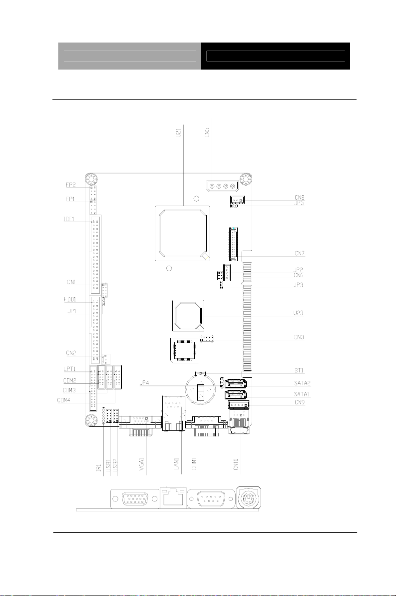
2.2 Location of Connectors and Jumpers
Component Side
Chapter 2 Quick Installation Guide 2-3
Page 17
Half-size SBC HSB-800P
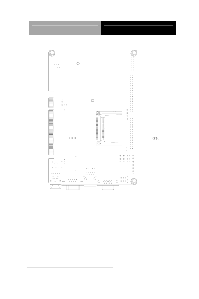
Solder Side
Chapter 2 Quick Installation Guide 2-4
Page 18

Half-size SBC HSB-800P
2.3 Mechanical Drawing
Component Side
Solder Side
Chapter 2 Quick Installation Guide 2-5
Page 19

Half-size SBC HSB-800P
2.4 List of Jumpers
The board has a number of jumpers that allow you to configure your
system to suit your application.
The table below shows the function of each of the board's jumpers:
Label Function
JP1 CFD Voltage 3.3V/5V Selection
JP2 LCD Clock and Power Selection
JP3
JP4
JP5 AT/ATX Power Type Selection
Inverter Voltage Selection
Clear CMOS
Chapter 2 Quick Installation Guide 2-6
Page 20

Half-size SBC HSB-800P
2.5 List of Connectors
The board has a number of connectors that allow you to configure
your system to suit your application. The table below shows the
function of each board's connectors:
Label
FP1 Front Panel Connector 1
FP2 Front Panel Connector 2
VGA1 VGA Display Connector
FDD1 Floppy Connector
IDE1 EIDE Connector
CFD1 Compact Flash Slot
COM1, COM3, COM4 RS-232 Serial Port Connector
COM2 RS-232/422/485 Serial Port Connector
IR1 IrDA Connector
LPT1 LPT Port Connector
USB1~2 USB Connector
LAN1
CN1
CN2 Fan Connector
CN3
CN5 AT Power_5V, 12V Connector
CN6
Function
10/100 or 100/1000 Base-TX Ethernet
Connector
Digital I/O
Audio Input/Output
LCD Inverter Power Connector
CN7
CN8 +5VSB Power Connector
CN9 Internal Keyboard Connector
CN10 PS/2 Keyboard/Mouse Connector
LVDS1 Connector
Chapter 2 Quick Installation Guide 2-7
Page 21

Half-size SBC HSB-800P
2.6 Setting Jumpers
You configure your card to match the needs of your application by
setting jumpers. A jumper is the simplest kind of electric switch. It
consists of two metal pins and a small metal clip (often protected by
a plastic cover) that slides over the pins to connect them. To “close”
a jumper you connect the pins with the clip.
To “open” a jumper you remove the clip. Sometimes a jumper will
have three pins, labeled 1, 2 and 3. In this case you would connect
either pins 1 and 2 or 2 and 3.
3
2
1
Open Closed Closed 2-3
A pair of needle-nose pliers may be helpful when working with
jumpers.
If you have any doubts about the best hardware configuration for
your application, contact your local distributor or sales
representative before you make any change.
Generally, you simply need a standard cable to make most
connections.
Chapter 2 Quick Installation Guide 2-8
Page 22

Half-size SBC HSB-800P
2.7 CFD Voltage 3.3V/5V Selection (JP1)
JP1 Function
1-2 3.3V
2-3 5V (default)
2.8 LCD Clock and Power Selection (JP2)
JP2 Function
1-3 Normal (default)
3-5 Inverse
2-4 +5Vlcd
4-6 +3Vlcd (default)
2.9 Inverter Voltage Selection (JP3)
JP3 Function
1-2 +12V (default)
2-3 +5V
2.10 Clear CMOS (JP4)
JP4 Function
1-2 Normal (default)
2-3 Clear CMOS
2.11 AT/ATX Power Type Selection (JP5)
JP5 Function
1-2 ATX Power Supply (default)
AT Power Supply
Note: Only AT function w/o backplane.
Chapter 2 Quick Installation Guide 2-9
Page 23

Half-size SBC HSB-800P
2.12 Front Panel Connector (FP1)
Pin Signal Pin Signal
1 Power On Button (+) 2
3 Power On Button (-) 4
5
IDE LED (+)
7
IDE LED (-)
Reset Switch (+)
Reset Switch (-)
6
Power LED (+)
8
Power LED (-)
2.13 Front Panel Connector (FP2)
Pin Signal Pin Signal
1
External Speaker (+)
3
N.C
5
Internal Buzzer (-) (Default)
7
External Speaker (-) (Default)
Note: Internal Buzzer Enable: Close Pin 5,7
2
Key Board Lock (+)
4
GND
6
I2C Bus SMB Clock
8
I2C Bus SMB Data
2.14 RS-232 Serial Port Connector (COM1, COM3, COM4)
Pin Signal Pin Signal
1 DCD 2 RXD
3 TXD 4 DTR
5 GND 6 DSR
7 RTS 8 CTS
9 RI 10 N.C
Chapter 2 Quick Installation Guide 2-10
Page 24

Half-size SBC HSB-800P
2.15 RS-232/422/485 Serial Port Connector (COM2)
Pin Signal Pin Signal
1 DCD (422TXD-/485DATA-) 2 RXD (422RXD+)
3 TXD (422TXD+/485DATA+) 4 DTR (422RXD-)
5 GND 6 DSR
7 RTS 8 CTS
9 RI/+12V 10 N.C
2.16 IrDA Connector (IR1)
Pin Signal
1 +5V
2 N.C
3 IRRX
4 GND
5 IRTX
6 N.C
2.17 Digital I/O (CN1)
Pin Signal Pin Signal
1 IN0 2 IN1
3 IN2 4 IN3
5 OUT0 6 OUT1
7 OUT2 8 OUT3
9 +5V 10 GND
BIOS
Setting
DIO-1 CN1 Pin1 Bit 7 U7 Pin20
Connector Definition Address IT8781 GPIO Setting
Chapter 2 Quick Installation Guide 2-11
Page 25

Half-size SBC HSB-800P
DIO-2 CN1 Pin2 Bit6 U7 Pin21
DIO-3 CN1 Pin3 Bit5 U7 Pin22
DIO-4 CN1 Pin4 Bit4 U7 Pin23
DIO-5 CN1 Pin5 Bit3 U7 Pin24
DIO-6 CN1 Pin6 Bit2 U7 Pin25
DIO-7 CN1 Pin7 Bit1 U7 Pin26
DIO-8 CN1 Pin7 Bit0 U7 Pin27
2.18 LPT Port Connector (LPT1)
Pin Signal Pin Signal
1 #STROBE 2 #AFD
3 DATA0 4 #ERROR
5 DATA1 6 #INIT
7 DATA2 8 #SLIN
9 DATA3 10 GND
11 DATA4 12 GND
13 DATA5 14 GND
15 DATA6 16 GND
17 DATA7 18 GND
19 #ACK 20 GND
21 BUSY 22 GND
23 PE 24 GND
25 SELECT 26 GND
2.19 USB Connector (USB1~2)
Pin Signal
1 +5V 2
3 USBD1- 4
5 USBD1+ 6 USBD1+
Chapter 2 Quick Installation Guide 2-12
GND
GND
Page 26

Half-size SBC HSB-800P
7 GND 8 USBD19 GND 10 +5V
2.20 Fan Connector (CN2)
Pin Signal
1 GND
2 +5V
3 Speed Sense
2.21 Audio Input/ Output (CN3)
Pin Signal Pin Signal
1 AC_RST# 2 AC_SYNC
3 AC_SDIN0 4
5 GND 6 AC_BITCLK
7 GND 8 +5V
9 N.C 10 +3.3V
AC_SDOUT
2.22 AT Power_5V, 12V Connector (CN5)
Pin Signal
1 +5V
2 GND
3 GND
4 +12V
2.23 LCD Inverter (CN6)
Pin Signal
1 12V / 5V
2 GND
Chapter 2 Quick Installation Guide 2-13
Page 27

Half-size SBC HSB-800P
3 VCON
4 GND
5 BKL_EN
2.24 LVDS1 (CN7)
Pin Signal Pin Signal
1 BKL_EN 2 N.C
3 VLCD 4 GND
5 LVDS_CLK# 6 LVDS_CLK
7 VLCD 8 GND
9 TX0# 10 TX0
11 TX1# 12 TX1
13 TX2# 14 TX2
15 TX3# 16 TX3
17 N.C 18 N.C
19 N.C 20 N.C
21 N.C 22 N.C
23 N.C 24 N.C
25 N.C 26 N.C
27 VLCD 28 GND
29 N.C 30 N.C
2.25 +5VSB Power Connector (CN8)
Pin Signal
1 PS_ON#
2 +5V
3 +5VSB
Chapter 2 Quick Installation Guide 2-14
Page 28

Half-size SBC HSB-800P
2.26 Internal Keyboard Connector (CN9)
Pin Signal
1 KB_CLK
2 KB_DATA
3 N.C
4 GND
5 +5V
2.27 PS2 Keyboard/Mouse Connector (CN10)
Pin Signal
1 KB_DATA
2 MS-DATA
3 GND
4 +5V
5 KB_CLK
6 MS_CLK
Chapter 2 Quick Installation Guide 2-15
Page 29

Half-size SBC HSB-800P
Below Table for China RoHS Requirements
产品中有毒有害物质或元素名称及含量
AAEON Main Board/ Daughter Board/ Backplane
有毒有害物质或元素
部件名称
印刷电路板
及其电子组件
外部信号
连接器及线材
O:表示该有毒有害物质在该部件所有均质材料中的含量均在
SJ/T 11363-2006 标准规定的限量要求以下。
X:表示该有毒有害物质至少在该部件的某一均质材料中的含量超出
SJ/T 11363-2006 标准规定的限量要求。
备注:此产品所标示之环保使用期限,系指在一般正常使用状况下。
铅
(Pb)汞 (Hg)镉 (Cd)
× ○ ○ ○ ○ ○
× ○ ○ ○ ○ ○
六价铬
(Cr(VI))
多溴联苯
(PBB)
多溴二苯醚
(PBDE)
Chapter 2 Quick Installation Guide 2-16
Page 30

Half-size SBC HSB-800P
Chapter
3
Award
BIOS Setup
Chapter 3 Award BIOS Setup 3-1
Page 31

Half-size SBC HSB-800P
3.1 System Test and Initialization
These routines test and initialize board hardware. If the routines
encounter an error during the tests, you will either hear a few short
beeps or see an error message on the screen. There are two kinds
of errors: fatal and non-fatal. The system can usually continue the
boot up sequence with non-fatal errors. Non-fatal error messages
usually appear on the screen along with the following instructions:
Press <F1> to RESUME
Write down the message and press the F1 key to continue the boot
up sequence.
System configuration verification
These routines check the current system configuration against the
values stored in the CMOS memory. If they do not match, the
program outputs an error message. You will then need to run the
BIOS setup program to set the configuration information in memory.
There are three situations in which you will need to change the
CMOS settings:
1. You are starting your system for the first time
2. You have changed the hardware attached to your system
3. The CMOS memory has lost power and the configuration
information has been erased.
The HSB-800P CMOS memory has an integral lithium battery
backup for data retention. However, you will need to replace the
complete unit when it finally runs down.
Chapter 3 Award BIOS Setup 3-2
Page 32

Half-size SBC HSB-800P
3.2 Award BIOS Setup
Awards BIOS ROM has a built-in Setup program that allows users
to modify the basic system configuration. This type of information is
stored in battery-backed CMOS RAM so that it retains the Setup
information when the power is turned off.
Entering setup
Power on the computer and press <Del> immediately. This will
allow you to enter Setup.
Standard CMOS Features
Use this menu for basic system configuration. (Date, t ime, IDE,
etc.)
Advanced BIOS Features
Use this menu to set the advanced features available on your
system.
Advanced Chipset Features
Use this menu to change the values in the chipset registers and
optimize your system performance.
Integrated Peripherals
Use this menu to specify your settings for integrated peripherals.
(Primary slave, secondary slave, keyboard, mouse etc.)
Power Management Setup
Use this menu to specify your settings for power management.
(HDD power down, power on by ring etc.)
PnP/PCI Configurations
This entry appears if your system supports PnP/PCI.
Chapter 3 Award BIOS Setup 3-3
Page 33

Half-size SBC HSB-800P
PC Health Status
This menu shows you the status of PC.
Load Fail-Safe Defaults
Use this menu to load the BIOS default values for the minimal/
stable performance for your system to operate.
Load Optimized Defaults
Use this menu to load the BIOS default values that are factory
settings for optimal performance system operations. While AWARD
has designated the custom BIOS to maximize performance, the
factory has the right to change these defaults to meet their needs.
Set Supervisor/User Password
Use this menu to set Supervisor/User Passwords.
Save and Exit Setup
Save CMOS value changes to CMOS and exit setup.
Exit Without Saving
Abandon all CMOS value changes and exit setup.
For more detailed information, you can refer to the "AAEON
BIOS Item Description.pdf" file in the CD for the meaning of
each setting in this chapter.
Chapter 3 Award BIOS Setup 3-4
Page 34

Half-size SBC HSB-800P
Chapter
4
Driver
Installation
Chapter 4 Driver Installation 4-1
Page 35

Half-size SBC HSB-800P
The HSB-800P comes with a CD-ROM that contains all drivers your
need.
Follow the sequence below to install the drivers:
Step 1 – Install VGA Driver
Step 2 – Install AES Driver
Step 3 – Install LAN Driver
Step 4 – Install Audio Driver
Step 5 – Install SATA Driver
Please read following instructions for detailed installations.
Chapter 4 Driver Installation 4-2
Page 36

Half-size SBC HSB-800P
4.1 Installation:
Insert the HSB-800P CD-ROM into the CD-ROM Drive. And install
the drivers from Step 1 to Step 5 in order.
Step 1 –Install VGA Driver
Place the Driver CD-ROM into your CD-ROM drive and follow
the steps below to install.
1. Click on Start button
2. Click on Settings button
3. Click on Control Panel button
4. Click on System button
5. Select Hardware and click on Device Manager…
6. Double click on Video Controller (VGA Compatible)
7. Click on Update Driver…
8. Click on Next
9. Select Search for a suitable driver…, then click on Next
10. Select Specify a location, then click on Next
11. Click on Browse
12. Select “lx_win” file from CD-ROM (Driver/Step 1 –
Display) then click on Open
13. Click on OK
14. Click on Next
15. Click on Yes
16. Click on Finish
Chapter 4 Driver Installation 4-3
Page 37

Half-size SBC HSB-800P
Step 2 –Install AES Driver
Place the Driver CD-ROM into your CD-ROM drive and follow
the steps below to install.
1. Click on Start button
2. Click on Settings button
3. Click on Control Panel button
4. Click on System button
5. Select Hardware and click on Device Manager…
6. Double click on Entertainment Encryption/Decryption
Controller
7. Click on Update Driver…
8. Click on Next
9. Select Search for a suitable driver…, then click on Next
10. Select Specify a location, then click on Next
11. Click on Browse
12. Select “lxaes” file from CD-ROM (Drivers/Step 2 –
AES) then click on Open
13. Click on OK
14. Click on Next
15. Click on Yes
16. Click on Finish
Step 3 – Install LAN Driver
1. Click on the Step 3 –LAN folder and select the folder of
Windows
Chapter 4 Driver Installation 4-4
Page 38

Half-size SBC HSB-800P
2. Double click on Setup.exe
3. Follow the instructions that the window shows
4. The system will help you install the driver automatically
Step 4– Install Audio Driver
Place the Driver CD-ROM into your CD-ROM drive and follow
the steps below to install.
1. Click on Start button
2. Click on Settings button
3. Click on Control Panel button
4. Click on System button
5. Select Hardware and click on Device Manager…
6. Double click on Multimedia Audio Controller
7. Click on Update Driver…
8. Click on Next
9. Select Search for a suitable driver…, then click on Next
10. Select Specify a location, then click on Next
11. Click on Browse
12. Select “LXWDMAu” file from CD-ROM (Driver/Step 4–
Audio) then click on Open
13. Click on OK
14. Click on Next
15. Click on Yes
16. Click on Finish
Chapter 4 Driver Installation 4-5
Page 39

Half-size SBC HSB-800P
Step 5 – Install SATA Driver
Place the Driver CD-ROM into your CD-ROM drive and pull up
the CD-ROM file on your screen.
1. Click on Start button
2. Click on Settings button
3. Click on Control Panel button
4. Click on System button
5. Select Hardware and click on Device Manager…
6. Double click on SCSI and RAID Controller
7. Click on Update Driver…
8. Click on Next
9. Select Search for a suitable driver…, then click on Next
10. Select Specify a location, then click on Next
11. Click on Browse
12. Select “silicon Image Sil3112 SATALink Controller” file
from CD-ROM (Driver/Step 5- SATA Driver) then click on
Open
13. Click on OK
14. Click on Next
15. Click on Yes
16. Click on Finish
Chapter 4 Driver Installation 4-6
Page 40

Half-size SBC HSB-800P
A
Appendix
Programming the
Watchdog Timer
Appendix A Programming the Watchdog Timer A - 1
Page 41

Half-size SBC HSB-800P
A.1 Programming
HSB-800P utilizes ITE 8712 chipset as its watchdog timer controller.
( K version )
Below are the procedures to complete its configuration and the
AAEON intial watchdog timer program is also attached based on
which you can develop customized program to fit your application.
Configuring Sequence Description
After the hardware reset or power-on reset, the ITE 8712 enters the
normal mode with all logical devices disabled except KBC.
There are three steps to complete the configuration setup: (1) Enter
the MB PnP Mode; (2) Modify the data of configuration registers; (3)
Appendix A Programming the Watchdog Timer A - 2
Page 42

Half-size SBC HSB-800P
Exit the MB PnP Mode. Undesired result may occur if the MB PnP
Mode is not exited normally.
(1) Enter the MB PnP Mode
To enter the MB PnP Mode, four special I/O write operations are to
be performed during Wait for Key state. To ensure the initial state of
the key-check logic, it is necessary to perform four write opera -tions
to the Special Address port (2EH). Two different enter keys are
provided to select configuration ports (2Eh/2Fh) of the next step.
Address Port Data Port
87h, 01h, 55h, 55h: 2Eh 2Fh
(2) Modify the Data of the Registers
All configuration registers can be accessed after entering the MB
PnP Mode. Before accessing a selected register, the content of
Index 07h must be changed to the LDN to which the register
belongs, except some Global registers.
(3) Exit the MB PnP Mode
Set bit 1 of the configure control register (Index=02h) to 1 to exit the
MB PnP Mode.
WatchDog Timer Configuration Registers
LDN Index R/W Reset Configuration Register or Action
All 02H W N/A Configuration Control
07H 71H R/W 00H WatchDog Timer Contro l Register
07H 72H R/W 00H WatchDog Timer Configuration Register
07H 73H R/W 00H WatchDog Timer Time-out Value (LSB)
Register
07H 74H R/W 00H WatchDog Timer Time-out Value (MSB)
Register
Configure Control (Index=02h)
This register is write only. Its values are not sticky; that is to say, a
hardware reset will automatically clear the bits, and does not
Appendix A Programming the Watchdog Timer A - 3
Page 43

Half-size SBC HSB-800P
require the software to clear them.
Bit Description
7-2 Reserved
1 Returns to the Wait for Key state. This bit is used when the
configuration sequence is completed.
0 Resets all logical devices and restores configuration registers
to their power-on states.
WatchDog Timer Control Register (Index=71h, Default=00h)
Bit Description
7 WDT is reset upon a CIR interrupt
6 WDT is reset upon a KBC (Mouse) interrupt
5 WDT is reset upon a KBC (Keyboard) interrupt
4 WDT is reset upon a read or a write to the Game port base
address
3-2 Reserved
1 Force Time-out. This bit is self-clearing
0 WDT status
1: WDT value reaches 0
0: WDT value is not 0
WatchDog Timer Configuration Register (Index=72h,
Default=00h)
Bit Description
7 WDT Time-out value select
1: Second
0: Minute
6 WDT output through KRST (pulse) enable
5 WDT Time-out value Extra select
1: 4s.
0: Determine by WDT Time-out value select (bit7 of this
register)
4 WDT output through PWROK1/PWROK2 (pulse) enable
3 Select the interrupt level
note
for WDT
Appendix A Programming the Watchdog Timer A - 4
Page 44

Half-size SBC HSB-800P
WatchDog Timer Time-out Value (LSB) Register (Index=73h,
Default=00h)
Bit Description
7-0 WDT Time-out value 7-0
WatchDog Timer Time-out Value (MSB) Register (Index=74h,
Default=00h)
Bit Description
7-0 WDT Time-out value 15-8
Appendix A Programming the Watchdog Timer A - 5
Page 45

Half-size SBC HSB-800P
A.2 ITE8712 Watchdog Timer Initial Program
.MODEL SMALL
.CODE
Main:
CALL Enter_Configuration_mode
CALL Check_Chip
mov cl, 7
call Set_Logic_Device
;time setting
mov cl, 10 ; 10 Sec
dec al
Watch_Dog_Setting:
;Timer setting
mov al, cl
mov cl, 73h
call Superio_Set_Reg
;Clear by keyboard or mouse interrupt
mov al, 0f0h
mov cl, 71h
call Superio_Set_Reg
;unit is second.
mov al, 0C0H
mov cl, 72h
call Superio_Set_Reg
Appendix A Programming the Watchdog Timer A - 6
Page 46

Half-size SBC HSB-800P
; game port enable
mov cl, 9
call Set_Logic_Device
Initial_OK:
CALL Exit_Configuration_mode
MOV AH,4Ch
INT 21h
Enter_Configuration_Mode PROC NEAR
MOV SI,WORD PTR CS:[Offset Cfg_Port]
MOV DX,02Eh
MOV CX,04h
Init_1:
MOV AL,BYTE PTR CS:[SI]
OUT DX,AL
INC SI
LOOP Init_1
RET
Enter_Configuration_Mode ENDP
Exit_Configuration_Mode PROC NEAR
MOV AX,0202h
CALL Write_Configuration_Data
Appendix A Programming the Watchdog Timer A - 7
Page 47

Half-size SBC HSB-800P
RET
Exit_Configuration_Mode ENDP
Check_Chip PROC NEAR
MOV AL,20h
CALL Read_Configuration_Data
CMP AL,87h
JNE Not_Initial
MOV AL,21h
CALL Read_Configuration_Data
CMP AL,12h
JNE Not_Initial
Need_Initial:
STC
RET
Not_Initial:
CLC
RET
Check_Chip ENDP
Read_Configuration_Data PROC NEAR
MOV DX,WORD PTR CS:[Cfg_Port+04h]
OUT DX,AL
Appendix A Programming the Watchdog Timer A - 8
Page 48

Half-size SBC HSB-800P
MOV DX,WORD PTR CS:[Cfg_Port+06h]
IN AL,DX
RET
Read_Configuration_Data ENDP
Write_Configuration_Data PROC NEAR
MOV DX,WORD PTR CS:[Cfg_Port+04h]
OUT DX,AL
XCHG AL,AH
MOV DX,WORD PTR CS:[Cfg_Port+06h]
OUT DX,AL
RET
Write_Configuration_Data ENDP
Superio_Set_Reg proc near
push ax
MOV DX,WORD PTR CS:[Cfg_Port+04h]
mov al,cl
out dx,al
pop ax
inc dx
out dx,al
ret
Superio_Set_Reg endp.Set_Logic_Device proc near
Appendix A Programming the Watchdog Timer A - 9
Page 49

Half-size SBC HSB-800P
Set_Logic_Device proc near
push ax
push cx
xchg al,cl
mov cl,07h
call Superio_Set_Reg
pop cx
pop ax
ret
Set_Logic_Device endp
;Select 02Eh->Index Port, 02Fh->Data Port
Cfg_Port DB 087h,001h,055h,055h
DW 02Eh,02Fh
END Main
Note: Interrupt level mapping
0Fh-Dh: not valid
0Ch: IRQ12
.
.
03h: IRQ3
02h: not valid
01h: IRQ1
00h: no interrupt selected
Appendix A Programming the Watchdog Timer A - 10
Page 50

Half-size SBC HSB-800P
Appendix
B
I/O Information
Appendix B I/O Information B-1
Page 51

Half-size SBC HSB-800P
B.1 I/O Address Map
Appendix B I/O Information B-2
Page 52

Half-size SBC HSB-800P
B.2 Memory Address Map
B.3 IRQ Mapping Chart
B.4 DMA Channel Assignments
Appendix B I/O Information B-3
Page 53

Half-Size Board HSB-800P
Appendix
C
Mating Connector
Appendix C Mating Connector C - 1
Page 54

Half-Size Board HSB-800P
A
C.1 List of Mating Connectors and Cables
The table notes mating connectors and available cables.
Connector
Label
Function
Mating Connector
Vendor Model no
vailable
Cable
Cable P/N
IDE1 IDE
Connector
SATA1 SATA
Connector
SATA2 SATA
Connector
FDD1 Floppy
Connector
LPT1 Parallel
Port
Connector
FP1 Front
Panel
Connector
FP2 Front
Panel
Connector
USB1 USB Pin
Header
USB2 USB Pin
Header
CN1 Digital I/O
Pin Header
CN3 Audio Pin
Header
CN2 FAN
Connector
Catch
Electronics
TECHBEST 161S01-025A SATA
TECHBEST 161S01-025A SATA
Catch
Electronics
Catch
Electronics
JIH VEI
Electronics
JIH VEI
Electronics
JIH VEI
Electronics
JIH VEI
Electronics
JIH VEI
Electronics
JIH VEI
Electronics
Catch
Electronics
1137-020-40
SA
1137-000-34
SA
1147-000-26S LPT
21B22564-X
XS10B-01G
-6/3-VXX
21B22564-X
XS10B-01G
-6/3-VXX
21B22050-X
XS10B-01G
-4/2.8
21B22050-X
XS10B-01G
-4/2.8
21B22050-X
XS10B-01G
-4/2.8
21N22050-1
0S10B-01G4/2.8-V1-G
1190-700-03S N/A
IDE Cable 1701400453
1709070800
Cable
1709070800
Cable
Floppy
Disk Drive
Cable
Cable
N/A
N/A
USB
Cable
USB
Cable
N/A
N/A
1701340704
1701260307
1709100201
1709100201
Appendix C Mating Connector C - 2
Page 55

Half-Size Board HSB-800P
LAN1 Ethernet
Connector
IR1 IrDA
Connector
CN10 Mini-Din
PS/2
Connector
CN9 KB Pin
Header
COM1 COM Port
Connector
COM2 Serial Port
Box
Header
COM3 Serial Port
Box
Header
COM4 Serial Port
Box
Header
VGA1 CRT
Display
Connector
CN7 LVDS
Connector
CN6 Inverter
Connector
CN8 ATX Power
Connector
with BP
CN5 Big 4P
Power
Connector
UDE RT1-165AB
N/A
B1A
JIH VEI
Electronics
21B12050-X
XS10B-01G
N/A
-4/2.8
CONTEK MAN3061F1
G401
KB/MS
Cable
1700060192
HO-BASE 2503-WS-5 N/A
Astron DB6A-09-A
N/A
MGN1-R
Catch
Electronics
1147-000-10S Serial
Port
1701100305
Cable
Catch
Electronics
1147-000-10S Serial
Port
1701100305
Cable
Catch
Electronics
1147-000-10S Serial
Port
1701100305
Cable
Catch
Electronics
E-call 0110-01-553
3125-000-1
5SB
N/A
N/A
-300
Catch
1192-700-05S N/A
Electronics
Catch
1191-700-03S 1703030501
Electronics
HO-BASE 5082A-WS-4 N/A
Appendix C Mating Connector C - 3
 Loading...