

Page 1
SubCompact Board GENE-U15B
Intel® Atom™Z5x0P Processor
®
System Controller Hub US15WP
Intel
10/100/1000Base-TX
1 SATA 3.0Gb/s, Onboard SST SSD
4 COM, 6 USB2.0, Digital I/O
1 Mini Card
GENE-U15B
GENE-U15B Manual Rev.A 2
June 2011
nd
Ed.
Page 2

SubCompact Board GENE-U15B
Copyright Notice
This document is copyrighted, 2011. All rights are reserved. The
original manufacturer reserves the right to make improvements to the
products described in this manual at any time without notice.
No part of this manual may be reproduced, copied, translated, or
transmitted in any form or by any means without the prior written
permission of the original manufacturer. Information provided in this
manual is intended to be accurate and reliable. However, the original
manufacturer assumes no responsibility for its use, or for any infringements upon the rights of third parties that may result from its
use.
The material in this document is for product information only and is
subject to change without notice. While reasonable efforts have been
made in the preparation of this document to assure its accuracy,
AAEON assumes no liabilities resulting from errors or omissions in
this document, or from the use of the information contained herein.
AAEON reserves the right to make changes in the product design
without notice to its users.
i
Page 3

SubCompact Board GENE-U15B
Acknowledgments
All other products’ name or trademarks are properties of their
respective owners.
Award is a trademark of Award Software International, Inc.
CompactFlash™ is a trademark of the Compact Flash
Association.
Intel
Microsoft Windows
ITE is a trademark of Integrated Technology Express, Inc.
IBM, PC/AT, PS/2, and VGA are trademarks of International
SoundBlaster is a trademark of Creative Labs, Inc.
All other product names or trademarks are properties of their
respective owners.
®
, Atom are trademarks of Intel® Corporation.
®
is a registered trademark of Microsoft Corp.
Business Machines Corporation.
ii
Page 4

SubCompact Board GENE-U15B
Packing List
Before you begin installing your card, please make sure that the
following materials have been shipped:
1700060157 Keyboard & Mouse Cable
CD-ROM for manual (in PDF format) and drivers
GENE-U15B
If any of these items should be missing or damaged, please
contact your distributor or sales representative immediately.
iii
Page 5

SubCompact Board GENE-U15B
Contents
Chapter 1 General Information
1.1 Introduction................................................................ 1-2
1.2 Features....................................................................1-3
1.3 Specifications............................................................1-4
Chapter 2 Quick Installation Guide
2.1 Safety Precautions....................................................2-2
2.2 Location of Connectors & Jumpers...........................2-3
2.3 Mechanical Drawing..................................................2-5
2.4 List of Jumpers..........................................................2-7
2.5 List of Connectors .....................................................2-7
2.6 Setting Jumpers ........................................................2-9
2.7 LVDS Inverter Voltage Selection (JP1).....................2-10
2.8 LVDS Panel +5V/+3.3V Selection (JP2)...................2-10
2.9 LVDS-Inverter +5V/+12V Selection (JP3).................2-10
2.10 COM2 Ring/+5V/+12V Selection (JP4)...................2-10
2.11 Touch Panel 4/5/8-wire Selection (JP5).................. 2-10
2.12 CPLD Reset Selection (JP6)...................................2-11
2.13 Auto Power Button / Front Panel Button Selection (JP7)
.........................................................................................2-11
2.14 CMOS Selection (JP8)............................................2-11
2.15 CRT Always On Disable/ Enable (JP9)................... 2-11
2.16 LVDS LCD Connector (CN5) .................................. 2-11
iv
Page 6

SubCompact Board GENE-U15B
2.17 LVDS Inverter +5V/+12V Connector (CN6) ............2-12
2.18 Touch Panel Connector (CN8)................................ 2-12
2.19 RS-232 Serial Port Connector (CN11)....................2-13
2.20 RS-232/422/485 Serial Port Connector (CN12)......2-13
2.21 Fan Connector (CN17)............................................ 2-14
2.22 RS-232 Serial Port Connector (CN18).................... 2-14
2.23 PS2 Keyboard/Mouse Connector (CN19)............... 2-14
2.24 RS-232 Serial Port Connector (CN20).................... 2-14
2.25 CPLD Programming Connector (CN21).................. 2-15
2.26 12V Power Jack Connector (CN27)........................ 2-15
2.27 Output +5V_DUAL / PSON# /SM Bus Connector (CN28)
.........................................................................................2-15
2.28 Front Panel Connector (CN29) ...............................2-16
2.29 USB Connector (CN30)........................................... 2-16
2.30 Digital I/O Connector (CN31).................................. 2-16
2.31 5V Power Jack Connector (CN32).......................... 2-17
2.32 USB Connector (CN34)........................................... 2-17
2.33 Output Power Connector (CN36)............................ 2-18
2.34 Audio 2.1 Channel Connector (CN37)....................2-18
2.35 LPC Connector (CN39)...........................................2-18
2.36 VGA Display Connector (CN40).............................. 2-19
2.37 +5VSB External Input Connector (CN41) ............... 2-19
Chapter 3 Award BIOS Setup
3.1 System Test and Initialization. ..................................3-2
3.2 Award BIOS Setup.................................................... 3-3
v
Page 7

SubCompact Board GENE-U15B
Chapter 4 Driver Installation
4.1 Installation................................................................. 4-3
Appendix A Programming The Watchdog Timer
A.1 Programming .........................................................A-2
Appendix B I/O Information
B.1 I/O Address Map....................................................B-2
B.2 Memory Address Map............................................B-3
B.3 IRQ Mapping Chart................................................B-4
B.4 DMA Channel Assignments...................................B-4
Appendix C Mating Connector
C.1 List of Mating Connectors and Cables.................. C-2
Appendix D DIO
D.1 DIO........................................................................ D-2
vi
Page 8

SubCompact Board GENE-U15B
Information
Chapter
1
General
Chapter 1 General Information 1- 1
Page 9

SubCompact Board GENE-U15B
1.1 Introduction
AAEON, a leading embedded boards manufacturer, is pleased to
announce the debut of their new generation 3.5” SubCompact
Board—GENE-U15B. The GENE-U15B is a cutting-edge product that
provides high performance and low power consumption in the
embedded market.
GENE-U15B adopts the latest Intel
®
Atom Z530P/Z510P processor
and the system memory deploys with SODIMM DDR2 400/533 up to
2GB. In addition, Intel
®
82574L supports one 10/100/100Base-TX
that allows faster network connections. This model applies one Mini
Card and onboard 4/5/8-wire resistive touch screen controller.
Moreover, one SATA 3.0Gb/s and onboard SSD up 4GB are
configured on the GENE-U15B. GENE-U15B also equips six USB2.0,
four COM, one keyboard and one mouse ports for flexible I/O
expansions.
The display of GENE-U15B supports CRT/LCD simultaneous/ dual
view displays and up to 24-bit single channel LVDS. This brand new
SubCompact board is developed to cater to the requirements of
Automation, Medical, ticket machine, transportation, gaming, KIOSK,
and POS/POI applications.
Chapter 1 General Information 1- 2
Page 10

SubCompact Board GENE-U15B
1.2 Features
z Intel® Atom™ Z530P/Z510P Processor
z Intel
®
System Controller Hub US15WP
z DDR2 400/533 SODIMM, Max. 2 GB
z Gigabit Ethernet x 1
z CRT, 24-Bit Single Channel LVDS LCD
z 2CH HD Audio
z SATA 3.0Gb/s x 1, Onboard SSD Up To 4GB
z USB2.0 x 6, COM x 4, 8-Bit Digital I/O
z Onboard 4/5/8-wire Resistive Touch Screen Controller
z Mini Card x 1
z +12V or +5V (Optional) Only Operation
Chapter 1 General Information
1 - 3
Page 11

SubCompact Board GENE-U15B
1.3 Specifications
System
z Form Factor 3.5”
z Processor Intel
z System Memory 200-pin DDR2 SODIMM x 1, Max.
z Chipset Intel
z I/O Chipset SMSC SCH3114-NU
z Ethernet Intel
z BIOS Award Plug & Play PLCC Type – 1 MB
z Wake On LAN Yes
®
Atom™Z530P 1.6 GHz, Z510P
1.1 GHz
2GB (DDR2 400/533)
®
System Controller Hub US15WP
®
82574L, 10/100/1000Base-TX,
RJ-45 x 1
ROM
z Watchdog Timer Generates a time-out system reset
z H/W Monitor
Chipset
z Expansion Interface Mini Card x 1, LPC Bus
z Battery Lithium battery
z Power Requirement +12V or +5V (optional), AT/ATX
z Board Size 5.75”(L) x 4”(W) (146mm x 101.6mm)
z Gross Weight 0.88 lb (0.4 kg)
z Operating 32˚F~ 140˚F (0˚C ~ 60˚C)
Chapter 1 General Information 1- 4
Supports power supply voltages and
temperature monitoring
Page 12

SubCompact Board GENE-U15B
Temperature
z Storage
-40˚F~ 176˚F (-40˚C ~ 80˚C)
Temperature
z Operating Humidity 0%~90% relative humidity,
non-condensing
z MTBF (Hours) 700,000
Display: Supports CRT/LCD simultaneous/dual view displays
z Chipset Intel
®
Z5x0P integrated
z Memory Shared system memory up to 256
MB
z Resolution Up to 1280x1024 for VGA;
Up to 1366x768 for LCD
z LCD Interface Up to 24-bit single channel LVDS
I/O
z Storage SATA 3.0Gb/s x 1,
Onboard SST SSD up to 4GB
z Serial Port RS-232 x 3, RS-232/422/485
(auto flow) x 1
z USB Port USB2.0 x 6
z PS/2 Port Keyboard x 1, Mouse x 1
z Digital I/O Supports 8-bit (Programmable)
z Audio Line-in, Line-out, Mic-in
Chapter 1 General Information
1 - 5
Page 13

SubCompact Board GENE-U15B
Chapter
2
Quick
Inst
Chapter 2 Quick Installation Guide 2-1
allation
Guide
Page 14
SubCompact Board GENE-U15B
2.1 Safety Precautions
Always completely disconnect the power cord
from your board whenever you are working on
it. Do not make connections while the power is
on, because a sudden rush of power can
damage sensitive electronic components.
Always ground yourself to remove any static
charge before touching the board. Modern
electronic devices are very sensitive to static
electric charges. Use a grounding wrist strap at
all times. Place all electronic components on a
static-dissipative surface or in a static-shielded
bag when they are not in the chassis
Chapter 2 Quick Installation Guide 2-2
Page 15
SubCompact Board GENE-U15B
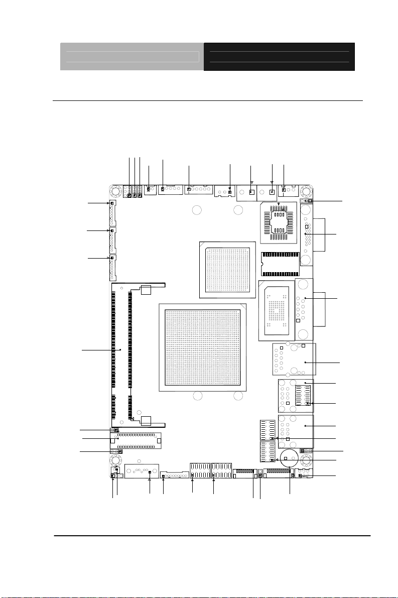
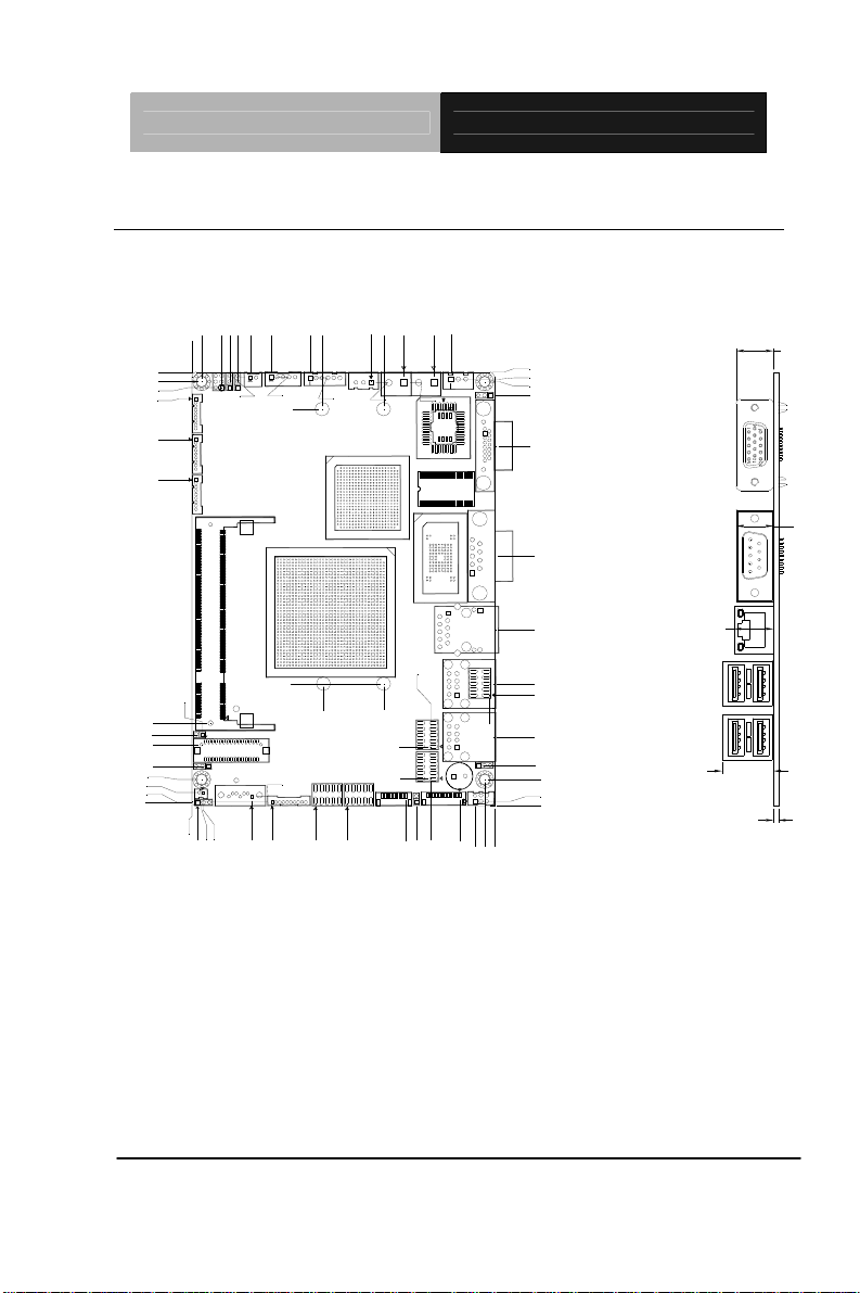
2.2 Location of Connectors and Jumpers
Component Side
JP2
JP4
JP3
CN36
CN6
CN28
CN41
CN32
CN27
CN17
CN12
CN18
CN20
CN2
JP6
CN5
JP1
JP9
CN40
CN11
CN7
CN30
CN34
CN22
CN35
JP7
CN31
CN19
JP8
BAT1
Chapter 2 Quick Installation Guide 2-3
CN37
CN23
CN21
CN29
JP5
CN8
CN39
Page 16
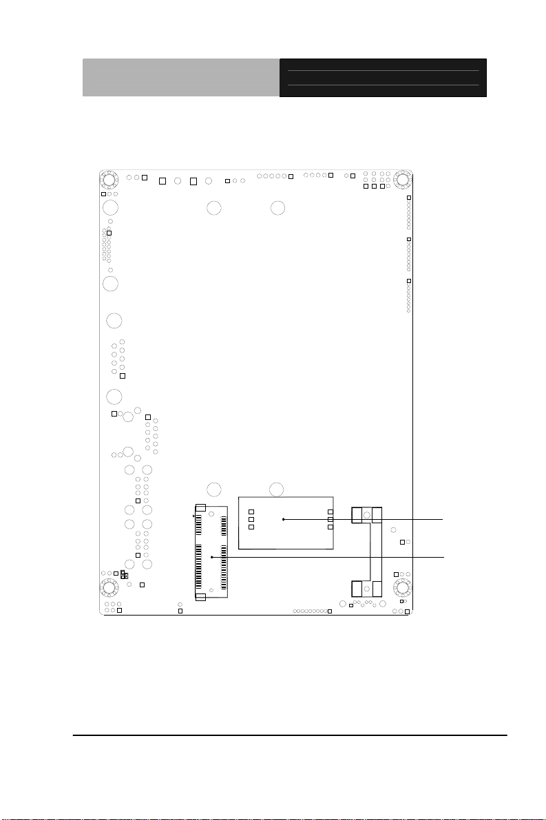
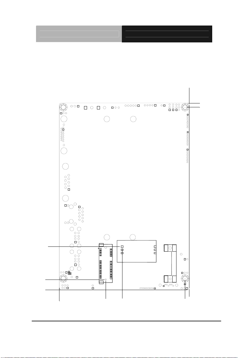
SubCompact Board GENE-U15B
Solder Side
Chapter 2 Quick Installation Guide 2-4
CN38
CN13
Page 17
SubCompact Board GENE-U15B
2.3 Mechanical Drawing
Component Side
146.05
142.82
140.78
137.01
123.40
109.78
27.89
24.01
20.70
13.34
8.89
4.51
1.25
1.21
98.12
101.60
98.37
101.60
144.19
99.74
86.32
74.97
91.64
88.98
82.06
144.34
133.56
41.13
3.17
74.62
81.57
98.37
97.94
61.93
60.17
57.88
144.05
57.44
49.50
41.41
19.94
9.19
37.18
142.53
37.18
14.60
30.42
20.39
146.05
143.62
142.75
142.45
21.26
26.19
29.81
21.26
11.55
138.16
120.96
84.24
59.26
41.03
37.26
23.22
1.76
13.70
8.89
1.54
0.00
0.00
6.44
3.17
(13.35)
(12.55)
(12.55)
(17.30)
(1.60)
Chapter 2 Quick Installation Guide 2-5
Page 18
SubCompact Board GENE-U15B
Solder Side
101.60
146.05
142.82
33.93
8.13
0.00
0.00
Chapter 2 Quick Installation Guide 2-6
36.30
49.15
98.37
101.60
Page 19

SubCompact Board GENE-U15B
2.4 List of Jumpers
The board has a number of jumpers that allow you to configure your
system to suit your application.
The table below shows the function of each of the board's jumpers:
Label Function
JP1 LVDS-Inverter Voltage Control Selection
JP2 LVDS-LCD +5V/+3.3V Selection
JP3 LVDS-Inverter +5V/+12V Selection
JP4 COM2 +5V/+12V/Ring Selection
JP5 Touch Panel 4/5/8-Wire Selection
JP6 CPLD Reset Selection
JP7 Auto Power Button / Front Panel Button Selection
JP8 Clear CMOS
JP9 CRT Always On Disable/Enable
2.5 List of Connectors
The board has a number of connectors that allow you to configure
your system to suit your application. The table below shows the
function of each board's connectors:
Label Function CN2 DDR2 SODIMM Connector
CN5 LVDS Panel Connector
CN6 LVDS-Inverter +5V/+12V Connector
CN7 LAN Connector
CN8 Touch Panel Connector
CN11 (COM1) RS-232 Serial Port Connector
CN12 (COM2) RS-232/422/485 Serial Port Connector
CN13 Mini Card Slot
Chapter 2 Quick Installation Guide 2-7
Page 20

SubCompact Board GENE-U15B
CN17 Fan Connector
CN18(COM3) RS-232 Serial Port Connector
CN19 Keyboard/Mouse Connector
CN20(COM4) RS-232 Serial Port Connector
CN21 CPLD Programming Connector
CN22 USB Connector
CN23 Serial-ATA Connector
CN27 12V input Power Jack Connector
CN28 Output +5V_DUAL / PSON# /SM Bus Connector
CN29 Front Panel Connector
CN30 USB Connector
CN31 Digital I/O Connector
CN32 5V input Power Jack Connector
CN34 USB Connector
CN35 USB Connector
CN36 Output Power Connector
CN37 Audio 2.1 Channel Connector
CN38 Sim Card Reader Connector
CN39 LPC Connector
CN40 VGA Connector
CN41
(Optional)
+5VSB External Input Connector
BAT1 Battery Connector
Note: USB 0-5 support USB1.1 and USB2.0, but USB 6-7 only support
USB2.0 only. CN35 is USB6-7 and supports USB2.0 only.
Chapter 2 Quick Installation Guide 2-8
Page 21

SubCompact Board GENE-U15B
2.6 Setting Jumpers
You configure your card to match the needs of your application by
setting jumpers. A jumper is the simplest kind of electric switch. It
consists of two metal pins and a small metal clip (often protected by a
plastic cover) that slides over the pins to connect them. To “close” a
jumper you connect the pins with the clip.
To “open” a jumper you remove the clip. Sometimes a jumper will
have three pins, labeled 1, 2 and 3. In this case you would connect
either pins 1 and 2 or 2 and 3.
3
2
1
Open Closed Closed 2-3
A pair of needle-nose pliers may be helpful when working with
jumpers.
If you have any doubts about the best hardware configuration for your
application, contact your local distributor or sales representative
before you make any change.
Generally, you simply need a standard cable to make most
connections.
Chapter 2 Quick Installation Guide 2-9
Page 22

SubCompact Board GENE-U15B
2.7 LVDS Inverter Voltage Control Selection (JP1)
JP1 Function
1-2 Voltage Control (Default)
2-3 NC
2.8 LVDS Panel +5V/+3.3V Selection (JP2)
JP2 Function
1-2 +5V
2-3 +3.3V (Default)
2.9 LVDS-Inverter +5V/+12V Selection (JP3)
JP3 Function
1-2 +12V
2-3 +5V (Default)
2.10 COM2 Ring/+5V/+12V Selection (JP4)
JP4 Function
1-2 +12V
3-4 +5V
5-6 Ring (Default)
2.11 Touch Panel 4/5/8-Wire Selection (JP5)
JP5 Function
1-2 4/8-wire (Default)
Open 5-wire
Chapter 2 Quick Installation Guide 2-10
Page 23

SubCompact Board GENE-U15B
2.12 CPLD Reset Selection (JP6)
JP6 Function
1-2 CPLD Reset
Open Normal (Default)
2.13 Auto Power Button / Front Panel Button Selection (JP7)
JP7 Function
1-2 Auto power button (Default)
2-3 Front panel button
2.14 CMOS Selection (JP8)
JP8 Function
1-2 Protected (Default)
2-3 Clear
2.15 CRT Always On Disable/ Enable (JP9)
JP9 Function
1-2 Disable (Default)
2-3 Enable
2.16 LVDS LCD Connector (CN5)
Pin Signal Pin Signal
1 L_BKLT_EN 2 BKL_CON
3 VLCD 4 GND
5 LA_CLK# 6 LA_CLK
7 VLCD 8 GND
9 LA_DATA#_0 10 LA_DATA_0
Chapter 2 Quick Installation Guide 2-11
Page 24

SubCompact Board GENE-U15B
11 LA_DATA#_1 12 LA_DATA_1
13 LA_DATA#_2 14 LA_DATA_2
15 LA_DATA#_3 16 LA_DATA_3
17 L_DDC_DATA 18 L_DDC_CLK
19 LB_DATA#_0 20 LB_DATA_0
21 LB_DATA#_1 22 LB_DATA_1
23 LB_DATA#_2 24 LB_DATA_2
25 LB_DATA#_3 26 LB_DATA_3
27 VLCD 28 GND
29 LB_CLK# 30 LB_CLK
2.17 LVDS Inverter +5V/+12V Connector (CN6)
Pin Signal
1 VCC-Inverter
2 BKL_CON
3 GND
4 GND
5 INV_EN
2.18 Touch Panel Connector (CN8)
Pin Signal
1 GND
2 Y-
3 Y+
4 X-
5 X+
6 SENSE
7 Y+
Chapter 2 Quick Installation Guide 2-12
Page 25

SubCompact Board GENE-U15B
8 X-
9 X+
2.19 RS-232 Serial Port Connector (CN11)
Pin Signal
1 DCDA
2 RXA
3 TXA
4 DTRA
5 GNDA
6 DSRA
7 RTSA
8 CTSA
9 RIA
2.20 RS-232/422/485 Serial Port Connector (CN12)
Pin Signal
1 DCDB
2 DSRB
3 RXB
4 RTSB
5 TXB
6 CTSB
7 DTRB
8 RIB
9 GND
Chapter 2 Quick Installation Guide 2-13
Page 26

SubCompact Board GENE-U15B
2.21 Fan Connector (CN17)
Pin Signal
1 GND
2 +12V
3 Speed Sense
2.22 RS-232 Serial Port Connector (CN18)
Pin Signal
1 DCDC
2 DSRC
3 RXC
4 RTSC
5 TXC
6 CTSC
7 DTRC
8 RIC
9 GND
2.23 PS2 Keyboard/Mouse Connector (CN19)
Pin Signal Pin Signal
1 KBDAT 2 KBCLK
3 KB_GND 4 +5V_DUAL
5 MSDAT 6 MSCLK
2.24 RS-232 Serial Port Connector (CN20)
Pin Signal
1 DCDD
Chapter 2 Quick Installation Guide 2-14
Page 27

SubCompact Board GENE-U15B
2 DSRD
3 RXD
4 RTSD
5 TXD
6 CTSD
7 DTRD
8 RID
9 GND
2.25 CPLD Programming Connector (CN21)
Pin Signal Pin Signal
1 TCK 2 GND
3 TDO 4 +3.3V_CPLD
5 TMS 6 NC
7 NC 8 NC
9 TDI 10 GND
2.26 12V Power Jack Connector (CN27)
Pin Signal
1 +12V_DUAL
2 GND
2.27 Output +5V_DUAL / PSON# /SM Bus Connector (CN28)
Pin Signal
1 SMBDAT_SBY
2 GND
3 SMBCLK_SBY
4 GND
Chapter 2 Quick Installation Guide 2-15
Page 28

SubCompact Board GENE-U15B
5 PS_ON#
6 +5V_DUAL
2.28 Front Panel Connector (CN29)
Pin Signal Pin Signal
1 Power On Button(-) 2 Power On Button(+)
3 IDE LED(-) 4 IDE LED(+)
5 External Buzzer(-) 6 External Buzzer(+)
7 Power LED(-) 8 Power LED(+)
9 Reset Switch(-) 10 Reset Switch(+)
2.29 USB Connector (CN30)
Pin Signal Pin Signal
1 +5V_DUAL 2 GND
3 USBD4- 4 GND
5 USBD4+ 6 USBD5+
7 GND 8 USBD59 GND 10 +5V_DUAL
2.30 Digital I/O Connector (CN31)
Note: The max. rating of Pin 1 ~ Pin 8 is 3.3V@16mA
The max. rating of Pin 9 is 3.3V@0.5A
This connector offers 4-pair of digital I/O functions .
BIOS using the I2C Bus to read/write internal DIO registers and the Serial
Bus address is 0x6E.
Pin Signal Pin Signal
1 DIO_P#1 2 DIO_P#2
3 DIO_P#3 4 DIO_P#4
5 DIO_P#5 6 DIO_P#6
Chapter 2 Quick Installation Guide 2-16
Page 29

SubCompact Board GENE-U15B
7 DIO_P#7 8 DIO_P#8
9 +3.3V 10 GND
BIOS Setting
(I2C address)
Port 1 @6Eh Pin 1 21h/Bit 0 22h/Bit 0 U63 Pin 6 (GPIO 20)
Port 2 @6Eh Pin 2 21h/Bit 1 22h/Bit 1 U63 Pin 7 (GPIO 21)
Port 3 @6Eh Pin 3 21h/Bit 2 22h/Bit 2 U63 Pin 8 (GPIO 22)
Port 4 @6Eh Pin 4 21h/Bit 3 22h/Bit 3 U63 Pin 24(GPIO 23)
Port 5 @6Eh Pin 5 21h/Bit 4 22h/Bit 4 U63 Pin 23(GPIO 24)
Port 6 @6Eh Pin 6 21h/Bit 5 22h/Bit 5 U63 Pin 22(GPIO 25)
Port 7 @6Eh Pin 7 21h/Bit 6 22h/Bit 6 U63 Pin 21(GPIO 26)
Port 8 @6Eh Pin 8 21h/Bit 7 22h/Bit 7 U63 Pin 20(GPIO 27)
Connector
Definition
2.31 5V Power Jack Connector (CN32)
Address(Register)
Output Input
F75111 GPIO Setting
Pin Signal
1 +5VSB_ALL
2 GND
2.32 USB Connector (CN34)
Pin Signal Pin Signal
1 +5V_DUAL 2 GND
3 USBD2- 4 GND
5 USBD2+ 6 USBD3+
7 GND 8 USBD39 GND 10 +5V_DUAL
Chapter 2 Quick Installation Guide 2-17
Page 30

SubCompact Board GENE-U15B
2.33 Output Power Connector (CN36)
Pin Signal
1 +5V
2 GND
2.34 Audio 2.1 Channel Connector (CN37)
Pin Signal
1 MIC_L
2 MIC_R
3 GNDAUD
4 LIN_L
5 LIN_R
6 GNDAUD
7 LOUT_L
8 GNDAUD
9 LOUT_R
10 VCCAUD
2.35 LPC Connector (CN39)
Pin Signal
1 LPC_AD0
2 LPC_AD0
3 LPC_AD0
4 LPC_AD0
5 +3.3V
6 LPC_FRAME#
7 PCI_RST#
8 GND
Chapter 2 Quick Installation Guide 2-18
Page 31

SubCompact Board GENE-U15B
9 LPC_CON_CLK33
10 NC
11 NC
12 INT_SERIRQ
2.36 VGA Display Connector (CN40)
Pin Signal Pin Signal
1 RED 2 GREEN
3 BLUE 4 N.C
5 GND 6 GND
7 GND 8 GND
9 +5V 10 GND
11 N.C 12 DDCDAT
13 HSYNC 14 VSYNC
15 DDCCLK
2.37 +5VSB External Input Connector (CN41) (Optional)
Pin Signal
1 PS_ON#
2 GND
3 +5VSB_IN
Chapter 2 Quick Installation Guide 2-19
Page 32

SubCompact Board GENE-U15B
Below Table for China RoHS Requirements
产品中有毒有害物质或元素名称及含量
AAEON Main Board/ Daughter Board/ Backplane
有毒有害物质或元素
部件名称
印刷电路板
及其电子组件
外部信号
连接器及线材
O:表示该有毒有害物质在该部件所有均质材料中的含量均在
SJ/T 11363-2006 标准规定的限量要求以下。
X:表示该有毒有害物质至少在该部件的某一均质材料中的含量超出
SJ/T 11363-2006 标准规定的限量要求。
备注:此产品所标示之环保使用期限,系指在一般正常使用状况下。
铅
(Pb)汞 (Hg)镉 (Cd)
× ○ ○ ○ ○ ○
× ○ ○ ○ ○ ○
六价铬
(Cr(VI))
多溴联苯
(PBB)
多溴二苯醚
(PBDE)
Chapter 2 Quick Installation Guide 2-20
Page 33

SubCompact Board GENE-U15B
Chapter
3
Award
BIOS Setup
Chapter 3 Award BIOS Setup 3-1
Page 34

SubCompact Board GENE-U15B
3.1 System Test and Initialization
These routines test and initialize board hardware. If the routines
encounter an error during the tests, you will either hear a few short
beeps or see an error message on the screen. There are two kinds
of errors: fatal and non-fatal. The system can usually continue the
boot up sequence with non-fatal errors. Non-fatal error messages
usually appear on the screen along with the following instructions:
Press <F1> to RESUME
Write down the message and press the F1 key to continue the boot
up sequence.
System configuration verification
These routines check the current system configuration against the
values stored in the CMOS memory. If they do not match, the
program outputs an error message. You will then need to run the
BIOS setup program to set the configuration information in memory.
There are three situations in which you will need to change the
CMOS settings:
1. You are starting your system for the first time
2. You have changed the hardware attached to your system
3. The CMOS memory has lost power and the configuration
information has been erased.
Chapter 3 Award BIOS Setup 3-2
Page 35

SubCompact Board GENE-U15B
3.2 Award BIOS Setup
Awards BIOS ROM has a built-in Setup program that allows users
to modify the basic system configuration. This type of information is
stored in battery-backed CMOS RAM so that it retains the Setup
information when the power is turned off.
Entering Setup
Power on the computer and press <Del> immediately. This will
allow you to enter Setup.
Standard CMOS Features
Use this menu for basic system configuration. (Date, t ime, IDE,
etc.)
Advanced BIOS Features
Use this menu to set the advanced features available on your
system.
Advanced Chipset Features
Use this menu to change the values in the chipset registers and
optimize your system performance.
Integrated Peripherals
Use this menu to specify your settings for integrated peripherals.
(Primary slave, secondary slave, keyboard, mouse etc.)
Power Management Setup
Use this menu to specify your settings for power management.
(HDD power down, power on by ring, KB wake up, etc.)
PnP/PCI Configurations
This entry appears if your system supports PnP/PCI.
Chapter 3 Award BIOS Setup 3-3
Page 36

SubCompact Board GENE-U15B
PC Health Status
This menu allows you to set the shutdown temperature for your
system.
Frequency/Voltage Control
Use this menu to specify your settings for auto detect DIMM/PCI
clock and spread spectrum.
Load Fail-Safe Defaults
Use this menu to load the BIOS default values for the
minimal/stable performance for your system to operate.
Load Optimized Defaults
Use this menu to load the BIOS default values that are factory
settings for optimal performance system operations. While AWARD
has designated the custom BIOS to maximize performance, the
factory has the right to change these defaults to meet their needs.
Set Supervisor/User Password
Use this menu to set Supervisor/User Passwords.
Save and Exit Setup
Save CMOS value changes to CMOS and exit setup.
Exit Without Saving
Abandon all CMOS value changes and exit setup.
You can refer to the "AAEON BIOS Item Description.pdf" file in
the CD for the meaning of each setting in this chapter.
Chapter 3 Award BIOS Setup 3-4
Page 37

SubCompact Board GENE-U15B
Installation
Chapter
4
Driver
.
Chapter 4 Driver Installation 4 -1
Page 38

SubCompact Board GENE-U15B
The GENE-U15B comes with an AutoRun CD-ROM that contains
all drivers and utilities that can help you to install the driver
automatically.
Insert the driver CD, the driver CD-title will auto start and show the
installation guide. If not, please follow the sequence below to install
the drivers.
Follow the sequence below to install the drivers:
Step 1 – Install Chipset Driver
Step 2 – Inst all VGA Driver
Step 3 – Install LAN Driver
Step 4 – Install Audio Driver
Please read instructions below for further detailed installations.
Chapter 4 Driver Installation 4 -2
Page 39

SubCompact Board GENE-U15B
4.1 Installation:
Insert the GENE-U15B CD-ROM into the CD-ROM Drive. And
install the drivers from S t ep 1 to Step 5 in order.
Step 1 – Install Chipset Driver
1. Click on the STEP1-CHIPSET folder and select the folder of
OS your system is
2. Double click on the infinst_autol.exe located in each OS
folder
3. Follow the instructions that the window shows
4. The system will help you install the driver automatically
Step 2 – Inst all VGA Driver
1. Click on the STEP2-VGA folder and select the folder of
OS your system is
2. Double click on the Setup.exe file located in each OS folder
3. Follow the instructions that the window shows
4. The system will help you install the driver automatically
Step 3 – Install LAN Driver
1. Click on the STEP3-LAN folder and select the folder of OS
your system is
2. Double click on the PROWin32.exe file located in each OS
folder
Chapter 4 Driver Installation 4 -3
Page 40

SubCompact Board GENE-U15B
3. Follow the instructions that the window shows
4. The system will help you install the driver automatically
Step 4 – Install Audio Driver
1. Click on the STEP4-AUDIO folder and select the folder of OS
your system is
2. Double click on the Setup.exe located in each OS folder
3. Follow the instructions that the window shows
4. The system will help you install the driver automatically
Note:
1. The default output of GMA500 driver is LVDS. After done
installing the driver and see nothing if connecting the VGA, key
in “Ctrl+Alt+F1” to shift to the VGA display.
2. If you are going to inst all the Windows
®
XP in SATA Hard Disk
Drive, you have to disable the SSD function before you install
the OS. If you did not disable the SSD function, some files will
be installed in SSD and after you’ve done installing the OS, the
system will delete the files in SSD and it will cause the failure of
SATA HDD.
Chapter 4 Driver Installation 4 -4
Page 41

SubCompact Board GENE-U15B
A
Programming the
Watchdog Timer
Appendix
Appendix A Programming the Watchdog Timer A-1
Page 42

SubCompact Board GENE-U15B
A.1 Programming
GENE-U15B utilizes SCH3114-NU chipset as its watchdog timer
controller.
The SCH311X WDT ( Watch Dog Timer ) has a programmable
time-out ranging from 1 to 255 minutes with one minute resolution,
or 1 to 255 second resolution. The unit of the WDT timeout value
are selected via bit[7] of the WDT_TIMEOUT register. The WDT
time-out value is set through the WDT_VAL Runtime register.
Setting The WDT_VAL register to 0x00 disables the WDT function
(this is its power on default).
Setting the WDT_VAL to any other non-zero value will cause the
WDT to reload and begin counting down from the value loaded.
When the WDT count value reaches zero the counter sto ps and
sets the Watchdog time-out status bit in the WDT_CTRL Runtime
register. Note: Regardl ess of the current state of the WDT, the WDT
time-out status bit can be directly set or cleared by the Host CPU.
The related register for configuring WDT is list as follows:
Appendix A Programming the Watchdog Timer A-2
Page 43

SubCompact Board GENE-U15B
Appendix A Programming the Watchdog Timer A-3
Page 44

SubCompact Board GENE-U15B
The following is a sample code to set WDT for 3 seconds.
;Runtime register I/O base address
SUPERIO_GPIO_PORT EQU 800h
.MODEL SMALL
.CODE
begin:
;enable WDT
mov dx, SUPERIO_GPIO_PORT + 47h
mov al, 0Ch
out dx, al
;WDT_TIME_OUT register
mov dx, SUPERIO_GPIO_PORT + 65h
mov al, 80h ;unit is second
out dx, al
;WDT_VAL register
mov dx, SUPERIO_GPIO_PORT + 66h
mov al, 03h ;3 seconds
out dx, al
;exit
mov ah,4ch
int 21h
END begin
Appendix A Programming the Watchdog Timer A-4
Page 45

SubCompact Board GENE-U15B
Appendix
I/O Information
B
Appendix B I/O Information B - 1
Page 46

SubCompact Board GENE-U15B
B.1 I/O Address Map
Appendix B I/O Information B - 2
Page 47

SubCompact Board GENE-U15B
B.2 Memory Address Map
Appendix B I/O Information B - 3
Page 48

SubCompact Board GENE-U15B
B.3 IRQ Mapping Chart
B.4 DMA Channel Assignments
Appendix B I/O Information B - 4
Page 49

SubCompact Board GENE-U15B
Appendix
Mating Connecotor
C
Appendix C Mating Connector C - 1
Page 50

SubCompact Board GENE-U15B
C.1 List of Mating Connectors and Cables
The table notes mating connectors and available cables.
Function
Label
External
CN41
CN5
CN6
CN7
CN12
CN17
CN18
CN19
CN20
CN23
CN27
CN28
Appendix C Mating Connector C - 2
+5VSB Power
Input and
PS_ON#
LVDS
Connector
LVDS Inverter
Connector
RJ-45
Ethernet#1
Connector
COM Port 2
Connector
System Fan
Connector
COM Port 3
Connector
Keyboard /
Mouse
Connector
COM Port 4
Connector
SATA
Connector
+12V Vin
Connector
External AUX
Power and
PS_ON#
Mating Connector Connector
Vendor Model no.
HIROSE
JST
Neltron
Molex 51021-0900
N/A N/A N/A N/A
Molex 51021-0900
Catch
Molex 51021-0900
Molex 67582-0000
Catch
DF13-30DS-1.
25C
PHR-5
7001-8P8C N/A N/A
A003-290
2418HJ-06
Available
Cable
ATX
Cable
N/A N/A
Invertor
Cable
UART
Wafer
Cable
UART
Wafer
Cable
KB/MS
Cable
UART
Wafer
Cable
SATA
Cable
Power
Cable
ATX
External
5VSB
Cable
Cable P/N
170220020B
1705050153
1701090150
1701090150
1700060152
1701090150
1709070500
1702002010
External AUX
Power and
PS_ON#
Page 51

CN31
CN32
CN34
CN35
CN36
CN37
BAT1
SubCompact Board GENE-U15B
Digital I/O
Connector
+5V Vin
Connector
Neltron 2026B-10
N/A N/A
Power
Cable
2.00mm Pitch
USB Port 1 &2
Connector
CATCH
10 pins
( CATCH
H754-2x5 or
USB
Cable
compatible)
2.00mm Pitch
10 pins
USB Port 3
%4
Connector
CATCH
( CATCH
H754-2x5 or
USB
Cable
compatible)
+5Vout
Connector
2 Pins For
SATA
Power
Audio
In/Out/CD-in
and MIC
Connector
External RTC
Connector
N/A
N/A
Molex 51021-0200
Audio
Cable
Battery
Cable
N/A
1709100201
1709100201
1702150155
1709100254
175011901C
Appendix C Mating Connector C - 3
Page 52

SubCompact Board GENE-U15B
A ppendix
D
DIO
Appendix D DIO D-1
Page 53

SubCompact Board GENE-U15B
D.1 DIO
The F75111 p rovide s one serial access interface, I2C Bus, to
read/write internal registers. The address of Serial Bus is 0x6E
(0110_1110)
The related register for configuring DIO is list as follows:
Configuration and Control Register – Index 01h
Power-on default [7:0]=0000_1000b
Bit Name R/W PWR Description
7 INIT R/W VSB3V Software reset for all registers
6 Reserved R/W VSB3V
5 EN_WDT10 R/W VSB3V Enable Reset Out. If set to 1, enable
4 Reserved R/W VSB3V
3 Reserved R/W VSB3V
2 Reserved R/W VSB3V
1 SMART_POW
R_MANAGEM
ENT
0 SOFT_POWR_
DOWN
R/W VSB3V Set this bit to 1 will enable auto power
R/W VSB3V Set this bit to 1 will power down all of
including Test Mode registers. Users
use only.
WDTOUT10# output. Default is
disable.
down mode, when all function are idle
then 20ms the chip will auto power
down, it will wakeup when GPIO state
change or read write register
the analog block and stop internal
clock, write 0 to clear this bit or when
GPIO state change will auto clear this
bit to 0.
GPIO2x Output Control Register – Index 20h
Power-on default [7:0]=0000_1000b
Appendix D DIO D-2
Page 54

SubCompact Board GENE-U15B
Bit Name R/W PWR Description
7 GP27_OCTRL R/W VSB3V GPIO 27 output control. Set to 1 for
6 GP26_OCTRL R/W VSB3V GPIO 26 output control. Set to 1 for
5 GP25_OCTRL R/W VSB3V GPIO 25 output control. Set to 1 for
4 GP24_OCTRL R/W VSB3V GPIO 24 output control. Set to 1 for
3 GP23_OCTRL R/W VSB3V GPIO 23 output control. Set to 1 for
2 GP22_OCTRL R/W VSB3V GPIO 22 output control. Set to 1 for
1 GP21_OCTRL R/W VSB3V GPIO 21 output control. Set to 1 for
0 GP20_OCTRL R/W VSB3V GPIO 20 output control. Set to 1 for
output function. Set to 0 for input
function (default).
output function. Set to 0 for input
function (default).
output function. Set to 0 for input
function (default).
output function. Set to 0 for input
function (default).
output function. Set to 0 for input
function (default).
output function. Set to 0 for input
function (default).
output function. Set to 0 for input
function (default).
output function. Set to 0 for input
function (default).
GPIO2x Output Data Register – Index 21h
Power-on default [7:0]=0000_1000b
Bit Name R/W PWR Description
7 GP27_ODATA R/W VSB3V GPIO 27 output data.
6 GP26_ODATA R/W VSB3V GPIO 26 output data.
5 GP25_ODATA R/W VSB3V GPIO 25 output data.
4 GP24_ODATA R/W VSB3V GPIO 24 output data.
3 GP23_ODATA R/W VSB3V GPIO 23 output data.
2 GP22_ODATA R/W VSB3V GPIO 22 output data.
1 GP21_ODATA R/W VSB3V GPIO 21 output data.
0 GP20_ODATA R/W VSB3V GPIO 20 output data.
GPIO2x Input Status Register – Index 22h
Power-on default [7:0]=xxxx_xxxxb
Appendix D DIO D-3
Page 55

SubCompact Board GENE-U15B
Bit Name R/W PWR Description
7 GP27_PSTS RO VSB3V Read the GPIO27 data on the pin.
6 GP26_PSTS RO VSB3V Read the GPIO26 data on the pin.
5 GP25_PSTS RO VSB3V Read the GPIO25 data on the pin.
4 GP24_PSTS RO VSB3V Read the GPIO24 data on the pin.
3 GP23_PSTS RO VSB3V Read the GPIO23 data on the pin.
2 GP22_PSTS RO VSB3V Read the GPIO22 data on the pin.
1 GP21_PSTS RO VSB3V Read the GPIO21 data on the pin.
0 GP20_PSTS RO VSB3V Read the GPIO20 data on the pin.
The following is a sample code for 8 input
.MODEL SMALL
.CODE
begin:
mov cl,01h
mov al,80h
call CT_I2CWriteByte
call Delay5ms
mov al,00h
mov cl,20h
call CT_I2CWriteByte
mov cl,22h
call CT_I2CReadByte
Appendix D DIO D-4
Page 56

SubCompact Board GENE-U15B
;Input : CL - register index
; CH - device ID
;Output : AL - Value read
Ct_I2CReadByte Proc Near
mov ch,06eh
mov dx, 500h + 00h ; Host Control Register
xor al, al ; Clear previous commands
out dx, al
call Delay5ms
mov dx, 500h + 04h ; Transmit Slave
Address Register
inc ch ; Set the slave address and
mov al, ch ; prepare for a READ
command
out dx, al
mov dx, 500h + 05h ; Host Command
Register
mov al, cl ; offset to read
out dx, al
mov dx, 500h + 06h
Appendix D DIO D-5
Page 57

SubCompact Board GENE-U15B
xor al, al ; Clear old data
out dx, al
mov dx, 500h + 01h ; Host Status Register
mov al, 07h ; Clear all status bits
out dx, al
mov dx, 500h + 00h ; Host Control Reegister
mov al, 12h ; Start a byte access
out dx, al
call CT_Chk_SMBus_Ready
mov dx, 500h + 06h
in al, dx
ret
Ct_I2CReadByte Endp
;Input : CL - register index
; CH - device ID
; AL - Value to write
;Output: none
Ct_I2CWriteByte Proc Near
mov ch,06eh
Appendix D DIO D-6
Page 58

SubCompact Board GENE-U15B
xchg ah, al
mov dx, 500h + 00h ; Host Control Register
xor al, al ; Clear previous commands
out dx, al
call Delay5ms
mov dx, 500h + 04h ; Transmit Slave
Address Register
mov al, ch ; Set the slave address and
out dx, al ; prepare for a WRITE
command
mov dx, 500h + 05h ; Host Command
Register
mov al, cl ; offset to write
out dx, al
mov dx, 500h + 06h
mov al, ah
out dx, al
mov dx, 500h + 01h ; Host Status Register
mov al, 07h ; Clear all status bits
out dx, al
Appendix D DIO D-7
Page 59

SubCompact Board GENE-U15B
mov dx, 500h + 00h ; Host Control Register
mov al, 12h ; Start a byte access
out dx, al
call CT_Chk_SMBus_Ready ;R14
ret
Ct_I2CWriteByte Endp
; Wait until the busy bit clears, indicating that the SMBUS
; activity has concluded.
CT_Chk_SMBus_Ready Proc Near
mov dx, 500h + 01h ; Host Status Register
Check_I2C_ByteRead_ForBusy:
in al, dx
test al, 08h
jnz Check_I2C_ByteRead_ForBusy
Check_I2C_ByteRead_ForStatus:
in al, dx
Appendix D DIO D-8
Page 60

SubCompact Board GENE-U15B
test al, 07h ; HSTS[2:0]=All
clearable status bits
jz Check_I2C_ByteRead_ForStatus
ret
CT_Chk_SMBus_Ready Endp
END begin
Appendix D DIO D-9
 Loading...