

Page 1

SubCompact Board
G E N E - T C 0 5
GENE-TC05
Intel® Atom™ E680/ E620/ E620T
(E620T for WiTAS2) Processor
Intel® EG20T PCH
10/100/1000Base-TX
1 SATA 3.0Gb/s, CFast™
6 COM, 4 USB2.0, CAN BUS
Digital I/O, 2 Mini Card
May 22, 2014
GENE-TC05 Manual Rev.A 5th Ed.
Page 2

SubCompact Board
G E N E - T C 0 5
Copyright Notice
This document is copyrighted, 2014. All rights are reserved. The
original manufacturer reserves the right to make improvements to the
products described in this manual at any time without notice.
No part of this manual may be reproduced, copied, translated, or
transmitted in any form or by any means without the prior written
permission of the original manufacturer. Information provided in this
manual is intended to be accurate and reliable. However, the original
manufacturer assumes no responsibility for its use, or for any infringements upon the rights of third parties that may result from its
use.
The material in this document is for product information only and is
subject to change without notice. While reasonable efforts have been
made in the preparation of this document to assure its accuracy,
AAEON assumes no liabilities resulting from errors or omissions in
this document, or from the use of the information contained herein.
AAEON reserves the right to make changes in the product design
without notice to its users.
i
Page 3

SubCompact Board
G E N E - T C 0 5
Acknowledgments
All other products’ name or trademarks are properties of their
respective owners.
AMI is a trademark of American Megatrends Inc.
CFast™ is a trademark of the CompactFlash Association (CFA).
Intel®, and Atom™ are trademarks of Intel® Corporation.
Microsoft Windows® is a registered trademark of Microsoft Corp.
ITE is a trademark of Integrated Technology Express, Inc.
IBM, PC/AT, PS/2, and VGA are trademarks of International
Business Machines Corporation.
SoundBlaster is a trademark of Creative Labs, Inc.
All other product names or trademarks are properties of their
respective owners.
ii
Page 4

SubCompact Board
G E N E - T C 0 5
Packing List
Before you begin installing your card, please make sure that the
following materials have been shipped:
CD-ROM for manual (in PDF format) and drivers
GENE-TC05 with Passive Heatsink
If any of these items should be missing or damaged, please
contact your distributor or sales representative immediately.
iii
Page 5

SubCompact Board
G E N E - T C 0 5
Contents
Chapter 1 General Information
1.1 Introduction ................................................................ 1-2
1.2 Features .................................................................... 1-3
1.3 Specifications ............................................................ 1-4
Chapter 2 Quick Installation Guide
2.1 Safety Precautions .................................................... 2-2
2.2 Location of Connectors & Jumpers ........................... 2-3
2.3 Mechanical Drawing .................................................. 2-5
2.4 List of Jumpers .......................................................... 2-7
2.5 List of Connectors ..................................................... 2-7
2.6 Setting Jumpers ........................................................ 2-9
2.7 LVDS Operating Voltage Selection (JP1) ................. 2-10
2.8 LVDS Inverter Voltage Selection (JP2) ..................... 2-10
2.9 COM2 RI/5V/+12V Selection (JP3) ........................... 2-10
2.10 Touch Screen 4/5/8-wire Mode Selection (JP5) ..... 2-10
2.11 Auto Power Button Selection (JP6) ......................... 2-10
2.12 RS-232/422/485 Selection (JP7) ............................. 2-11
2.13 RS-232/422/485 Selection (JP8) ............................. 2-11
2.14 LVDS Inverter Connector (CN1) ............................. 2-11
2.15 LPC Expansion I/F (CN2) ........................................ 2-11
2.16 Front Panel (CN3) ................................................... 2-12
2.17 Digital I/O Connector (CN4) .................................... 2-12
iv
Page 6

SubCompact Board
G E N E - T C 0 5
2.18 COM Port #2 (CN5) ................................................. 2-13
2.19 +5V Output For SATA HDD (CN6) .......................... 2-14
2.20 System Fan (CN7) ................................................... 2-14
2.21 COM Port #3 (CN8) ................................................. 2-14
2.22 +5VSB Output w/SMBus (CN9) .............................. 2-15
2.23 LVDS Output (CN10)............................................... 2-15
2.24 COM Port #4 (CN11) ............................................... 2-16
2.25 COM Port #5 (CN12) ............................................... 2-16
2.26 COM Port #6 (CN13) ............................................... 2-16
2.27 USB Port #4 (CN14) ................................................ 2-16
2.28 PS/2 Keyboard and Mouse (CN15) ......................... 2-17
2.29 Touch Screen I/F (CN16) ........................................ 2-17
2.30 USB Port #3 (CN17) ................................................ 2-17
2.31 Power Input (Vin) (CN18) ........................................ 2-18
2.32 RJ-45 Ethernet #1 (CN19) ...................................... 2-18
2.33 RJ-45 Ethernet #2 (CN20) ...................................... 2-18
2.34 SATA Connector (CN21) ......................................... 2-19
2.35 I2C (CN22) .............................................................. 2-19
2.36 CAN Bus (CN23) ..................................................... 2-19
2.37 USB Port #1 & #2 (CN24) ....................................... 2-19
2.38 Audio Line In/Out and MIC Connector (CN25) ....... 2-20
2.39 DVI/CRT Display (CN26)......................................... 2-20
2.40 COM Port #1 (CN27) ............................................... 2-21
2.41 SIM Card Socket (CN28) ........................................ 2-22
2.42 CFast™ Disk (CFD1) .............................................. 2-22
v
Page 7

SubCompact Board
G E N E - T C 0 5
2.43 Mini Card Slot #1 (PCIE1) ....................................... 2-23
2.44 Mini Card Slot #2 (PCIE2) ....................................... 2-24
Chapter 3 AMI BIOS Setup
3.1 System Test and Initialization. .................................. 3-2
3.2 AMI BIOS Setup ........................................................ 3-3
Chapter 4 Driver Installation
4.1 Installation ................................................................. 4-3
Appendix A Programming The Watchdog Timer
A.1 Programming ......................................................... A-2
A.2 W83627DHG Watchdog Timer Initial Program ...... A-7
Appendix B I/O Information
B.1 I/O Address Map .................................................... B-2
B.2 Memory Address Map ............................................ B-4
B.3 IRQ Mapping Chart ................................................ B-5
B.4 DMA Channel Assignments ................................... B-8
Appendix C Mating Connector
C.1 List of Mating Connectors and Cables.................. C-2
Appendix D AHCI Setting
D.1 WIN XP OS installation ......................................... D-2
vi
Page 8

SubCompact Board GENE-TC05
Information
Chapter
1
General
Chapter 1 General Information 1- 1
Page 9

SubCompact Board GENE-TC05
1.1 Introduction
AAEON, a leading embedded boards manufacturer, is pleased to
announce the debut of their new generation 3.5” SubCompact
Board—GENE-TC05. The GENE-TC05 is a cutting-edge product that
provides high performance and low power consumption in the
embedded market.
GENE-TC05 adopts the latest Intel
®
Atom™ E680/E620/E620T
(E620T is for WiTAS2 operating temperature) processor and the
system memory deploys with onboard DDR2 667/800 memory. In
addition, Realtek RTL8211CL and Intel
®
82574L support two
10/100/1000Base-TX that allows faster network connections. This
model applies two Mini Cards and onboard 4/5/8-wire resistive touch
screen controller. Moreover, one SATA 3.0Gb/s and one CFast™
are configured on the GENE-TC05. GENE-TC05 also equips four
USB2.0, six COM, one keyboard and one mouse ports for flexible I/O
expansions.
The display of GENE-TC05 supports VGA or DVI (Optional) , and up
to 24-bit single channel LVDS. This brand new SubCompact board is
developed to cater to the requirements of Automation, Medical, ticket
machine, transportation, gaming, KIOSK, and POS/POI applications.
Chapter 1 General Information 1- 2
Page 10

SubCompact Board GENE-TC05
1.2 Features
Intel® Atom™ E680/E620/E620T Processor (E620T is for
WiTAS2)
Intel
®
EG20T PCH
Onboard DDR2 667/800 Memory
Gigabit Ethernet x 2
VGA or DVI(Optional) , 24-bit Single Channel LVDS LCD
2CH HD Audio
SATA 3.0Gb/s x 1, CFast™ x 1
CAN Bus x 1, USB2.0 x 4, COM x 6, 8-bit Digital I/O
Onboard 4/5/8-wire Resistive Touch Screen Controller
Mini Card x 2
+12V Only Operation
Chapter 1 General Information
1 - 3
Page 11

SubCompact Board GENE-TC05
1.3 Specifications
System
Form Factor 3.5”
Processor Intel
System Memory Onboard DDR2 667/800 Memory
Chipset Intel
I/O Chipset Nuvoton W82627DHG-P, Fintek
Ethernet Realtek RTL8211CL & Intel
BIOS AMI BIOS - 4MB SPI Flash
Wake On LAN Yes
Watchdog Timer Generate a time-out system reset
®
Atom™ E680 1.6GHz/ E620
600MHz/ E620T 600MHz (E620T is
for WiTAS2)
®
EG20T PCH
F81216DG
®
82574L,
10/100/1000Base-TX, RJ-45 x 2
H/W Monitor
Chipset
Expansion Interface Mini Card x 2 (one include SIM slot
Battery Lithium battery
Power Requirement +12V
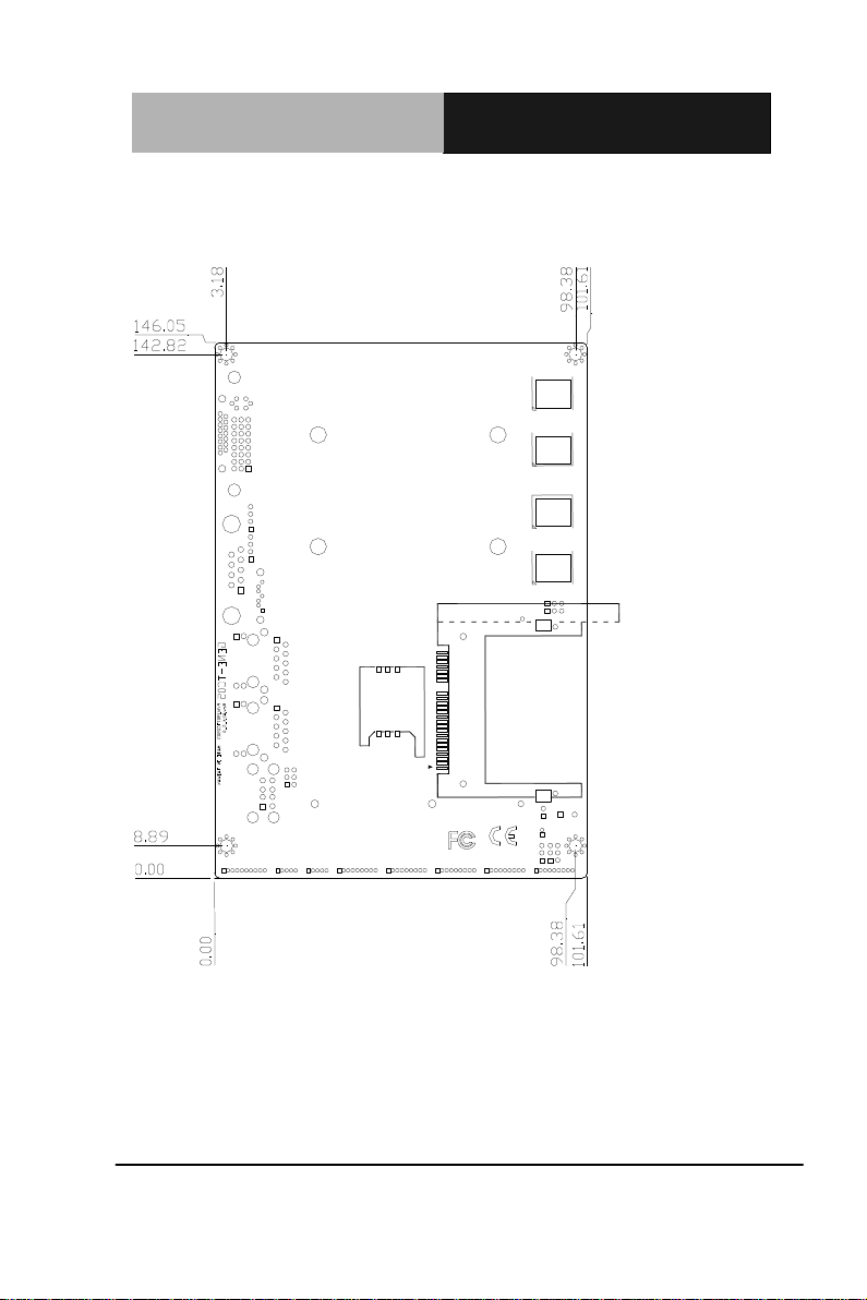
Board Size 5.75" x 4" (146mm x 101.6mm)
Gross Weight 0.4kg
Operating
Temperature
Chapter 1 General Information 1- 4
Supports power supply voltages and
temperature monitoring
and USB interface), LPC
32°F ~ 140°F (0°C ~ 60°C)
WiTAS2: -40°F ~ 185°F (-40°C ~
85°C) (TF-GENE-TC05W2-A10-01)
Page 12

SubCompact Board GENE-TC05
Storage
-40°F ~ 176°F (-40°C ~ 80°C)
Temperature
Operating Humidity 0% ~ 90% relative humidity,
non-condensing
Display: Supports VGA or DVI (Optional) / LVDS LCD
Chip
set Intel
®
E680/E620/E620T
integrated (E620T is for WiTAS2)
Memory Shared system memory up to
512MB
Resolution Up to 1280x1024 for VGA, DVI
Up to 1280x768 for LCD
LCD Interface Up to 24-bit single channel LVDS
I/O
Storage SATA 3.0Gb/s x 1, CFast
Serial Port RS-232 x 5, RS-232/422/485(auto
flow) x 1 (the baud rate of the
serial port should be 9600 during
high temperature operation)
CAN Bus Supports CAN Protocol Version
2.0B, bit rate up to 1M-bit/sec.
USB Port USB2.0 x 4
PS/2 Port Keyboard x 1, Mouse x 1
Touch Screen Support 4/5/8-wire Resistive
Touch Screen
Digital I/O Supports 8-bit (Programmable)
Audio Line-in, Line-out, Mic-in
To turn on the power in ATX mode, please touch the power button
Note:
within 1 second.
Chapter 1 General Information
™ x 1
1 - 5
Page 13

SubCompact Board
G E N E - T C 0 5
Chapter
2
Quick
Installation
Guide
Chapter 2 Quick Installation Guide 2-1
Page 14
SubCompact Board
G E N E - T C 0 5
Always completely disconnect the power cord
from your board whenever you are working on
it. Do not make connections while the power is
on, because a sudden rush of power can
damage sensitive electronic components.
Always ground yourself to remove any static
charge before touching the board. Modern
electronic devices are very sensitive to static
electric charges. Use a grounding wrist strap at
all times. Place all electronic components on a
static-dissipative surface or in a static-shielded
bag when they are not in the chassis
2.1 Safety Precautions
Chapter 2 Quick Installation Guide 2-2
Page 15
SubCompact Board
G E N E - T C 0 5
2.2 Location of Connectors and Jumpers
Component Side
Chapter 2 Quick Installation Guide 2-3
Page 16
SubCompact Board
G E N E - T C 0 5
Solder Side
Chapter 2 Quick Installation Guide 2-4
Page 17
SubCompact Board
G E N E - T C 0 5
2.3 Mechanical Drawing
Component Side
Chapter 2 Quick Installation Guide 2-5
Page 18
SubCompact Board
G E N E - T C 0 5
Solder Side
Chapter 2 Quick Installation Guide 2-6
Page 19

SubCompact Board
G E N E - T C 0 5
Label
Function
JP1
LVDS Operating Voltage Selection
JP2
LVDS Inverter Voltage Selection
JP3
COM2 RI/+5/+12V
JP5
Touch Screen 4/5/8-wire Mode Selection
JP6
Auto Power Button Selection
JP7
RS-232/422/485 Selection-1
JP8
RS-232/422/485 Selection-2
Label
Function
CN1
LVDS Inverter Connector
CN2
LPC Expansion I/F
CN3
Front Panel
CN4
Digital I/O
CN5
COM Port #2
CN6
+5V Output for SATA HDD using
CN7
SYSTEM FAN
CN8
COM Port #3
CN9
+5VSB Output w/ SMBus
CN10
LVDS
2.4 List of Jumpers
The board has a number of jumpers that allow you to configure your
system to suit your application.
The table below shows the function of each of the board's jumpers:
2.5 List of Connectors
The board has a number of connectors that allow you to configure
your system to suit your application. The table below shows the
function of each board's connectors:
Chapter 2 Quick Installation Guide 2-7
Page 20

SubCompact Board
G E N E - T C 0 5
CN11
COM Port #4
CN12
COM Port #5
CN13
COM Port #6
CN14
USB Port #4
CN15
PS/2 Keyboard & Mouse
CN16
Touch Screen I/F
CN17
USB Port #3
CN18
Power Input (Vin)
CN19
RJ-45 Ethernet #1
CN20
RJ-45 Ethernet #2
CN21
SATA
CN22
I2C
CN23
CAN Bus
CN24
USB Port #1 and #2
CN25
Audio Line In/Out and MIC Connector
CN26
CRT/DVI Display
CN27
COM Port #1
CN28
SIM Card Socket
CFD1
CFast™ Disk
PCIE1
Mini Card Slot #1
PCIE2
Mini Card Slot #2
Note:
(1) Because of the limitation of the Intel® processor, the GENE-TC05 needs
battery—CR-2450 with higher capacity to deal with higher power
consumption.
(2)We put the battery-CR-2450 together with the discrete component next
Chapter 2 Quick Installation Guide 2-8
Page 21
SubCompact Board
G E N E - T C 0 5
1
2
3
Open Closed Closed 2-3
to the CPU board to keep the fully energy of the battery, users have to
assemble it yourselves on the “BAT1” connector.
(3)If the CR-2450 battery is in low energy, the RTC (Real Time Clock) will
lose in this condition and users have to change another CR-2450 battery.
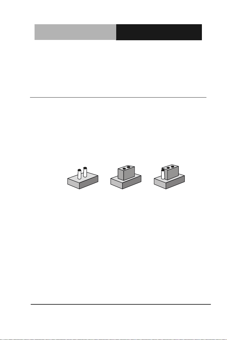
2.6 Setting Jumpers
You configure your card to match the needs of your application by
setting jumpers. A jumper is the simplest kind of electric switch. It
consists of two metal pins and a small metal clip (often protected by a
plastic cover) that slides over the pins to connect them. To “close” a
jumper you connect the pins with the clip.
To “open” a jumper you remove the clip. Sometimes a jumper will
have three pins, labeled 1, 2 and 3. In this case you would connect
either pins 1 and 2 or 2 and 3.
A pair of needle-nose pliers may be helpful when working with
jumpers.
If you have any doubts about the best hardware configuration for your
application, contact your local distributor or sales representative
before you make any change.
Generally, you simply need a standard cable to make most
connections.
Chapter 2 Quick Installation Guide 2-9
Page 22

SubCompact Board
G E N E - T C 0 5
JP1
Function
1-2
+5V
2-3
+3.3V (Default)
JP2
Function
1-2
+12V
2-3
+5V (Default)
JP3
Function
1-2
+12V
3-4
+5V
5-6
RI (Default)
JP5
Function
1-2
4/8-wire (Default)
Open
5-wire
JP6
Function
1-2
Enable (Default)
2-3
Disable
2.7 LVDS Operating Voltage Selection (JP1)
2.8 LVDS Inverter Voltage Selection (JP2)
2.9 COM2 RI/5V/+12V Selection (JP3)
2.10 Touch Screen 4/5/8-wire Mode Selection (JP5)
2.11 Auto Power Button Selection (JP6)
Chapter 2 Quick Installation Guide 2-10
Page 23

SubCompact Board
G E N E - T C 0 5
JP7
Function
1-2
RS-232 (Default)
3-4
RS-422
5-6
RS-485
JP8
Function
1-3, 2-4, 7-9, 8-10
RS-232 (Default)
3-5, 4-6, 9-11, 10-12
RS-422
3-5, 9-11
RS-485
Pin
Signal
1
+5 Volt. / +12 Volt.
2
N/C 3 Ground
4
Ground
5
Backlight Enable (Controlled by CH7308C)
Pin
Signal
1
LAD0
2
LAD1
3
LAD2
4
LAD3
2.12 RS-232/422/485 Selection (JP7)
2.13 RS-232/422/485 Selection (JP8)
2.14 LVDS Inverter Connector (CN1)
Note: The max. rating of pin 1 is 1A
2.15 LPC Expansion I/F (CN2)
Chapter 2 Quick Installation Guide 2-11
Page 24

SubCompact Board
G E N E - T C 0 5
5
+3.3V
6
LFRAME#
7
LRESET#
8
Ground
9
LPC_CLK
10
LDRQ#0
11
LDRQ#1
12
SERIRQ
Pin
Signal
(-) 1-2 (+)
ATX Power-on Button
(-) 3-4 (+)
HDD Active LED
(-) 5-6 (+)
External Speaker
(-) 7-8 (+)
Power LED
(-) 9-10 (+)
System Reset Button
Pin
Signal
Pin
Signal
1
Port 1
2
Port 2
3
Port 3
4
Port 4
5
Port 5
6
Port 6
7
Port 7
8
Port 8
9
+3.3V
10
Ground
BIOS Setting
Connector
Definition
Address
(Register)
F75111 GPIO
Setting
2.16 Front Panel (CN3)
2.17 Digital I/O Connector (CN4)
This connector offers 4-pair of digital I/O functions and address is 6Eh. The
pin definitions are illustrated below:
Note: The max. rating of pin 9 is 1A
Chapter 2 Quick Installation Guide 2-12
Page 25

SubCompact Board
G E N E - T C 0 5
Output
Input
Port 8 @6Eh
Pin 8
21h/Bit7
22h/Bit7
U8 Pin 20 (GPIO 27)
Port 7 @6Eh
Pin 7
21h/Bit6
22h/Bit6
U8 Pin 21 (GPIO 26)
Port 6 @6Eh
Pin 6
21h/Bit5
22h/Bit5
U8 Pin 22 (GPIO 25)
Port 5 @6Eh
Pin 5
21h/Bit4
22h/Bit4
U8 Pin 23 (GPIO 24)
Port 4 @6Eh
Pin 4
21h/Bit3
22h/Bit3
U8 Pin 24 (GPIO 23)
Port 3 @6Eh
Pin 3
21h/Bit2
22h/Bit2
U8 Pin 8 (GPIO 22)
Port 2 @6Eh
Pin 2
21h/Bit1
22h/Bit1
U8 Pin 7 (GPIO 21)
Port 1 @6Eh
Pin 1
21h/Bit0
22h/Bit0
U8 Pin 6 (GPIO 20)
Pin
Signal
Pin
Signal
1
DCDB
2
DSRB
3
RXB
4
RTSB
5
TXB
6
CTSB
7
DTRB
8
RIB / +5V / +12V
9
Ground
Pin
Signal
Pin
Signal
1
TXD-
2
N/C
3
RXD+
4
N/C
5
TXD+
6
N/C
7
RXD-
8
N/C / +5V / +12V
2.18 COM Port #2 (CN5)
Note: The max. rating of pin 8 is 0.5A
RS-232
RS-422
Chapter 2 Quick Installation Guide 2-13
Page 26

SubCompact Board
G E N E - T C 0 5
9
Ground
Pin
Signal
Pin
Signal
1
TXD-
2
N/C
3
N/C 4 N/C 5 TXD+
6
N/C 7 N/C 8 N/C / +5V / +12V
9
Ground
Pin
Signal
1
+5V
2
Ground
Pin
Signal
1
Ground
2
+5 Volt. (Optional) / +12V
3
FAN Sense
Pin
Signal
Pin
Signal
1
DCDC
2
DSRC
3
RXC
4
RTSC
5
TXC
6
CTSC
7
DTRC
8
RIC 9 Ground
RS-485
2.19 +5V Output For SATA HDD (CN6)
Note: The max. output of CN6 is 1A @ 5V
2.20 System Fan (CN7)
2.21 COM Port #3 (CN8)
Chapter 2 Quick Installation Guide 2-14
Page 27

SubCompact Board
G E N E - T C 0 5
Pin
Signal
1
SMBDATA
2
Ground
3
SMBCLK
4
Ground
5
PSON#
6
+5V Standby
Pin
Signal
Pin
Signal
1
Back-Light Enable
2
Back-Light Control
3
LCD Volt.
4
Ground
5
LA_CLK#
6
LA_CLK
7
LCD Volt.
8
Ground
9
LA_DATA#_0
10
LA_DATA_0
11
LA_DATA#_1
12
LA_DATA_1
13
LA_DATA#_2
14
LA_DATA_2
15
LA_DATA#_3
16
LA_DATA_3
17
DDCDATA
18
DDCCLK
19
N/C
20
N/C
21
N/C
22
N/C
23
N/C
24
N/C
25
N/C
26
N/C
27
LCD Volt.
28
Ground
29
N/C
30
N/C
2.22 +5VSB Output w/SMBus (CN9)
2.23 LVDS Output (CN10)
Note: The total max. rating of pin 3, 7, 27 is 3A
Chapter 2 Quick Installation Guide 2-15
Page 28

SubCompact Board
G E N E - T C 0 5
Pin
Signal
Pin
Signal
1
DCDD
2
DSRD
3
RXD
4
RTSD
5
TXD
6
CTSD
7
DTRD
8
RID 9 Ground
Pin
Signal
Pin
Signal
1
DCDE
2
DSRE
3
RXE
4
RTSE
5
TXE
6
CTSE
7
DTRE
8
RIE 9 Ground
Pin
Signal
Pin
Signal
1
DCDF
2
DSRF
3
RXF
4
RTSF
5
TXF 6 CTSF
7
DTRF
8
RIF 9 Ground
Pin
Signal
1
+5V Standby
2
Data4-
2.24 COM Port #4 (CN11)
2.25 COM Port #5 (CN12)
2.26 COM Port #6 (CN13)
2.27 USB Port #4 (CN14)
Chapter 2 Quick Installation Guide 2-16
Page 29

SubCompact Board
G E N E - T C 0 5
3
Data4+
4
Ground
5
Ground
Pin
Signal
Pin
Signal
1
Keyboard Data
2
Keyboard Clock
3
Ground
4
+5V 5 Mouse Data
6
Mouse Clock
Pin
8-wire Signal
5-wire Signal
4-wire Signal
1
Ground
Ground
Ground
2
Top Excite
Top
UL(Y)
3
Bottom Excite
Bottom
UR(H)
4
Left Excite
Left
LL(L)
5
Right Excite
Right
LR(X)
6
Top Sense
N/C
SENSE
7
Bottom Sense
N/C
N/C 8 Left Sense
N/C
N/C 9 Right Sense
N/C
N/C
Pin
Signal
1
+5V Standby
2
Data3-
3
Data3+
4
Ground
2.28 PS/2 Keyboard and Mouse (CN15)
2.29 Touch Screen I/F (CN16)
2.30 USB Port #3 (CN17)
Chapter 2 Quick Installation Guide 2-17
Page 30

SubCompact Board
G E N E - T C 0 5
5
Ground
Pin
Signal
1
+12V
2
Ground
Pin
Signal
Pin
Signal
R1
GPHY_MDIO0+
R2
GPHY_MDIO0-
R3
GPHY_MDIO1+
R4
GPHY_MDIO1-
R5
TCD0
R6
TCD1
R7
GPHY_MDIO2+
R8
GPHY_MDIO2-
R9
GPHY_MDIO3+
R10
GPHY_MDIO3-
L1
SPD100_LED
L2
SPD1K_LED
L3
ACT_LED
L4
+3.3V
Pin
Signal
Pin
Signal
R1
MDIO0+
R2
MDIO0-
R3
MDIO1+
R4
MDIO1-
R5
TCD0
R6
TCD1
R7
MDIO2+
R8
MDIO2-
R9
MDIO3+
R10
MDIO3-
L1
SPD100_LED
L2
SPD1K_LED
L3
ACT_LED
L4
+3.3V
2.31 Power Input (Vin) (CN18)
2.32 RJ-45 Ethernet #1 (CN19)
2.33 RJ-45 Ethernet #2 (CN20)
Chapter 2 Quick Installation Guide 2-18
Page 31

SubCompact Board
G E N E - T C 0 5
Pin
Signal
1
Ground
2
TX+ 3 TX- 4 Ground
5
RX- 6 RX+
7
Ground
Pin
Signal
1
+3.3V
2
SCL
3
SDA
4
Ground
Pin
Signal
1
CANH
2
Ground
3
CANL
4
N/C
Pin
Signal
Pin
Signal
1
+5V Standby
5
+5V Standby
2.34 SATA Connector (CN21)
2.35 I2C (CN22)
2.36 CAN Bus (CN23)
2.37 USB Port #1 & #2 (CN24)
Chapter 2 Quick Installation Guide 2-19
Page 32

SubCompact Board
G E N E - T C 0 5
2
Data1-
6
Data2-
3
Data1+
7
Data2+
4
Ground
8
Ground
Pin
Signal
1
MIC_L
2
MIC_R
3
Ground
4
Line IN_L
5
Line IN_R
6
Ground
7
Line OUT_L
8
Ground
9
Line OUT_R
10
+5V
Pin
Signal
Pin
Signal
C1
RED
C2
GREEN
C3
BLUE
C4
HSYNC
C5
Ground
C6
N/C 1 DVI_TDC2#
2
DVI_TDC2
3
Ground
4
DDCCLK
5
DDCDATA
6
DVI_CLK
7
DVI_DATA
8
VSYNC
9
DVI_TDC1#
10
DVI_TDC1
11
Ground
12
N/C
2.38 Audio Line In/Out and MIC Connector (CN25)
2.39 DVI/CRT Display (CN26)
DVI
Chapter 2 Quick Installation Guide 2-20
Page 33

SubCompact Board
G E N E - T C 0 5
13
N/C
14
+5V
15
Ground
16
DVI_DET
17
DVI_TDC0#
18
DVI_TDC0
19
Ground
20
N/C
21
N/C
22
Ground
23
DVI_TLC
24
DVI_TLC#
25
Ground
26
Ground
27
N/C
28
N/C
Pin
Signal
Pin
Signal
29
DDCCLK
30
N/C
31
+5V
32
HSYNC
33
GREEN
34
Ground
35
N/C
36
Ground
37
Ground
38
VSYNC
39
BLUE
40
Ground
41
DDCDATA
42
RED
43
CRT_PLUG#
Pin
Signal
Pin
Signal
1
DCDA
2
RXA
3
TXA
4
DTRA
5
Ground
6
DSRA
7
RTSA
8
CTSA
9
RIA
CRT
2.40 COM Port #1 (CN27)
Chapter 2 Quick Installation Guide 2-21
Page 34

SubCompact Board
G E N E - T C 0 5
Pin
Signal
Pin
Signal
1
UIM_PWR
2
UIM_RST
3
UIM_CLK
4
Ground
5
UIM_VPP
6
UIM_DATA
Pin
Signal
S1
Ground
S2
SATA_TX+
S3
SATA_TX-
S4
Ground
S5
SATA_RX-
S6
SATA_RX+
S7
Ground
P1
N/C
P2
Ground
P3
N/C
P4
N/C
P5
N/C
P6
N/C
P7
Ground
P8
CFD_LED#
P9
N/C
P10
N/C
P11
N/C
P12
N/C
2.41 SIM Card Socket (CN28)
2.42 CFast™ Disk (CFD1)
Chapter 2 Quick Installation Guide 2-22
Page 35

SubCompact Board
G E N E - T C 0 5
P13
+3.3V
P14
+3.3V
P15
Ground
P16
Ground
P17
N/C
Pin
Signal
Pin
Signal
1
PCIE_WAKE#
2
+3.3V Standby
3
N/C 4 Ground
5
N/C 6 +1.5V
7
N/C 8 UIM_PWR
9
Ground
10
UIM_DATA
11
MCARD_CLK1#
12
UIM_CLK
13
MCARD_CLK1
14
UIM_RESET
15
Ground
16
UIM_VPP
17
N/C
18
Ground
19
N/C
20
W_DISABLE#1
21
Ground
22
PCIE_RST#
23
PCIE_RXN1
24
+3.3V Standby
25
PCIE_RXP1
26
Ground
27
Ground
28
+1.5V
29
Ground
30
SMBCLK
31
PCIE_TXN1
32
SMBDATA
33
PCIE_TXP1
34
Ground
35
Ground
36
USB_Data5-
37
Ground
38
USB_Data5+
39
+3.3V Standby
40
Ground
2.43 Mini Card Slot #1 (PCIE1)
Chapter 2 Quick Installation Guide 2-23
Page 36

SubCompact Board
G E N E - T C 0 5
41
+3.3V Standby
42
N/C
43
Ground
44
N/C
45
N/C
46
N/C
47
N/C
48
+1.5V
49
N/C
50
Ground
51
N/C
52
+3.3V Standby
Pin
Signal
Pin
Signal
1
PCIE_WAKE#
2
+3.3V Standby
3
N/C 4 Ground
5
N/C 6 +1.5V
7
N/C 8 N/C 9 Ground
10
N/C
11
MCARD_CLK2#
12
N/C
13
MCARD_CLK2
14
N/C
15
Ground
16
N/C
17
N/C
18
Ground
19
N/C
20
W_DISABLE#2
21
Ground
22
PCIE_RST#
23
PCIE_RXN2
24
+3.3V Standby
25
PCIE_RXP2
26
Ground
27
Ground
28
+1.5V
29
Ground
30
SMBCLK
31
PCIE_TXN2
32
SMBDATA
33
PCIE_TXP2
34
Ground
35
Ground
36
N/C
37
Ground
38
N/C
2.44 Mini Card Slot #2 (PCIE2)
Chapter 2 Quick Installation Guide 2-24
Page 37

SubCompact Board
G E N E - T C 0 5
39
+3.3V Standby
40
Ground
41
+3.3V Standby
42
N/C
43
Ground
44
N/C
45
N/C
46
N/C
47
N/C
48
+1.5V
49
N/C
50
Ground
51
N/C
52
+3.3V Standby
Chapter 2 Quick Installation Guide 2-25
Page 38

SubCompact Board
G E N E - T C 0 5
部件名稱
有毒有害物質或元素
鉛
(Pb)
汞
(Hg) 鎘 (Cd)
六價鉻
(Cr(VI))
多溴聯苯
(PBB)
多溴二苯醚
(PBDE)
印刷電路板
及其電子元件
× ○ ○ ○ ○
○
外部信號
連接器及線材
× ○ ○ ○ ○
○
O:表示該有毒有害物質在該部件所有均質材料中的含量均在
SJ/T 11363-2006標準規定的限量要求以下。
X:表示該有毒有害物質至少在該部件的某一均質材料中的含量超出
SJ/T 11363-2006標準規定的限量要求。
備註:此產品所標示之環保使用期限,系指在一般正常使用狀況下。
Below Table for China RoHS Requirements
產品中有毒有害物質或元素名稱及含量
AAEON Main Board/ Daughter Board/ Backplane
Chapter 2 Quick Installation Guide 2-26
Page 39

SubCompact Board GENE-TC05
Chapter
3
AMI
BIOS Setup
Chapter 3 AMI BIOS Setup 3-1
Page 40

SubCompact Board GENE-TC05
3.1 System Test and Initialization
These routines test and initialize board hardware. If the routines
encounter an error during the tests, you will either hear a few short
beeps or see an error message on the screen. There are two kinds
of errors: fatal and non-fatal. The system can usually continue the
boot up sequence with non-fatal errors.
The GENE-TC05 CMOS memory has an integral lithium battery
backup for system time retention. However, you will need to replace
the complete unit when it finally runs down.
Chapter 3 AMI BIOS Setup 3-2
Page 41

SubCompact Board GENE-TC05
3.2 AMI BIOS Setup
AMI BIOS ROM has a built-in Setup program that allows users to
modify the basic system configuration. This type of information is
stored in NVRAM so that it retains the Setup information when the
power is turned off.
Entering Setup
Power on the computer and press <Del > or <F2> immediately. This
will allow you to enter Setup.
Main
Set the date, use tab to switch between date elements.
Advanced
Enable disable boot option for legacy network devices.
Chipset
host bridge parameters.
Boot
Enables/disable quiet boot option.
Security
Set setup administrator password.
Save&Exit
Exit system setup after saving the changes.
Chapter 3 AMI BIOS Setup 3-3
Page 42

SubCompact Board GENE-TC05
Setup Menu
‘Delete’ Key to enter Setup menu
Press
Main
Chapter 3 AMI BIOS Setup 3-4
Page 43

SubCompact Board GENE-TC05
Advanced
Chapter 3 AMI BIOS Setup 3-5
Page 44

SubCompact Board GENE-TC05
ACPI Settings
Options summary:
Enable Hibernation
Disable
Enable Optimal Default,
Failsafe Default
Enables or Disables System ability to Hibernate (OS/S4 Sleep S t ate). This
option may be not effective with some OS.
ACPI Sleep State
Suspend Disabled
S1 (CPU Stop Clock)
S3 (Suspend to RAM) Optimal Default,
Failsafe Default
Chapter 3 AMI BIOS Setup 3-6
Page 45

SubCompact Board GENE-TC05
Select the highest ACPI sleep state the
SUSPEND button is pressed.
CPU Configuration
system will enter when the
Options summary:
Intel SpeedStep
Disabled
Enabled Optimal Default,
Enable or Disable Intel(R) SpeedStep(tm)
Hyper-Threading
Disabled
Failsafe Default
Chapter 3 AMI BIOS Setup 3-7
Page 46

SubCompact Board GENE-TC05
Enabled Optimal Default,
Failsafe Defa
ult
Enabled for Windows XP and Linux (OS optimized for Hyper-Threading
Technology) and Disabled for other OS (OS not optimized for
Hyper-Threading Technology)
Execute Disable Bit
Disabled
Enabled Optimal Default,
Failsafe Default
XD can prevent certain classes of malicious buffer overflow attacks when
combined with a supporting OS (Windows Server 2003 SP1, Wind ows XP
SP2, SuSE Linux 9.2, RedHat Enterprise 3 Update 3.)
Limit CPUID Maximum
Disabled Optimal Default,
Failsafe Default
Enabled
Disabled for Windows XP
Intel Virtualization Technology
Disabled Optimal Default,
Failsafe Default
Enabled
When enabled, a VMM can utilize the additional hardware capabilities
provided by Vanderpo ol Technology
C-States
Disabled
Enabled Optimal Default,
Failsafe Default
Enable or Disable C2 and above
Chapter 3 AMI BIOS Setup 3-8
Page 47

SubCompact Board GENE-TC05
Enhanced C1
Disabled Optimal Default,
Enabled
Enable or Disable Enhanced C1 State
Enhanced C2
Disable
Enable Optimal Default,
Enable or Disable Enhanced C2 State
Enhanced C3
Disable Optimal Default,
Enable
Enable or Disable Enhanced C3 State
Enhanced C4
Disable
Enable Optimal Default,
Enable or Disable Enhanced C4 State
Failsafe Defa
ult
Failsafe Default
Failsafe Default
Failsafe Default
Chapter 3 AMI BIOS Setup 3-9
Page 48

SubCompact Board GENE-TC05
Digital IO
Options summary:
GPI0-3 Device
Set GPI0 as Input or Output
GPO0-3 Device
Set GPO0-3 as Input or Output
Chapter 3 AMI BIOS Setup 3-10
Input Optimal Default,
Failsafe Default
Output
Input
Output Optimal Default,
Failsafe Default
Page 49

SubCompact Board GENE-TC05
AHCI SATA Configuration
Options summary:
PORT 0
Disabled
Enable Optimal Default,
Failsafe Default
Enable/Disable PORT 0 Set transfer mode programming
PORT 1
Disabled
Enable Optimal Default,
Failsafe Default
Enable/Disable PORT 1 Set transfer mode programming
Chapter 3 AMI BIOS Setup 3-11
Page 50

SubCompact Board GENE-TC05
Wake On Lan Configuration
Options summary:
Wake On Lan
Enable/Disable WOL
Chapter 3 AMI BIOS Setup 3-12
Disabled
Enable Optimal Default,
Failsafe Default
Page 51

SubCompact Board GENE-TC05
USB Configuration
Options summary:
Legacy USB Support
Enabled Optimal Default,
Failsafe Default
Disabled
Auto
Enables BIOS Support for Legacy USB Support. When enabled, USB
can be functional in legacy environment like DOS.
AUTO option disables legacy support if no USB devices are connected
USB transfer time-out
1 sec
5 sec
Chapter 3 AMI BIOS Setup 3-13
Page 52

SubCompact Board GENE-TC05
10 sec
20 sec Optimal Default,
Failsafe Default
The time-out value for Control, Bulk, and Interrupt transfers
Device reset time-out
1 sec
5 sec
10 sec
20 sec Optimal Default,
Failsafe Default
USB mass storage device Start Unit command time-out
Device Name (Emulation
Type)
Auto Optimal Default,
Failsafe Default
Floppy
Forced FDD
Hard Disk
CDROM
If Auto. USB devices less than 530MB will be emulated as Floppy and
remaining as Floppy and remaining as hard drive. Forced FDD option
can be used to force a HDD formatted drive to boot as FDD(Ex. ZIP
drive)
Chapter 3 AMI BIOS Setup 3-14
Page 53

SubCompact Board GENE-TC05
Second Super IO Configuration
Chapter 3 AMI BIOS Setup 3-15
Page 54

SubCompact Board GENE-TC05
Serial Port 3 Configuration
Chapter 3 AMI BIOS Setup 3-16
Page 55

SubCompact Board GENE-TC05
Serial Port 4 Configuration
Chapter 3 AMI BIOS Setup 3-17
Page 56

SubCompact Board GENE-TC05
Serial Port 5 Configuration
Chapter 3 AMI BIOS Setup 3-18
Page 57

SubCompact Board GENE-TC05
Serial Port 6 Configuration
Options summary:
Serial Port
Disabled
Enabled Optimal Default,
Enable or Disable Serial Port (COM)
Change Settings
IO=3E8h; IRQ=10; Optimal Default,
(Serial Port 3)
IO=3E8h;
IRQ=3,4,5,6,7,9,10,11,12;
Failsafe Default
Failsafe Default
Chapter 3 AMI BIOS Setup 3-19
Page 58

SubCompact Board GENE-TC05
IO=2E8h;
Change Settings
(Serial Port 4)
Change Settings
IRQ=3,4,5,6,7,9,10,1
IO=2F0h;
1,12;
IRQ=3,4,5,6,7,9,10,11,12;
IO=2E0h;
IRQ=3,4,5,6,7,9,10,11,12;
IO=2E8h; IRQ=11; Optimal Default,
Failsafe Default
IO=3E8h;
IRQ=3,4,5,6,7,9,10,11,12;
IO=2E8h;
IRQ=3,4,5,6,7,9,10,11,12;
IO=2F0h;
IRQ=3,4,5,6,7,9,10,11,12;
IO=2E0h;
IRQ=3,4,5,6,7,9,10,11,12;
IO=2F0h; IRQ=7; Optimal Default,
(Serial Port 5)
Chapter 3 AMI BIOS Setup 3-20
IO=3E8h;
IRQ=3,4,5,6,7,9,10,11,12;
IO=2E8h;
IRQ=3,4,5,6,7,9,10,11,12;
IO=2F0h;
IRQ=3,4,5,6,7,9,10,11,12;
Failsafe Default
Page 59

SubCompact Board GENE-TC05
IO=2E0h;
IRQ=3,4,5,6,7,9,10,1
Change Settings
IO=2E0h; IRQ=5; Optimal Default,
(Serial Port 6)
IO=3E8h;
IRQ=3,4,5,6,7,9,10,11,12;
IO=2E8h;
IRQ=3,4,5,6,7,9,10,11,12;
IO=2F0h;
IRQ=3,4,5,6,7,9,10,11,12;
IO=2E0h;
IRQ=3,4,5,6,7,9,10,11,12;
Select an optimal setting for Super IO device
1,12;
Failsafe Default
Chapter 3 AMI BIOS Setup 3-21
Page 60

SubCompact Board GENE-TC05
Super IO Configuration
Chapter 3 AMI BIOS Setup 3-22
Page 61

SubCompact Board GENE-TC05
Serial Port 1 Configuration
Chapter 3 AMI BIOS Setup 3-23
Page 62

SubCompact Board GENE-TC05
Serial Port 2 Configuration
Options summary:
Serial Port
Disabled
Enabled Optimal
Enable or Disable Serial Port (COM)
Change Settings
(Serial Port 1)
IO=3F8h; IRQ=4;
IO=3E8h;
IRQ=3,4,5,6,7,9,10,11,12;
Chapter 3 AMI BIOS Setup 3-24
Default,
Failsafe
Default
Page 63

SubCompact Board GENE-TC05
IO=2E8h;
IRQ=3,4,5,6,7,9,10,1
IO=2F0h;
IRQ=3,4,5,6,7,9,10,11,12;
IO=2E0h;
IRQ=3,4,5,6,7,9,10,11,12;
Change Settings
(Serial Port 2)
IO=2F8h; IRQ=3;
IO=3E8h;
IRQ=3,4,5,6,7,9,10,11,12;
IO=2E8h;
IRQ=3,4,5,6,7,9,10,11,12;
IO=2F0h;
IRQ=3,4,5,6,7,9,10,11,12;
IO=2E0h;
IRQ=3,4,5,6,7,9,10,11,12;
Select an optimal setting for Super IO device
Serial Port 2 Device
RS232 Optimal
1,12;
Type
RS422
RS485
Select RS232, RS422 or RS485
Default,
Failsafe
Default
Chapter 3 AMI BIOS Setup 3-25
Page 64

SubCompact Board GENE-TC05
H/W Monitor
Chapter 3 AMI BIOS Setup 3-26
Page 65

SubCompact Board GENE-TC05
Chipset
Chapter 3 AMI BIOS Setup 3-27
Page 66

SubCompact Board GENE-TC05
North Bridge Chipset Configuration
Options summary:
IGD Mode Select
Chapter 3 AMI BIOS Setup 3-28
Enabled, 1MB
Enabled, 4MB
Enabled, 8MB Optimal Default, Failsafe
Default
Enabled, 16MB
Enabled, 32MB
Enabled, 48MB
Enabled, 64MB
Page 67

SubCompact Board GENE-TC05
Select the amount of system memory used by the Inte
Device.
grated Graphics
MSAC Mode Select
Enabled, 512MB
Enabled, 256MB Optimal Default, Failsafe
Default
Enabled, 128MB
Select the size of the graphics memory aperture and untrusted space.
Used by the Integrated Graphics Device
LVDS Backlight
Controller
100%
90%
80%
70%
60%
50% Optimal Default, Failsafe
Default
40%
30%
20%
10%
0%
Adjust backlight brightness
Chapter 3 AMI BIOS Setup 3-29
Page 68

SubCompact Board GENE-TC05
Boot Display Configuration
Options summary:
Primary Display
Auto Optimal Default,
Failsafe Default
IGD
PEG
Select which graphics controller to use as the primary boot display
Boot Display Device
Integrated L V DS
External DVI
External CRT Optimal Default,
Failsafe Default
Chapter 3 AMI BIOS Setup 3-30
Page 69

SubCompact Board GENE-TC05
Select Boot Display Device
Flat Panel Scaling
Select Flat Panel Scaling
Flat Panel Type
Select Flat Panel Type
DPST Control
Auto Optimal Default,
Failsafe Default
Forced
Disabled
640x480 18Bit
640x480 24Bit
800x600 18Bit
800x600 24Bit
1024x768 18Bit Optimal Default,
Failsafe Default
1024x768 24Bit
1280x768 18Bit
1280x768 24Bit
VBIOS-Default
DPST Disabled
DPST Enabled L1
DPST Enabled L2
DPST Enabled L3 Optimal Default,
Failsafe Default
DPST Enabled L4
DPST Enabled L5
Chapter 3 AMI BIOS Setup 3-31
Page 70

SubCompact Board GENE-TC05
Select DPST Control
South Bridge Chipset Configuration
Options summary:
Primary Display
Auto Optimal Default,
Failsafe Default
IGD
PEG
Select which graphics controller to use as the primary boot display
Chapter 3 AMI BIOS Setup 3-32
Page 71

SubCompact Board GENE-TC05
PCI Express Ports Configuration
Chapter 3 AMI BIOS Setup 3-33
Page 72

SubCompact Board GENE-TC05
PCI Express Root Port 0
Chapter 3 AMI BIOS Setup 3-34
Page 73

SubCompact Board GENE-TC05
PCI Express Root Port 1
Chapter 3 AMI BIOS Setup 3-35
Page 74

SubCompact Board GENE-TC05
PCI Express Root Port 2
Chapter 3 AMI BIOS Setup 3-36
Page 75

SubCompact Board GENE-TC05
PCI Express Root Port 3
Chapter 3 AMI BIOS Setup 3-37
Page 76

SubCompact Board GENE-TC05
PCI-to-PCI Bridge
Options summary:
PCI Express Root Port 0
Disabled
Enabled Optimal Default,
PCI Express Root Port 0 Settings
PCI Express Root Port 1
Disabled
Enabled Optimal Default,
PCI Express Root Port 1 Settings
PCI Express Root Port 2
Chapter 3 AMI BIOS Setup 3-38
Disabled
Failsafe Default
Failsafe Default
Page 77

SubCompact Board GENE-TC05
Enabled Optimal Default,
Failsafe Defa
PCI Express Root Port 2 Settings
PCI Express Root Port 3
Disabled
Enabled Optimal Default,
Failsafe Default
PCI Express Root Port 3 Settings
Extra Bus Reserved
0 Optimal Default,
Failsafe Default
Extra Bus Reserved (0-7) for bridges behind this Root Bridge
ult
Chapter 3 AMI BIOS Setup 3-39
Page 78

SubCompact Board GENE-TC05
PPM Config
Options summary:
C-state POPUP
Disabled
Enabled Optimal Default,
Enable/Disable C-state POPUP
Chapter 3 AMI BIOS Setup 3-40
Failsafe Default
Page 79

SubCompact Board GENE-TC05
Boot
Options summary:
Quiet Boot
Disabled
Enabled Optimal Default,
Failsafe Default
Enables or disables Quiet Boot option
Fast Boot
Disabled
Enabled Optimal Default,
Failsafe Default
Enables/Disables boot with initialization of a minimal set of devices
required to launch active boot option. Has no effect for BBS boot options
Chapter 3 AMI BIOS Setup 3-41
Page 80

SubCompact Board GENE-TC05
T
Setup Prompt Timeout
Integer
Number of seconds to wait for setup activation key. 65535(0xFFFF)
means indefinite waiting.
Bootup NumLock State
On
Off Optimal Default,
Failsafe Default
Select the keyboard NumLock state
GateA20 Active
Upon Request Default
Always
UPON REQUEST - GA20 can be disabled using BIOS services.
ALWAYS - do not allow disabling GA20; this option is useful when any R
code is executed above 1MB.
Option ROM Messages
Force BIOS Default
Keep Current
Set display mode for Option ROM
Interrupt 19 Capture
Disabled
Enabled Default
Enabled: Allows Option ROMs to trap Int 19
Chapter 3 AMI BIOS Setup 3-42
Page 81

SubCompact Board GENE-TC05
Security
Cha
nge User/Supervisor Password
You can install a Supervisor password, and if you install a
supervisor password, you can then install a user password. A user
password does not provide access to many of the features in the
Setup utility. If you highlight these items and press Enter, a dialog
box appears which lets you enter a password. You can enter no
more than six letters or numbers. Press Enter after you have
typed in the password. A second dialog box asks you to retype the
password for confirmation. Press Enter after you have retyped it
correctly. The password is required at boot time, or when the user
enters the Setup utility.
Removing the Password
Highlight this item and type in the current password. At the next
dialog box press Enter to disable password protection.
Chapter 3 AMI BIOS Setup 3-43
Page 82

SubCompact Board GENE-TC05
Chapter 3 AMI BIOS Setup 3-44
Page 83

SubCompact Board GENE-TC05
Save & Exit
Chapter 3 AMI BIOS Setup 3-45
Page 84

SubCompact Board GENE-TC05
Chapter
4
Driver
Inst
Chapter 4 Driver Installation 4 -1
allation
Page 85

SubCompact Board GENE-TC05
.
The GENE-TC05 comes with a CD-ROM that contains all drivers
your need.
Follow the sequence below to install the drivers:
Step 1 – Install Chipset Driver
Step 2 – Install VGA Driver
Step 3 – Install PCH EG20T Driver
Step 4 – Install LAN Driver
Step 5 – Install Audio Driver
Step 6 – Install Touch Driver
Please read following instructions for detailed installations.
Chapter 4 Driver Installation 4 -2
Page 86

SubCompact Board GENE-TC05
4.1 Installation:
Insert the GENE-TC05 DVD-ROM into the CD-ROM Drive. And
install the drivers from Step 1 to Step 6 in order.
Step 1 – Install Chipset Driver
1. Click on the Step 1 - Chipset INF folder and double click
on the Setup.exe file
2. Follow the instructions that the window shows
3. The system will help you to install the driver automatically
Step 2 – Install VGA Driver
For the VGA drivers, there are three types. 2a is for CRT only, 2b is
for DVI only, and 2c is for LVDS and CRT only.
1. Click on the Step 2a - Graphic CRT only folder and
double click on WindowsDriverSETUP file
Click on the Step 2b - Graphic DVI only folder and double
click on WindowsDriverSETUP file
Click on the Step 2c- Graphic LVDS and CRT folder and
double click on WindowsDriverSETUP file
2. Follow the instructions that the window shows
3. The system will help you to install the driver automatically
Step 3 – Install PCH EG20T Driver
1. Click on the Step 3 - PCH EG20T folde r and sele ct the
OS your system is
2. Double click on .exe file located in each OS folder
3. Follow the instructions that the window shows
The system will help you to install the driver automatically
4.
Chapter 4 Driver Installation 4 -3
Page 87

SubCompact Board GENE-TC05
Step 4 – Install LAN Driver
1. Click on the Step 4 - Intel 82574L Ethernet folder and
select the OS your system is
2. Double click on .exe file located in each OS folder
3. Follow the instructions that the window shows
4. The system will help you to install the driv er automatically
Step 5 – Install Audio Driver
1. Click on the Step 5 - Realtek ALC888 Audio Codec
folder and select the OS your system is
2. Double click on .exe file located in each OS folder
3. Follow the instructions that the window shows
4. The system will help you to install the driv er automatically
Step 6 – Install Touch Driver
1. Click on the Step 6 - PenMount Touch 6000 series
(Option) folder and select the OS your system is
2. Double click on the Setup.exe file located in each OS
folder
3. Follow the instructions that the window shows you
4. The system will help you install the driver automatically
Chapter 4 Driver Installation 4 -4
Page 88

SubCompact Board GENE-TC05
A
Programming the
W
atchdog Timer
Appendix
Appendix A Programming the Watchdog Timer A-1
Page 89

SubCompact Board GENE-TC05
A.1 Programming
GENE-TC05 utilizes W83627DHG-P chipset as its watchdog timer
controller.
Below are the procedures to complete its configuration and the
AAEON intial watchdog timer program is also attached based on
which you can develop customized program to fit your application.
Configuring Sequence Description
There are th
Unlock W83627DHG
Select register of
watchdog timer
Enable the function of
the watchdog timer
Use the function of the
watchdog timer
Lock W83627DHG
ree steps to complete the configuration setup:
(1) Enter the W83627DHG config Mode
(2) Modify the data of configuration registers
Appendix A Programming the Watchdog Timer A-2
Page 90

SubCompact Board GENE-TC05
(3) Exit the W83627DHG config Mode. Undesired result may
occur if the config Mode is not exited normally.
(1) Enter the W83627DHG config Mode
To enter the W83627DHG config Mode, two special I/O write
operations are to be performed during Wait for Key state. To
ensure the initial state of the key-check logic, it is necessary to
perform two write operations to the Special Address port (2EH).
The different enter keys are provided to select configuration ports
(2Eh/2Fh) of the next step.
Address Port Data Port
87h,87h: 2Eh 2Fh
(2) Modify the Data of the Registers
All configuration registers can be accessed after entering the config
Mode. Before accessing a selected register, the content of Index
07h must be changed to the LDN to which the register belongs,
except some Global registers.
(3) Exit the W83627DHG config Mode
The exit key is provided to select configuration ports (2Eh/2Fh) of
the next step.
Address Port Data Port
0aah: 2Eh 2Fh
WatchDog Timer Register I (Index=F5h, Default=00h)
CRF5 (PLED and KBC P20 Control Mode Register)
Bit 7-5 : select PLED mode
= 000 Power LED pin is driven high.
= 001 Power LED pin outputs 0.5Hz pulse
with 50% duty cycle.
Appendix A Programming the Watchdog Timer A-3
Page 91

SubCompact Board GENE-TC05
= 010 Power LED pin is driven low.
= 011 Power LED pin outputs 2Hz pulse
with 50% duty cycle.
= 100 Power LED pin outputs 1Hz pulse
with 50% duty cycle.
= 101 Power LED pin outputs 4Hz pulse
with 50% duty cycle.
= 110 Power LED pin outputs 0.25Hz pulse
with 50% duty cycle.
=111 Power LED pin outputs 0.25Hz pulse
with 50% duty cycle..
Bit 4 : WDTO# count mode is 1000 times faster.
= 0 Disable.
= 1 Enable.
Bit 3 : select WDTO# count mode.
= 0 second
= 1 minute
Bit 2 : Enable the rising edge of keyboard Reset
(P20) to force Time-out event.
= 0 Disable
= 1 Enable
Bit 1 : Disable / Enable the WDTO# output low
pulse to the KBRST# pin (PIN60)
= 0 Disable
= 1 Enable
Bit 0 : Reserved.
Appendix A Programming the Watchdog Timer A-4
Page 92

SubCompact Board GENE-TC05
WatchDog Timer Register II (Index=F6h, Default=00h)
Bit 7-0 = 0 x 00 Time-out Disable
= 0 x 01 Time-out occurs after 1
second/minute
= 0 x 02 Time-out occurs after 2
second/minutes
= 0 x 03 Time-out occurs after 3
second/minutes
………………………………..
= 0 x FF Time-out occurs after 255
second/minutes
WatchDog Timer Register III (Index=F7h, Default=00h)
Bit 7 : Mouse interrupt reset Enable or Disable
= 1 Watchdog Timer is reset upon a
Mouse interrupt
= 0 Watchdog Timer is not affected by
Mouse interrupt
Bit 6 : Keyboard interrupt reset Enable or
Disable
= 1 Watchdog Timer is reset upon a
Keyboard interrupt
= 0 Watchdog Timer is not affected by
Keyboard interrupt
Bit 5 : Force Watchdog Timer Time-out. Write
Only
Appendix A Programming the Watchdog Timer A-5
Page 93

SubCompact Board GENE-TC05
= 1 Force Watchdog Timer time-out
event: this bit is self-clearing
Bit 4 : Watchdog Timer Status. R/W
= 1 Watchdog Timer time-out occurred
= 0 Watchdog Timer counting
Bit 3-0 : These bits select IRQ resource for
Watchdog. Setting of 2 selects SMI.
Appendix A Programming the Watchdog Timer A-6
Page 94

SubCompact Board GENE-TC05
A.2 W83627DHG Watchdog Timer Initial Program
Example: Setting 10 sec. as Watchdog timeout interval
;///////////////////////////////////////////////////////////////////////////////////////////////
Mov dx,2eh ;Enter W83627DHG config mode
Mov al,87h (out 87h to 2eh twice)
Out dx,al
Out dx,al
;///////////////////////////////////////////////////////////////////////////////////////////////
Mov al,07h
Out dx,al
Inc dx
Mov al,08h ;Select Logical Device 8 (GPIO Port
2)
Out dx,al
;///////////////////////////////////////////////////////////////////////////////////////////////
Dec dx
Mov al,30h ;CR30 (GP20 ~GP2 7)
Out dx,al
Inc dx
Mov al,01h ;Activate GPIO2
Out dx,al
Appendix A Programming the Watchdog Timer A-7
Page 95

SubCompact Board GENE-TC05
;///////////////////////////////////////////////////////////////////////////////////////////////
Dec dx
Mov al,0f5h ;CRF5 (PLED mode register)
Out dx,al
Inc dx
In al,dx
And al,not 08h ;Set second as counting unit
Out dx,al
;///////////////////////////////////////////////////////////////////////////////////////////////
Dec dx
Mov al,0f6h ; CRF6
Out dx,al
Inc dx
Mov al,10 ;Set timeout interval as 10 sec.
Out dx,al
;///////////////////////////////////////////////////////////////////////////////////////////////
Dec dx ;Exit W83627DHG config mode
Mov al,0aah (out 0aah to 2eh once)
Out dx,al
;///////////////////////////////////////////////////////////////////////////////////////////////
Appendix A Programming the Watchdog Timer A-8
Page 96

SubCompact Board GENE-TC05
Appendix
I/O Information
B
Appendix B I/O Information B - 1
Page 97

SubCompact Board GENE-TC05
B.1 I/O Address Map
Appendix B I/O Information B - 2
Page 98

SubCompact Board GENE-TC05
Appendix B I/O Information B - 3
Page 99

SubCompact Board GENE-TC05
B.2 Memory Address Map
Appendix B I/O Information B - 4
Page 100

SubCompact Board GENE-TC05
B.3 IRQ Mapping Chart
Appendix B I/O Information B - 5
 Loading...